
This document is a general product description and is subject to change without notice. Hynix Electronics does not assume any responsibility
for use of circuits described. No patent licenses are implied.
Rev 04 / Apr. 2001 Hynix Semiconductor
HY62CT08081E
Series
32Kx8bit CMOS SRAM
Document Title
32K x8 bit 5.0V Low Power Slow SRAM
Revision History
Revision No History Draft Date Remark
00 Initial Nov.01.2000 Preliminary
01 Marking Information Add Dec.05.2000 Preliminary
Revised
-
DC / AC Characteristics
-
AC Test Condition Add : 5pF Test Load
02 Revised Feb.13.2001 Final
-
Remove L-Part
-
Change LL-Part Isb1 Limit @E.T/I.T
: 15uA => 20uA
03 Revised Feb.21.2001 Final
-
Marking Information Change : SOP Type
04 Changed Logo Apr.30.2001 Final
-
HYUNDAI -> hynix
-
Marking Information Change
HY62CT08081E Series
Rev 04 / Apr. 2001
2
DESCRIPTION
The HY62CT08081E is a high-speed, low power
and 32,786 X 8-bits CMOS Static Random
Access Memory fabricated using Hynix's high
performance CMOS process technology. It is
suitable for use in low voltage operation and
battery back-up application. This device has a
data retention mode that guarantees data to
remain valid at the minimum power supply
voltage of 2.0 volt.
FEATURES
∑
Fully static operation and Tri-state output
∑
TTL compatible inputs and outputs
∑
Low power consumption
∑
Battery backup
- 2.0V(min.) data retention
∑
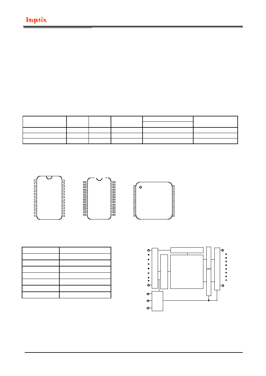
Standard pin configuration
- 28 pin 600mil PDIP
- 28 pin 330mil SOP
- 28 pin 8x13.4 mm TSOP-I
(Standard)
Product
Voltage
Speed
Operation
Standby Current(uA)
Temperature
No.
(V)
(ns)
Current(mA)
LL
(
∞
C)
HY62CT08081E-C
5.0
55/70/85
10
10
0~70(Normal)
HY62CT08081E-E
5.0
55/70/85
10
20
-25~85(Extended)
HY62CT08081E-I
5.0
55/70/85
10
20
-40~85(Industrial)
Note 1. Current value is max.
PIN CONNECTION
1
2
3
4
5
6
7
8
9
10
11
12
13
14
28
27
26
25
24
23
22
21
20
19
18
17
16
15
Vcc
/WE
A8
A9
A11
/OE
A10
/CS
I/O8
I/O7
I/O6
I/O5
I/O4
A14
A12
A7
A6
A5
A4
A3
A2
A1
A0
I/O1
I/O2
I/O3
Vss
A13
1
2
3
4
5
6
7
8
9
10
11
12
13
14
28
27
26
25
24
23
22
21
20
19
18
17
16
15
Vcc
/WE
A8
A9
A11
/OE
A10
/CS
I/O8
I/O7
I/O6
I/O5
I/O4
A14
A12
A7
A6
A5
A4
A3
A2
A1
A0
I/O1
I/O2
I/O3
Vss
A13
1
2
3
4
5
6
7
8
9
10
11
12
13
14
28
27
26
25
24
23
22
21
20
19
18
17
16
15
A10
/CS
I/O7
I/O6
I/O5
I/O4
Vss
I/O3
I/O2
I/O1
A0
A1
A2
/OE
A11
A9
A8
A13
/WE
Vcc
A14
A12
A7
A6
A5
A4
A3
I/O8
PDIP SOP TSOP-I(Standard)
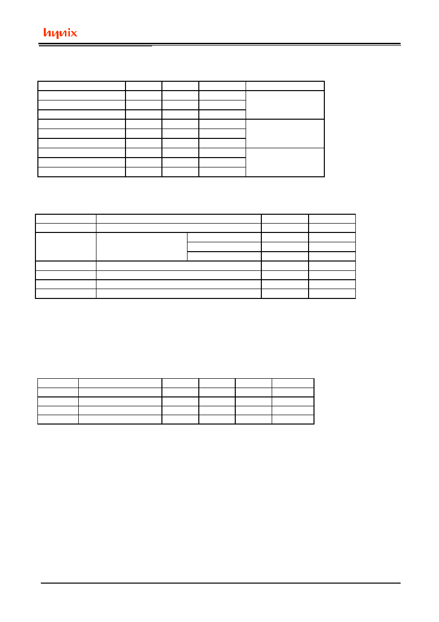
PIN DESCRIPTION BLOCK DIAGRAM
Pin Name
Pin Function
/CS
Chip Select
/WE
Write Enable
/OE
Output Enable
A0 ~ A14
Address Inputs
I/O1 ~ I/O8
Data Input/Output
Vcc
Power(
+
5.0V)
Vss
Ground
A14
COLUMN DECODER
A0
ROW DECODER
MEMORY ARRAY
512x512
SENSE AMP
OUTPUT BUFFER
I/O1
I/O8
ADD INPUT BUFFER
/CS
/OE
/WE
WRITE DRIVER
CONTROL
LOGIC
HY62CT08081E Series
Rev 04 / Apr. 2001
2
ORDERING INFORMATION
Part No.
Speed
Power
Temp
Package
HY62CT08081E-DPC
55/70/85 LL-part
0 to 70
∞
C
HY62CT08081E-DPE
55/70/85 LL-part -25 to 85
∞
C
HY62CT08081E-DPI
55/70/85 LL-part -40 to 85
∞
C
PDIP
HY62CT08081E-DGC
55/70/85 LL-part
0 to 70
∞
C
HY62CT08081E-DGE
55/70/85 LL-part -25 to 85
∞
C
HY62CT08081E-DGI
55/70/85 LL-part -40 to 85
∞
C
SOP
HY62CT08081E-DTC
55/70/85 LL-part
0 to 70
∞
C
HY62CT08081E-DTE
55/70/85 LL-part -25 to 85
∞
C
HY62CT08081E-DTI
55/70/85 LL-part -40 to 85
∞
C
TSOP-I Standard
ABSOLUTE MAXIMUM RATING (1)
Symbol
Parameter
Rating
Unit
Vcc, V
IN,
V
OUT
Power Supply, Input/Output Voltage
-0.3 to 7.0
V
HY62CT08081E-C 0 to 70
∞
C
HY62CT08081E-E
-25 to 85
∞
C
T
A
Operating Temperature
HY62CT08081E-I
-40 to 85
∞
C
T
STG
Storage Temperature
-65 to 150
∞
C
P
D
Power Dissipation
1.0
W
I
OUT
Data Output Current
50
mA
T
SOLDER
Lead Soldering Temperature & Time
260
∑
10
∞
C
∑
sec
Note
1. Stresses greater than those listed under ABSOLUTE MAXIMUM RATINGS may cause permanent
damage to the device. This is stress rating only and the functional operation of the device under these or
any other conditions above those indicated in the operation of this specification is not implied.
Exposure to the absolute maximum rating conditions for extended period may affect reliability.
RECOMMENDED DC OPERATING CONDITIONS
Symbol
Parameter
Min.
Typ.
Max.
Unit
Vcc
Power Supply Voltage
4.5
5.0
5.5
V
Vss
Ground
0
0
0
V
V
IH
Input High Voltage
2.2
-
Vcc+0.3
V
V
IL
Input Low Voltage
-0.3
(1)
-
0.8
V
Note
1. V
IL
= -3.0V for pulse width less than 50ns
HY62CT08081E Series
Rev 04 / Apr. 2001
3
TRUTH TABLE
/CS /WE /OE
Mode
I/O Operation
H
X
X Standby
High-Z
L
H
H Output Disabled High-Z
L
H
L Read
Data Out
L
L
X Write
Data In
Note
1. H=V
IH
, L=V
IL
, X=Don't Care
DC CHARACTERISTICS
Vcc = 5V
±
10%, T
A
= 0
∞
C to 70
∞
C (Normal) / -25
∞
C to 85
∞
C (Extended) / -40
∞
C to 85
∞
C (Industrial),
unless otherwise specified.
Symbol
Parameter
Test Condition
Min. Typ. Max. Unit
I
LI
Input Leakage Current
Vss < V
IN
< Vcc
-1
-
1
uA
I
LO
Output Leakage Current
Vss < V
OUT
< Vcc, /CS = V
IH
or
/
OE
=
V
IH
or /WE = V
IL
-1
-
1
uA
Icc
Operating Power Supply
Current
/CS = V
IL
,
V
IN
= V
IH
or V
IL,
I
I/O =
0mA
-
-
10
mA
I
CC1
Average Operating Current /CS = V
IL,
V
IN
= V
IH
or V
IL,
Min. Duty Cycle = 100%, I
I/O =
0mA
-
-
50
mA
I
SB
TTL Standby Current
(TTL Inputs)
/CS= V
IH,
V
IN
= V
IH
or V
IL
-
-
1
mA
I
SB1
CMOS Standby Current
/CS > Vcc - 0.2V,
(CMOS Inputs)
V
IN
> Vcc - 0.2V or
0~70
∞
C
-
-
10
uA
V
IN
< Vss + 0.2V
-25~85
∞
C or
-40~85
∞
C
-
-
20
uA
V
OL
Output Low Voltage
I
OL
= 2.1mA
-
-
0.4
V
V
OH
Output High Voltage
I
OH =
-1.0mA
2.4
-
-
V
Note : Typical values are at Vcc =5.0V, T
A
= 25
∞
C

HY62CT08081E Series
Rev 04 / Apr. 2001
4
AC CHARACTERISTICS
Vcc = 5V
±
10%, T
A
= 0
∞
C to 70
∞
C (Normal) / -25
∞
C to 85
∞
C (Extended) / -40
∞
C to 85
∞
C (Industrial)
unless otherwise specified.
-55
-70
-85
Min. Max. Min. Max. Min
Max.
1 tRC
Read Cycle Time
55
-
70
-
85
-
ns
2 tAA
Address Access Time
-
55
-
70
-
85
ns
3 tACS
Chip Select Access Time
-
55
-
70
-
85
ns
4 tOE
Output Enable to Output Valid
-
25
-
35
-
45
ns
5 tCLZ
Chip Select to Output in Low Z
10
-
10
-
10
-
ns
6 tOLZ
Output Enable to Output in Low Z
5
-
5
-
5
-
ns
7 tCHZ
Chip Disable to Output in High Z
0
20
0
30
0
30
ns
8 tOHZ
Out Disable to Output in High Z
0
20
0
30
0
30
ns
9 tOH
Output Hold from Address Change
5
-
5
-
5
-
ns
10 tWC
Write Cycle Time
55
-
70
-
85
-
ns
11 tCW
Chip Selection to End of Write
45
-
60
-
75
-
ns
12 tAW
Address Valid to End of Write
45
-
60
-
75
-
ns
13 tAS
Address Set-up Time
0
-
0
-
0
-
ns
14 tWP
Write Pulse Width
40
-
50
-
60
-
ns
15 tWR
Write Recovery Time
0
-
0
-
0
-
ns
16 tWHZ Write to Output in High Z
0
20
0
25
0
30
ns
17 tDW
Data to Write Time Overlap
25
-
30
-
40
-
ns
18 tDH
Data Hold from Write Time
0
-
0
-
0
-
ns
19 tOW
Output Active from End of Write
5
-
5
-
5
-
ns
AC TEST CONDITIONS
T
A
= 0
∞
C to 70
∞
C (Normal) / -25
∞
C to 85
∞
C (Extended) / -40
∞
C to 85
∞
C (Industrial)
unless otherwise specified.
Parameter
Value
Input Pulse Level
0.8V to 2.4V
Input Rise and Fall Time
5ns
Input and Output Timing Reference Level
1.5V
Output Load
tCLZ,tOLZ,tCHZ,tOHZ,tWHZ,tOW
CL = 5pF + 1TTL Load
Others
CL = 100pF + 1TTL Load
READ CYCLE
WRITE CYCLE
Symbol
Parameter
#
Unit