
This document is a general product description and is subject to change without notice. Hynix Semiconductor does not assume any
responsibility for use of circuits described. No patent licenses are implied.
Rev.07 / Aug. 2001 Hynix Semiconductor
HY62UF16201A Series
128Kx16bit full CMOS SRAM
Document Title
128K x16 bit 3.0V Super Low Power Full CMOS Slow SRAM
Revision History
Revision No History Draft Date Remark
05 Divide output load into two factors Dec.10. 2000 Final
- tCLZ,tOLZ,tBLZ,tCHZ,tOHZ,tBHZ,tWHZ,tOW
- Others
Add the marking information
06 Correct the PKG dimension(E1) Aug. 01. 2001
Add the dimension and the marking information of the 6x8 PKG size
07 Separate the part number(HY62UF16201AF1) for the 6x8 PKG Aug. 31. 2001
size from the 7x8 PKG size(HY62UF16201AF)
HY62UF16201A Series
Rev.07 / Aug. 2001
2
DESCRIPTION
The HY62UF16201A is a high speed, super low
power and 2Mbit full CMOS SRAM organized as
131,072 words by 16bits. The HY62UF16201A
uses high performance full CMOS process
technology and is designed for high speed and
low power circuit technology. It is particularly well-
suited for the high density low power system
application. This device has a data retention
mode that guarantees data to remain valid at a
minimum power supply voltage of 1.2V.
FEATURES
∑
Fully static operation and Tri-state output
∑
TTL compatible inputs and outputs
∑
Battery backup(LL/SL-part)
-. 1.2V(min) data retention
∑
Standard pin configuration
-. 48-FBGA
Product
Voltage
Speed
Operation
Standby Current(uA)
Temperature
No.
(V)
(ns)
Current/Icc(mA)
LL
SL
(
∞
C)
HY62UF16201A
2.7~3.3 55/70/85/100
3
10
2
0~70
HY62UF16201A-I
2.7~3.3 55/70/85/100
3
10
2
-40~85(I)
Notes :
1. Blank : Commercial, I : Industrial
2. Current value is max.
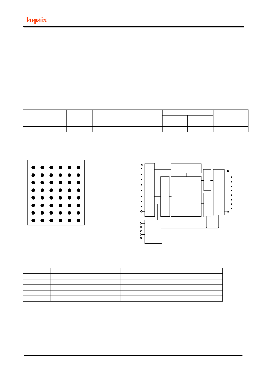
PIN CONNECTION BLOCK DIAGRAM
/LB
IO9
IO10
/OE A0
A1
A2
NC
/UB A3
A4
/CS IO1
IO11 A5
A6
IO2
IO3
Vss IO12 NC
A7
IO4
Vcc
Vcc IO13 NC
A16 IO5
Vss
IO15 IO14 A14 A15 IO6
IO7
IO16 NC
A12 A13 /WE IO8
NC
A8
A9
A10 A11 NC
48-FBGA(Top View)
PIN DESCRIPTION
Pin Name
Pin Function
Pin Name
Pin Function
/CS
Chip Select
I/O1~I/O16
Data Inputs / Outputs
/WE
Write Enable
A0~A16
Address Inputs
/OE
Output Enable
Vcc
Power(2.7V~3.3V)
/LB
Lower Byte Control(I/O1~I/O8)
Vss
Ground
/UB
Upper Byte Control(I/O9~I/O16) NC
No Connection
MEMORY ARRAY
128K x 16
ROW
DECODER
SENSE AMP
WRITE DRIVER
DATA I/O
BUFF
ER
I/O1
I/O16
COLUMNDECODER
CONTROL
LOGIC
ADD INPUT BUFFER
A0
A16
/CS
/OE
/LB
/UB
/WE
HY62UF16201A Series
Rev.07 / Aug. 2001
2
ORDERING INFORMATION
Part No.
Speed
Power Temp.
Package
HY62UF16201ALLF
55/70/85/100 LL-part
FBGA(7mm X 8mm)
HY62UF16201ALLF-I
55/70/85/100 LL-part
I
FBGA(7mm X 8mm)
HY62UF16201ASLF
55/70/85/100 SL-part
FBGA(7mm X 8mm)
HY62UF16201ASLF-I
55/70/85/100 SL-part
I
FBGA(7mm X 8mm)
HY62UF16201ALLF1
55/70/85/100 LL-part
FBGA(6mm X 8mm)
HY62UF16201ALLF1-I
55/70/85/100 LL-part
I
FBGA(6mm X 8mm)
HY62UF16201ASLF1
55/70/85/100 SL-part
FBGA(6mm X 8mm)
HY62UF16201ASLF1-I
55/70/85/100 SL-part
I
FBGA(6mm X 8mm)
Note :
1. Blank : Commercial, I : Industrial
ABSOLUTE MAXIMUM RATINGS (1)
Symbol
Parameter
Rating
Unit
Remark
V
IN,
V
OUT
Input/Output Voltage
-0.2 to 3.6
V
Vcc
Power Supply
-0.2 to 4.6
V
T
A
Operating Temperature
0 to 70
∞
C
HY62UF16201A
-40 to 85
∞
C
HY62UF16201A-I
T
STG
Storage Temperature
-55 to 150
∞
C
P
D
Power Dissipation
1.0
W
T
SOLDER
Ball Soldering Temperature & Time
260
∑
10
∞
C
∑
sec
Note
1. Stresses greater than those listed under ABSOLUTE MAXIMUM RATINGS may cause permanent
damage to the device. This is stress rating only and the functional operation of the device under these or
any other conditions above those indicated in the operation of this specification is not implied.
Exposure to the absolute maximum rating conditions for extended period may affect reliability.
TRUTH TABLE
I/O
/CS /WE /OE /LB /UB
Mode
I/O1~I/O8 I/O9~I/O16
Power
H
X
X
X
X Deselected
High-Z
High-Z
Standby
X
X
X
H
H Deselected
High-Z
High-Z
Standby
L
H
H
L
X Output Disabled
High-Z
High-Z
Active
L
H
H
X
L Output Disabled
High-Z
High-Z
Active
L
H
L
L
H Read
D
OUT
High-Z
Active
H
L
High-Z
D
OUT
L
L
D
OUT
D
OUT
L
L
X
L
H Write
D
IN
High-Z
Active
H
L
High-Z
D
IN
L
L
D
IN
D
IN
Note :
1. H=V
IH
, L=V
IL
, X=don't care
2. UB, LB(Upper, Lower Byte enable)
These active LOW inputs allow individual bytes to be written or read.
When LB is LOW, data is written or read to the lower byte, I/O 1 -I/O 8.
When UB is LOW, data is written or read to the upper byte, I/O 9 -I/O 16.

HY62UF16201A Series
Rev.07 / Aug. 2001
3
RECOMMENDED DC OPERATING CONDITION
Symbol
Parameter
Min.
Typ.
Max.
Unit
Vcc
Supply Voltage
2.7
3.0
3.3
V
Vss
Ground
0
0
0
V
V
IH
Input High Voltage
2.2
-
Vcc+0.3
V
V
IL
Input Low Voltage
-0.3
(1)
-
0.6
V
Note :
1. VIL = -1.5V for pulse width less than 30ns
DC ELECTRICAL CHARACTERISTICS
T
A
= 0
∞
C to 70
∞
C/ -40
∞
C to 85
∞
C (I)
Symbol
Parameter
Test Condition
Min. Typ. Max. Unit
I
LI
Input Leakage Current
Vss < V
IN
< Vcc
-1
-
1
uA
I
LO
Output Leakage Current Vss < V
OUT
< Vcc, /CS = V
IH
or
/
OE
=
V
IH
or /WE = V
IL,
/
UB
=
/LB = V
IH
-1
-
1
uA
Icc
Operating Power Supply
Current
/CS = V
IL
, V
IN
= V
IH
or V
IL,
I
I/O =
0mA
-
-
3
mA
Cycle Time=Min.100% duty,
/CS = V
IL,
V
IN
= V
IH
or V
IL,
I
I/O =
0mA
-
-
45
mA
I
CC1
Average Operating
Current
Cycle time = 1us,
/CS < 0.2V,
V
IN
<0.2V, I
I/O =
0mA
5
mA
I
SB
Standby
Current
(TTL Input)
/CS = V
IH
or
/UB & /LB = V
IH,
V
IN
= V
IH
or V
IL
-
-
0.3
mA
SL
-
-
2
uA
I
SB1
Standby Current
(CMOS Input)
/CS > Vcc - 0.2V or
/UB = /LB > Vcc - 0.2V,
V
IN
> Vcc - 0.2V or
LL
-
0.5
10
uA
V
IN
< Vss + 0.2V
V
OL
Output Low Voltage
I
OL
= 2.1mA
-
-
0.4
V
V
OH
Output High Voltage
I
OH =
-1.0mA
2.4
-
-
V
Notes :
1. Typical values are at Vcc = 3.0V, T
A
= 25
∞
C
2. Typical values are sampled and not 100% tested
CAPACITANCE
(Temp = 25
∞
C, f= 1.0MHz)
Symbol
Parameter
Condition Max. Unit
C
IN
Input Capacitance(Add, /CS, /WE, /OE) V
IN
= 0V
8
pF
C
OUT
Output Capacitance(I/O)
V
I/O
= 0V
10
pF
Note :
1. These parameters are sampled and not 100% tested
HY62UF16201A Series
Rev.07 / Aug. 2001
4
AC CHARACTERISTICS
T
A
=0
∞
C to 70
∞
C/ -40
∞
C to 85
∞
C (I),unless otherwise specified
-55
-70
-85
-10
Min Max Min Max Min Max Min Max
READ CYCLE
1 tRC
Read Cycle Time
55
-
70
-
85
-
100
-
ns
2 tAA
Address Access Time
-
55
-
70
-
85
-
100 ns
3 tACS
Chip Select Access Time
-
55
-
70
-
85
-
100 ns
4 tOE
Output Enable to Output Valid
-
30
-
35
-
40
-
50 ns
5 tBA
/LB, /UB Access Time
-
55
-
70
-
85
-
100 ns
6 tCLZ
Chip Select to Output in Low Z
10
-
10
-
10
-
20
-
ns
7 tOLZ
Output Enable to Output in Low Z
5
-
5
-
5
-
5
-
ns
8 tBLZ
/LB, /UB Enable to Output in Low Z
5
-
5
-
5
-
5
-
ns
9 tCHZ
Chip Deselection to Output in High Z
0
30
0
30
0
30
0
30 ns
10 tOHZ
Out Disable to Output in High Z
0
30
0
30
0
30
0
30 ns
11 tBHZ
/LB, /UB Disable to Output in High Z
0
30
0
30
0
30
0
30 ns
12 tOH
Output Hold from Address Change
10
-
10
-
10
-
15
-
ns
WRITE CYCLE
13 tWC
Write Cycle Time
55
-
70
-
85
-
100
-
ns
14 tCW
Chip Selection to End of Write
50
-
60
-
70
-
80
-
ns
15 tAW
Address Valid to End of Write
50
-
60
-
70
-
80
-
ns
16 tBW
/LB, /UB Valid to End of Write
50
-
60
-
70
-
80
-
ns
17 tAS
Address Set-up Time
0
-
0
-
0
-
0
-
ns
18 tWP
Write Pulse Width
45
-
50
-
55
-
75
-
ns
19 tWR
Write Recovery Time
0
-
0
-
0
-
0
-
ns
20 tWHZ Write to Output in High Z
0
20
0
25
0
30
0
35 ns
21 tDW
Data to Write Time Overlap
25
-
30
-
35
-
45
-
ns
22 tDH
Data Hold from Write Time
0
-
0
-
0
-
0
-
ns
23 tOW
Output Active from End of Write
5
-
5
-
5
-
10
-
ns
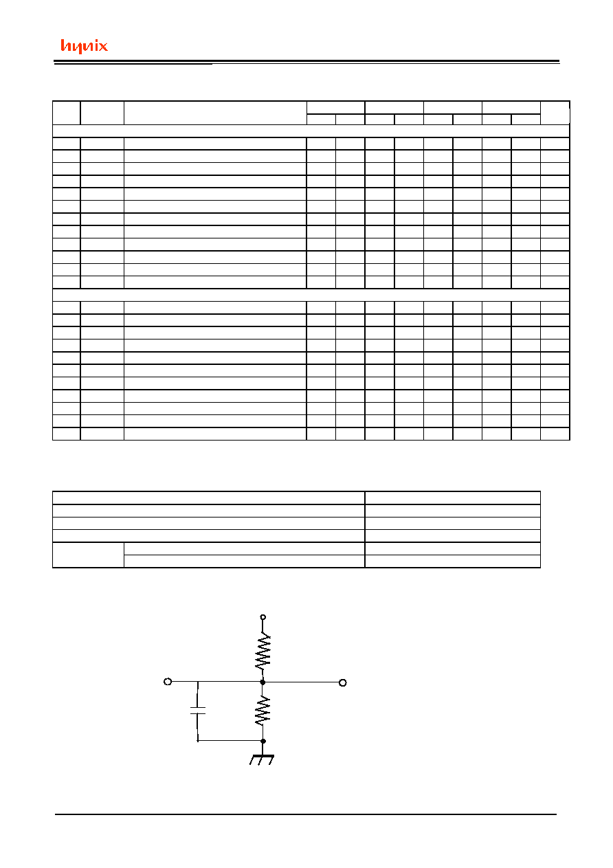
AC TEST CONDITIONS
T
A
= 0
∞
C to 70
∞
C/ -40
∞
C to 85
∞
C (I),unless otherwise specified
Parameter
Value
Input Pulse Level
0.4V to 2.2V
Input Rise and Fall Time
5ns
Input and Output Timing Reference Level
1.5V
tCLZ,tOLZ,tBLZ,tCHZ,tOHZ,tBHZ,tWHZ,tOW
CL = 5pF + 1TTL Load
Output Load
Others
CL = 30pF + 1TTL Load
AC TEST LOADS
D
OUT
1728 Ohm
CL(1)
1029 Ohm
V
TM
= 2.8V
Note :
1. Including jig and scope capacitance
Parameter
Unit
Symbol
#

HY62UF16201A Series
Rev.07 / Aug. 2001
5
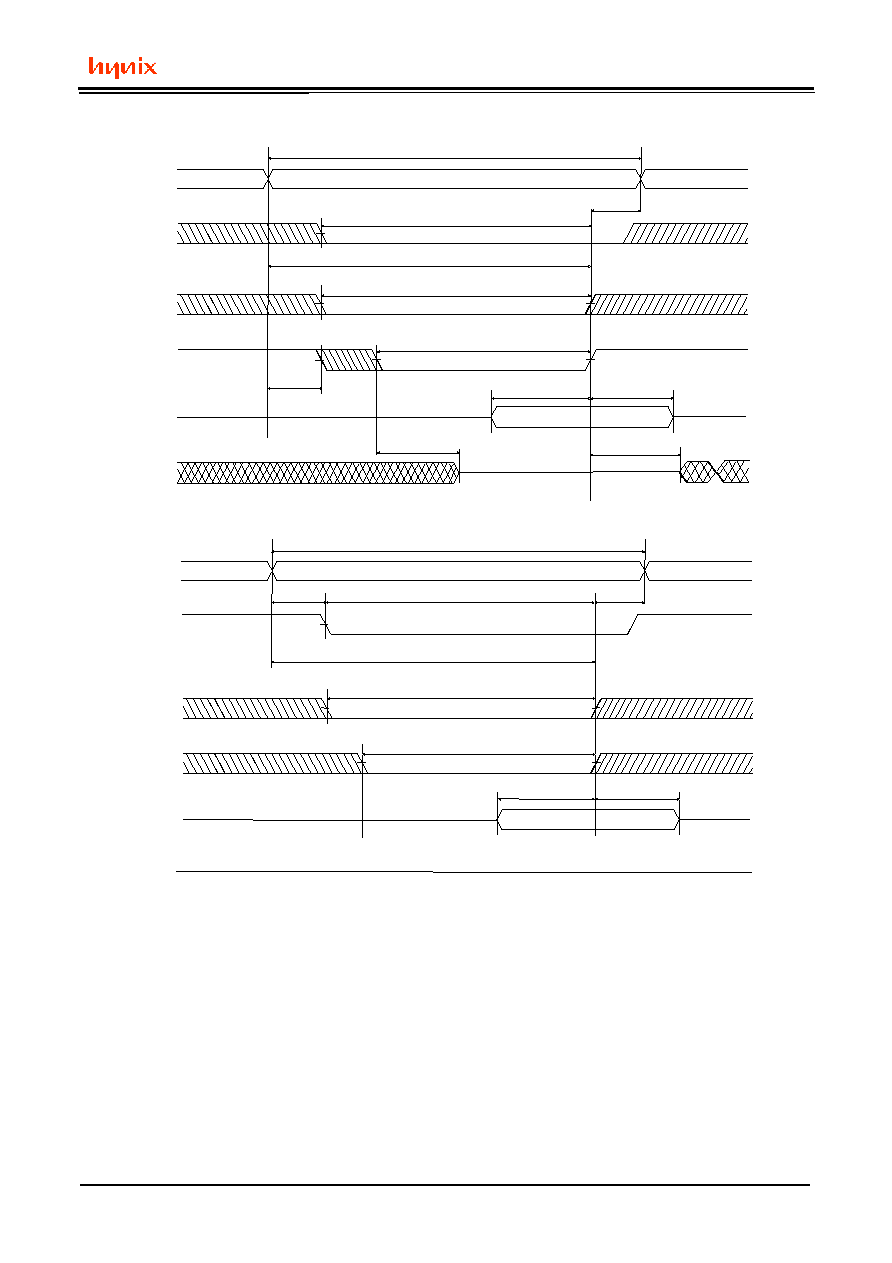
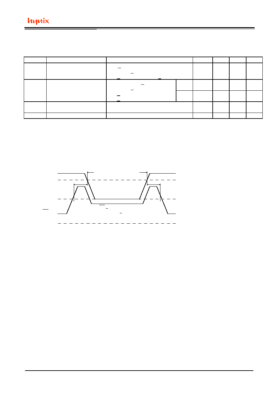
TIMING DIAGRAM
READ CYCLE 1(Note 1,4)
READ CYCLE 2(Note 2,3,4)
ADDR
Data
Out
tRC
tAA
Data Valid
Previous Data
tOH
tOH
READ CYCLE 3(Note 1,2,4)
/CS
/UB, /LB
Data
Out
tACS
Data Valid
tCLZ(3)
tCHZ(3)
Notes:
A read occurs during the overlap of a low /OE, a high /WE, a low /CS1 and low /UB and/or /LB.
2. /OE = V
IL
3. Transition is measured + 200mV from steady state voltage.
This parameter is sampled and not 100% tested.
4. /CS in high for the standby, low for active
/UB and /LB in high for the standby, low for active
ADDR
tRC
/CS
tAA
tACS
tOH
Data Valid
High-Z
Data
Out
/UB ,/ LB
/OE
tBA
tOE
tCLZ
(3)
tBLZ
(3)
tOLZ
(3)
tCHZ
(3)
tBHZ
(3)
tOHZ
(3)
HY62UF16201A Series
Rev.07 / Aug. 2001
6
WRITE CYCLE 1 (1,4,8) (/WE Controlled)
WRITE CYCLE 2 (1,4,8) (/CS Controlled)
Notes:
1. A write occurs during the overlap of a low /WE, a low /CS1 and low /UB and/or /LB.
2. tWR is measured from the earlier of /CS, /LB, /UB, or /WE going high to the end of write cycle.
3. During this period, I/O pins are in the output state so that the input signals of opposite phase to the
output must not be applied.
4. If the /CS, /LB and /UB low transition occur simultaneously with the /WE low transition or after the
/WE transition, outputs remain in a high impedance state.
5. Q(data out) is the same phase with the write data of this write cycle.
6. Q(data out) is the read data of the next address.
7. Transition is measured +200mV from steady state.
This parameter is sampled and not 100% tested.
8. /CS in high for the standby, low for active
/UB and /LB in high for the standby, low for active
Data Valid
ADDR
Data
Out
/
CS
/
UB
,
/
LB
/
WE
tWC
tCW
tWR
(2)
tBW
tAW
tWP
Data In
High-Z
tAS
tWHZ
(3,7)
tDW
tDH
tOW
(5)
(6)
Data Valid
ADDR
Data
Out
/
CS
/
UB
,
/
LB
/
WE
tWC
tCW
tWR
(2)
tBW
tAW
tWP
Data In
tDW
tDH
High-Z
High-Z
tAS
HY62UF16201A Series
Rev.07 / Aug. 2001
7
DATA RETENTION ELECTRIC CHARACTERISTIC
T
A
=0
∞
C to 70
∞
C/ -40
∞
C to 85
∞
C (I),unless otherwise specified
Symbol
Parameter
Test Condition
Min.
Typ. Max. Unit
V
DR
Vcc for Data Retention
/CS > Vcc - 0.2V or
/UB = /LB > Vcc-0.2V,
1.2
-
3.3
V
V
IN
> Vcc - 0.2V or V
IN
< Vss + 0.2V
I
CCDR
Data Retention Current
Vcc=1.5V, /CS > Vcc - 0.2V or
/UB = /LB > Vcc-0.2V,
LL
-
-
10
uA
V
IN
> Vcc - 0.2V or
SL
-
-
2
uA
V
IN
< Vss + 0.2V
tCDR
Chip Deselect to Data
Retention Time
See Data Retention Timing Diagram
0
-
-
ns
tR
Operating Recovery Time
tRC
(3)
-
-
ns
Notes:
1. Typical values are under the condition of T
A
= 25
∞
C.
2. Typical Values are sampled and not 100% tested
3. tRC is read cycle time.
DATA RETENTION TIMING DIAGRAM
CS
VDR
CS > VCC-0.2V
tCDR
tR
VSS
VCC
2.7V
DATA RETENTION MODE
or /UB &/LB
or /UB = /LB > Vcc ≠ 0.2V
HY62UF16201A Series
Rev.07 / Aug. 2001
8
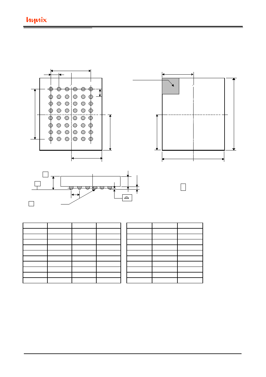
PACKAGE INFORMATION
48ball Fine Pitch Ball Grid Array Package(F)
BOTTOM VIEW
TOP VIEW
B
A
A1 CORNER
B1/2
INDEX AREA
6
5
4
3
2
1
A
A
B
C
D
C
C1
E
F
G
C1/2
C1/2
H
B1/2
B1
SIDE VIEW
5
E1
E2
C
E
SEATING PLANE
4
A
r
3 D(DIAMETER)
[ HY62UF16201AF ] [ HY62UF16201AF1 ]
Symbol
Min.
Typ.
Max.
Min.
Typ.
Max.
A
-
0.75
-
-
0.75
-
B
-
3.75
-
-
3.75
-
B1
6.90
7.00
7.10
5.90
6.00
6.10
C
-
5.25
-
-
5.25
-
C1
7.90
8.00
8.10
7.90
8.00
8.10
D
0.3
0.35
0.4
0.3
0.35
0.4
E
-
-
1.10
-
1.0
1.10
E1
0.75
0.80
0.85
-
0.75
-
E2
0.17
-
-
0.2
0.25
0.3
r
-
-
0.12
-
-
0.08
Note
1. DIMENSIONING AND TOLERANCING PER ASME Y14. 5M-1994.
2. ALL DIMENSIONS ARE MILLIMETERS.
3. DIMENSION "D" IS MEASURED AT THE MAXIMUM SOLDER
BALL DIAMETER IN A PLANE PARALLEL TO DATUM C.
4. PRIMARY DATUM C(SEATING PLANE) IS DEFINED BY THE
CROWN OF THE SOLDER BALLS.
5. THIS IS A CONTROLLING DIMENSION.
HY62UF16201A Series
Rev.07 / Aug. 2001
9
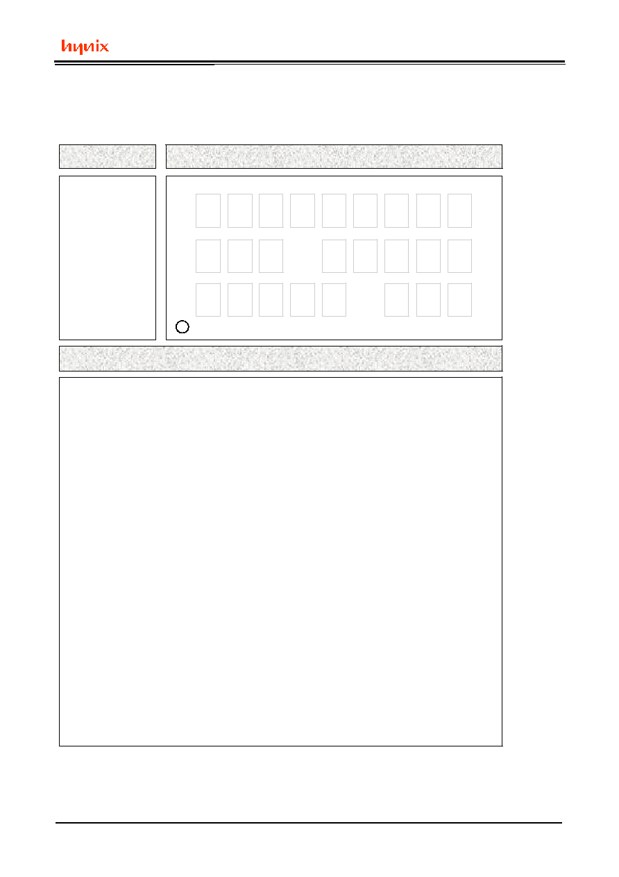
MARKING INSTRUCTION
[ HY62UF16201AF ]
Package
Marking Example
H
Y
U
F
6
2
1
A
c
s
s
t
y
y
w
w
p
x
x
x
x
x
K
O
R
FBGA
(7mm x 8mm)
Index
∑ HYUF621Ac
: Part Name
c
: Power Consumption
- L
: Low Low Power
- S
: Super Low Power
∑ ss
: Speed
- 55
: 55ns
- 70
: 70ns
- 85
: 85ns
- 10
: 100ns
∑ t
: Temperature
- C
: Industrial ( -0 ~ 70
∞
C )
- I
: Industrial ( -40 ~ 85
∞
C )
∑ yy
: Year (ex : 00 = year 2000, 01= year 2001)
∑ ww
: Work Week ( ex : 12 = work week 12 )
∑ p
: Process Code
:
A(7.0mm X 8.0mm)
∑ xxxxx
: Lot No.
∑ KOR
: Origin Country
Note
- Capital Letter
: Fixed Item
- Small Letter
: Non-fixed Item

HY62UF16201A Series
Rev.07 / Aug. 2001
10
[ HY62UF16201AF1 ]
Package
Marking Example
H
Y
U
F
6
2
1
A
c
s
s
t
y
y
w
w
p
x
x
x
x
x
K
O
R
FBGA
(6mm x 8mm)
Index
∑ HYUF621Ac
: Part Name
c
: Power Consumption
- L
: Low Low Power
- S
: Super Low Power
∑ ss
: Speed
- 55
: 55ns
- 70
: 70ns
- 85
: 85ns
- 10
: 100ns
∑ t
: Temperature
- C
: Industrial ( -0 ~ 70
∞
C )
- I
: Industrial ( -40 ~ 85
∞
C )
∑ yy
: Year (ex : 01 = year 2001, 02= year 2002)
∑ ww
: Work Week ( ex : 12 = work week 12 )
∑ p
: Process Code
:
B(6.0mm X 8.0mm)
∑ xxxxx
: Lot No.
∑ KOR
: Origin Country
Note
- Capital Letter
: Fixed Item
- Small Letter
: Non-fixed Item