
HY64UD16322A Series
1
Revision 1.1
May. 2003
This document is a general product description and is subject to change without notice. Hynix Semiconductor Inc. does not
assume any responsibility for use of circuits described. No patent licenses are implied.
Document Title
Document Title
2
2
M x 16 bit Low Low Power 1T/1C
M x 16 bit Low Low Power 1T/1C
Pseudo SRAM
Pseudo SRAM
Revision history
Revision history
Revision No.
Revision No.
1.0
1.1
Draft Date
Draft Date
Jan. 03. '03
May. 13. '03
Remark
Remark
Preliminary
History
History
Initial
Change process code
-B

HY64UD16322A Series
2
Revision 1.1
May. 2003
This document is a general product description and is subject to change without notice. Hynix Semiconductor Inc. does not
assume any responsibility for use of circuits described. No patent licenses are implied.
2
2
M x 16 bit Low
M x 16 bit Low
Low Power 1T/1C
Low Power 1T/1C
SRAM
SRAM
DESCRIPTION
The HY64UD16322A is a 32Mbit 1T/1C SRAM
featured by high-speed operation and super low
power consumption. The HY64UD16322A adopts
one transistor memory cell and is organized as
2,097,152 words by 16bits. The HY64UD16322A
operates in the extended range of temperature and
supports a wide operating voltage range. The
HY64UD16322A also supports the deep power
down mode for a super low standby current. The
HY64UD16322A delivers the high-density low
power SRAM capability to the high-speed low power
system.
∑ CMOS Process Technology
∑ 2M x 16 bit Organization
∑ TTL compatible and Tri-state outputs
∑ Deep Power Down : Memory cell data hold invalid
∑ Standard pin configuration : 48-FBGA(6mmX8mm)
∑ Data mask function by /LB, /UB
∑ Separated I/O Power Supply : Vddq
PRODUCT FAMILY
FEATURES
Note 1. tCS - /UB,/LB=High : Chip Deselect.
PIN DESCRIPTION
Pin Name
Pin Function
Pin Name
Pin Function
/CS1
Chip Select
IO1~IO8
Lower Data Inputs/Outputs
/WE
Write Enable
A0~A20
Address Inputs
/OE
Output Enable
Vdd
Power Supply for Internal Circuit
/LB
Lower Byte(I/O1~I/O8)
Vss
Ground
/UB
Upper Byte(I/O9~I/O16)
CS2
Deep Power Down
DNU
Do Not Use
IO9~IO16
Upper Data Inputs/Outputs
Vddq
Power Supply for I/O
PIN CONNECTION
(Top View)
/LB
/OE
A0
A1
A2
CS2
IO9
/UB
A3
A4
/CS1 IO1
IO10 IO11
A5
A6
IO2
IO3
Vss IO12 A17
A7
IO4
Vdd
Vddq IO13 DNU A16
IO5
Vss
IO15 IO14 A14
A15
IO6
IO7
IO16 A19
A12
A13
/WE
IO8
A18
A8
A9
A10
A11
A20
BLOCK DIAGRAM
ADD
IN
PU
T
BUFFER
P
R
E
DE
CODE
R
COL
U
MN
DE
CODE
R
BLOC
K
DE
CODE
R
ROW
DECODER
SEN
SE AM
P
W
R
I
TE
D
R
I
VER
D
A
T
A
I/O
BUFFER
MEMORY ARRAY
2,048K x 16
CONTROL
LOGIC
A0
A20
IO1
IO8
IO9
IO16
/CS1
CS2
/OE
/LB
/UB
/WE
Product No.
Voltage
[V]
Speed
tRC[ns]
Temp.
[
∞C]
(I
SB1
,Max) (I
DPD
,Max) (I
CC2
,Max)
Power Dissipation
Mode
HY64UD16322A-DF70I
2.7~3.3
70
-40~85
100
µA
2
µA
25
mA
1CS with /UB,/LB:tCS
1
HY64UD16322A-DF70E
2.7~3.3
70
-25~85
100
µA
2
µA
25
mA
1CS with /UB,/LB:tCS
1

HY64UD16322A Series
3
Revision 1.1
May. 2003
Note
1. Stresses greater than those listed under ABSOLUTE MAXIMUM RATINGS may cause permanent
damage to the device. This is stress rating only and the functional operation of the device under these or
any other conditions above those indicated in the operation of this specification is not implied. Exposure
to the absolute maximum rating conditions for extended period may affect reliability.
TRUTH TABLE
Power
Standby
/CS1
H
CS2
H
/WE
X
/OE
X
/LB
X
/UB
X
Mode
Deselected
I/O1~I/O8
High-Z
I/O9~I/O16
High-Z
I/O Pin
X
X
L
L
L
L
L
L
L
L
L
L
H
H
H
H
H
H
H
H
H
H
X
X
L
H
H
L
H
H
L
H
H
X
X
X
L
H
X
L
H
X
L
H
X
H
L
L
L
H
H
H
L
L
L
X
H
H
H
H
L
L
L
L
L
L
Deselected
Deselected
Write
Read
Output Disabled
Write
Read
Output Disabled
Write
Read
Output Disabled
High-Z
High-Z
High-Z
High-Z
D
IN
High-Z
D
OUT
High-Z
High-Z
High-Z
D
IN
High-Z
D
OUT
High-Z
D
IN
D
OUT
High-Z
High-Z
High-Z
D
IN
D
OUT
High-Z
Deep Power Down
Standby
Active
Active
Active
Active
Active
Active
Active
Active
Active
Note
1. H=V
IH
, L=V
IL
, X=don't care(V
IL
or V
IH
)
2. /UB, /LB(Upper, Lower Byte enable)
These active LOW inputs allow individual bytes to be written or read.
When /LB is LOW, data is written or read to the lower byte, I/O1 - I/O8.
When /UB is LOW, data is written or read to the upper byte, I/O9 - I/O16.
ORDERING INFORMATION
Part Number
Speed
Package
HY64UD16322A-E
70
FBGA
HY64UD16322A-I
70
FBGA
Power
LL-Part
LL-Part
Temperature
E
1
I
2
Note
1. E : Extended Temp. (-25
∞C ~ 85∞C)
2. I : Industrial Temp. (-40
∞C ~ 85∞C)
ABSOLUTE MAXIMUM RATINGS
1
Symbol
Parameter
Rating
Remark
V
IN
Input Voltage
-0.3 to Vdd+0.3
Unit
V
Vdd
Core Power Supply
-0.3 to 3.6
V
T
A
Ambient Temperature
-25 to 85
HY64UD16322A-E
∞C
T
STG
Storage Temperature
-55 to 150
∞C
P
D
Power Dissipation
1.0
W
T
SOLDER
Ball Soldering Temperature & Time
260∑10
∞C∑sec
-40 to 85
HY64UD16322A-I
∞C
Vddq
I/O Power Supply
-0.3 to 3.6
V
V
OUT
Output Voltage
-0.3 to Vddq+0.3
V

HY64UD16322A Series
4
Revision 1.1
May. 2003
CAPACITANCE
(Temp = 25
∞C, f=1.0MHz)
Symbol
Parameter
C
IN
Input Capacitance(ADD, /CS1, CS2, /WE, /OE, /UB, /LB)
Unit
pF
Max.
8
Condition
V
IN
=0V
C
OUT
Output Capacitance(I/O)
pF
10
V
I/O
=0V
Note : These parameters are sampled and not 100% tested
DC ELECTRICAL CHARACTERISTICS
Note 1. VIL=-1.5V for pulse width less than 10ns
Undershoot is sampled, not 100% tested.
RECOMMENDED DC OPERATING CONDITION
Symbol
Parameter
Min.
Vdd
Core Supply Voltage
2.7
Unit
V
Typ.
3.0
Max.
3.3
V
SS
Ground
0
V
-
0
V
IH
Input High Voltage
2.2
V
-
Vddq+0.3
V
IL
Input Low Voltage
-0.2
1
V
-
0.6
Vddq
I/O Supply Voltage
2.7
V
3.0
3.3
Sym.
Parameter
Min.
I
LI
Input Leakage Current
-1
Unit
µA
Max.
1
Test Condition
V
SS
V
IN
Vdd
I
LO
Output Leakage Current
-1
µA
1
V
SS
V
OUT
Vddq,
/CS1=V
IH
, CS2=V
IH
,
/OE=V
IH
or /WE=V
IL
I
CC
Operating Power Supply Current
-
mA
3
/CS1=V
IL
, CS2=V
IH
,
V
IN
=V
IH
or V
IL
, I
I/O
=0mA
I
CC1
Average Operating Current
-
/CS1=V
IL
, CS2=V
IH
,
V
IN
=V
IH
or V
IL
, Cycle Time=Min.
100% Duty, I
I/O
=0mA
-
mA
5
/CS1
0.2V, CS2 Vdd-0.2V,
V
IN
0.2V or V
IN
Vdd-0.2V,
Cycle Time=1
µs
.
100% Duty, I
I/O
=0mA
I
SB
TTL Standby Current
-
mA
0.5
/CS1,CS2=V
IH
or /UB,/LB= V
IH
I
SB1
Standby Current(CMOS Input)
/CS1,CS2
Vdd-0.2V,
/UB,/LB
0.2V or /UB,/LB Vdd-0.2V,
otherwise CS2,/UB,/LB
Vdd-0.2V,
/CS1
0.2V or /CS1Vdd-0.2V
V
OL
Output Low Voltage
-
V
0.4
I
OL
=2.1mA
V
OH
Output High Voltage
2.4
V
-
I
OH
=-1.0mA
I
CC2
I
DPD
Deep Power Down
-
µA
2
CS2
V
SS+
0.2V
-
µA
100
mA
25
HY64UD16322A Series
5
Revision 1.1
May. 2003
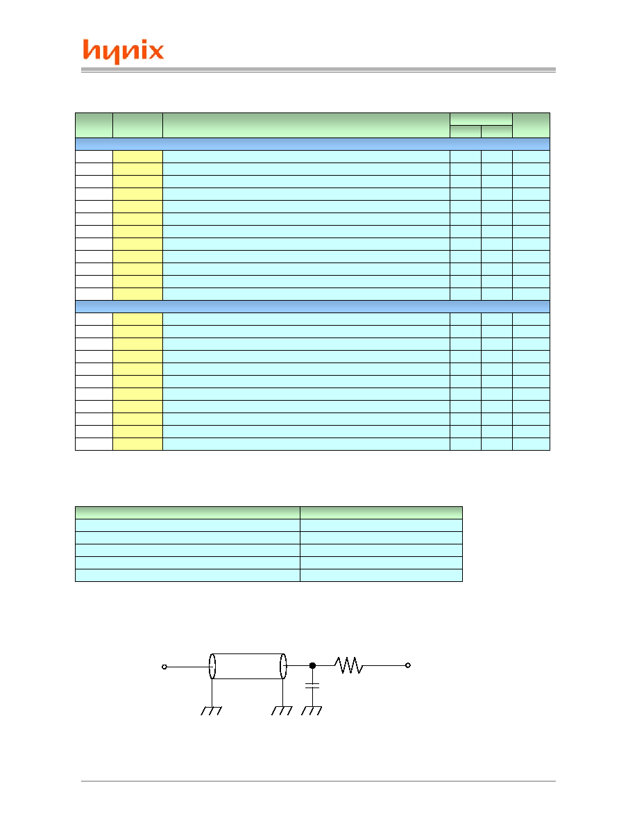
AC TEST LOADS
Note
1. Including jig and scope capacitance.
AC CHARACTERISTICS
C
L
1
=50 pF
D
OUT
R
L
=50 Ohm
V
L
=0.5*Vddq
Z
0
=50 Ohm
AC TEST CONDITIONS
T
A =
-25
∞C to 85∞C(E) / -40∞C to 85∞C(I), unless otherwise specified
Parameter
Value
Input Pulse Level
0.4V to 2.2V
Input Rising and Fall Time
5ns
Input Timing Reference Level
1.5V
Output Load
See Below
Output Timing Reference Level
0.5*Vddq
Vdd=2.7V~3.3V, Vddq=2.7V~3.3V, T
A =
-25
∞C to 85∞C(E) / -40∞C to 85∞C(I), unless otherwise specified
#
Parameter
1
Read Cycle Time
Unit
ns
Symbol
tRC
Read Cycle
2
Address Access Time
ns
tAA
3
Chip Select Access Time
ns
tACS
4
Output Enable to Output Valid
ns
tOE
5
/LB, /UB Access Time
ns
tBA
6
Chip Select to Output in Low Z
ns
tCLZ
7
Output Enable to Output in Low Z
ns
tOLZ
8
/LB, /UB Enable to Output in Low Z
ns
tBLZ
9
Chip Disable to Output in High Z
ns
tCHZ
10
Out Disable to Output in High Z
ns
tOHZ
11
/LB, /UB Disable to Output in High Z
ns
tBHZ
12
Output Hold from Address Change
ns
tOH
13
Write Cycle Time
ns
tWC
Write Cycle
14
Chip Selection to End of Write
ns
tCW
15
Address Valid to End of Write
ns
tAW
16
/LB, /UB Valid to End of Write
ns
tBW
17
Address Set-up Time
ns
tAS
18
Write Pulse Width
ns
tWP
19
Write Recovery Time
ns
tWR
20
Write to Output in High Z
ns
tWHZ
21
Data to Write Time Overlap
ns
tDW
22
Data Hold from Write Time
ns
tDH
23
Output Active from End of Write
ns
tOW
Min.
70
Max.
-
-
70
-
70
-
20
-
70
10
-
5
-
10
-
0
10
0
10
0
10
5
-
70
-
60
-
60
-
60
-
0
-
50
-
0
-
0
20
30
-
0
-
5
-
-70
HY64UD16322A Series
6
Revision 1.1
May. 2003
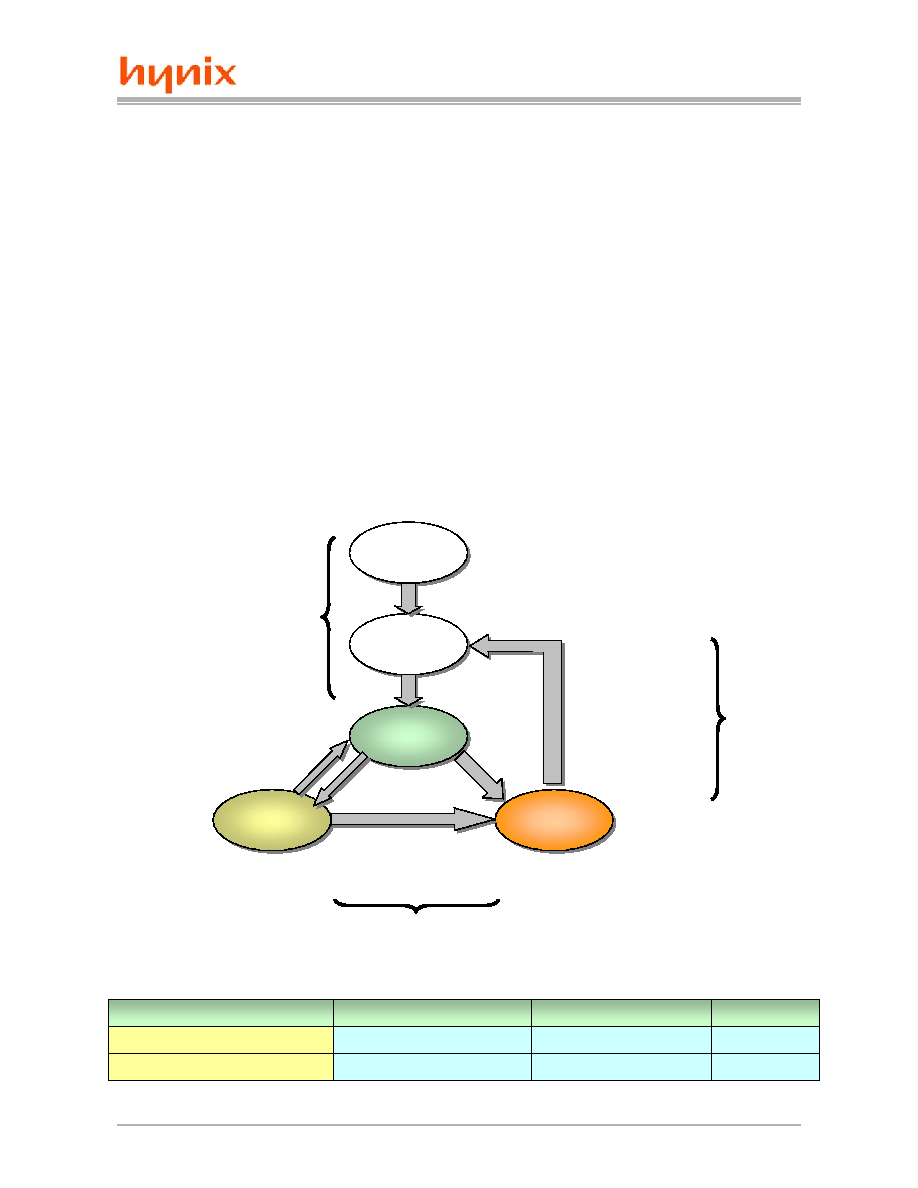
STANDBY MODE CHARACTERISTICS
STATE DIAGRAM
1. Supply power with CS2 high.
2. Maintain stable power for longer than 200
µs.
Power-Up Sequence
1. Keep CS2 low state.
Deep power down mode is maintained while CS2 is low state.
Deep Power Down Entry Sequence
1. Keep CS2 high state.
2. Maintain stable power for longer than 200
µs.
Deep Power Down Exit Sequence
Power On
Power On
Power On
Wait 200
µs
Wait 200
Wait 200
µ
µ
s
s
Active
Active
Active
Standby
Mode
Standby
Standby
Mode
Mode
Deep Power
Down Mode
Deep Power
Deep Power
Down Mode
Down Mode
/ CS1=V
IL
, CS2=V
IH
,
/UB&/LB
V
IH
CS2=V
IL
CS2=V
IL
Pow
e
r-Up
Seq
u
ence
CS2=V
IH
, /CS1=V
IH
or /UB,/LB=V
IH
Deep Pow
e
r Dow
n
Exit
Seq
u
ence
Deep Power Down
Entry Sequence
CS2=V
IH
Mode
Memory Cell Data
Standby Current[
µA]
Wait Time[
µs]
Standby
Valid
100 / 70ns
0
Deep Power Down
Invalid
2
200

HY64UD16322A Series
7
Revision 1.1
May. 2003
Notes :
1. Read Cycle occurs whenever a high on the /WE and /OE is low, while /UB and/or /LB and /CS1 and CS2 are in active status.
2. /OE = V
IL
3. tCHZ, tBHZ and tOHZ are defined as the time at which the outputs achieve the high impedance state and tOLZ,tBLZ and tCLZ
are defined as the time at which the outputs achieve the low impedance state.
These are not referenced to output voltage levels.
4. /CS1 in high for the standby, low for active.
/UB and /LB in high for the standby, low for active.
TIMING DIAGRAM
READ CYCLE 1 ( Note 1, 4 )
ADD
/CS1
CS2
/UB, /LB
/OE
Data Out
High-Z
Vih
tRC
tAA
tACS
tBA
tOE
tOLZ
(3)
tBLZ
(3)
tCLZ
(3)
tOH
tCHZ
(3)
tBHZ
(3)
tOHZ
(3)
Data Valid
READ CYCLE 2 ( Note 1, 2, 4 )( CS2=Vih )
ADD
Data Out
Data Valid
tRC
Previous Data
tOH
tAA
tOH
READ CYCLE 3 ( Note 1, 2, 4 )( CS2=Vih )
/CS1
/UB, /LB
Data Out
Data Valid
High-Z
tCLZ
(3)
tACS
tCHZ
(3)

HY64UD16322A Series
8
Revision 1.1
May. 2003
Notes :
1. A write occurs during the overlap of low /CS1, low /WE and low /UB and/or /LB.
2. tWR is measured from the earlier of /CS1, /LB, /UB, or /WE going high to the end of write cycle.
3. During this period, I/O pins are in the output state so that the input signals of opposite phase to the output must not be applied.
4. If the /CS1, /LB and /UB low transition occur simultaneously with the /WE low transition or after the
/WE transition, outputs remain in a high impedance state.
5. /OE is continuously low (/OE=V
IL
)
6. Q(data out) is the invalid data.
7. Q(data out) is the read data of the next address.
8. tWHZ is defined as the time at which the outputs achieve the high impedance state.
It is not referenced to output voltage levels.
9. /CS1 in high for the standby, low for active. /UB and /LB in high for the standby, low for active.
10. Do not input data to the I/O pins while they are in the output state.
WRITE CYCLE 1 ( Note 1, 4, 5, 9, 10 ) ( /WE Controlled )
ADD
/CS1
CS2
/UB, /LB
/WE
Data Out
Data In
Vih
tWC
tCW
tBW
tWP
tWR
(2)
Data Valid
tAW
tAS
High-Z
tDW
tDH
tWHZ
(3,8)
tOW
(6)
(7)
WRITE CYCLE 2 ( Note 1, 4, 5, 9, 10 ) ( /CS1 Controlled )
ADD
/CS1
CS2
/UB, /LB
/WE
Data Out
Data In
Vih
tWC
tCW
tBW
tWP
tWR
(2)
Data Valid
tAW
High-Z
tDW
tDH
High-Z
tAS

HY64UD16322A Series
9
Revision 1.1
May. 2003
AVOID TIMING
/WE
/CS1
ADD
< tRC
10us
ABNORMAL TIMING
/WE
/CS1
ADD
tRC
10us
AVOIDABLE TIMING(1)
Hynix 1T/1C SRAM has a timing which is not supported at read operation. If your system has multiple
invalid address signal shorter than tRC during over 10us at read operation which showed in abnormal
timing, Hynix 1T/1C SRAM needs a normal read timing at least during 10us which showed in avoidable
timing(1) or toggle the /CS1 to high(
tRC) one time at least which showed in avoidable timing(2)
/WE
/CS1
ADD
10us
tRC
AVOIDABLE TIMING(2)
< tRC

HY64UD16322A Series
10
Revision 1.1
May. 2003
NOTE.
1. DIMENSIONING AND TOLERANCING PER ASME Y14.5M-1994.
2. ALL DIMENSIONS ARE MILLIMETERS.
3. DIMENSION "D" IS MEASURED AT THE MAXIMUM SOLDER
BALL DIAMETER IN A PLANE PARALLEL TO DATUM C.
4. PRIMARY DATUM C(SEATING PLANE) IS DEFINED BY THE
CROWN OF THE SOLDER BALLS.
5. THIS IS A CONTROLLING DIMENSION.
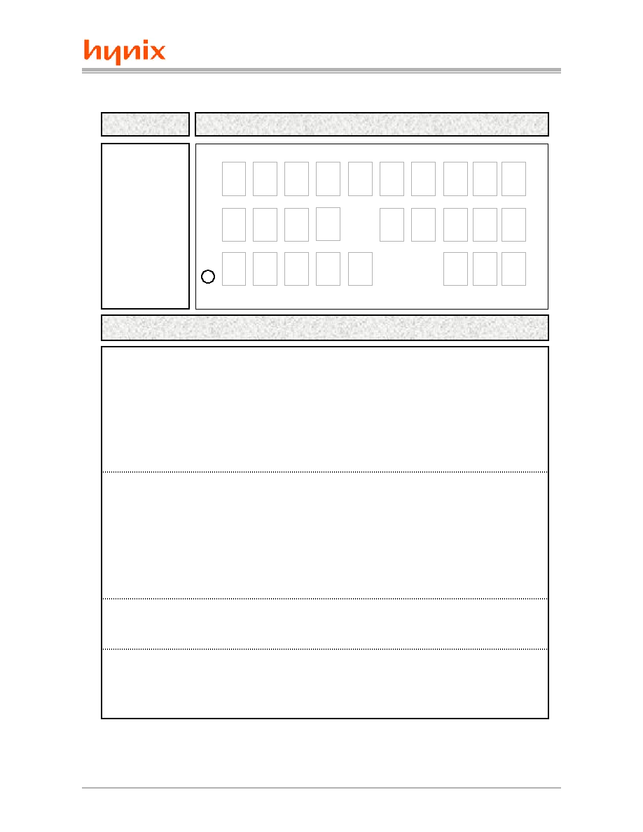
PACKAGE DIMENSION
NOTE.
1. DIMENSIONING AND TOLERANCING PER ASME Y14.5M-1994.
2. ALL DIMENSIONS ARE MILLIMETERS.
3. DIMENSION "D" IS MEASURED AT THE MAXIMUM SOLDER
BALL DIAMETER IN A PLANE PARALLEL TO DATUM C.
4. PRIMARY DATUM C(SEATING PLANE) IS DEFINED BY THE
CROWN OF THE SOLDER BALLS.
5. THIS IS A CONTROLLING DIMENSION.
48ball Fine Pitch Ball Grid Array Package(F)
unit : mm
A
A
B1
B1
B
B
C1
C1
C
C
D
D
E
E
E1
E1
E2
E2
R
R
Symbol
-
-
-
-
5
5
.90
.90
-
-
7
7
.90
.90
0.
0.
3
3
0
0
-
-
-
-
0.20
0.20
-
-
Min.
0.75
0.75
3.75
3.75
6
6
.00
.00
5.25
5.25
8
8
.00
.00
0.
0.
3
3
5
5
1.00
1.00
0.75
0.75
0.25
0.25
-
-
Typ.
-
-
-
-
6
6
.10
.10
-
-
8
8
.10
.10
0.
0.
4
4
0
0
1.10
1.10
-
-
0.30
0.30
0.08
0.08
Max.
B
B
C
C
TOP VIEW
TOP VIEW
A1 CORNER
A1 CORNER
INDEX AREA
INDEX AREA
E
E
E2
E2
SIDE VIEW
SIDE VIEW
C
C
A
A
5
5
R
R
D(DIAMETER)
D(DIAMETER)
3
3
E1
E1
SEATING PLANE
SEATING PLANE
4
4
A
A
B1
B1
C1
C1
BOTTOM VIEW
BOTTOM VIEW
A
A
B
B
C
C
D
D
E
E
F
F
G
G
H
H
6
6
5
5
4
4
3
3
2
2
1
1
A
A
C/2
C/2
B/2
B/2
A1 INDEX
A1 INDEX
MARK
MARK
HY64UD16322A Series
11
Revision 1.1
May. 2003
MARKING INFORMATION
Index
∑ HYUD16322A
: Part Name
HY
: HYNIX
U
: Power Supply
: Vdd=2.7V~3.3V
/
Vddq=2.7V~3.3V
D
: Tech. + Classification
: 1T+1C
16
: Bit Organization
: x16
32
: Density
: 32M
2
: Mode
: 1CS with /UB,/LB;tCS
A
: Version
: 2nd Generation
∑ c
: Power Consumption
: D ≠ Low Low Power
∑ ss
: Speed
: 70 ≠ 70ns
∑ t
: Temperature
: E ≠ Extended(-25 ~ 85
∞C)
I ≠ Industrial(-40 ~ 85
∞C)
∑ yy
: Year (ex : 02 = year 2002, 03= year 2003)
∑ ww
: Work Week ( ex : 12 = work week 12 )
∑ p
: Process Code : B
∑ xxxxx
: Lot No.
∑ KOR
: Origin Country
Note
- Capital Letter
: Fixed Item
- Small Letter
: Non-fixed Item
Package
Marking Example
FBGA
H
Y
U
D
1
6
3
2
2
A
c
s
s
t
y
y
w
w
p
x
x
x
x
x
K
O
R