16Mx72 bits
PC133 SDRAM Unbuffered DIMM
based on 16Mx8 SDRAM with LVTTL, 4 banks & 4K Refresh
This document is a general product description and is subject to change without notice. Hynix Semiconductor Inc. does not assume any responsibility for
use of circuits described. No patent licenses are implied.
Rev. 0.5/Dec. 01 2
HYM71V16735AT8M Series
DESCRIPTION
The Hynix HYM71V16735AT8M Series are 16Mx72bits ECC Synchronous DRAM Modules. The modules are composed of nine
16Mx8bits CMOS Synchronous DRAMs in 400mil 54pin TSOP-II package, one 2Kbit EEPROM in 8pin TSSOP package on a 168pin
glass-epoxy printed circuit board. One 0.0022uF decoupling capacitors per each SDRAM are mounted on the PCB.
The Hynix HYM71V16735AT8M Series are Dual In-line Memory Modules suitable for easy interchange and addition of 128Mbytes
memory. The Hynix HYM71V16735AT8M Series are fully synchronous operation referenced to the positive edge of the clock . All
inputs and outputs are synchronized with the rising edge of the clock input. The data paths are internally pipelined to achieve very high
bandwidth.
FEATURES
∑
PC133/PC100MHz support
∑
168pin SDRAM Unbuffered DIMM
∑
Serial Presence Detect with EEPROM
∑
1.155" (29.34mm) Height PCB with single sided
components
∑
Single 3.3
±
0.3V power supply
∑
All device pins are compatible with LVTTL interface
∑
Data mask function by DQM
∑
SDRAM internal banks : four banks
∑
Module bank : one physical bank
∑
Auto refresh and self refresh
∑
4096 refresh cycles / 64ms
∑
Programmable Burst Length and Burst Type
- 1, 2, 4 or 8 or Full page for Sequential Burst
- 1, 2, 4 or 8 for Interleave Burst
∑
Programmable CAS Latency ; 2, 3 Clocks
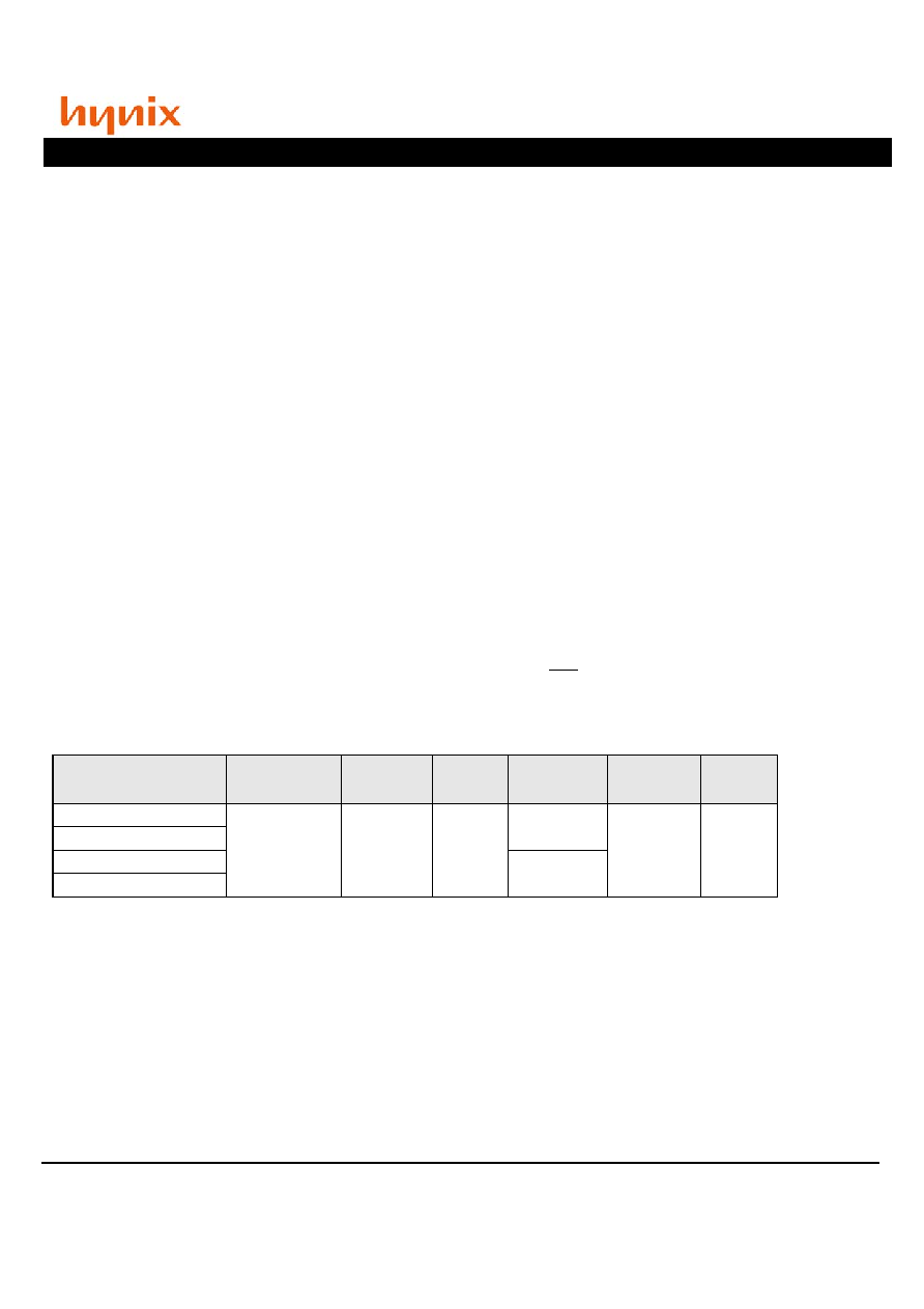
ORDERING INFORMATION
Part No.
Clock
Frequency
Internal
Bank
Ref.
Power
SDRAM
Package
Plating
HYM71V16735AT8M-K
133MHz
4 Banks
4K
Normal
TSOP-II
Gold
HYM71V16735AT8M-H
HYM71V16735ALT8M-K
Low Power
HYM71V16735ALT8M-H

PC133 SDRAM Unbuffered DIMM
Rev. 0.5/Dec. 01 3
HYM71V16735AT8M Series
PIN DESCRIPTION
PIN
PIN NAME
DESCRIPTION
CK0~CK3
Clock Inputs
The system clock input. All other inputs are registered to the SDRAM on the
rising edge of CLK
CKE0
Clock Enable
Controls internal clock signal and when deactivated, the SDRAM will be one
of the states among power down, suspend or self refresh
/S0, /S2
Chip Select
Enables or disables all inputs except CK, CKE and DQM
BA0, BA1
SDRAM Bank Address
Selects bank to be activated during /RAS activity
Selects bank to be read/written during /CAS activity
A0 ~ A11
Address
Row Address : RA0 ~ RA11, Column Address : CA0 ~ CA9
Auto-precharge flag : A10
/RAS, /CAS, /WE
Row Address Strobe, Column
Address Strobe, Write Enable
/RAS, /CAS and /WE define the operation
Refer function truth table for details
DQM0~DQM7
Data Input/Output Mask
Controls output buffers in read mode and masks input data in write mode
DQ0 ~ DQ63
Data Input/Output
Multiplexed data input / output pin
CB0 ~ CB7
Check Bit Input/Output
Check bits for ECC
VCC
Power Supply (3.3V)
Power supply for internal circuits and input buffers
V
SS
Ground
Ground
SCL
SPD Clock Input
Serial Presence Detect Clock input
SDA
SPD Data Input/Output
Serial Presence Detect Data input/output
SA0~2
SPD Address Input
Serial Presence Detect Address Input
WP
Write Protect for SPD
Write Protect for Serial Presence Detect on DIMM
NC
No Connection
No connection

PC133 SDRAM Unbuffered DIMM
Rev. 0.5/Dec. 01 4
HYM71V16735AT8M Series
PIN ASSIGNMENTS
FRONT SIDE
BACK SIDE
FRONT SIDE
BACK SIDE
PIN NO.
NAME
PIN NO.
NAME
PIN NO.
NAME
PIN NO.
NAME
1
VSS
85
VSS
41
VCC
125
*CK1
2
DQ0
86
DQ32
42
CK0
126
NC
3
DQ1
87
DQ33
43
VSS
127
VSS
4
DQ2
88
DQ34
44
NC
128
CKE0
5
DQ3
89
DQ35
45
/S2
129
NC
6
VCC
90
VCC
46
DQM2
130
DQM6
7
DQ4
91
DQ36
47
DQM3
131
DQM7
8
DQ5
92
DQ37
48
NC
132
NC
9
DQ6
93
DQ38
49
VCC
133
VCC
10
DQ7
94
DQ39
50
NC
134
NC
Architecture Key
51
NC
135
NC
52
CB2
136
CB6
11
DQ8
95
DQ40
53
CB3
137
CB7
12
VSS
96
VSS
54
VSS
138
VSS
13
DQ9
97
DQ41
55
DQ16
139
DQ48
14
DQ10
98
DQ42
56
DQ17
140
DQ49
15
DQ11
99
DQ43
57
DQ18
141
DQ50
16
DQ12
100
DQ44
58
DQ19
142
DQ51
17
DQ13
101
DQ45
59
VCC
143
VCC
18
VCC
102
VCC
60
DQ20
144
DQ52
19
DQ14
103
DQ46
61
NC
145
NC
20
DQ15
104
DQ47
62
NC
146
NC
21
CB0
105
CB4
63
NC
147
NC
22
CB1
106
CB5
64
VSS
148
VSS
23
VSS
107
VSS
65
DQ21
149
DQ53
24
NC
108
NC
66
DQ22
150
DQ54
25
NC
109
NC
67
DQ23
151
DQ55
26
VCC
110
VCC
68
VSS
152
VSS
27
/WE
111
/CAS
69
DQ24
153
DQ56
28
DQM0
112
DQM4
70
DQ25
154
DQ57
29
DQM1
113
DQM5
71
DQ26
155
DQ58
30
/S0
114
NC
72
DQ27
156
DQ59
31
NC
115
/RAS
73
VCC
157
VCC
32
VSS
116
VSS
74
DQ28
158
DQ60
33
A0
117
A1
75
DQ29
159
DQ61
34
A2
118
A3
76
DQ30
160
DQ62
35
A4
119
A5
77
DQ31
161
DQ63
36
A6
120
A7
78
VSS
162
VSS
37
A8
121
A9
79
CK2
163
*CK3
38
A10/AP
122
BA0
80
NC
164
NC
39
BA1
123
A11
81
WP
165
SA0
40
VCC
124
VCC
82
SDA
166
SA1
Voltage Key
83
SCL
167
SA2
84
VCC
168
VCC
Note : * CK1, CK3 are connected with termination R/C (Refer to the Block Diagram)

PC133 SDRAM Unbuffered DIMM
Rev. 0.5/Dec. 01 5
HYM71V16735AT8M Series
BLOCK DIAGRAM
Note : 1. The serial resistor values of DQs are 10ohms
2. The padding capacitance of termination R/C for CK1,CK3 is 10pF

PC133 SDRAM Unbuffered DIMM
Rev. 0.5/Dec. 01 6
HYM71V16735AT8M Series
SERIAL PRESENCE DETECT
BYTE
NUMBER
FUNCTION
DESCRIPTION
FUNCTION
VALUE
NOTE
-K
-H
-K
-H
BYTE0
# of Bytes Written into Serial Memory at Module
Manufacturer
128 Bytes
80h
BYTE1
Total # of Bytes of SPD Memory Device
256 Bytes
08h
BYTE2
Fundamental Memory Type
SDRAM
04h
BYTE3
# of Row Addresses on This Assembly
12
0Ch
1
BYTE4
# of Column Addresses on This Assembly
10
0Ah
BYTE5
# of Module Banks on This Assembly
1 Bank
01h
BYTE6
Data Width of This Assembly
72 Bits
48h
BYTE7
Data Width of This Assembly (Continued)
-
00h
BYTE8
Voltage Interface Standard of This Assembly
LVTTL
01h
BYTE9
SDRAM Cycle Time @/CAS Latency=3
7.5ns
7.5
75h
75h
BYTE10
Access Time from Clock @/CAS Latency=3
5.4ns
5.4
54h
54h
BYTE11
DIMM Configuration Type
ECC
02h
BYTE12
Refresh Rate/Type
15.625us
/ Self Refresh Supported
80h
BYTE13
Primary SDRAM Width
x8
08h
BYTE14
Error Checking SDRAM Width
x8
08h
BYTE15
Minimum Clock Delay Back to Back Random Column
Address
tCCD = 1 CLK
01h
BYTE16
Burst Lenth Supported
1,2,4,8,Full Page
8Fh
2
BYTE17
# of Banks on Each SDRAM Device
4 Banks
04h
BYTE18
SDRAM Device Attributes, /CAS Lataency
/CAS Latency=2,3
06h
BYTE19
SDRAM Device Attributes, /CS Lataency
/CS Latency=0
01h
BYTE20
SDRAM Device Attributes, /WE Lataency
/WE Latency=0
01h
BYTE21
SDRAM Module Attributes
Neither Buffered nor Registered
00h
BYTE22
SDRAM Device Attributes, General
+/- 10% voltage tolerence,
Burst Read Single Bit Write,
Precharge All, Auto Precharge,
Early RAS Precharge
0Eh
BYTE23
SDRAM Cycle Time @/CAS Latency=2
7.5ns
10ns
75h
A0h
BYTE24
Access Time from Clock @/CAS Latency=2
5.4ns
6ns
54h
60h
BYTE25
SDRAM Cycle Time @/CAS Latency=1
-
-
00h
00h
BYTE26
Access Time from Clock @/CAS Latency=1
-
-
00h
00h
BYTE27
Minimum Row Precharge Time (tRP)
15ns
20ns
0Fh
14h
BYTE28
Minimum Row Active to Row Active Delay (tRRD)
15ns
15ns
0Fh
0Fh
BYTE29
Minimum /RAS to /CAS Delay (tRCD)
15ns
20ns
0Fh
14h
BYTE30
Minimum /RAS Pulse Width (tRAS)
45ns
45ns
2Dh
2Dh
BYTE31
Module Bank Density
128MB
20h
BYTE32
Command and Address Signal Input Setup Time
1.5ns
1.5ns
15h
15h
BYTE33
Command and Address Signal Input Hold Time
0.8ns
0.8ns
08h
08h
BYTE34
Data Signal Input Setup Time
1.5ns
1.5ns
15h
15h
BYTE35
Data Signal Input Hold Time
0.8ns
0.8ns
08h
08h
BYTE36
~61
Superset Information (may be used in future)
-
00h
BYTE62
SPD Revision
Intel SPD 1.2B
12h
3, 8
BYTE63
Checksum for Byte 0~62
-
80
C1h
BYTE64
Manufacturer JEDEC ID Code
Hynix JEDED ID
ADh
BYTE65
~71
....Manufacturer JEDEC ID Code
Unused
FFh
BYTE72
Manufacturing Location
HSI (Korea Area)
HSA (United States Area)
HSE (Europe Area)
HSJ (Japan Area)
HSS(Singapore)
Asia Area
0*h
1*h
2*h
3*h
4*h
5*h
10

PC133 SDRAM Unbuffered DIMM
Rev. 0.5/Dec. 01 7
HYM71V16735AT8M Series
BYTE
NUMBER
FUNCTION
DESCRIPTION
FUNCTION
VALUE
NOTE
-K
-H
-K
-H
BYTE73
Manufacturer's Part Number (Component)
7 (SDRAM)
37h
4, 5
BYTE74
Manufacturer's Part Number (128Mb based)
1
31h
4, 5
BYTE75
Manufacturer's Part Number (Voltage Interface)
V (3.3V, LVTTL)
56h
4, 5
BYTE76
Manufacturer's Part Number (Memory Width)
1
31h
4, 5
BYTE77
....Manufacturer's Part Number (Memory Width)
6
36h
4, 5
BYTE78
Manufacturer's Part Number (Data Width)
7
37h
4, 5
BYTE79
....Manufacturer's Part Number (Data Width)
3
33h
4, 5
BYTE80
Manufacturer's Part Number (Refresh, SDRAM Bank)
5 (4K Refresh, 4Banks)
35h
4, 5
BYTE81
Manufacturer's Part Number (Generation)
A
41h
4, 5
BYTE82
Manufacturer's Part Number (Package Type)
T
54h
4, 5
BYTE83
Manufacturer's Part Number (Component Configuration)
8 (x8 based)
38h
4, 5
BYTE84
Manufacturer's Part Number (Module Revision)
M(1st Revision)
4Dh
4, 5
BYTE85
Manufacturer's Part Number (Hyphent)
- (Hyphen)
2Dh
4, 5
BYTE86
Manufacturer's Part Number (Min. Cycle Time)
K
H
4Bh
48h
4, 5
BYTE87
~90
Manufacturer's Part Number
Blanks
20h
4, 5
BYTE91
Revision Code (for Component)
Process Code
-
4, 6
BYTE92
....Revision Code (for PCB)
Process Code
-
4, 6
BYTE93
Manufacturing Date
Year
-
3, 6
BYTE94
....Manufacturing Date
Work Week
-
3, 6
BYTE95
~98
Assembly Serial Number
Serial Number
-
6
BYTE99
~125
Manufacturer Specific Data (may be used in future)
None
00h
BYTE126
Reserved
100MHz
64h
7, 8, 9
BYTE127
Reserved
Refer to Note7
AFh
7, 8, 9
BYTE128
~256
Unused Storage Locations
-
00h
Continued
Note :
1. The bank address is excluded
2. 1, 2, 4, 8 for Interleave Burst Type
3. BCD adopted
4. ASCII adopted
5. Basically Hynix writes Part No. except for `HYM' in Byte 73~90 to use the limited 18 bytes from byte 73 to byte 90
6. Not fixed but dependent
7. CK0, CK2 connected to DIMM, TBD junction temp, CL2(3) support, Intel defined Concurrent Auto Precharge suport
8. Refer to the most recent Intel and JEDEC SPD Specification
9. These values are applied to PC100 applications only per Intel PC SDRAM specification
10. Refer to HSI Web site.

PC133 SDRAM Unbuffered DIMM
Rev. 0.5/Dec. 01 8
HYM71V16735AT8M Series
ABSOLUTE MAXIMUM RATINGS
Note : Operation at above absolute maximum rating can adversely affect device reliability.
DC OPERATING CONDITION
(T
A
=0 to 70
∞
C)
Note :
1.All voltages are referenced to V
SS
= 0V
2.V
IH
(max) is acceptable 5.6V AC pulse width with <=3ns of duration.
3.V
IL
(min) is acceptable -2.0V AC pulse width with <=3ns of duration.
AC OPERATING TEST CONDITION
(T
A
=0 to 70
∞
C, V
DD
=3.3
±
0.3V, V
SS
=0V)
Note :
1.Output load to measure access times is equivalent to two TTL gates and one capacitor (50pF). For details, refer to AC/DC output
load circuit
Parameter
Symbol
Rating
Unit
Ambient Temperature
T
A
0 ~ 70
∞
C
Storage Temperature
T
STG
-55 ~ 125
∞
C
Voltage on Any Pin relative to V
SS
V
IN
, V
OUT
-1.0 ~ 4.6
V
Voltage on V
DD
relative to V
SS
V
DD,
V
DDQ
-1.0 ~ 4.6
V
Short Circuit Output Current
I
OS
50
mA
Power Dissipation
P
D
9
W
Soldering Temperature
Time
T
SOLDER
260
10
∞
C
Sec
Parameter
Symbol
Min
Typ
Max
Unit
Note
Power Supply Voltage
V
DD
, V
DDQ
3.0
3.3
3.6
V
1
Input High voltage
V
IH
2.0
3.0
V
DDQ
+ 0.3
V
1,2
Input Low voltage
V
IL
-0.3
0
0.8
V
1,3
Parameter
Symbol
Value
Unit
Note
AC Input High / Low Level Voltage
V
IH
/ V
IL
2.4/0.4
V
Input Timing Measurement Reference Level Voltage
Vtrip
1.4
V
Input Rise / Fall Time
tR / tF
1
ns
Output Timing Measurement Reference Level Voltage
Voutref
1.4
V
Output Load Capacitance for Access Time Measurement
C
L
50
pF
1
PC133 SDRAM Unbuffered DIMM
Rev. 0.5/Dec. 01 9
HYM71V16735AT8M Series
CAPACITANCE
(TA=25
∞
C, f=1MHz)
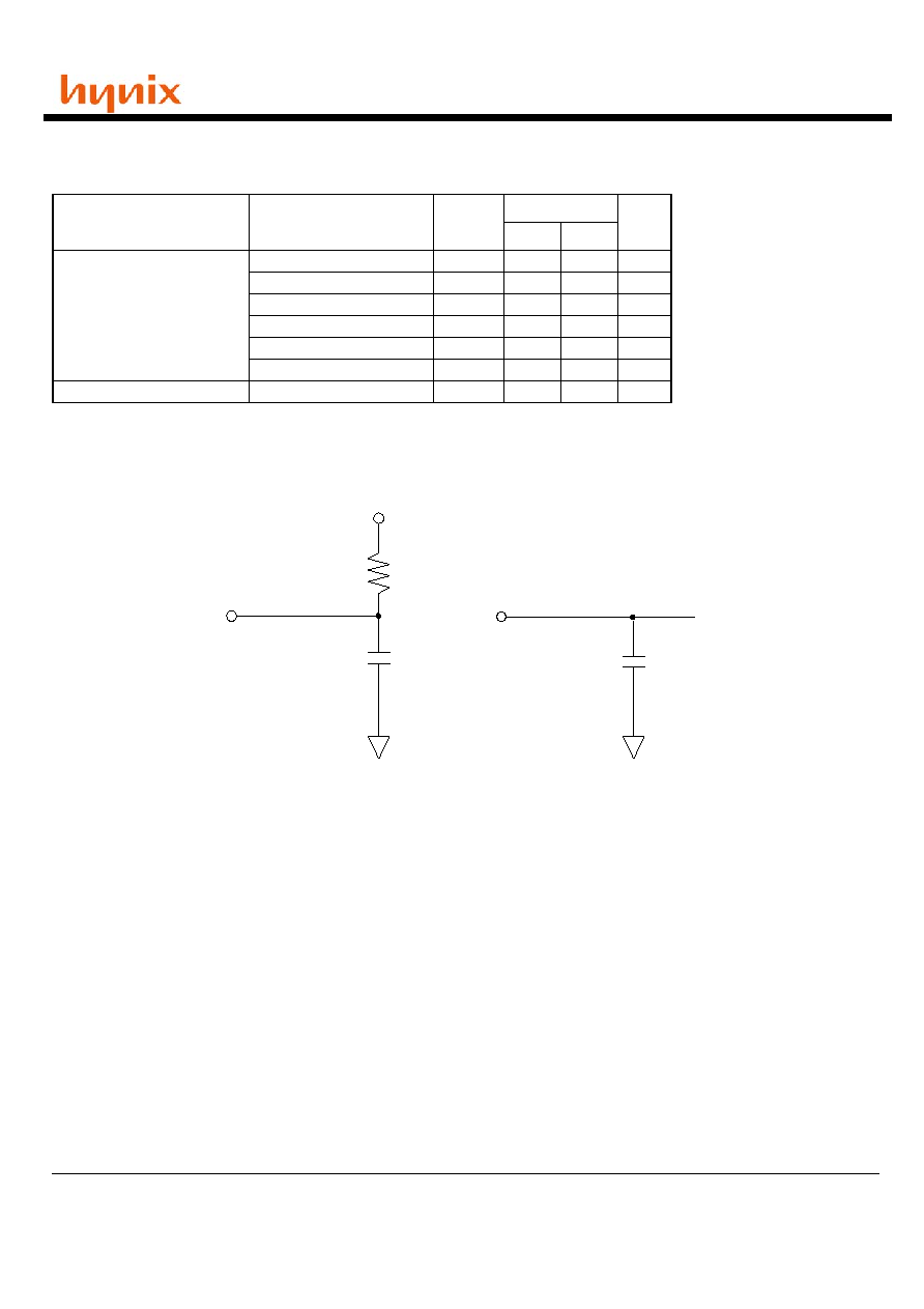
OUTPUT LOAD CIRCUIT
Parameter
Pin
Symbol
-K/H
Unit
Min
Max
Input Capacitance
CK0, CK2
C
I1
25
40
pF
CKE0
C
I2
35
55
pF
/S0, /S2
C
I3
20
35
pF
A0~11, BA0, BA1
C
I4
35
60
pF
/RAS, /CAS, /WE
C
I5
35
60
pF
DQM0~DQM7
CI
6
10
20
pF
Data Input / Output Capacitance
DQ0 ~ DQ63
C
I/O
6
15
pF
Vtt=1.4V
RT=250
50pF
Output
50pF
Output
DC Output Load Circuit
AC Output Load Circuit

PC133 SDRAM Unbuffered DIMM
Rev. 0.5/Dec. 01 10
HYM71V16735AT8M Series
DC CHARACTERISTICS I
(TA=0 to 70
∞
C, V
DD
=3.3
±
0.3V)
Note :
1.V
IN
= 0 to 3.6V, All other pins are not tested under V
IN
=0V
2.D
OUT
is disabled, V
OUT
=0 to 3.6
DC CHARACTERISTICS II
Note :
1. I
DD1
and I
DD4
depend on output loading and cycle rates. Specified values are measured with the output open
2. Min. of tRRC (Refresh RAS cycle time) is shown at AC CHARACTERISTICS II
3.HYM71V16735AT8M-H
4.HYM71V16735ALT8M-H
Parameter
Symbol
Min.
Max
Unit
Note
Input Leakage Current
I
LI
-9
9
uA
1
Output Leakage Current
I
LO
-1
1
uA
2
Output High Voltage
V
OH
2.4
-
V
I
OH
= -4mA
Output Low Voltage
V
OL
-
0.4
V
I
OL
= +4mA
Parameter
Symbol
Test Condition
Speed
Unit
Note
-K
-H
Operating Current
I
DD1
Burst length=1, One bank active
t
RC
t
RC
(min), I
OL
=0mA
1080
990
mA
1
Precharge Standby Current
in Power Down Mode
I
DD2P
CKE
V
IL
(max), t
CK
= 15ns
18
mA
I
DD2PS
CKE
V
IL
(max), t
CK
=
18
Precharge Standby Current
in Non Power Down Mode
I
DD2N
CKE
V
IH
(min), CS
V
IH
(min), t
CK
= 15ns
Input signals are changed one time during
30ns. All other pins
V
DD
-0.2V or
0.2V
180
mA
I
DD2NS
CKE
V
IH
(min), t
CK
=
Input signals are stable.
90
Active Standby Current
in Power Down Mode
I
DD3P
CKE
V
IL
(max), t
CK
= 15ns
63
mA
I
DD3PS
CKE
V
IL
(max), t
CK
=
63
Active Standby Current
in Non Power Down Mode
I
DD3N
CKE
V
IH
(min), CS
V
IH
(min), t
CK
= 15ns
Input signals are changed one time during
30ns. All other pins
V
DD
-0.2V or
0.2V
360
mA
I
DD3NS
CKE
V
IH
(min), t
CK
=
Input signals are stable.
360
Burst Mode Operating
Current
I
DD4
t
CK
t
CK
(min), I
OL
=0mA
All banks active
CL=3
1080
1080
mA
1
CL=2
1080
900
Auto Refresh Current
I
DD5
t
RRC
t
RRC
(min), All banks active
2160
mA
2
Self Refresh Current
I
DD6
CKE
0.2V
18
mA
3
Burst length=1, One bank active
t
RC
t
RC
(min), I
OL
=0mA
7.2
mA
4

PC133 SDRAM Unbuffered DIMM
Rev. 0.5/Dec. 01 11
HYM71V16735AT8M Series
AC CHARACTERISTICS I
(AC operating conditions unless otherwise noted)
Note :
1.Assume tR / tF (input rise and fall time ) is 1ns
If tR & tF > 1ns, then [(tR+tF)/2-1]ns should be added to the parameter
2.Access times to be measured with input signals of 1v/ns edge rate, from 0.8v to 2.0v
If tR > 1ns, then (tR/2-0.5)ns should be added to the parameter
Parameter
Symbol
-K
-H
Unit
Note
Min
Max
Min
Max
System Clock
Cycle Time
CAS Latency = 3
tCK3
7.5
1000
7.5
1000
ns
CAS Latency = 2
tCK2
7.5
10
ns
Clock High Pulse Width
tCHW
2.5
-
2.5
-
ns
1
Clock Low Pulse Width
tCLW
2.5
-
2.5
-
ns
1
Access Time
From Clock
CAS Latency = 3
tAC3
-
5.4
-
5.4
ns
2
CAS Latency = 2
tAC2
-
5.4
-
6
ns
Data-Out Hold Time
tOH
2.7
-
2.7
-
ns
Data-Input Setup Time
tDS
1.5
-
1.5
-
ns
1
Data-Input Hold Time
tDH
0.8
-
0.8
-
ns
1
Address Setup Time
tAS
1.5
-
1.5
-
ns
1
Address Hold Time
tAH
0.8
-
0.8
-
ns
1
CKE Setup Time
tCKS
1.5
-
1.5
-
ns
1
CKE Hold Time
tCKH
0.8
-
0.8
-
ns
1
Command Setup Time
tCS
1.5
-
1.5
-
ns
1
Command Hold Time
tCH
0.8
-
0.8
-
ns
1
CLK to Data Output in Low-Z Time
tOLZ
1
-
1
-
ns
CLK to Data
Output in High-Z
Time
CAS Latency = 3
tOHZ3
2.7
5.4
2.7
5.4
ns
CAS Latency = 2
tOHZ2
2.7
5.4
3
6
ns

PC133 SDRAM Unbuffered DIMM
Rev. 0.5/Dec. 01 12
HYM71V16735AT8M Series
AC CHARACTERISTICS II
Note :
1. A new command can be given tRRC after self refresh exit
Parameter
Symbol
-K
-H
Unit
Note
Min
Max
Min
Max
RAS Cycle Time
Operation
tRC
60
-
65
-
ns
Auto Refresh
tRRC
60
-
65
-
ns
RAS to CAS Delay
tRCD
15
-
20
-
ns
RAS Active Time
tRAS
45
100K
45
100K
ns
RAS Precharge Time
tRP
15
-
20
-
ns
RAS to RAS Bank Active Delay
tRRD
15
-
15
-
ns
CAS to CAS Delay
tCCD
1
-
1
-
CLK
Write Command to Data-In Delay
tWTL
0
-
0
-
CLK
Data-In to Precharge Command
tDPL
2
-
2
-
CLK
Data-In to Active Command
tDAL
4
-
5
-
CLK
DQM to Data-Out Hi-Z
tDQZ
2
-
2
-
CLK
DQM to Data-In Mask
tDQM
0
-
0
-
CLK
MRS to New Command
tMRD
2
-
2
-
CLK
Precharge to Data
Output Hi-Z
CAS Latency = 3
tPROZ3
3
-
3
-
CLK
CAS Latency = 2
tPROZ2
2
-
2
-
CLK
Power Down Exit Time
tPDE
1
-
1
-
CLK
Self Refresh Exit Time
tSRE
1
-
1
-
CLK
1
Refresh Time
tREF
-
64
-
64
ms

PC133 SDRAM Unbuffered DIMM
Rev. 0.5/Dec. 01 13
HYM71V16735AT8M Series
DEVICE OPERATING OPTION TABLE
HYM71V16735A(L)T8M-K
HYM71V16735A(L)T8M-H
CAS Latency
tRCD
tRAS
tRC
tRP
tAC
tOH
133MHz(7.5ns)
2CLKs
2CLKs
6CLKs
8CLKs
2CLKs
5.4ns
2.7ns
125MHz(8ns)
3CLKs
3CLKs
6CLKs
9CLKs
3CLKs
6ns
3ns
100MHz(10ns)
2CLKs
2CLKs
5CLKs
7CLKs
2CLKs
6ns
3ns
CAS Latency
tRCD
tRAS
tRC
tRP
tAC
tOH
133MHz(7.5ns)
3CLKs
3CLKs
6CLKs
9CLKs
3CLKs
5.4ns
2.7ns
125MHz(8ns)
3CLKs
3CLKs
6CLKs
9CLKs
3CLKs
6ns
3ns
100MHz(10ns)
2CLKs
2CLKs
5CLKs
7CLKs
2CLKs
6ns
3ns

PC133 SDRAM Unbuffered DIMM
Rev. 0.5/Dec. 01 14
HYM71V16735AT8M Series
COMMAND TRUTH TABLE
Note :
1. Exiting Self Refresh occurs by asynchronously bringing CKE from low to high
2. X = Don
t care, H = Logic High, L = Logic Low. BA =Bank Address, RA = Row Address, CA = Column Address,
Opcode = Operand Code, NOP = No Operation
3. The burst read sigle write mode is entered by programming the Write burst mode bit (A9) in the mode register to a logic 1.
Command
CKEn-1
CKEn
CS
RAS
CAS
WE
DQM
ADDR
A10/
AP
BA
Note
Mode Register Set
H
X
L
L
L
L
X
OP code
No Operation
H
X
H
X
X
X
X
X
L
H
H
H
Bank Active
H
X
L
L
H
H
X
RA
V
Read
H
X
L
H
L
H
X
CA
L
V
Read with Autoprecharge
H
Write
H
X
L
H
L
L
X
CA
L
V
Write with Autoprecharge
H
Precharge All Banks
H
X
L
L
H
L
X
X
H
X
Precharge selected Bank
L
V
Burst Stop
H
X
L
H
H
L
X
X
DQM
H
X
V
X
Auto Refresh
H
H
L
L
L
H
X
X
Burst-Read-Single-WRITE
H
X
L
L
L
L
X
A9 Pin High
(Other Pins OP code)
MRS
Mode
Self Refresh
1
Entry
H
L
L
L
L
H
X
X
Exit
L
H
H
X
X
X
X
L
H
H
H
Precharge power
down
Entry
H
L
H
X
X
X
X
X
L
H
H
H
Exit
L
H
H
X
X
X
X
L
H
H
H
Clock
Suspend
Entry
H
L
H
X
X
X
X
X
L
V
V
V
Exit
L
H
X
X

PC133 SDRAM Unbuffered DIMM
Rev. 0.5/Dec. 01 15
HYM71V16735AT8M Series
PACKAGE DEMENSION