32Mx64 bits
Unbuffered DDR SO-DIMM
This document is a general product description and is subject to change without notice. Hynix Semiconductor does not assume any
responsibility for use of circuits described. No patent licenses are implied.
Rev. 0.2/May. 02 1
HYMD232M646A(L)8-J/M/K/H/L
DESCRIPTION
Hynix HYMD232M646A(L)8-J/M/K/H/L series is unbuffered 200-pin double data rate Synchronous DRAM Small Outline
Dual In-Line Memory Modules (SO-DIMMs) which are organized as 32Mx64 high-speed memory arrays. Hynix
HYMD232M646A(L)8-J/M/K/H/L series consists of eight 32Mx8 DDR SDRAM in 400mil TSOP II packages on a 200pin
glass-epoxy substrate. Hynix HYMD232M646A(L)8-J/M/K/H/L series provide a high performance 8-byte interface in
67.60mmX 31.75mm form factor of industry standard. It is suitable for easy interchange and addition.
Hynix HYMD232M646A(L)8-J/M/K/H/L series is designed for high speed of up to 166MHz and offers fully synchronous
operations referenced to both rising and falling edges of differential clock inputs. While all addresses and control
inputs are latched on the rising edges of the clock, Data, Data strobes and Write data masks inputs are sampled on
both rising and falling edges of it. The data paths are internally pipelined and 2-bit prefetched to achieve very high
bandwidth. All input and output voltage levels are compatible with SSTL_2. High speed frequencies, programmable
latencies and burst lengths allow variety of device operation in high performance memory system.
Hynix HYMD232M646A(L)8-J/M/K/H/L series incorporates SPD(serial presence detect). Serial presence detect function
is implemented via a serial 2,048-bit EEPROM. The first 128 bytes of serial PD data are programmed by Hynix to iden-
tify DIMM type, capacity and other the information of DIMM and the last 128 bytes are available to the customer.
FEATURES
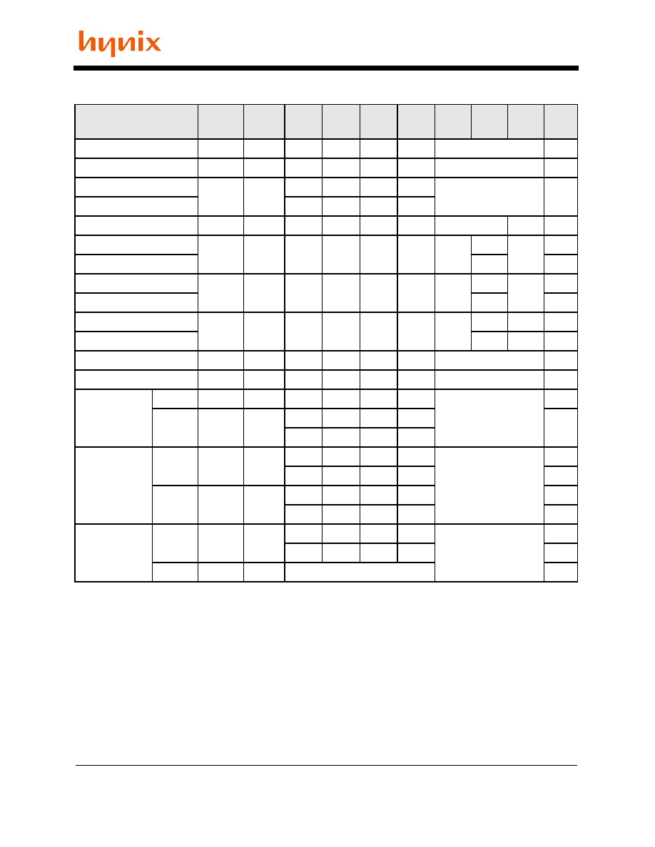
ORDERING INFORMATION
Part No.
Power Supply
Clock Frequency
Interface
Form Factor
HYMD232M646A(L)8-J
V
DD
=2.5V
V
DDQ
=2.5V
166MHz (*DDR333)
SSTL_2
200pin Unbuffered SO-DIMM
67.6mm x 31.75mm x 3.8mm
HYMD232M646A(L)8-M
133MHz (*DDR266:2-2-2)
HYMD232M646A(L)8-K
133MHz (*DDR266A)
HYMD232M646A(L)8-H
133MHz (*DDR266B)
HYMD232M646A(L)8-L
100MHz (*DDR200)
�
256MB (32M x 64) Unbuffered DDR SO-DIMM based
on 32Mx8 DDR SDRAM
�
JEDEC Standard 200-pin small outline dual in-line
memory module (SO-DIMM)
�
2.5V +/- 0.2V VDD and VDDQ Power supply
�
All inputs and outputs are compatible with SSTL_2
interface
�
Fully differential clock operations (CK & /CK) with
100MHz/125MHz/133MHz/166MHz
�
All addresses and control inputs except Data, Data
strobes and Data masks latched on the rising edges
of the clock
�
Data(DQ), Data strobes and Write masks latched on
both rising and falling edges of the clock
�
Data inputs on DQS centers when write (centered
DQ)
�
Data strobes synchronized with output data for read
and input data for write
�
Programmable CAS Latency 2 / 2.5 supported
�
Programmable Burst Length 2 / 4 / 8 with both
sequential and interleave mode
�
tRAS Lock-out function supported
�
Internal four bank operations with single pulsed RAS
�
Auto refresh and self refresh supported
�
8192 refresh cycles / 64ms
* JEDEC Defined Specifications compliant
HYMD232M646A(L)8-J/M/K/H/L
Rev. 0.2/May. 02
2
PIN DESCRIPTION
PIN ASSIGNMENT
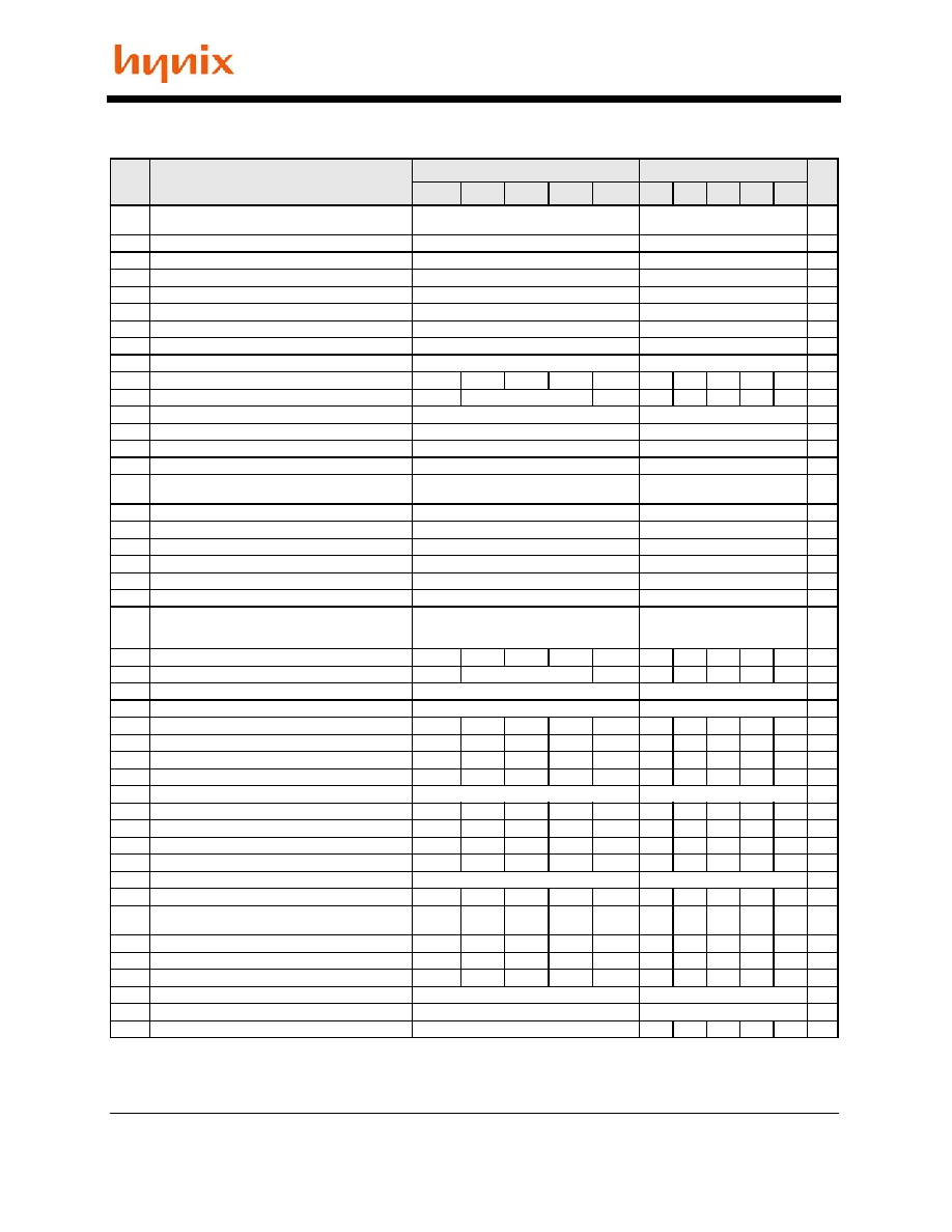
Pin
Pin Description
Pin
Pin Description
CK0, /CK0, CK1, /CK1
Differential Clock Inputs
VDDQ
DQs Power Supply
CS0, CS1
Chip Select Input
VSS
Ground
CKE0, CKE1
Clock Enable Input
VREF
Reference Power Supply
/RAS, /CAS, /WE
Commend Sets Inputs
VDDSPD
Power Supply for SPD
A0 ~ A12
Address
SA0~SA2
E
2
PROM Address Inputs
BA0, BA1
Bank Address
SCL
E
2
PROM Clock
DQ0~DQ63
Data Inputs/Outputs
SDA
E
2
PROM Data I/O
DQS0~DQS7
Data Strobe Inputs/Outputs
VDDID
VDD Identification Flag
DM0~DM7
Data-in Mask
DU
Do not Use
VDD
Power Supply
NC
No Connection
Pin
Name
Pin
Name
Pin
Name
Pin
Name
Pin
Name
Pin
Name
Pin
Name
Pin
Name
1
VREF
2
VREF
51
VSS
52
VSS
101
A9
102
A8
151
DQ42
152
DQ46
3
VSS
4
VSS
53
DQ19
54
DQ23
103
VSS
104
VSS
153
DQ43
154
DQ47
5
DQ0
6
DQ4
55
DQ24
56
DQ28
105
A7
106
A6
155
VDD
156
VDD
7
DQ1
8
DQ5
57
VDD
58
VDD
107
A5
108
A4
157
VDD
158
/CK1
9
VDD
10
VDD
59
DQ25
60
DQ29
109
A3
110
A2
159
VSS
160
CK1
11
DQS0
12
DM0
61
DQS3
62
DM3
111
A1
112
A0
161
VSS
162
VSS
13
DQ2
14
DQ6
63
VSS
64
VSS
113
VDD
114
VDD
163
DQ48
164
DQ52
15
VSS
16
VSS
65
DQ26
66
DQ30
115
A10/AP
116
BA1
165
DQ49
166
DQ53
17
DQ3
18
DQ7
67
DQ27
68
DQ31
117
BA0
118
/RAS
167
VDD
168
VDD
19
DQ8
20
DQ12
69
VDD
70
VDD
119
/WE
120
/CAS
169
DQS6
170
DM6
21
VDD
22
VDD
71
NC
72
NC
121
/CS0
122
/CS1
171
DQ50
172
DQ54
23
DQ9
24
DQ13
73
NC
74
NC
123
DU
124
DU
173
VSS
174
VSS
25
DQS1
26
DM1
75
VSS
76
VSS
125
VSS
126
VSS
175
DQ51
176
DQ55
27
VSS
28
VSS
77
NC
78
NC
127
DQ32
128
DQ36
177
DQ56
178
DQ60
29
DQ10
30
DQ14
79
NC
80
NC
129
DQ33
130
DQ37
179
VDD
180
VDD
31
DQ11
32
DQ15
81
VDD
82
VDD
131
VDD
132
VDD
181
DQ57
182
DQ61
33
VDD
34
VDD
83
NC
84
NC
133
DQS4
134
DM4
183
DQS7
184
DM7
35
CK0
36
VDD
85
DU
86
DU
135
DQ34
136
DQ38
185
VSS
186
VSS
37
/CK0
38
VSS
87
VSS
88
VSS
137
VSS
138
VSS
187
DQ58
188
DQ62
39
VSS
40
VSS
89
NC
90
VSS
139
DQ35
140
DQ39
189
DQ59
190
DQ63
41
DQ16
42
DQ20
91
NC
92
VDD
141
DQ40
142
DQ44
191
VDD
192
VDD
43
DQ17
44
DQ21
93
VDD
94
VDD
143
VDD
144
VDD
193
SDA
194
SA0
45
VDD
46
VDD
95
CKE1
96
CKE0
145
DQ41
146
DQ45
195
SCL
196
SA1
47
DQS2
48
DM2
97
NC
98
DU
147
DQS5
148
DM5
197 VDDSPD 198
SA2
49
DQ18
50
DQ22
99
A12
100
A11
149
VSS
150
VSS
199
VDDID
200
DU
HYMD232M646A(L)8-J/M/K/H/L
Rev. 0.2/May. 02
3
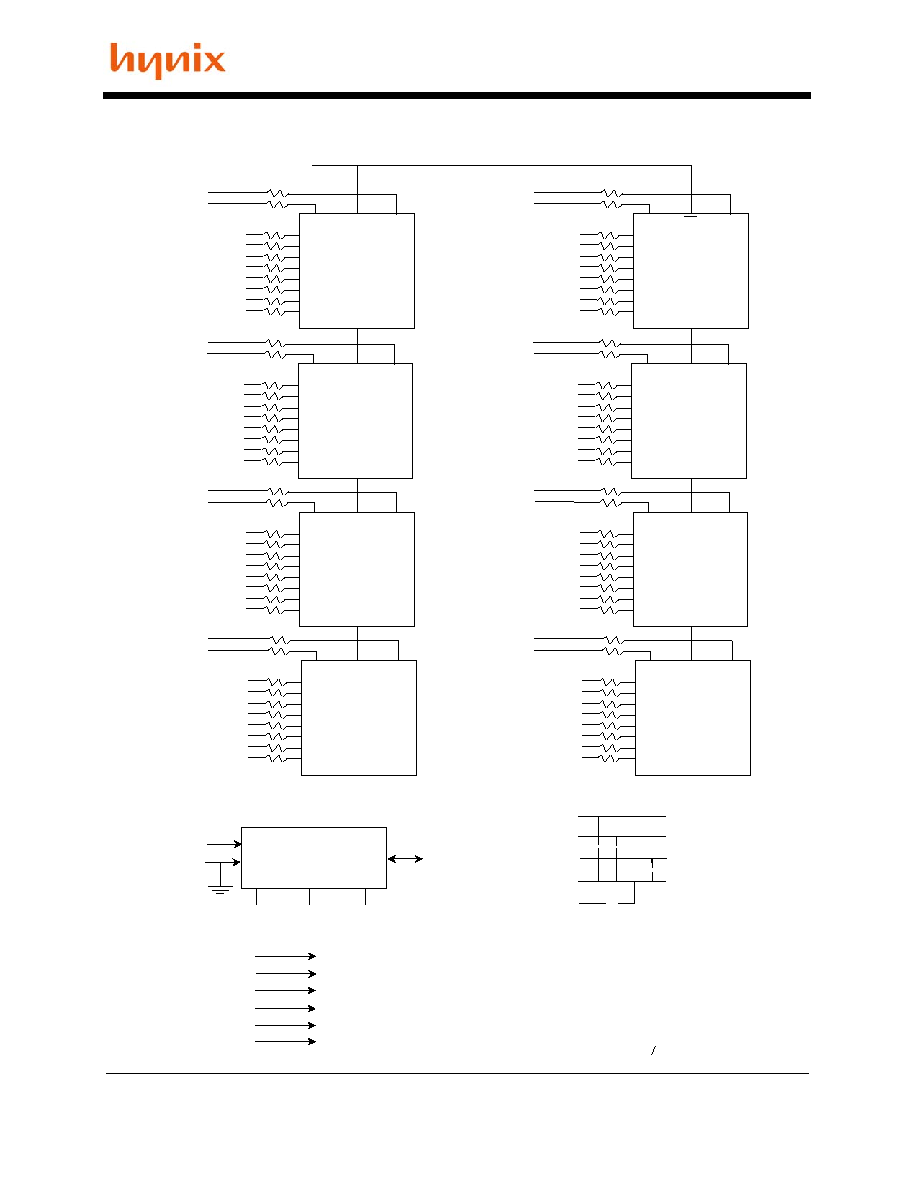
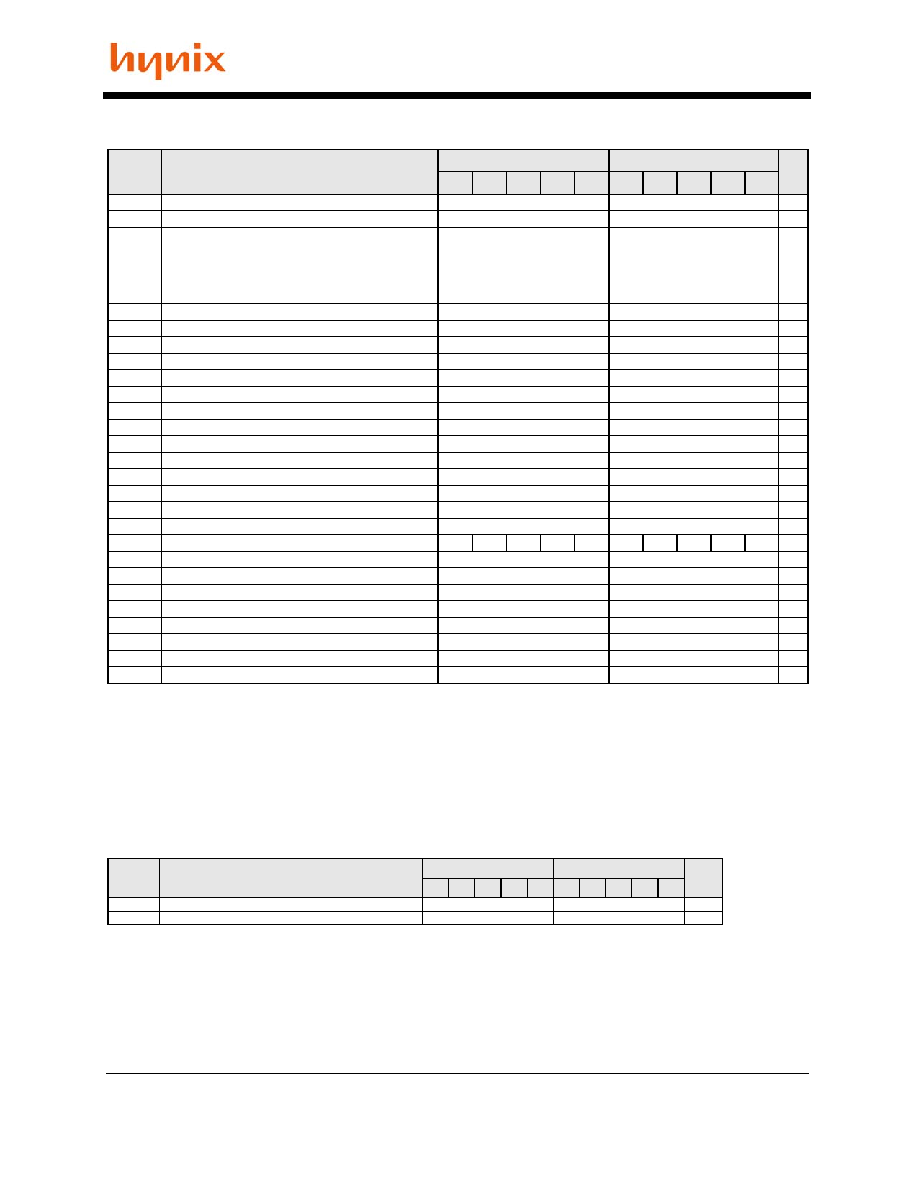
FUNCTIONAL BLOCK DIAGRAM
DQ0
DQ1
DQ2
DQ3
DQ4
DQ5
DQ6
DQ7
D0
/CS
DM
DM0
I/O 0
I/O 1
I/O 2
I/O 3
I/O 4
I/O 5
I/O 6
I/O 7
DQS
DQS0
DQ8
DQ9
DQ10
DQ11
DQ12
DQ13
DQ14
DQ15
D1
/CS
DM
DM1
I/O 0
I/O 1
I/O 2
I/O 3
I/O 4
I/O 5
I/O 6
I/O 7
DQS
DQS1
DQ16
DQ17
DQ18
DQ19
DQ20
DQ21
DQ22
DQ23
D2
/CS
DM
DM2
I/O 0
I/O 1
I/O 2
I/O 3
I/O 4
I/O 5
I/O 6
I/O 7
DQS
DQS2
DQ24
DQ25
DQ26
DQ27
DQ28
DQ29
DQ30
DQ31
D3
/CS
DM
DM3
I/O 0
I/O 1
I/O 2
I/O 3
I/O 4
I/O 5
I/O 6
I/O 7
DQS
DQS3
D4
CS
DM
DM4
I/O 0
I/O 1
I/O 2
I/O 3
I/O 4
I/O 5
I/O 6
I/O 7
DQS
DQ40
DQ41
DQ42
DQ43
DQ44
DQ45
DQ46
DQ47
D5
/CS
DM
DM5
I/O 0
I/O 1
I/O 2
I/O 3
I/O 4
I/O 5
I/O 6
I/O 7
DQS
DQS5
DQ48
DQ49
DQ50
DQ51
DQ52
DQ53
DQ54
DQ55
D6
/CS
DM
DM6
I/O 0
I/O 1
I/O 2
I/O 3
I/O 4
I/O 5
I/O 6
I/O 7
DQS
DQS6
DQ56
DQ57
DQ58
DQ59
DQ60
DQ61
DQ62
DQ63
D7
/CS
DM
DM7
I/O 0
I/O 1
I/O 2
I/O 3
I/O 4
I/O 5
I/O 6
I/O 7
DQS
DQS7
DQ32
DQ33
DQ34
DQ35
DQ36
DQ37
DQ38
DQ39
D4
DM
DQS
DQS4
/CS0
BA0-BA1 BA0-BA1 : SDRAMs D0 - D7
A0 - A12 A0 - A12 : SDRAMs D0 - D7
/RAS /RAS : SDRAMs D0 - D7
/CAS /CAS : SDRAMs D0 - D7
CKE0 CKE : SDRAMs D0 - D7
/WE /WE : SDRAMs D0 - D7
Notes:
1. DQ-to-I/O wiring is shown as recommended
but may be changed
2. DQ/DQS/DM/CKE/S relationships must be
maintained as shown
3. DQ, DQS, DM/DQS resistors : 22Ohms+/-5%
4. VDDID strap connections
(for memory device VDD, VDDQ) :
Strap out :(open) : VDD=VDDQ
Strap In (Vss) : VDD= VDDQ
. .
VDD/VDDQ
VDDSPD
VREF
VSS
VDDID
SPD
D0 - D7
D0 - D7
D0 - D7
=
.
=
.
=
.
.
.
. .
Strap:see Note 4
Serial PD
A0
A1
A2
SA0
SA1
SA2
SCL
WP
SDA
DQ0
DQ1
DQ2
DQ3
DQ4
DQ5
DQ6
DQ7
D0
/CS
DM
DM0
I/O 0
I/O 1
I/O 2
I/O 3
I/O 4
I/O 5
I/O 6
I/O 7
DQS
DQS0
DQ8
DQ9
DQ10
DQ11
DQ12
DQ13
DQ14
DQ15
D1
/CS
DM
DM1
I/O 0
I/O 1
I/O 2
I/O 3
I/O 4
I/O 5
I/O 6
I/O 7
DQS
DQS1
DQ16
DQ17
DQ18
DQ19
DQ20
DQ21
DQ22
DQ23
D2
/CS
DM
DM2
I/O 0
I/O 1
I/O 2
I/O 3
I/O 4
I/O 5
I/O 6
I/O 7
DQS
DQS2
DQ24
DQ25
DQ26
DQ27
DQ28
DQ29
DQ30
DQ31
D3
/CS
DM
DM3
I/O 0
I/O 1
I/O 2
I/O 3
I/O 4
I/O 5
I/O 6
I/O 7
DQS
DQS3
D4
CS
DM
DM4
I/O 0
I/O 1
I/O 2
I/O 3
I/O 4
I/O 5
I/O 6
I/O 7
DQS
DQ40
DQ41
DQ42
DQ43
DQ44
DQ45
DQ46
DQ47
D5
/CS
DM
DM5
I/O 0
I/O 1
I/O 2
I/O 3
I/O 4
I/O 5
I/O 6
I/O 7
DQS
DQS5
DQ48
DQ49
DQ50
DQ51
DQ52
DQ53
DQ54
DQ55
D6
/CS
DM
DM6
I/O 0
I/O 1
I/O 2
I/O 3
I/O 4
I/O 5
I/O 6
I/O 7
DQS
DQS6
DQ56
DQ57
DQ58
DQ59
DQ60
DQ61
DQ62
DQ63
D7
/CS
DM
DM7
I/O 0
I/O 1
I/O 2
I/O 3
I/O 4
I/O 5
I/O 6
I/O 7
DQS
DQS7
DQ32
DQ33
DQ34
DQ35
DQ36
DQ37
DQ38
DQ39
D4
DM
DQS
DQS4
/CS0
BA0-BA1 BA0-BA1 : SDRAMs D0 - D7
A0 - A12 A0 - A12 : SDRAMs D0 - D7
/RAS /RAS : SDRAMs D0 - D7
/CAS /CAS : SDRAMs D0 - D7
CKE0 CKE : SDRAMs D0 - D7
/WE /WE : SDRAMs D0 - D7
Notes:
1. DQ-to-I/O wiring is shown as recommended
but may be changed
2. DQ/DQS/DM/CKE/S relationships must be
maintained as shown
3. DQ, DQS, DM/DQS resistors : 22Ohms+/-5%
4. VDDID strap connections
(for memory device VDD, VDDQ) :
Strap out :(open) : VDD=VDDQ
Strap In (Vss) : VDD= VDDQ
. .
VDD/VDDQ
VDDSPD
VREF
VSS
VDDID
SPD
D0 - D7
D0 - D7
D0 - D7
=
.
=
.
=
.
.
.
. .
Strap:see Note 4
Serial PD
A0
A1
A2
SA0
SA1
SA2
SCL
WP
SDA
BA0-BA1 BA0-BA1 : SDRAMs D0 - D7
A0 - A12 A0 - A12 : SDRAMs D0 - D7
/RAS /RAS : SDRAMs D0 - D7
/CAS /CAS : SDRAMs D0 - D7
CKE0 CKE : SDRAMs D0 - D7
/WE /WE : SDRAMs D0 - D7
BA0-BA1 BA0-BA1 : SDRAMs D0 - D7
A0 - A12 A0 - A12 : SDRAMs D0 - D7
/RAS /RAS : SDRAMs D0 - D7
/CAS /CAS : SDRAMs D0 - D7
CKE0 CKE : SDRAMs D0 - D7
/WE /WE : SDRAMs D0 - D7
Notes:
1. DQ-to-I/O wiring is shown as recommended
but may be changed
2. DQ/DQS/DM/CKE/S relationships must be
maintained as shown
3. DQ, DQS, DM/DQS resistors : 22Ohms+/-5%
4. VDDID strap connections
(for memory device VDD, VDDQ) :
Strap out :(open) : VDD=VDDQ
Strap In (Vss) : VDD= VDDQ
Notes:
1. DQ-to-I/O wiring is shown as recommended
but may be changed
2. DQ/DQS/DM/CKE/S relationships must be
maintained as shown
3. DQ, DQS, DM/DQS resistors : 22Ohms+/-5%
4. VDDID strap connections
(for memory device VDD, VDDQ) :
Strap out :(open) : VDD=VDDQ
Strap In (Vss) : VDD= VDDQ
. .
VDD/VDDQ
VDDSPD
VREF
VSS
VDDID
SPD
D0 - D7
D0 - D7
D0 - D7
=
.
=
.
=
.
.
.
. .
Strap:see Note 4
. .
VDD/VDDQ
VDDSPD
VREF
VSS
VDDID
SPD
D0 - D7
D0 - D7
D0 - D7
=
.
=
.
=
.
.
.
. .
Strap:see Note 4
.
VDD/VDDQ
VDDSPD
VREF
VSS
VDDID
SPD
D0 - D7
D0 - D7
D0 - D7
=
.
=
.
=
.
.
.
. .
Strap:see Note 4
Serial PD
A0
A1
A2
SA0
SA1
SA2
SCL
WP
SDA
Serial PD
A0
A1
A2
SA0
SA1
SA2
SCL
WP
SDA
HYMD232M646A(L)8-J/M/K/H/L
Rev. 0.2/May. 02
4
ABSOLUTE MAXIMUM RATINGS
Note : Operation at above absolute maximum rating can adversely affect device reliability
DC OPERATING CONDITIONS
(TA= 0 to 70
o
C, Voltage referenced to V
SS
= 0V)
Note :
1. V
DDQ
must not exceed the level of V
DD
.
2. V
IL
(min) is acceptable -1.5V AC pulse width with < 5ns of duration.
3. The value of V
REF
is approximately equal to 0.5V
DDQ
.
AC OPERATING CONDITIONS
(TA= 0 to 70
o
C, Voltage referenced to V
SS
= 0V)
Note :
1. VID is the magnitude of the difference between the input level on CK and the input on /CK.
2. The value of V IX is expected to equal 0.5*V DDQ of the transmitting device and must track variations in the DC level of the same.
Parameter
Symbol
Rating
Unit
Ambient Temperature
T
A
0 ~ 70
o
C
Storage Temperature
T
STG
-55 ~ 125
o
C
Voltage on Any Pin relative to V
SS
V
IN
, V
OUT
-0.5 ~ 3.6
V
Voltage on V
DD
relative to V
SS
V
DD
-0.5 ~ 3.6
V
Voltage on V
DDQ
relative to V
SS
V
DDQ
-0.5 ~ 3.6
V
Output Short Circuit Current
I
OS
50
mA
Power Dissipation
P
D
8
W
Soldering Temperature
Time
T
SOLDER
260
/ 10
o
C
/ Sec
Parameter
Symbol
Min
Typ.
Max
Unit
Note
Power Supply Voltage
V
DD
2.3
2.5
2.7
V
Power Supply Voltage
V
DDQ
2.3
2.5
2.7
V
1
Input High Voltage
V
IH
V
REF
+ 0.15
-
V
DDQ
+ 0.3
V
Input Low Voltage
V
IL
-0.3
-
V
REF
- 0.15
V
2
Termination Voltage
V
TT
V
REF
- 0.04
V
REF
V
REF
+ 0.04
V
Reference Voltage
V
REF
1.15
1.25
1.35
V
3
Parameter
Symbol
Min
Max
Unit
Note
Input High (Logic 1) Voltage, DQ, DQS and DM signals
V
IH(AC)
V
REF
+ 0.31
V
Input Low (Logic 0) Voltage, DQ, DQS and DM signals
V
IL(AC)
V
REF
- 0.31
V
Input Differential Voltage, CK and /CK inputs
V
ID(AC)
0.7
V
DDQ
+ 0.6
V
1
Input Crossing Point Voltage, CK and /CK inputs
V
IX(AC)
0.5*V
DDQ
-0.2
0.5*V
DDQ
+0.2
V
2

HYMD232M646A(L)8-J/M/K/H/L
Rev. 0.2/May. 02
5
AC OPERATING TEST CONDITIONS
(TA=0 to 70
o
C, Voltage referenced to VSS = 0V)
Parameter
Value
Unit
Reference Voltage
V
DDQ
x 0.5
V
Termination Voltage
V
DDQ
x 0.5
V
AC Input High Level Voltage (V
IH
, min)
V
REF
+ 0.31
V
AC Input Low Level Voltage (V
IL
, max)
V
REF
- 0.31
V
Input Timing Measurement Reference Level Voltage
V
REF
V
Output Timing Measurement Reference Level Voltage
V
TT
V
Input Signal maximum peak swing
1.5
V
Input minimum Signal Slew Rate
1
V/ns
Termination Resistor (R
T
)
50
Series Resistor (R
S
)
25
Output Load Capacitance for Access Time Measurement (C
L
)
30
pF
HYMD232M646A(L)8-J/M/K/H/L
Rev. 0.2/May. 02
6
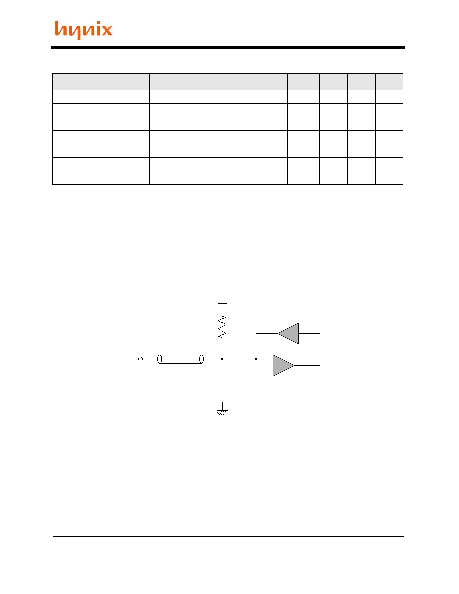
V
REF
V
TT
R
T
=50
Zo=50
C
L
=30pF
Output
CAPACITANCE
(T
A
=25
o
C, f=100MHz )
Note :
1. VDD = min. to max., VDDQ = 2.3V to 2.7V, VODC = VDDQ/2, V
O
peak-to-peak = 0.2V
2. Pins not under test are tied to GND.
3. These values are guaranteed by design and are tested on a sample basis only.
OUTPUT LOAD CIRCUIT
Parameter
Pin
Symbol
Min
Max
Unit
Input Capacitance
A0 ~ A12, BA0, BA1
C
IN1
TBD
TBD
pF
Input Capacitance
/RAS, /CAS, /WE
C
IN2
TBD
TBD
pF
Input Capacitance
CKE0, CKE1
C
IN3
TBD
TBD
pF
Input Capacitance
/CS0, /CS1
C
IN4
TBD
TBD
pF
Input Capacitance
CK0, /CK0, CK1, /CK1
C
IN5
TBD
TBD
pF
Input Capacitance
DM0 ~ DM7
C
IN6
TBD
TBD
pF
Data Input / Output Capacitance
DQ0 ~ DQ63, DQS0 ~ DQS7
C
IO1
TBD
TBD
pF
HYMD232M646A(L)8-J/M/K/H/L
Rev. 0.2/May. 02
7
DC CHARACTERISTICS I
(TA=0 to 70
o
C, Voltage referenced to V
SS
= 0V)
Note :
1. V
IN
= 0 to 3.6V, All other pins are not tested under V
IN
=0V
2. D
OUT
is disabled, V
OUT
=0 to 2.7V
Parameter
Symbol
Min.
Max
Unit
Note
Input Leakage
Current
Add, CMD, /CS, /CKE
I
LI
-16
16
uA
1
CK0, /CK0, CK1, /CK1
-8
8
CK2, /CK2
0
0
Output Leakage Current
I
LO
-5
5
uA
2
Output High Voltage
V
OH
V
TT
+ 0.76
-
V
I
OH
= -15.2mA
Output Low Voltage
V
OL
-
V
TT
- 0.76
V
I
OL
= +15.2mA
HYMD232M646A(L)8-J/M/K/H/L
Rev. 0.2/May. 02
8
DC CHARACTERISTICS II
(TA=0 to 70
o
C, Voltage referenced to V
SS
= 0V)
Parameter
Symbol
Test Condition
Speed
Unit Note
-J
-M
-K
-H
-L
Operating Current
IDD0
One bank; Active - Precharge;
tRC=tRC(min); tCK=tCK(min); DQ,DM and
DQS inputs changing twice per clock cycle
; address and control inputs changing once
per clock cycle
840
840
760
760
720
mA
Operating Current
IDD1
One bank; Active - Read - Precharge; Burst
Length=2; tRC=tRC(min); tCK=tCK(min);
address and control inputs changing once
per clock cycle
1200
1200
1040
1040
960
mA
Precharge Power
Down Standby Current
IDD2P
All banks idle; Power down - mode;
CKE=Low, tCK=tCK(min)
160
mA
Idle Standby Current
IDD2F
/CS=High, All banks idle; tCK=tCK(min);
CKE= High; address and control inputs
changing once per clock cycle. VIN=VREF
for DQ, DQS and DM
400
400
320
320
280
mA
Active Power Down
Standby Current
IDD3P
One bank active; Power down mode;
CKE=Low, tCK=tCK(min)
200
mA
Active Standby
Current
IDD3N
/CS=HIGH; CKE=HIGH; One bank; Active-
Precharge; tRC=tRAS(max);
tCK=tCK(min); DQ, DM and DQS inputs
changing twice per clock cycle; Address
and other control inputs changing once per
clock cycle
480
480
400
400
400
mA
Operating Current
IDD4R
Burst=2; Reads; Continuous burst; One
bank active; Address and control inputs
changing once per clock cycle;
tCK=tCK(min); IOUT=0mA
2320
2320
2000
2000
1520
mA
Operating Current
IDD4W
Burst=2; Writes; Continuous burst; One
bank active; Address and control inputs
changing once per clock cycle;
tCK=tCK(min); DQ, DM and DQS inputs
changing twice per clock cycle
2320
2320
2000
2000
1520
Auto Refresh Current
IDD5
tRC=tRFC(min) - 8*tCK for DDR200 at
100Mhz, 10*tCK for DDR266A & DDR266B
at 133Mhz; distributed refresh
1840
1840
1680
1680
1560
Self Refresh Current
IDD6
CKE=<0.2V; External clock
on; tCK =tCK(min)
Normal
24
mA
Low Power
12
mA
Operating Current -
Four Bank Operation
IDD7
Four bank interleaving with BL=4 Refer to
the following page for detailed test
condition
2520
2520
2440
2440
2240
mA
HYMD232M646A(L)8-J/M/K/H/L
Rev. 0.2/May. 02
9
AC CHARACTERISTICS
(AC operating conditions unless otherwise noted)
<DDR333, DDR266(2-2-2)>
Parameter
Symbol
DDR333
DDR266(2-2-2)
Unit
Note
Min
Max
Min
Max
Row Cycle Time
t
RC
60
-
60
-
ns
Auto Refresh Row Cycle Time
t
RFC
72
-
75
-
ns
Row Active Time
t
RAS
42
70K
45
120K
ns
Active to Read with Auto Precharge Delay
t
RAP
18
-
15
-
ns
16
Row Address to Column Address Delay
t
RCD
18
-
15
-
ns
Row Active to Row Active Delay
t
RRD
12
-
15
-
ns
Column Address to Column Address Delay
t
CCD
1
-
1
-
CK
Row Precharge Time
t
RP
18
-
15
-
ns
Write Recovery Time
tWR
15
-
15
-
ns
Write to Read Command Delay
t
WTR
1
-
1
-
CK
Auto Precharge Write Recovery + Precharge Time
t
DAL
(tWR/tCK)
+
(tRP/tCK)
-
(tWR/tCK)
+
(tRP/tCK)
-
CK
15
System Clock Cycle Time
CL = 2.5
t
CK
6
12
7.5
12
ns
CL = 2
7.5
12
7.5
12
ns
Clock High Level Width
t
CH
0.45
0.55
0.45
0.55
CK
Clock Low Level Width
t
CL
0.45
0.55
0.45
0.55
CK
Data-Out edge to Clock edge Skew
t
AC
-0.7
0.7
-0.75
0.75
ns
DQS-Out edge to Clock edge Skew
t
DQSCK
-0.6
0.6
-0.75
0.75
ns
DQS-Out edge to Data-Out edge Skew
t
DQSQ
-
0.45
-
0.5
ns
Data-Out hold time from DQS
t
QH
t
HP
-t
QHS
-
t
HP
-t
QHS
-
ns
1, 10
Clock Half Period
t
HP
min
(tCL,tCH)
-
min
(tCL,tCH)
-
ns
1,9
Data Hold Skew Factor
t
QHS
-
0.55
-
0.75
ns
10
Valid Data Output Window
t
DV
t
QH
-t
DQSQ
t
QH
-t
DQSQ
ns
Data-out high-impedance window from CK, /CK
t
HZ
-0.7
0.7
-0.75
0.75
ns
17
Data-out low-impedance window from CK, /CK
t
LZ
-0.7
0.7
-0.75
0.75
ns
17
Input Setup Time (fast slew rate)
t
IS
0.75
-
0.9
-
ns
2,3,5,6
Input Hold Time (fast slew rate)
t
IH
0.75
-
0.9
-
ns
2,3,5,6
Input Setup Time (slow slew rate)
t
IS
0.8
-
1.0
-
ns
2,4,5,6
Input Hold Time (slow slew rate)
t
IH
0.8
-
1.0
-
ns
2,4,5,6
Input Pulse Width
t
IPW
2.2
2.2
ns
6
Write DQS High Level Width
t
DQSH
0.35
-
0.35
-
CK
HYMD232M646A(L)8-J/M/K/H/L
Rev. 0.2/May. 02
10
AC CHARACTERISTICS
(AC operating conditions unless otherwise noted)
- continued -
Parameter
Symbol
DDR333
DDR266(2-2-2)
Unit
Note
Min
Max
Min
Max
Write DQS Low Level Width
t
DQSL
0.35
-
0.35
-
CK
Clock to First Rising edge of DQS-In
t
DQSS
0.75
1.25
0.72
1.28
CK
Data-In Setup Time to DQS-In (DQ & DM)
t
DS
0.45
-
0.5
-
ns
6,7, 11~13
Data-in Hold Time to DQS-In (DQ & DM)
t
DH
0.45
-
0.5
-
ns
6,7, 11~13
DQ & DM Input Pulse Width
t
DIPW
1.75
-
1.75
-
ns
Read DQS Preamble Time
t
RPRE
0.9
1.1
0.9
1.1
CK
Read DQS Postamble Time
t
RPST
0.4
0.6
0.4
0.6
CK
Write DQS Preamble Setup Time
t
WPRES
0
-
0
-
CK
Write DQS Preamble Hold Time
t
WPREH
0.25
-
0.25
-
CK
Write DQS Postamble Time
t
WPST
0.4
0.6
0.4
0.6
CK
Mode Register Set Delay
t
MRD
2
-
2
-
CK
Exit Self Refresh to Any Execute Command
t
XSC
200
-
200
-
CK
8
Average Periodic Refresh Interval
t
REFI
-
15.6
-
15.6
us
HYMD232M646A(L)8-J/M/K/H/L
Rev. 0.2/May. 02
11
AC CHARACTERISTICS
(AC operating conditions unless otherwise noted)
<DDR266A/B, DDR200>
Parameter
Symbol
DDR266A
DDR266B
DDR200
Unit
Note
Min
Max
Min
Max
Min
Max
Row Cycle Time
t
RC
65
-
65
-
70
-
ns
Auto Refresh Row Cycle Time
t
RFC
75
-
75
-
80
-
ns
Row Active Time
t
RAS
45
120K
45
120K
50
120k
ns
Active to Read with Auto Precharge Delay
t
RAP
20
-
20
-
20
-
ns
16
Row Address to Column Address Delay
t
RCD
20
-
20
-
20
-
ns
Row Active to Row Active Delay
t
RRD
15
-
15
-
15
-
ns
Column Address to Column Address Delay
t
CCD
1
-
1
-
1
-
CK
Row Precharge Time
t
RP
20
-
20
-
20
-
ns
Write Recovery Time
tWR
15
-
15
-
15
-
ns
Write to Read Command Delay
t
WTR
1
-
1
-
1
-
CK
Auto Precharge Write Recovery + Precharge
Time
t
DAL
(tWR/tCK)
+
(tRP/tCK)
-
(tWR/tCK)
+
(tRP/tCK)
-
(tWR/tCK)
+
(tRP/tCK)
-
CK
15
System Clock Cycle Time
CL = 2.5
t
CK
7.5
12
7.5
12
8.0
12
ns
CL = 2
7.5
12
10
12
10
12
ns
Clock High Level Width
t
CH
0.45
0.55
0.45
0.55
0.45
0.55
CK
Clock Low Level Width
t
CL
0.45
0.55
0.45
0.55
0.45
0.55
CK
Data-Out edge to Clock edge Skew
t
AC
-0.75
0.75
-0.75
0.75
-0.8
0.8
ns
DQS-Out edge to Clock edge Skew
t
DQSCK
-0.75
0.75
-0.75
0.75
-0.8
0.8
ns
DQS-Out edge to Data-Out edge Skew
t
DQSQ
-
0.5
-
0.5
-
0.6
ns
Data-Out hold time from DQS
t
QH
t
HP
-t
QHS
-
t
HP
-t
QHS
-
t
HP
-t
QHS
-
ns
1, 10
Clock Half Period
t
HP
min
(tCL,tCH)
-
min
(tCL,tCH)
-
min
(tCL,tCH)
-
ns
1,9
Data Hold Skew Factor
t
QHS
-
0.75
-
0.75
-
0.75
ns
10
Valid Data Output Window
t
DV
t
QH
-t
DQSQ
t
QH
-t
DQSQ
t
QH
-t
DQSQ
ns
Data-out high-impedance window from CK, /CK
t
HZ
-0.75
0.75
-0.75
0.75
-0.8
0.8
ns
17
Data-out low-impedance window from CK, /CK
t
LZ
-0.75
0.75
-0.75
0.75
-0.8
0.8
ns
17
Input Setup Time (fast slew rate)
t
IS
0.9
-
0.9
-
1.1
-
ns
2,3,5,6
Input Hold Time (fast slew rate)
t
IH
0.9
-
0.9
-
1.1
-
ns
2,3,5,6
Input Setup Time (slow slew rate)
t
IS
1.0
-
1.0
-
1.1
-
ns
2,4,5,6
Input Hold Time (slow slew rate)
t
IH
1.0
-
1.0
-
1.1
-
ns
2,4,5,6
Input Pulse Width
t
IPW
2.2
2.2
2.5
-
ns
6
Write DQS High Level Width
t
DQSH
0.35
-
0.35
-
0.35
-
CK
HYMD232M646A(L)8-J/M/K/H/L
Rev. 0.2/May. 02
12
- continued -
Parameter
Symbol
DDR266A
DDR266B
DDR200
Unit
Note
Min
Max
Min
Max
Min
Max
Write DQS Low Level Width
t
DQSL
0.35
-
0.35
-
0.35
-
CK
Clock to First Rising edge of DQS-In
t
DQSS
0.75
1.25
0.75
1.25
0.72
1.28
CK
Data-In Setup Time to DQS-In (DQ & DM)
t
DS
0.45
-
0.45
-
0.5
-
ns
6,7,
11~13
Data-in Hold Time to DQS-In (DQ & DM)
t
DH
0.45
-
0.45
-
0.5
-
ns
DQ & DM Input Pulse Width
t
DIPW
1.75
-
1.75
-
1.75
-
ns
Read DQS Preamble Time
t
RPRE
0.9
1.1
0.9
1.1
0.9
1.1
CK
Read DQS Postamble Time
t
RPST
0.4
0.6
0.4
0.6
0.4
0.6
CK
Write DQS Preamble Setup Time
t
WPRES
0
-
0
-
0
-
CK
Write DQS Preamble Hold Time
t
WPREH
0.25
-
0.25
-
0.25
-
CK
Write DQS Postamble Time
t
WPST
0.4
0.6
0.4
0.6
0.4
0.6
CK
Mode Register Set Delay
t
MRD
2
-
2
-
2
-
CK
Exit Self Refresh to Any Execute Command
t
XSC
200
-
200
-
200
-
CK
8
Average Periodic Refresh Interval
t
REFI
-
15.6
-
15.6
-
15.6
us
HYMD232M646A(L)8-J/M/K/H/L
Rev. 0.2/May. 02
13
Note :
1.
This calculation accounts for tDQSQ(max), the pulse width distortion of on-chip circuit and jitter.
2.
Data sampled at the rising edges of the clock : A0~A12, BA0~BA1, CKE, /CS, /RAS, /CAS, /WE.
3.
For command/address input slew rate >=1.0V/ns
4.
For command/address input slew rate >=0.5V/ns and <1.0V/ns
This derating table is used to increase tIS/tIH in case where the input slew-rate is below 0.5V/ns.
Input Setup / Hold Slew-rate Derating Table.
5. CK, /CK slew rates are >=1.0V/ns
6. These parameters quarantee device timing, but they are not necessarily tested on each device, and they may be quaranteed by
design or tester correlation.
7. Data latched at both rising and falling edges of Data Strobes(LDQS/UDQS) : DQ, LDM/UDM.
8. Minimum of 200 cycles of stable input clocks after Self Refresh Exit command, where CKE is held high, is required to complete
Self Refresh Exit and lock the internal DLL circuit of DDR SDRAM.
9. Min (tCL, tCH) refers to the smaller of the actual clock low time and the actual clock high time as provided to the device
(i.e. this value can be greater than the minimum specification limits for tCL and tCH).
10. tHP = minimum half clock period for any given cycle and is defined by clock high or clock low (tCH, tCL). tQHS consists of
tDQSQmax, the pulse width distortion of on-chip clock circuits, data pin to pin skew and output pattern effects and p-channel
to n-channel variation of the output drivers.
11
.
This derating table is used to increase tDS/tDH in case where the input slew-rate is below 0.5V/ns.
Input Setup / Hold Slew-rate Derating Table.
12. I/O Setup/Hold Plateau Derating. This derating table is used to increase tDS/tDH in case where the input level is flat below
VREF +/-310mV for a duration of up to 2ns.
13. I/O Setup/Hold Delta Inverse Slew Rate Derating. This derating table is used to increase tDS/tDH in case where the DQ and
DQS slew rates differ. The Delta Inverse Slew Rate is calculated as (1/SlewRate1)-(1/SlewRate2). For example, if slew rate
1=0.5V/ns and Slew Rate2 = 0.4V/n then the Delta Inverse Slew Rate = -0.5ns/V.
Input Setup / Hold Slew-rate
Delta tIS
Delta tIH
V/ns
ps
ps
0.5
0
0
0.4
+50
0
0.3
+100
0
Input Setup / Hold Slew-rate
Delta tDS
Delta tDH
V/ns
ps
ps
0.5
0
0
0.4
+75
+75
0.3
+150
+150
I/O Input Level
Delta tDS
Delta tDH
mV
ps
ps
+280
+50
+50
(1/SlewRate1)-(1/SlewRate2)
Delta tDS
Delta tDH
ns/V
ps
ps
0
0
0
+/-0.25
+50
+50
+/- 0.5
+100
+100

HYMD232M646A(L)8-J/M/K/H/L
Rev. 0.2/May. 02
14
14. DQS, DM and DQ input slew rate is specified to prevent double clocking of data and preserve setup and hold times.
Signal transi tions through the DC region must be monotonic.
15. tDAL = (tDPL / tCK ) + (tRP / tCK ). For each of the terms above, if not already an integer, round to the next highest integer.
tCK is equal to the actual system clock cycle time.
Example: For DDR266B at CL=2.5 and tCK = 7.5 ns,
tDAL = (15 ns / 7.5 ns) + (20 ns / 7.5 ns) = (2.00) + (2.67)
Round up each non-integer to the next highest integer: = (2) + (3), tDAL = 5 clock
16. For the parts which do not has internal RAS lockout circuit, Active to Read with Auto precharge delay should be
tRAS - BL/2 x tCK.
17. tHZ and tLZ transitions occur in the same access time windows as valid data trasitions. These parameters are not referenced
to a specific voltage level but specify when the device output is no longer driving (HZ), or begins driving (LZ).
HYMD232M646A(L)8-J/M/K/H/L
Rev. 0.2/May. 02
15
SIMPLIFIED COMMAND TRUTH TABLE
Note :
1. LDM/UDM states are Don't Care. Refer to below Write Mask Truth Table.
2. OP Code(Operand Code) consists of A
0
~A
12
and BA
0
~BA
1
used for Mode Registering duing Extended MRS or MRS.
Before entering Mode Register Set mode, all banks must be in a precharge state and MRS command can be issued after tRP
period from Prechagre command.
3. If a Read with Autoprecharge command is detected by memory component in CK(n), then there will be no command presented
to activated bank until CK(n+BL/2+t
RP
).
4. If a Write with Autoprecharge command is detected by memory compoment in CK(n), then there will be no command presented
to activated bank until CK(n+BL/2+1+t
DPL
+t
RP
). Last Data-In to Prechage delay(t
DPL
) which is also called Write Recovery Time
(tWR) is needed to guarantee that the last data has been completely written.
5. If A
10
/AP is High when Row Precharge command being issued, BA
0
/BA
1
are ignored and all banks are selected to be
precharged.
Command
CKEn-1
CKEn
/CS
/RAS
/CAS
/WE
ADDR
A10/
AP
BA
Note
Extended Mode Register Set
H
X
L
L
L
L
OP code
1,2
Mode Register Set
H
X
L
L
L
L
OP code
1,2
Device Deselect
H
X
H
X
X
X
X
1
No Operation
L
H
H
H
Bank Active
H
X
L
L
H
H
RA
V
1
Read
H
X
L
H
L
H
CA
L
V
1
Read with Autoprecharge
H
1,3
Write
H
X
L
H
L
L
CA
L
V
1
Write with Autoprecharge
H
1,4
Precharge All Banks
H
X
L
L
H
L
X
H
X
1,5
Precharge selected Bank
L
V
1
Read Burst Stop
H
X
L
H
H
L
X
1
Auto Refresh
H
H
L
L
L
H
X
1
Self Refresh
Entry
H
L
L
L
L
H
X
1
Exit
L
H
H
X
X
X
1
L
H
H
H
Precharge
Power Down
Mode
Entry
H
L
H
X
X
X
X
1
L
H
H
H
1
Exit
L
H
H
X
X
X
1
L
H
H
H
1
Active Power
Down Mode
(Clock Suspend)
Entry
H
L
H
X
X
X
X
1
L
V
V
V
1
Exit
L
H
X
1
( H=Logic High Level, L=Logic Low Level, X=Don't Care, V=Valid Data Input, OP Code=Operand Code, NOP=No Operation )

HYMD232M646A(L)8-J/M/K/H/L
Rev. 0.2/May. 02
16
MODULE DIMENSIONS
Front
31.75 mm
20.00 mm
1
39
41
199
1
39
41
199
Back
2.0 mm
2.0 mm
Side
(Front)
3.8mm
MAX.
67.60 mm

SERIAL PRESENCE DETECT
Rev. 0.2/May. 02
17
SPD SPECIFICATION
(32Mx64 Unbuffered DDR SO-DIMM)
HYMD232M646A(L)8-J/M/K/H/L
Rev. 0.2/May. 02
18
SERIAL PRESENCE DETECT
Byte#
Function Description
Function Supported
Hexa Value
Note
J
M
K
H
L
J
M
K
H
L
0
Number of Bytes written into serial memory at module
manufacturer
128 Bytes
80h
1
Total number of Bytes in SPD device
256 Bytes
08h
2
Fundamental memory type
DDR SDRAM
07h
3
Number of row address on this assembly
13
0Dh
1
4
Number of column address on this assembly
10
0Ah
1
5
Number of physical banks on DIMM
1Bank
01h
6
Module data width
64 Bits
40h
7
Module data width (continued)
-
00h
8
Module voltage Interface levels(VDDQ)
SSTL 2.5V
04h
9
DDR SDRAM cycle time at CAS Latency=2.5(tCK)
6.0ns
7.5ns
7.5ns
7.5ns
8.0ns
60h
75h
75h
75h
80h
2
10
DDR SDRAM access time from clock at CL=2.5 (tAC) +/-0.7ns
+/-0.75ns
+/-0.8ns 70h
75h
75h
75h
80h
2
11
Module configuration type
Non-ECC
00h
12
Refresh rate and type
7.8us & Self refresh
82h
13
Primary DDR SDRAM width
x8
08h
14
Error checking DDR SDRAM data width
N/A
00h
15
Minimum clock delay for back-to-back random col-
umn address(tCCD)
1 CLK
01h
16
Burst lengths supported
2,4,8
0Eh
17
Number of banks on each DDR SDRAM
4 Banks
04h
18
CAS latency supported
2, 2.5
0Ch
19
CS latency
0
01h
20
WE latency
1
02h
21
DDR SDRAM module attributes
Differential Clock Input
20h
22
DDR SDRAM device attributes : General
+/-0.2Voltage tolerance,
Concurrent Auto Precharge
tRAS Lock Out
C0h
23
DDR SDRAM cycle time at CL=2.0(tCK)
7.5ns
7.5ns
7.5ns
10ns
10ns
75h
75h
75h
A0h
A0h
2
24
DDR SDRAM access time from clock at CL=2.0(tAC) +/-0.7ns
+/-0.75ns
+/-0.8ns 70h
75h
75h
75h
80h
2
25
DDR SDRAM cycle time at CL=1.5(tCK)
-
00h
2
26
DDR SDRAM access time from clock at CL=1.5(tAC)
-
00h
2
27
Minimum row precharge time(tRP)
18ns
15ns
20ns
20ns
20ns
48h
3Ch
50h
50h
50h
28
Minimum row activate to row active delay(tRRD)
12ns
15ns
15ns
15ns
15ns
30h
3Ch
3Ch
3Ch
3Ch
29
Minimum RAS to CAS delay(tRCD)
18ns
15ns
20ns
20ns
20ns
48h
3Ch
50h
50h
50h
30
Minimum active to precharge time(tRAS)
42ns
45ns
45ns
45ns
50ns
2Ah
2Dh
2Dh
2Dh
32h
31
Module row density
256MB
40h
32
Command and address signal input setup time(tIS)
0.75ns
0.9ns
0.9ns
0.9ns
1.1ns
75h
90h
90h
90h
B0h
33
Command and address signal input hold time(tIH)
0.75ns
0.9ns
0.9ns
0.9ns
1.1ns
75h
90h
90h
90h
B0h
34
Data signal input setup time(tDS)
0.45ns
0.5ns
0.5ns
0.5ns
0.6ns
45h
50h
50h
50h
60h
35
Data signal input hold time(tDH)
0.45ns
0.5ns
0.5ns
0.5ns
0.6ns
45h
50h
50h
50h
60h
36~40 Reserved for VCSDRAM
Undefined
00h
41
Minimum active / auto-refresh time ( tRC)
60ns
60ns
65ns
65ns
70ns
3Ch
3Ch
41h
41h
46h
42
Minimum auto-refresh to active/auto-refresh
command period(tRFC)
72ns
75ns
75ns
75ns
80ns
48h
4Bh
4Bh
4Bh
50h
43
Maximum cycle time (tCK max)
12ns
12ns
12ns
12ns
12ns
30h
30h
30h
30h
30h
44
Maximim DQS-DQ skew time(tDQSQ)
0.45ns
0.5ns
0.5ns
0.5ns
0.6ns
2Dh
32h
32h
32h
3Ch
45
Maximum read data hold skew factor(tQHS)
0.55ns
0.75ns 0.75ns 0.75ns
0.75ns
55h
75h
75h
75h
75h
46~61 Superset information(may be used in future)
Undefined
00h
62
SPD Revision code
Initial release
00h
63
Checksum for Bytes 0~62
-
00h
BAh
B7h
E2h
7Ch
Bin Sort :J(DDR333),M(DDR266(2-2-2)),K(DDR266A@CL=2)
H(DDR266B@CL=2.5),L(DDR200@CL=2)
HYMD232M646A(L)8-J/M/K/H/L
Rev. 0.2/May. 02
19
SERIAL PRESENCE DETECT
- continued -
Note :
1. The bank address is excluded
2. These value is based on the component specification
3. These bytes are programmed by code of date week & date year
4. These bytes apply to Hynix's own Module Serial Number system
5. These bytes undefined and coded as `00h'
6. Refer to Hynix web site
Byte 85~86, Low power part
Byte #
Function Description
Function Supported
Hexa Value
Not
e
J
M
K
H
L
J
M
K
H
L
64
Manufacturer JEDEC ID Code
Hynix JEDEC ID
ADh
65~71
--------- Manufacturer JEDEC ID Code
-
00h
72
Manufacturing location
Hynix(Korea Area)
HSA(United States Area)
HSE(Europe Area)
HSJ(Japan Area)
Singapore
Asia Area
0*h
1*h
2*h
3*h
4*h
5*h
6
73
Manufacture part number(Hynix Memory Module)
H
48h
74
-------- Manufacture part number(Hynix Memory Module)
Y
59h
75
-------- Manufacture part number(Hynix Memory Module)
M
4Dh
76
Manufacture part number (DDR SDRAM)
D
44h
77
Manufacture part number(Memory density)
2
32h
78
Manufacture part number(Module Depth)
3
33h
79
------- Manufacture part number(Module Depth)
2
32h
80
Manufacture part number(Module type)
M
4Dh
81
Manufacture part number(Data width)
6
36h
82
-------Manufacture part number(Data width)
4
34h
83
Manufacture part number(Refresh, # of Bank.)
6(8K refresh,4Bank)
36h
84
Manufacture part number(Component Generation)
A
41h
85
Manufacture part number(Component configuration)
8
38h
86
Manufacture part number(Hyphen)
`-'
2Dh
87
Manufacture part number(Minimum cycle time)
J
M
K
H
L
4Ah
4Dh
4Bh
48h
4Ch
88~90
Manufacture part number(T.B.D)
Blank
20h
91
Manufacture revision code(for Component)
Blank
20h
92
Manufacture revision code (for PCB)
0
30h
93
Manufacturing date(Year)
-
-
3
94
Manufacturing date(Week)
-
-
3
95~98
Module serial number
-
-
4
99~127
Manufacturer specific data (may be used in future)
Undefined
00h
5
128~255 Open for customer use
Undefined
00h
5
Byte #
Function Description
Function Supported
Hexa Value
Note
J
M
K
H
L
J
M
K
H
L
85
Manufacture part number(Low power part)
L
4Ch
86
Manufacture part number(Component configuration)
8
38h