This document is a general product description and is subject to change without notice. Hynix Semiconductor does not assume any
responsibility for use of circuits described. No patent licenses are implied.
Rev. 1.0 / Feb. 2005 1
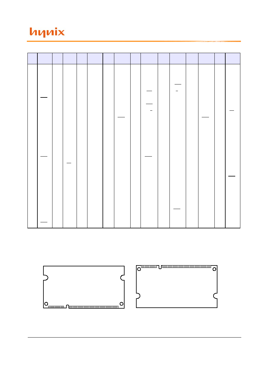
200pin Unbuffered DDR2 SDRAM SO-DIMMs based on 512 Mb 1st ver.
This Hynix unbuffered Slim Outline Dual In-Line Memory Module(DIMM) series consists of 512Mb 1st ver. DDR2
SDRAMs in Fine Ball Grid Array(FBGA) packages on a 200pin glass-epoxy substrate. This Hynix 512Mb 1st ver. based
Unbuffered DDR2 SO-DIMM series provide a high performance 8 byte interface in 67.60mm width form factor of indus-
try standard. It is suitable for easy interchange and addition.
FEATURES
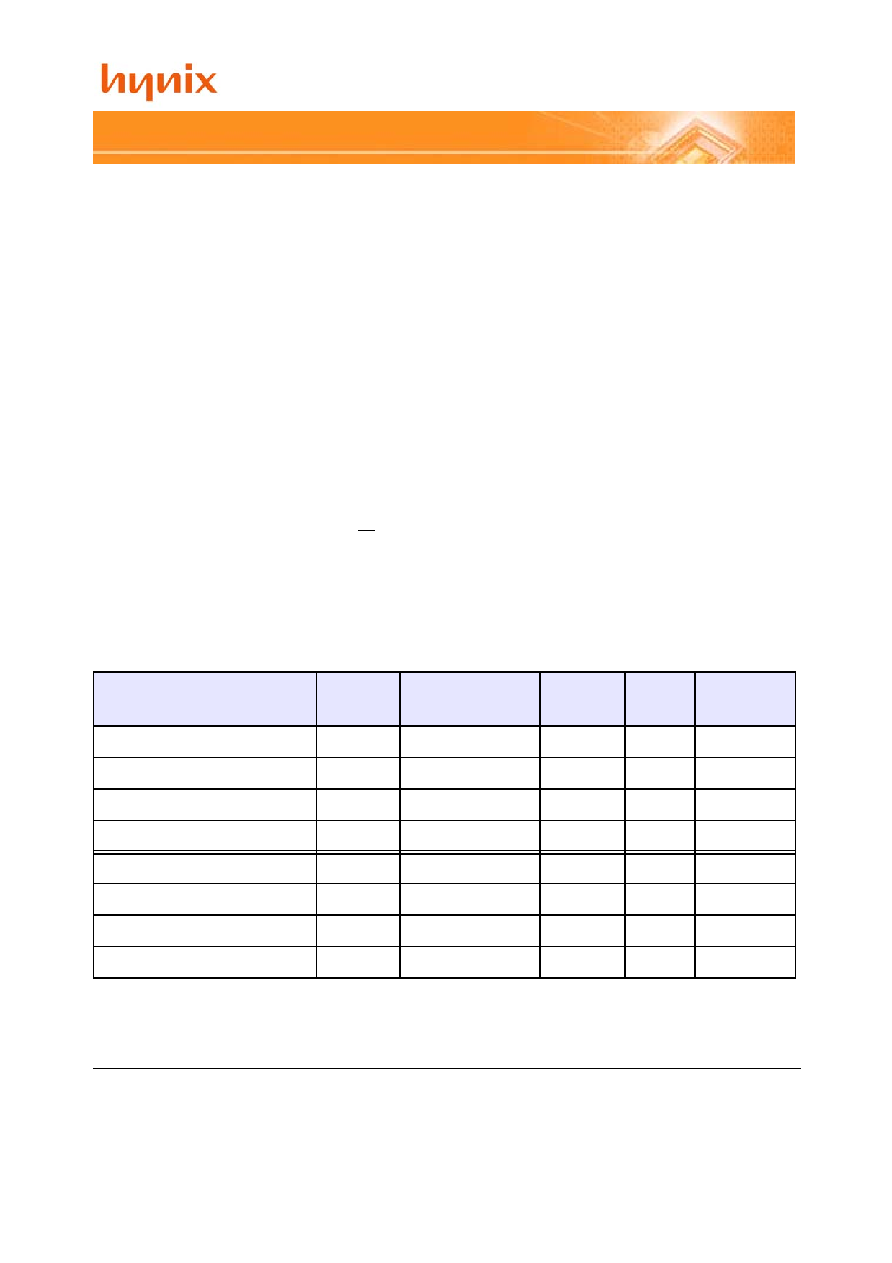
ORDERING INFORMATION
Part Name
Density
Organization
# of
DRAMs
# of
ranks
Materials
HYMP532S646-E3/C4
256MB
32Mx64
4
1
Leaded
HYMP564S648-E3/C4
512MB
64Mx64
8
1
Leaded
HYMP564S646-E3/C4
512MB
64Mx64
8
2
Leaded
HYMP112S64M8-E3/C4
1GB
128Mx64
16
2
Leaded
HYMP532S64P6-E3/C4
256MB
32Mx64
4
1
Lead free
HYMP564S64P8-E3/C4
512MB
64Mx64
8
1
Lead free
HYMP564S64P6-E3/C4
512MB
64Mx64
8
2
Lead free
HYMP112S64MP8-E3/C4
1GB
128Mx64
16
2
Lead free
�
JEDEC standard Double Data Rate2 Synchronous
DRAMs (DDR2 SDRAMs) with 1.8V +/- 0.1V Power
Supply
�
All inputs and outputs are compatible with SSTL_1.8
interface
�
Posted CAS
�
Programmable CAS Latency 3 ,4 ,5
�
OCD (Off-Chip Driver Impedance Adjustment) and
ODT (On-Die Termination)
�
Fully differential clock operations (CK & CK)
�
Programmable Burst Length 4 / 8 with both sequen-
tial and interleave mode
�
Auto refresh and self refresh supported
�
8192 refresh cycles / 64ms
�
Serial presence detect with EEPROM
�
DDR2 SDRAM Package: 60ball(x8), 84ball(x16)
FBGA
�
67.60 x 30.00 mm form factor
�
Lead-free Products are RoHS compliant
Rev. 1.0 / Feb. 2005
2
1
200pin Unbuffered DDR2 SDRAM SO-DIMMs
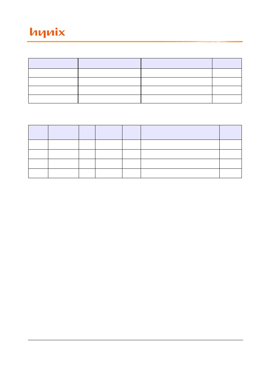
SPEED GRADE & KEY PARAMETERS
ADDRESS TABLE
E3 (DDR2-400)
C4 (DDR2-533)
Unit
Speed@CL3
400
400
Mbps
Speed@CL4
400
533
Mbps
Speed@CL5
-
-
Mbps
CL-tRCD-tRP
3-3-3
4-4-4
tCK
Density Organization Ranks
SDRAMs
# of
DRAMs
# of row/bank/column Address
Refresh
Method
256MB
32M x 64
1
32Mb x 16
4
13(A0~A12)/2(BA0~BA1)/10(A0~A9)
8K / 64ms
512MB
64M x 64
2
64Mb x 8
8
14(A0~A13)/2(BA0~BA1)/10(A0~A9)
8K / 64ms
512MB
64M x 64
1
32Mb x 16
8
13(A0~A12)/2(BA0~BA1)/10(A0~A9)
8K / 64ms
1GB
128M x 64
2
64Mb x 8
16
14(A0~A13)/2(BA0~BA1)/10(A0~A9)
8K / 64ms
Rev. 1.0 / Feb. 2005
3
1
200pin Unbuffered DDR2 SDRAM SO-DIMMs
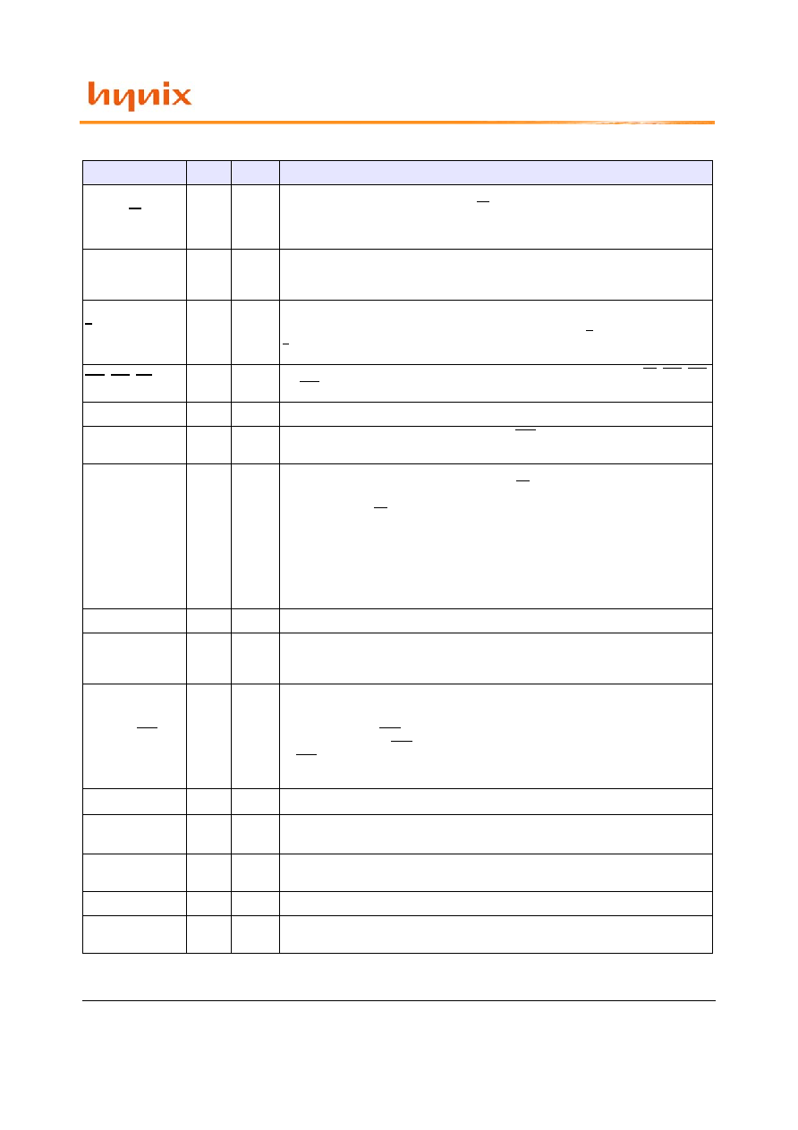
PIN DESCRIPTION
Symbol
Type
Polarity
Pin Description
CK[1:0], CK[1:0]
Input
Cross
Point
The system clock inputs. All adress an commands lines are sampled on the cross point of
the rising edge of CK and falling edge of CK. A Delay Locked Loop(DLL) circuit is driven
from the clock inputs and output timing for read operations is synchronized to the input
clock.
CKE[1:0]
Input
Active
High
Activates the DDR2 SDRAM CK signal when high and deactivates the CK signal when low.
By deactivating the clocks, CKE low initiates the Power Down mode or the Self Refresh
mode.
S[1:0]
Input
Active
Low
Enables the associated DDR2 SDRAM command decoder when low and disables the com-
mand decoder when high. When the command decoder is disabled, new commands are
ignored but previous operations continue. Rank 0 is selected by S0; Rank 1 is selected by
S1
RAS, CAS, WE
Input
Active
Low
When sampled at the cross point of the rising edge of CK and falling edge of CK, CAS, RAS
and WE define the operation to be excecuted by the SDRAM.
BA[1:0]
Input
Selects which DDR2 SDRAM internal bank of four is activated.
ODT[1:0]
Input
Active
High
Asserts on-die termination for DQ, DM, DQS and DQS signals if enabled via the DDR2
SDRAM mode register.
A[9:0], A10/AP,
A[15:11]
Input
During a Bank Activate command cycle, difines the row address when sampled at the cross
point of the rising edge of CK and falling edge of CK. During a Read or Write command
cycle, defines the column address when sampled at the cross point of the rising edge of CK
and falling edge of CK. In addition to the column address, AP is used to invoke autopre-
charge operation at the end of the burst read or write cycle. If AP is high., autoprecharge
is selected and BA0-BAn defines the bank to be precharged. If AP is low, autoprecharge is
disabled. During a Precharge command cycle., AP is used in conjunction with BA0-BAn to
control which bank(s) to precharge. If AP is high, all banks will be precharged regardless
of the state of BA0-BAn inputs. If AP is low, then BA0-BAn are used to define which bank
to precharge.
DQ[63:0]
In/Out
Data Input/Output pins.
DM[7:0]
Input
Active
High
The data write masks, associated with one data byte. In Write mode, DM operates as a
byte mask by allowing input data to be written if it is low but blocks the write operation if
it is high. In Read mode, DM lines have no effect.
DQS[7:0], DQS[7:0] In/Out
Cross
point
The data strobe, associated with one data byte, sourced whit data transfers. In Write
mode, the data strobe is sourced by the controller and is centered in the data window. In
Read mode, the data strobe is sourced by the DDR2 SDRAMs and is sent at leading edge
of the data window. DQS signals are complements, and timing is relative to the crosspoint
of respective DQS and DQS. If the module is to be operated in single ended strobe mode,
all DQS signals must be tied on the system board to VSS and DDR2 SDRAM mode registers
programmed approriately.
V
DD
, V
DD
SPD,V
SS
Supply
Power supplies for core, I/O, Serial Presense Detect, and ground for the module.
SDA
In/Out
This is a bidirectional pin used to transfer data into or out of the SPD EEPROM. A resister
must be connected to V
DD t
o act as a pull up.
SCL
Input
This signals is used to clock data into and out of the SPD EEPROM. A resistor may be con-
nected from SCL to VDD to act as a pull up.
SA[1:0]
Input
Address pins used to select the Serial Presence Detect base address.
TEST
In/Out
The TEST pin is reserved for bus analysis tools and is not connected on normal memory
modules(SODIMMs).
Rev. 1.0 / Feb. 2005
5
1
200pin Unbuffered DDR2 SDRAM SO-DIMMs
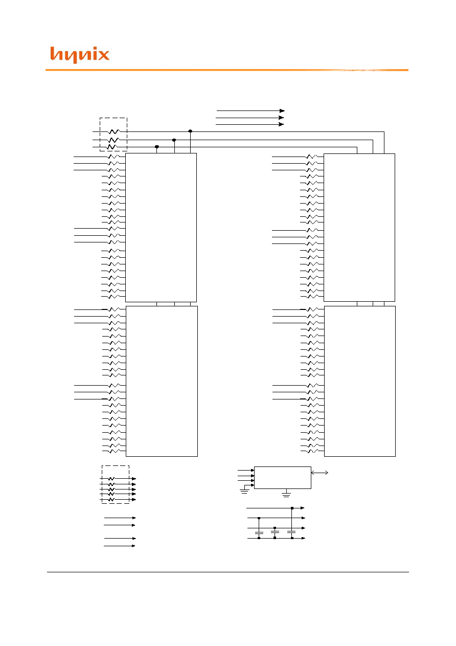
FUNCTIONAL BLOCK DIAGRAM
256MB(32Mbx64) : HYMP532S646-E3/C4
C K E 0
/S 0
O D T 0
D 0
/C S O D T C K E
D Q S 0
L D Q S
/D Q S 0
/U D Q S
D M 0
L D M
D Q 0
I/O 0
D Q 1
I/O 1
D Q 2
I/O 2
D Q 3
I/O 3
D Q 4
I/O 4
D Q 5
I/O 5
D Q 6
I/O 6
I/O 7
D Q 7
D Q S 1
U D Q S
/D Q S 1
/U D Q S
D M 1
U D M
D Q 8
D Q 8
D Q 1 0
D Q 1 1
D Q 1 2
D Q 1 3
D Q 1 4
D Q 1 5
D 1
/C S O D T C K E
D Q S 2
L D Q S
/D Q S 2
/L D Q S
D M 2
L D M
D Q 1 6
I/O 0
D Q 1 7
I/O 1
D Q 1 8
I/O 2
D Q 1 9
I/O 3
D Q 2 0
I/O 4
D Q 2 1
I/O 5
D Q 2 2
I/O 6
I/O 7
D Q 2 3
D Q S 3
U D Q S
/D Q S 3
/U D Q S
D M 3
U D M
D Q 2 4
D Q 2 5
D Q 2 6
D Q 2 7
D Q 2 8
D Q 2 9
D Q 3 0
D Q 3 1
S C L
S D A
A 0
A 1
A 2
S e r ia l P D
S C L
S D A
W P
S A 0
S A 1
D Q S 5
/D Q S 5
D M 5
D Q 4 0
D Q 4 1
D Q 4 2
D Q 4 3
D Q 4 4
D Q 4 5
D Q 4 6
D Q 4 7
D 3
/C S O D T C K E
D Q S 6
L D Q S
/D Q S 6
/L D Q S
D M 6
L D M
D Q 4 8
I/O 0
D Q 4 9
I/O 1
D Q 5 0
I/O 2
D Q 5 1
I/O 3
D Q 5 2
I/O 4
D Q 5 3
I/O 5
D Q 5 4
I/O 6
I/O 7
D Q 5 5
D Q S 7
U D Q S
/D Q S 7
/U D Q S
D M 7
U D M
D Q 5 6
D Q 5 7
D Q 5 8
D Q 5 9
D Q 6 0
D Q 6 1
D Q 6 2
D Q 6 3
D 2
/C S O D T C K E
D Q S 4
L D Q S
/D Q S 4
/L D Q S
D M 4
L D M
D Q 3 2
I/O 0
D Q 3 3
I/O 1
D Q 3 4
I/O 2
D Q 3 5
I/O 3
D Q 3 6
I/O 4
D Q 3 7
I/O 5
D Q 3 8
I/O 6
I/O 7
D Q 3 9
/S 1
N .C .
O D T 1
N .C .
C K E 1
N .C .
3
+ /-
5 %
B A 0 -B A 1
3
+ /- 5 %
A 0 - A N
/R A S
/C A S
/W E
S D R A M S D 0 -3
S D R A M S D 0 -3
S D R A M S D 0 -3
S D R A M S D 0 -3
S D R A M S D 0 -3
2 lo a d s
C K 0
/C K 0
2 lo a d s
C K 1
/C K 1
I/O 8
I/O 9
I/O 1 0
I/O 1 1
I/O 1 2
I/O 1 3
I/O 1 4
I/O 1 5
I/O 8
I/O 9
I/O 1 0
I/O 1 1
I/O 1 2
I/O 1 3
I/O 1 4
I/O 1 5
I/O 8
I/O 9
I/O 1 0
I/O 1 1
I/O 1 2
I/O 1 3
I/O 1 4
I/O 1 5
U D Q S
/U D Q S
U D M
I/O 8
I/O 9
I/O 1 0
I/O 1 1
I/O 1 2
I/O 1 3
I/O 1 4
I/O 1 5
V
D D
S P D
V
D D
V
R E F
V
S S
S e r ia l P D
S D R A M S D O - D 3
S D R A M S D O - D 3 , V D D a n d V D D Q
S D R A M S D O - D 3 , S P D
1 . R e s is to r v a lu e s a r e 2 2 O h m + /- 5 %
N o te s :