Rev. 0.95 / July.01 2
RIMM
Module
with 256/288Mb RDRAMs Preliminary
TM
`
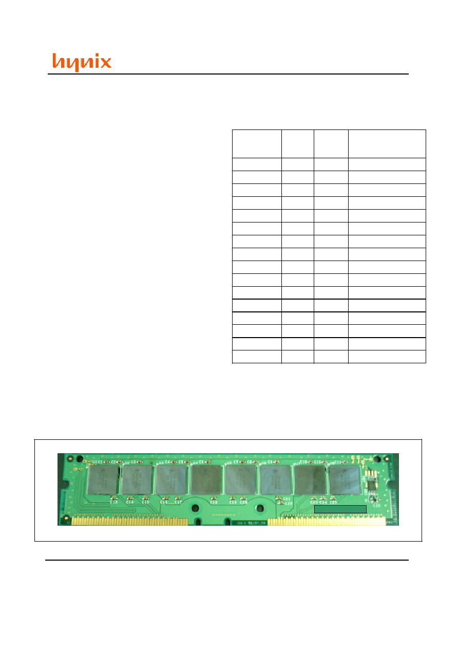
Figure 1: Rambus RIMM Module without heat spreader
Overview
The Rambus
�
RIMM
TM
module is a general purpose
high-performance memory subsystem suitable for use
in a broad range of applications including computer
memory, personal computers, workstations, and other
applications where high bandwidth and low latency are
required.
The Rambus RIMM module consist of 256/288Mb
Direct Rambus DRAM devices. These are extremely
high-speed CMOS DRAMs organized as 16M words
by 16/18 bits. The use of Rambus Signaling Level
(RSL) technology permits 600MHz ,711MHz or
800MHz transfer rates while using conventional
system and board design technologies. RDRAM
devices are capable of sustained data transfers at 1.25
ns per two bytes (10ns per 16 bytes).
The RDRAM architecture enables the highest
sustained bandwidth for multiple, simultaneous
randomly addressed memory transactions. The
separate control and data buses with independent row
and column control yield over 95% bus efficiency. The
Direct RDRAM's 32-banks architecture supports up to
four simultaneous transactions per device.
Features
w
High speed 800,711 and 600 MHz RDRAM storage
w
184 edge connector pads with 1 mm pad spacing
w
Maximum module PCB size: 133.5mm x 34.93mm x
1.37mm(5.21" x 1.375" x 0.05")
w
Gold plated edge connector pad contacts
w
Serial Presence Detect(SPD) support
w
Operates from a 2.5 volt supply (
�
5%)
w
Powerdown self refresh modes
w
�
BGA Package (92 balls)
w
Separate Row and Column buses for higher
efficiency
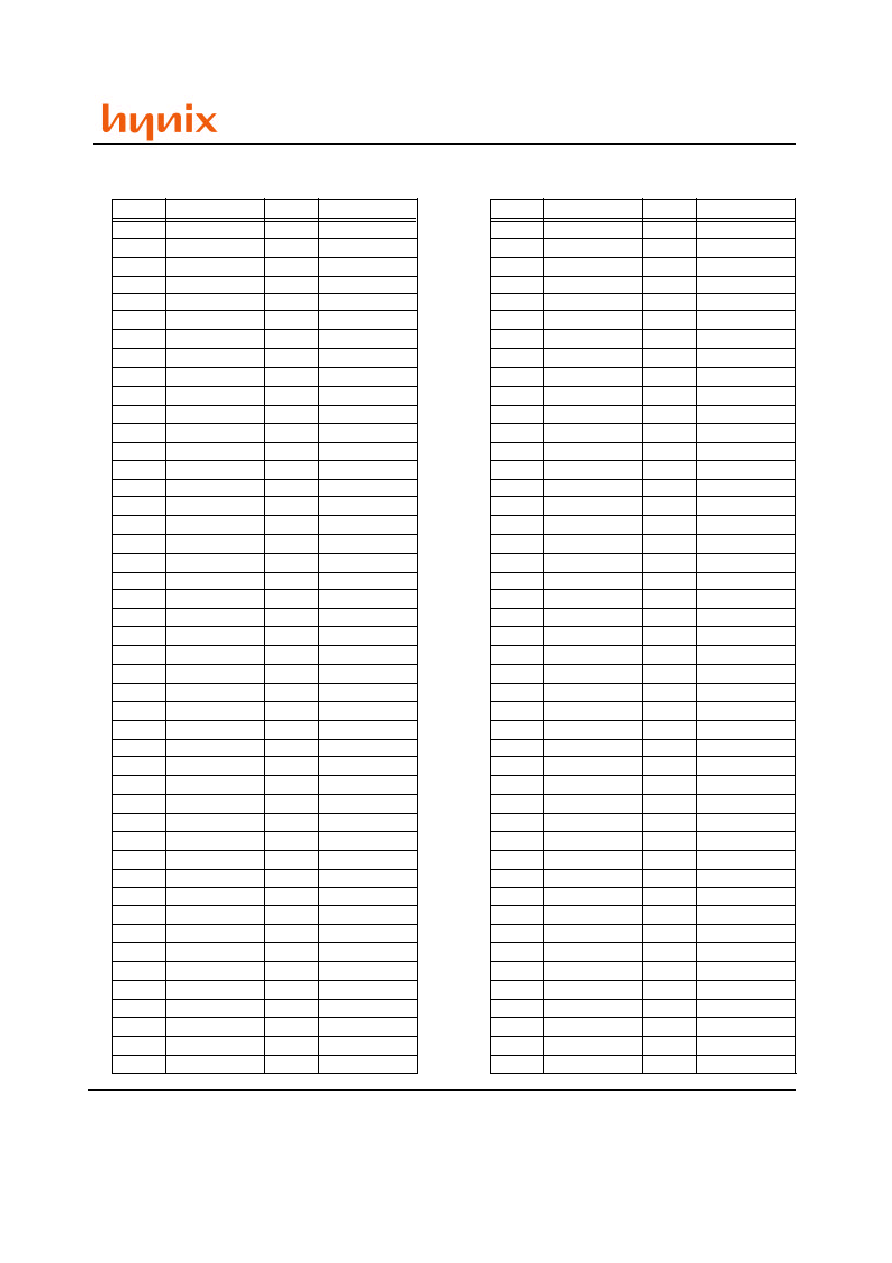
Key Timing Parameters/Part Numbers
The following table lists the frequency and latency bins
available from RIMM modules.
Form Factor
The Rambus RIMM modules are offered in a 184-pad
1mm edge connector pad pitch from factor suitable for
either 184 or 168 contact RIMM connectors. The
RIMM module is suitable for desktop and other system
applications. Figure 1 below, shows an eight device
Rambus RIMM module without heat spreader.
Table 1: Part Number by Frequency and Latency
Organization
I/O Freq.
MHz
t rac (
Row
Access
Time
) ns
32M x 16/18
600
53
32M x 16/18
711
45
32M x 16/18
800
40
128M x 16/18
600
53
128M x 16/18
711
45
128M x 16/18
800
45
128M x 16/18
800
40
32M x 16/18
800
45
256M x 16/18
600
53
256M x 16/18
711
45
256M x 16/18
800
45
256M x 16/18
800
40
Part Number
HYMR23216(18)H-653
HYMR23216(18)H-745
HYMR23216(18)H-840
HYMR212816(18)H-653
HYMR212816(18)H-745
HYMR212816(18)H-845
HYMR212816(18)H-840
HYMR23216(18)H-845
HYMR225616(18)H-653
HYMR225616(18)H-745
HYMR225616(18)H-845
HYMR225616(18)H-840
64M x 16/18
600
53
64M x 16/18
711
45
64M x 16/18
800
40
64M x 16/18
800
45
HYMR26416(18)H-653
HYMR26416(18)H-745
HYMR26416(18)H-840
HYMR26416(18)H-845
Rev. 0.95 / July.01 4
RIMM
Module
with 256/288Mb RDRAMs Preliminary
TM
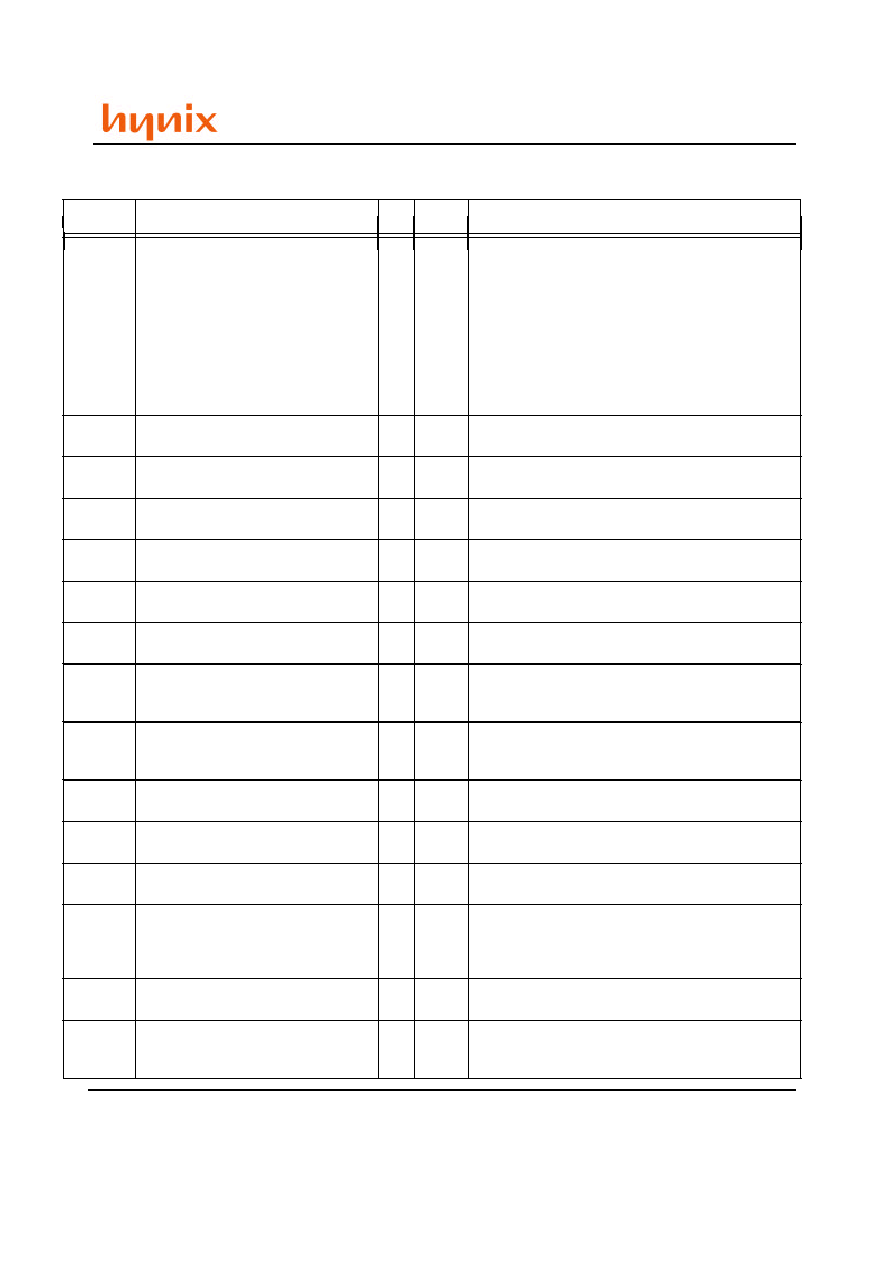
Table 3: Module Connector Pad Description
Module Connector Pads
I/O
Signal
Type
Description
A1, A3, A5, A7, A9, A11, A13, A15,
A17, A19, A21, A23, A25, A27, A29,
A31, A33, A39, A52, A60, A62, A64,
A66, A68, A70, A72, A74, A76, A78,
A80, A82, A84, A86, A88, A90, A92,
B1, B3, B5, B7, B9, B11, B13, B15,
B17, B19, B21, B23, B25, B27, B29,
B31, B33, B39, B52, B60, B62, B64,
B66, B68, B70, B72, B74, B76, B78,
B80, B82, B84, B86, B88, B90, B92
Gnd
Ground reference for RDRAM core and interface.
72 PCB connector pads.
B10
I
LCFM
RSL
Clock from master. Interface clock used for receiving
RSL signals from the Channel. Positive polarity
.
B12
I
LCFMN
RSL
Clock from master. Interface clock used for receiving
RSL signals from the Channel. Negative polarity.
B81
I
RCFMN
RSL
Clock from master. Interface clock used for receiv-
ing RSL signals from the Channel. Negative polar-
ity.
B34
I
LCMD
V
CMOS
Serial Command used to read from and write to the
control registers. Also used for power management.
A20, B20, A22, B22, A24
I
LCOL4..
LCOL0
RSL
Column bus. 5-bit bus containing control and address
information for column accesses.
A14
I
LCTM
RSL
Clock to master. Interface clock used for transmit-
ting RSL signals to the Channel. Positive polarity.
A12
I
LCTMN
RSL
Clock to master. Interface clock used for transmit-
ting RSL signals to the Channel. Negative polarity.
A2, B2, A4, B4, A6, B6, A8, B8, A10
I/O
LDQA8..
LDQA0
RSL
Data bus A. A 9-bit bus carrying a byte of read or
write data between the Channel and the RDRAM.
LDQA8 is non-functional on x16 RDRAM devices.
B32, A32, B30, A30, B28, A28, B26,
A26, B24
I/O
LDQB8..
LDQB0
RSL
Data bus B. A 9-bit bus carrying a byte of read or
write data between the Channel and the RDRAM.
LDQB8 is non-functional on x16 RDRAM devices.
B16, A18, B18
I
LROW2..
LROW0
RSL
Row bus. 3-bit bus containing control and address
information for row accesses.
A34
I
LSCK
V
CMOS
Serial Clock input. Clock source used to read from
and write to the RDRAM control registers.
A16, B14, A38, B38, A40, B40, A77,
B79
NC
These pads are not connected. These 8 connector
pads are reserved for future use.
A43, B43, A44, B44, A45, B45, A46,
B46, A47, B47, A48, B48, A49, B49,
A50, B50
NC
These pads are not connected. These 16connector
pads art reserved for future use. The 168 contact
RIMM connector does not connect to these PCB
pads.
B83
I
RCFM
RSL
Clock from master. Interface clock used for receiv-
ing RSL signals from the Channel. Positive polarity.
Rev. 0.95 / July.01 5
RIMM
Module
with 256/288Mb RDRAMs Preliminary
TM
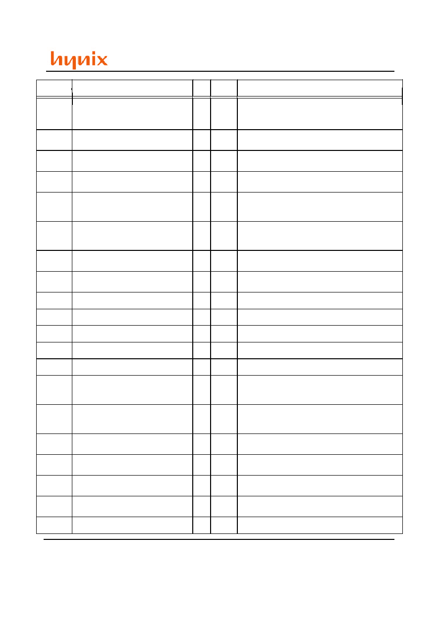
Module Connector Pads
I/O
Signal
Type
Description
B59
RCMD
Serial Command Input used to read from and write
to the control registers. Also used for power
management.
I
V
CMOS
A73, B73, A71, B71, A69
I
RCOL4..
RCOL0
RSL
Column bus. 5-bit bus containing control and
address information for column accesses.
A41, A42, A54, A58, B41, B42, B54,
B58
I
Vdd
Supply voltage for the RDRAM core and interface
logic.
A79
I
RCTM
RSL
Clock to master. Interface clock used for transmit-
ting RSL signals to the Channel. Positive polarity.
A81
I
RCTMN
RSL
Clock to master. Interface clock used for transmit-
ting RSL signals to the Channel. Negative polarity.
A91, B91, A89, B89, A87, B87, A85,
B85, A83
I/O
RDQA8..
RDQA0
RSL
Data bus A. A 9-bit bus carrying a byte of read or
write data between the Channel and the RDRAM.
RDQA8 is non-functional on x16 RDRAM devices.
B61, A61, B63, A63, B65, A65, B67,
A67, B69
I/O
RDQB8..
RDQB0
RSL
Data bus B. A 9-bit bus carrying a byte of read or
write data between the Channel and the RDRAM.
RDQB8 is non-functional on x16 RDRAM devices.
B77, A75, B75
I
RROW2..
RROW0
RSL
Row bus. 3-bit bus containing control and address
information for row accesses.
A59
I
RSCK
V
CMOS
Serial Clock input. Clock source used to read from
and write to the RDRAM control registers.
B53
I
SA0
SV
DD
Serial Presence Detect Address 0.
B55
I
SA1
SV
DD
Serial Presence Detect Address 1.
B57
I
SA2
SV
DD
Serial Presence Detect Address 2.
A53
I
SCL
SV
DD
Serial Presence Detect Clock.
A55
I/O
SDA
SV
DD
Serial Presence Detect Data (Open Collector I/O)
B36
I/O
SIN
V
CMOS
Serial I/O for reading from and writing to the control
registers. Attaches to SIO0 of the first RDRAM on
the module.
A36
I/O
SOUT
V
CMOS
Serial I/O for reading from and writing to the control
registers. Attaches to SIO1 of the last RDRAM on
the module.
A56, B56
SV
DD
SPD Voltage. Used for signals SCL, SDA, SWE,
SA0, SA1 and SA2.
A57
I
SWP
SV
DD
Serial Presence Detect Write Protect (active high).
When low, the SPD can be written as well as read.
A35, B35, A37, B37
V
CMOS
CMOS I/O Voltage. Used for signals CMD, SCK,
SIN, SOUT.
A51, B51
Vref
Logic threshold reference voltage for RSL signals.