 | –≠–ї–µ–Ї—В—А–Њ–љ–љ—Л–є –Ї–Њ–Љ–њ–Њ–љ–µ–љ—В: 405GP | –°–Ї–∞—З–∞—В—М:  PDF PDF  ZIP ZIP |

4/14/03
PowerPC 405GP Embedded Processor Data Sheet
Page 1 of 58
Features
Ј IBM PowerPC
405 32-bit RISC processor core
operating up to 266MHz
Ј PC-133 synchronous DRAM (SDRAM) interface
- 32-bit interface for non-ECC applications
- 40-bit interface serves 32 bits of data plus 8
check bits for ECC applications
Ј 4 KB on-chip memory (OCM)
Ј External peripheral bus
- Flash ROM/Boot ROM interface
- Direct support for 8-, 16-, or 32-bit SRAM
and external peripherals
- Up to eight devices
- External Mastering supported
Ј DMA support for external peripherals, internal
UART and memory
- Scatter-gather chaining supported
- Four channels
Ј PCI Revision 2.2 compliant interface (32-bit, up
to 66MHz)
- Synchronous or asynchronous PCI Bus
interface
- Internal or external PCI Bus Arbiter
Ј Ethernet 10/100 Mbps (full-duplex) support with
media independent interface (MII)
Ј Programmable interrupt controller supports
seven external and 19 internal edge triggered or
level-sensitive interrupts
Ј Programmable timers
Ј Two serial ports (16550 compatible UART)
Ј One IIC interface
Ј General purpose I/O (GPIO) available
Ј Supports JTAG for board level testing
Ј Internal processor local Bus (PLB) runs at
SDRAM interface frequency
Ј Supports PowerPC processor boot from PCI
memory
Description
Designed specifically to address embedded
applications, the PowerPC 405GP (PPC405GP)
provides a high-performance, low-power solution
that interfaces to a wide range of peripherals by
incorporating on-chip power management features
and lower power dissipation requirements.
This chip contains a high-performance RISC
processor core, SDRAM controller, PCI bus
interface, Ethernet interface, control for external
ROM and peripherals, DMA with scatter-gather
support, serial ports, IIC interface, and general
purpose I/O.
Technology: IBM CMOS SA-12E, 0.25
µ
m
(0.18
µ
m L
eff
)
Package: 456-ball (35mm or 27mm), or 413-ball
(25mm) enhanced plastic ball grid array (E-PBGA)
Power (typical): 1.5W at 200MHz, 2 W at 266MHz

PowerPC 405GP Embedded Processor Data Sheet
Page 2 of 58
4/14/03
Contents
Ordering, PVR, and JTAG Information . . . . . . . . . . . . . . . . . . . . . . . . . . . . . . . . . . . . . . . . . . . . . . . . . . . . . . 4
Address Map Support . . . . . . . . . . . . . . . . . . . . . . . . . . . . . . . . . . . . . . . . . . . . . . . . . . . . . . . . . . . . . . . . . . . 6
On-Chip Memory (OCM) . . . . . . . . . . . . . . . . . . . . . . . . . . . . . . . . . . . . . . . . . . . . . . . . . . . . . . . . . . . . . . . . . 8
PLB to PCI Interface . . . . . . . . . . . . . . . . . . . . . . . . . . . . . . . . . . . . . . . . . . . . . . . . . . . . . . . . . . . . . . . . . . . . 8
SDRAM Memory Controller . . . . . . . . . . . . . . . . . . . . . . . . . . . . . . . . . . . . . . . . . . . . . . . . . . . . . . . . . . . . . . 9
External Peripheral Bus Controller (EBC) . . . . . . . . . . . . . . . . . . . . . . . . . . . . . . . . . . . . . . . . . . . . . . . . . . . . 9
DMA Controller . . . . . . . . . . . . . . . . . . . . . . . . . . . . . . . . . . . . . . . . . . . . . . . . . . . . . . . . . . . . . . . . . . . . . . . 10
Serial Interface . . . . . . . . . . . . . . . . . . . . . . . . . . . . . . . . . . . . . . . . . . . . . . . . . . . . . . . . . . . . . . . . . . . . . . . 11
IIC Bus Interface . . . . . . . . . . . . . . . . . . . . . . . . . . . . . . . . . . . . . . . . . . . . . . . . . . . . . . . . . . . . . . . . . . . . . . 11
General Purpose IO (GPIO) Controller . . . . . . . . . . . . . . . . . . . . . . . . . . . . . . . . . . . . . . . . . . . . . . . . . . . . . 12
Universal Interrupt Controller (UIC) . . . . . . . . . . . . . . . . . . . . . . . . . . . . . . . . . . . . . . . . . . . . . . . . . . . . . . . 12
10/100 Mbps Ethernet MAC . . . . . . . . . . . . . . . . . . . . . . . . . . . . . . . . . . . . . . . . . . . . . . . . . . . . . . . . . . . . . 12
JTAG . . . . . . . . . . . . . . . . . . . . . . . . . . . . . . . . . . . . . . . . . . . . . . . . . . . . . . . . . . . . . . . . . . . . . . . . . . . . . . . 12
Signal List . . . . . . . . . . . . . . . . . . . . . . . . . . . . . . . . . . . . . . . . . . . . . . . . . . . . . . . . . . . . . . . . . . . . . . . . . . . 32
Spread Spectrum Clocking . . . . . . . . . . . . . . . . . . . . . . . . . . . . . . . . . . . . . . . . . . . . . . . . . . . . . . . . . . . . . . 47
Strapping . . . . . . . . . . . . . . . . . . . . . . . . . . . . . . . . . . . . . . . . . . . . . . . . . . . . . . . . . . . . . . . . . . . . . . . . . . . . 55
Tables
System Memory Address Map . . . . . . . . . . . . . . . . . . . . . . . . . . . . . . . . . . . . . . . . . . . . . . . . . . . . . . . . . . . . 6
DCR Address Map . . . . . . . . . . . . . . . . . . . . . . . . . . . . . . . . . . . . . . . . . . . . . . . . . . . . . . . . . . . . . . . . . . . . . 7
Signals Listed Alphabetically . . . . . . . . . . . . . . . . . . . . . . . . . . . . . . . . . . . . . . . . . . . . . . . . . . . . . . . . . . . . 16
Signals Listed by Ball Assignment--413-Ball Package . . . . . . . . . . . . . . . . . . . . . . . . . . . . . . . . . . . . . . . . 26
Signals Listed by Ball Assignment--456-Ball Package . . . . . . . . . . . . . . . . . . . . . . . . . . . . . . . . . . . . . . . . 29
Pin Summary . . . . . . . . . . . . . . . . . . . . . . . . . . . . . . . . . . . . . . . . . . . . . . . . . . . . . . . . . . . . . . . . . . . . . . . . 32
Signal Functional Description . . . . . . . . . . . . . . . . . . . . . . . . . . . . . . . . . . . . . . . . . . . . . . . . . . . . . . . . . . . . 34
Absolute Maximum Ratings . . . . . . . . . . . . . . . . . . . . . . . . . . . . . . . . . . . . . . . . . . . . . . . . . . . . . . . . . . . . . 42
Package Thermal Specifications . . . . . . . . . . . . . . . . . . . . . . . . . . . . . . . . . . . . . . . . . . . . . . . . . . . . . . . . . . 42
Recommended DC Operating Conditions . . . . . . . . . . . . . . . . . . . . . . . . . . . . . . . . . . . . . . . . . . . . . . . . . . . 43
Input Capacitance . . . . . . . . . . . . . . . . . . . . . . . . . . . . . . . . . . . . . . . . . . . . . . . . . . . . . . . . . . . . . . . . . . . . . 44
DC Electrical Characteristics . . . . . . . . . . . . . . . . . . . . . . . . . . . . . . . . . . . . . . . . . . . . . . . . . . . . . . . . . . . . 45
Clocking Specifications . . . . . . . . . . . . . . . . . . . . . . . . . . . . . . . . . . . . . . . . . . . . . . . . . . . . . . . . . . . . . . . . . 46
Peripheral Interface Clock Timings . . . . . . . . . . . . . . . . . . . . . . . . . . . . . . . . . . . . . . . . . . . . . . . . . . . . . . . . 48
I/O Specifications--All speeds . . . . . . . . . . . . . . . . . . . . . . . . . . . . . . . . . . . . . . . . . . . . . . . . . . . . . . . . . . . 50
I/O Specifications--200MHz . . . . . . . . . . . . . . . . . . . . . . . . . . . . . . . . . . . . . . . . . . . . . . . . . . . . . . . . . . . . . 53
I/O Specifications--266MHz . . . . . . . . . . . . . . . . . . . . . . . . . . . . . . . . . . . . . . . . . . . . . . . . . . . . . . . . . . . . . 54
PPC405GP Strapping Pin Assignments . . . . . . . . . . . . . . . . . . . . . . . . . . . . . . . . . . . . . . . . . . . . . . . . . . . . 55

PowerPC 405GP Embedded Processor Data Sheet
4/14/03
Page 3 of 58
Figures
PPC405GP Embedded Controller Functional Block Diagram . . . . . . . . . . . . . . . . . . . . . . . . . . . . . . . . . . . . 5
25mm, 413-Ball E-PBGA Package . . . . . . . . . . . . . . . . . . . . . . . . . . . . . . . . . . . . . . . . . . . . . . . . . . . . . . . . 13
27mm, 456-Ball E-PBGA Package . . . . . . . . . . . . . . . . . . . . . . . . . . . . . . . . . . . . . . . . . . . . . . . . . . . . . . . . 14
35mm, 456-Ball E-PBGA Package . . . . . . . . . . . . . . . . . . . . . . . . . . . . . . . . . . . . . . . . . . . . . . . . . . . . . . . . 15
5V-Tolerant Input Current . . . . . . . . . . . . . . . . . . . . . . . . . . . . . . . . . . . . . . . . . . . . . . . . . . . . . . . . . . . . . . . 44
Input Setup and Hold Waveform . . . . . . . . . . . . . . . . . . . . . . . . . . . . . . . . . . . . . . . . . . . . . . . . . . . . . . . . . 49
Output Delay and Float Timing Waveform . . . . . . . . . . . . . . . . . . . . . . . . . . . . . . . . . . . . . . . . . . . . . . . . . . 49
PowerPC 405GP Embedded Processor Data Sheet
Page 4 of 58
4/14/03
Ordering, PVR, and JTAG Information
This section provides the part number nomenclature. For availability, contact your local IBM sales office.
The part number contains a part modifier. Included in the modifier is a revision code. This refers to the die
mask revision number and is specified in the part numbering scheme for identification purposes only.
The PVR (Processor Version Register) is software accessible and contains additional information about the
revision level of the part. Refer to the
PowerPC 405GP Embedded Processor User's Manual for details on the
register content.
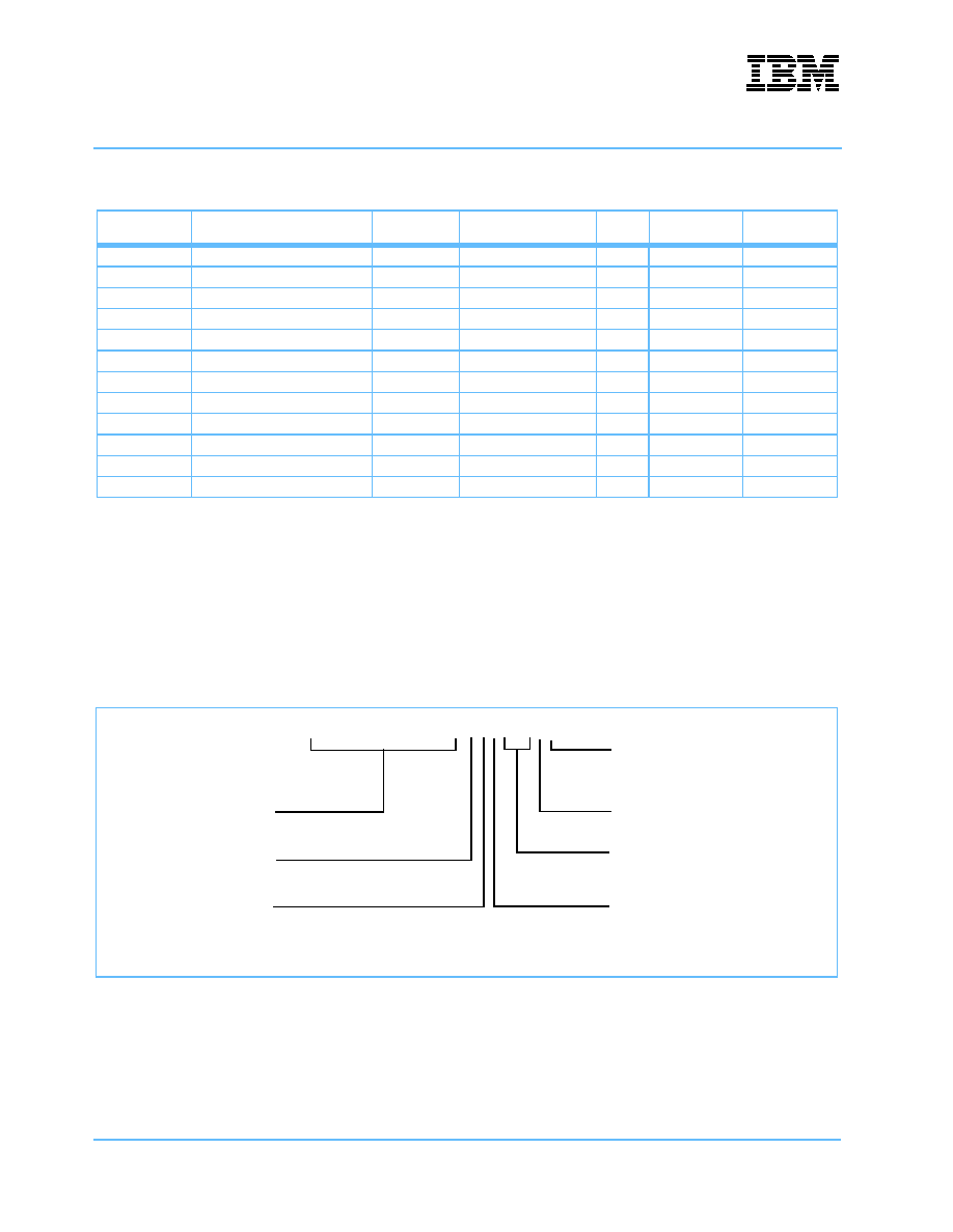
Order Part Number Key
Product Name
Order Part Number
1
Processor
Frequency
Package
Rev
Level
PVR Value
JTAG ID
PPC405GP
IBM25PPC405GP-3BE200C
200 MHz
35mm, 456 E-PBGA
E
0x40110145
0x42050049
PPC405GP
IBM25PPC405GP3BE200CZ
200 MHz
35mm, 456 E-PBGA
E
0x40110145
0x42050049
PPC405GP
IBM25PPC405GP-3DE200C
200 MHz
27mm, 456 E-PBGA
E
0x40110145
0x42050049
PPC405GP
IBM25PPC405GP-3DE200CZ
200 MHz
27mm, 456 E-PBGA
E
0x40110145
0x42050049
PPC405GP
IBM25PPC405GP-3EE200C
200 MHz
25mm, 413 E-PBGA
E
0x40110145
0x42050049
PPC405GP
IBM25PPC405GP-3EE200CZ
200 MHz
25mm, 413 E-PBGA
E
0x40110145
0x42050049
PPC405GP
IBM25PPC405GP-3BE266C
266 MHz
35mm, 456 E-PBGA
E
0x40110145
0x42050049
PPC405GP
IBM25PPC405GP-3BE266CZ
266 MHz
35mm, 456 E-PBGA
E
0x40110145
0x42050049
PPC405GP
IBM25PPC405GP-3DE266C
266 MHz
27mm, 456 E-PBGA
E
0x40110145
0x42050049
PPC405GP
IBM25PPC405GP-3DE266CZ
266 MHz
27mm, 456 E-PBGA
E
0x40110145
0x42050049
PPC405GP
IBM25PPC405GP-3EE266C
266 MHz
25mm, 413 E-PBGA
E
0x40110145
0x42050049
PPC405GP
IBM25PPC405GP-3EE266CZ
266 MHz
25mm, 413 E-PBGA
E
0x40110145
0x42050049
Note 1: Z at the end of the Order Part Number indicates a tape and reel shipping package. Otherwise, the chips are shipped in a tray.
IBM Part Number
IBM25PPC405GP-3BE200Cx
Package
Processor Speed
Grade 3 Reliability
Operational Case Temperature
Revision Level
Shipping Package
Blank = Tray
Z = Tape and reel
(-40 ∞C to +85 ∞C)
Range
200 MHz
266 MHz
B: 35mm, 456 E-PBGA
D: 27mm, 456 E-PBGA
E: 25mm, 413 E-PBGA
PowerPC 405GP Embedded Processor Data Sheet
4/14/03
Page 5 of 58
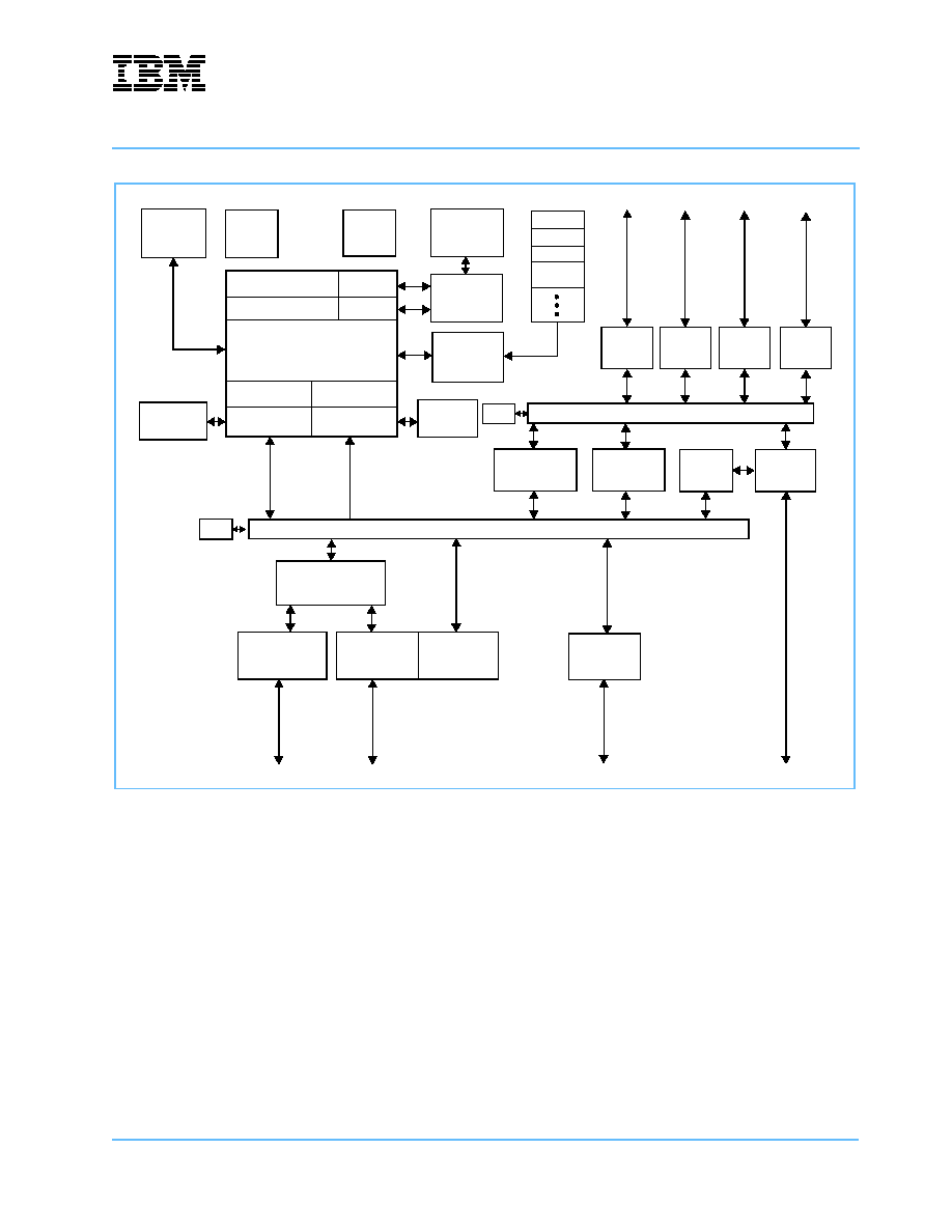
PPC405GP Embedded Controller Functional Block Diagram
The PPC405GP is designed using the IBM Microelectronics Blue Logic
TM
methodology in which major
functional blocks are integrated together to create an application-specific ASIC product. This approach
provides a consistent way to create complex ASICs using IBM CoreConnect
TM
Bus Architecture.
PPC405
Processor Core
DOCM
IOCM
DCU
ICU
OCM
Control
OCM
SRAM
DCR Bus
16KB
On-chip Peripheral Bus (OPB)
GPIO
IIC
UART
UART
MAL
Ethernet
DMA
Bridge
Processor Local Bus (PLB)
SDRAM
PCI Bridge
Code
Decompression
External
Bus
Controller
Controller
Clock
Control
Reset
Power
Mgmt
JTAG
Trace
Timers
MMU
MII
Controller
OPB
Interrupt
Controller
Arb
32-bit addr
32-bit data
13-bit addr
32-bit data
External
Bus Master
Controller
Universal
I-Cache
D-Cache
(4-Channel)
(CodePack
)
66 MHz max (async)
DCRs
33 MHz max (sync)
8KB
Arb