
crrh2516.04
12/00
©IBM Corporation. All rights reserved.
Use is further subject to the provisions at the end of this document.
Page 1 of 24
IBM0418A81XLAB
IBM0436A81XLAB
IBM0418A41XLAB
IBM0436A41XLAB
Preliminary
8Mb (256Kx36 & 512Kx18) and 4Mb (128Kx36 & 256Kx18) SRAM
Features
∑ 8Mb: 256K x 36 or 512K x 18 organizations
4Mb: 128K x 36 or 256K x 18 organizations
∑ 0.25 Micron CMOS technology
∑ Synchronous Pipeline Mode of Operation with
Self-Timed Late Write
∑ Single Differential HSTL Clock
∑ +2.5V Power Supply, Ground, 1.6V V
DDQ
, and
0.95V V
REF
∑ HSTL Input and Output levels
∑ Registered Addresses, Write Enables, Synchro-
nous Select, and Data Ins
∑ Registered Outputs
∑ Common I/O
∑ Asynchronous Output Enable and Power Down
Inputs
∑ Boundary Scan using limited set of JTAG
1149.1 functions
∑ Byte Write Capability and Global Write Enable
∑ 7 x 17 Bump Ball Grid Array Package with
SRAM JEDEC Standard Pinout and Boundary
SCAN Order
∑ Programmable Impedance Output Drivers
Description
The 4Mb and 8Mb SRAM
S
--IBM0436A41XLAB,
IBM0418A41XLAB, IBM0418A81XLAB, and
IBM0436A81XLAB--are Synchronous Pipeline
Mode, high-performance CMOS Static Random
Access Memories that are versatile, have wide I/O,
and can achieve 3ns cycle times. Differential K
clocks are used to initiate the read/write operation
and all internal operations are self-timed. At the ris-
ing edge of the K clock, all Addresses, Write-
Enables, Sync Select, and Data Ins are registered
internally. Data Outs are updated from output regis-
ters off the next rising edge of the K clock. An inter-
nal Write buffer allows write data to follow one cycle
after addresses and controls. The chip is operated
with a single +2.5V power supply and is compatible
with HSTL I/O interfaces.
.
IBM0418A81XLAB
IBM0436A81XLAB
IBM0418A41XLAB
IBM0436A41XLAB
8Mb (256Kx36 & 512Kx18) and 4Mb (128Kx36 & 256Kx18) SRAM
Preliminary
©IBM Corporation. All rights reserved.
Use is further subject to the provisions at the end of this document.
Page 2 of 24
crrh2516.04
12/00
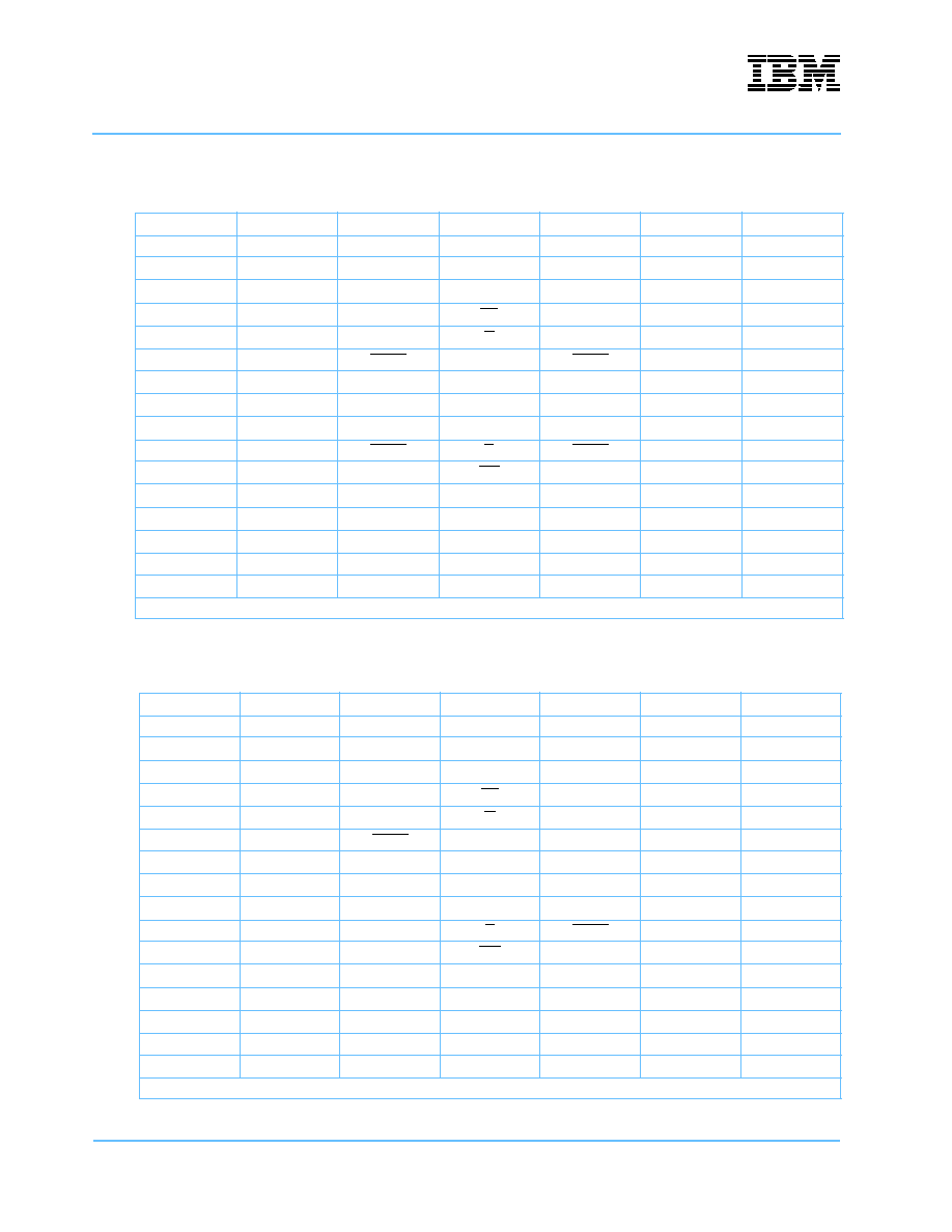
x36 BGA Pinout (Top View)
1
2
3
4
5
6
7
A
V
DDQ
SA
SA
NC
SA
SA
V
DDQ
B
NC
NC
SA
NC
SA
NC,SA(8Mb)
NC
C
NC
SA
SA
V
DD
SA
SA
NC
D
DQ19
DQ18
V
SS
ZQ
V
SS
DQ9
DQ10
E
DQ22
DQ20
V
SS
SS
V
SS
DQ11
DQb13
F
V
DDQ
DQ21
V
SS
G
V
SS
DQ12
V
DDQ
G
DQ24
DQ23
SBWc
NC
SBWb
DQ14
DQb15
H
DQ25
DQ26
V
SS
NC
V
SS
DQ17
DQb16
J
V
DDQ
V
DD
V
REF
V
DD
V
REF
V
DD
V
DDQ
K
DQ34
DQ35
V
SS
K
V
SS
DQ8
DQ7
L
DQ33
DQ32
SBWd
K
SBWa
DQ5
DQ6
M
V
DDQ
DQ30
V
SS
SW
V
SS
DQ3
V
DDQ
N
DQ31
DQ29
V
SS
SA
V
SS
DQ2
DQ4
P
DQ28
DQ27
V
SS
SA
V
SS
DQ0
DQ1
R
NC
SA
M1*
V
DD
M2*
SA
NC
T
NC
NC
SA
SA
SA
NC
ZZ
U
V
DDQ
TMS
TDI
TCK
TDO
NC
V
DDQ
Note: * M1 and M2 are clock mode pins. For this application, M1 and M2 need to connect to V
SS
and V
DD
, respectively.
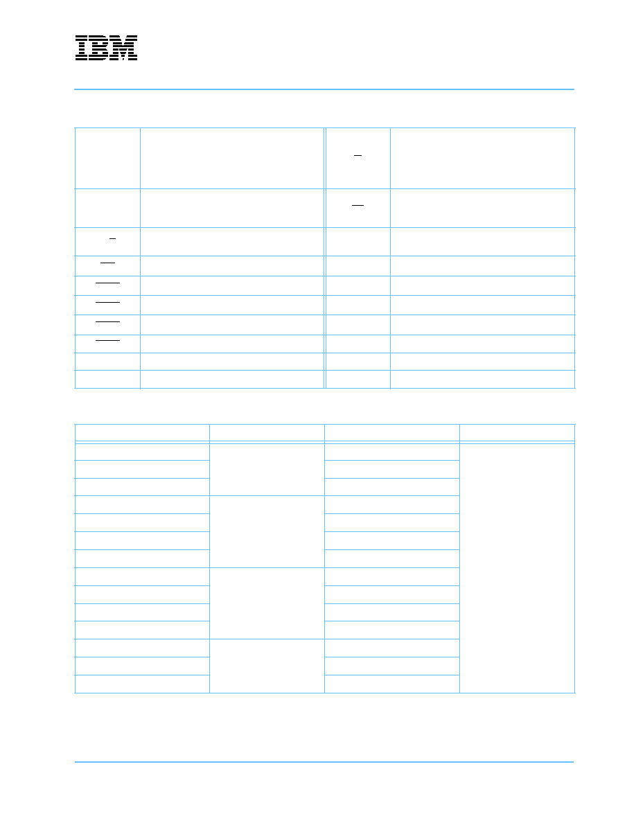
x18 BGA Pinout (Top View)
1
2
3
4
5
6
7
A
V
DDQ
SA
SA
NC
SA
SA
V
DDQ
B
NC
NC
SA
NC
SA
NC,SA(8Mb)
NC
C
NC
SA
SA
V
DD
SA
SA
NC
D
DQ14
NC
V
SS
ZQ
V
SS
DQ0
NC
E
NC
DQ15
V
SS
SS
V
SS
NC
DQ1
F
V
DDQ
NC
V
SS
G
V
SS
DQ2
V
DDQ
G
NC
DQ16
SBWb
NC
NC
NC
DQ3
H
DQ17
NC
V
SS
NC
V
SS
DQ4
NC
J
V
DDQ
V
DD
V
REF
V
DD
V
REF
V
DD
V
DDQ
K
NC
DQ13
V
SS
K
V
SS
NC
DQ8
L
DQ12
NC
NC
K
SBWa
DQ7
NC
M
V
DDQ
DQ10
V
SS
SW
V
SS
NC
V
DDQ
N
DQ11
NC
V
SS
SA
V
SS
DQ6
NC
P
NC
DQ9
V
SS
SA
V
SS
NC
DQ5
R
NC
SA
M1
V
DD
M2
SA
NC
T
NC
SA
SA
NC
SA
SA
ZZ
U
V
DDQ
TMS
TDI
TCK
TDO
NC
V
DDQ
Note: * M1 and M2 are clock mode pins. For this application, M1 and M2 need to connect to V
SS
and V
DD
respectively.
IBM0418A81XLAB
IBM0436A81XLAB
IBM0418A41XLAB
IBM0436A41XLAB
Preliminary
8Mb (256Kx36 & 512Kx18) and 4Mb (128Kx36 & 256Kx18) SRAM
crrh2516.04
12/00
©IBM Corporation. All rights reserved.
Use is further subject to the provisions at the end of this document.
Page 3 of 24
Pin Description
SA0-SA18
Address Input
SA0-SA18 for 512K x 18
SA0-SA17 for 256K x 36
SA0-SA17 for 256K x 18
SA0-SA16 for 128K x 36
G
Asynchronous Output Enable
DQ0-DQ35
Data I/O
DQ0-DQ17 for 512K x 18
DQ0-DQ35 for 256K x 36
SS
Synchronous Select
K, K
Differential Input Register Clocks
M1, M2
Clock Mode Inputs- Selects Single or Dual Clock
Operation.
SW
Write Enable, Global
V
REF
(2)
HSTL Input Reference Voltage
SBWa
Write Enable, Byte a (DQ0-DQ8)
V
DD
Power Supply (+2.5V)
SBWb
Write Enable, Byte b (DQ9-DQ17)
V
SS
Ground
SBWc
Write Enable, Byte c (DQ18-DQ26)
V
DDQ
Output Power Supply
SBWd
Write Enable, Byte d (DQ27-DQ35)
ZZ
Synchronous Sleep Mode
TMS,TDI,TCK
IEEE 1149.1 Test Inputs (LVTTL levels)
ZQ
Output Driver Impedance Control
TDO
IEEE 1149.1 Test Output (LVTTL level)
NC
No Connect
Ordering Information
Part Number
Organization
Speed
Leads
IBM0418A41XLAB - 3
256K x 18
1.7ns Access / 3.0ns Cycle
7 x 17 BGA
IBM0418A41XLAB - 4
2.0ns Access / 4.0ns Cycle
IBM0418A41XLAB - 5
2.25ns Access /5.0ns Cycle
IBM0436A41XLAB - 3
128K x 36
1.7ns Access / 3.0ns Cycle
IBM0436A41XLAB - 3F
1.7ns Access / 3.0ns Cycle
IBM0436A41XLAB - 4
2.0ns Access / 4.0ns Cycle
IBM0436A41XLAB - 5
2.25ns Access /5.0ns Cycle
IBM0418A81XLAB - 3
512K x 18
1.7ns Access / 3.0ns Cycle
IBM0418A81XLAB - 3F
1.7ns Access / 3.0ns Cycle
IBM0418A81XLAB - 4
2.0ns Access / 4.0ns Cycle
IBM0418A81XLAB - 5
2.25ns Access /5.0ns Cycle
IBM0436A81XLAB -3
256K x 36
1.7ns Access / 3.0ns Cycle
IBM0436A81XLAB -4
2.0ns Access / 4.0ns Cycle
IBM0436A81XLAB -5
2.25ns Access /5.0ns Cycle

IBM0418A81XLAB
IBM0436A81XLAB
IBM0418A41XLAB
IBM0436A41XLAB
8Mb (256Kx36 & 512Kx18) and 4Mb (128Kx36 & 256Kx18) SRAM
Preliminary
©IBM Corporation. All rights reserved.
Use is further subject to the provisions at the end of this document.
Page 4 of 24
crrh2516.04
12/00
Block Diagram
SBW
Row Decode
Col Decode
Read/Wr Amp
DOC_Array0
SA0-SA18
K
ZZ
G
SW
SS
DQ0-DQ35
REG
REG
SBW
2:1 MUX
DOC_MUX0
WRITE1
ADD REG
WRITE0
ADD REG
READ
ADD REG
READ
WRITE
MATCH
MATCH1
LATCH
LATCH0
WR_BUF1
WR_BUF0
2:1 MUX
DOC_MUX1
2:1 MUX
DOC_MUX2
SBW0
SW0
SW1
REG
REG
DOC_
DOUT0
REG
REG
SS1
SS0

IBM0418A81XLAB
IBM0436A81XLAB
IBM0418A41XLAB
IBM0436A41XLAB
Preliminary
8Mb (256Kx36 & 512Kx18) and 4Mb (128Kx36 & 256Kx18) SRAM
crrh2516.04
12/00
©IBM Corporation. All rights reserved.
Use is further subject to the provisions at the end of this document.
Page 5 of 24
SRAM Features
Late Write
Late Write function allows for write data to be registered one cycle after addresses and controls. This feature
eliminates one bus-turnaround cycle, necessary when going from a Read to a Write operation. Late Write is
accomplished by buffering write addresses and data so that the write operation occurs during the next write
cycle. When a read cycle occurs after a write cycle, the address and write data information are stored tempo-
rarily in holding registers. During the first write cycle preceded by a read cycle, the SRAM array will be
updated with address and data from the holding registers. Read cycle addresses are monitored to determine
if read data is to be supplied from the SRAM array or the write buffer. The bypassing of the SRAM array
occurs on a byte-by-byte basis. When only one byte is written during a write cycle, read data from the last
written address will have new byte data from the write buffer and remaining bytes from the SRAM array.
Mode Control
Mode control pins M1 and M2 are used to select four different JEDEC-standard read protocols. This SRAM
supports Single Clock, Pipeline (M1 = V
SS
, M2 = V
DD
). This datasheet only describes Single Clock Pipeline
functionality. Mode control inputs must be set with power up and must not change during SRAM operation.
This SRAM is tested only in the Pipeline mode.
Sleep Mode
Sleep Mode is enabled by switching synchronous signal ZZ High. When the SRAM is in Sleep mode, the out-
puts will go to a High-Z state and the SRAM will draw standby current. SRAM data will be preserved and a
recovery time (t
ZZR
) is required before the SRAM resumes normal operation.
RQ Programmable Impedance
An external resistor, RQ, must be connected between the ZQ pin on the SRAM and V
SS
to allow for the
SRAM to adjust its output driver impedance. The value of RQ must be 5X the value of the intended line
impedance driven by the SRAM. The allowable range of RQ to guarantee impedance matching is between
175
and 350
, with the tolerance described in Programmable Impedance Output Driver DC Electrical Char-
acteristics on page 9. The RQ resistor should be placed less than two inches away from the ZQ ball on the
SRAM module. The total external capacitance (including wiring ) seen by the ZQ ball should be minimized
(less than 7.5 pF).
Programmable Impedance and Power-Up Requirements
Periodic readjustment of the output driver impedance is necessary as the impedance is greatly affected by
drifts in supply voltage and temperature. One evaluation occurs every 64 clock cycles and each evaluation
may move the output driver impedance level only one step at a time towards the optimum level. The output
driver has 32 discrete binary weighted steps. The impedance update of the output driver occurs when the
SRAM is in High-Z. Write and Deselect operations will synchronously switch the SRAM into and out of High-
Z, therefore triggering an update. The user may choose to invoke asynchronous G updates by providing a G
setup and hold about the K clock to guarantee the proper update. There are no power-up requirements for
the SRAM; however, to guarantee optimum output driver impedance after power up, the SRAM needs 4096
clock cycles followed by a Low-Z to High-Z transition.
Power-Up and Power-Down Sequencing
The Power supplies need to be powered up in the following order: V
DD
, V
DDQ
, V
REF
, and Inputs. The power-
down sequencing must be the reverse. V
DDQ
can be allowed to exceed V
DD
by no more than 0.6V.