
IBM043616CBLBC
IBM041816CBLBC
16Mb (512K x 36 & 1M x 18) SRAM
CBLBCds.fm.00
June 3, 2002
Page 1 of 25
Features
� 512K x 36 or 1M x 18 organization
� CMOS technology
� Double-data-rate and single-data-rate synchro-
nous mode of operation
� Pipeline mode of operation
� Self-timed late write with full data coherency
� Single differential clock
� 1.8V high-speed transceiver logic (HSTL) I/O
� 2.5V power supply, 1.8V V
DDQ
� Registered addresses, controls, and data-ins
� Burst mode of operation
� Common I/O
� Asynchronous output enable
� Boundary scan using a limited set of JTAG
1149.1 functions
� 9 x 17 bump ball grid array package with SRAM
JEDEC standard pinout and boundary SCAN
order
� Programmable impedance output driver
Description
The IBM043616CBLBC and IBM041816CBLBC
16Mb SRAMs are synchronous pipeline-mode, high-
performance CMOS static random-access memo-
ries that have wide I/O and achieve 2.2ns cycle
times. Single differential CK clocks are used to ini-
tialize the read/write operation, and all internal oper-
ations are self-timed. At the rising edge of the CK
clock, addresses and controls are registered inter-
nally. Data-outs are updated from output registers
on the next rising and falling edges of the CK clock,
hence the double data rate. Internal write buffers
allow write data to follow one cycle after addresses
and controls. The SRAM is operated with a single
2.5V power supply and is compatible with HSTL I/O
interfaces.
.
IBM043616CBLBC
IBM041816CBLBC
16Mb (512K x 36 & 1M x 18) SRAM
Page 2 of 25
CBLBCds.fm.00
June 3, 2002
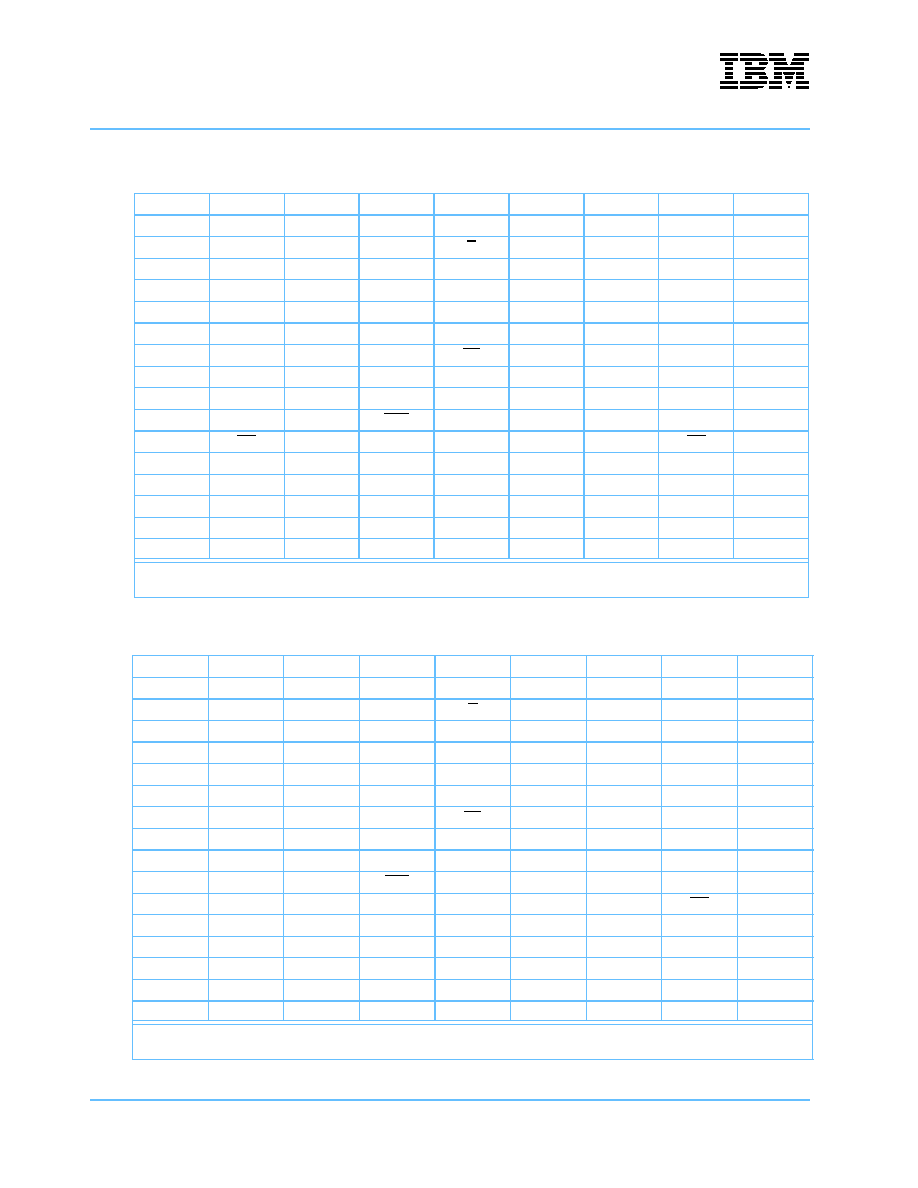
x36 BGA Bump Layout (Top View)
1
2
3
4
5
6
7
8
9
A
V
SS
V
DDQ
SA13
SA11
ZQ
SA10
SA8
V
DDQ
V
SS
B
DQ23
DQ20
SA14
V
SS
B1
V
SS
SA7
DQ15
DQ12
C
V
SS
V
DDQ
SA15
SA12
G
SA9
SA6
V
DDQ
V
SS
D
DQ24
DQ21
SA18
V
SS
V
DD
V
SS
SA5
DQ14
DQ11
E
V
SS
V
DDQ
V
SS
V
DD
V
REF
V
DD
V
SS
V
DDQ
V
SS
F
DQ25
CQ
DQ18
V
DD
V
DD
V
DD
DQ17
CQ
DQ10
G
V
SS
V
DDQ
V
SS
V
SS
CK
V
SS
V
SS
V
DDQ
V
SS
H
DQ26
DQ22
DQ19
V
DD
CK
V
DD
DQ16
DQ13
DQ9
J
V
SS
V
DDQ
V
SS
V
DD
V
DD
V
DD
V
SS
V
DDQ
V
SS
K
DQ27
DQ31
DQ34
V
SS
B2
V
SS
DQ1
DQ4
DQ8
L
V
SS
V
DDQ
V
SS
LBO
B3
MODE
1
V
SS
V
DDQ
V
SS
M
DQ28
CQ
DQ35
V
DD
V
DD
V
DD
DQ0
CQ
DQ7
N
V
SS
V
DDQ
V
SS
V
DD
V
REF
V
DD
V
SS
V
DDQ
V
SS
P
DQ29
DQ32
NC
V
SS
V
DD
V
SS
SA4
DQ3
DQ6
R
V
SS
V
DDQ
V
DD
SA17
SA1
SA2
V
DD
V
DDQ
V
SS
T
DQ30
DQ33
SA16
V
SS
SA0
V
SS
SA3
DQ2
DQ5
U
V
SS
V
DDQ
TMS
TDI
TCK
TDO
NC
2
V
DDQ
V
SS
1. Connect the Mode pin to V
SS
. The Mode pin has a very small pull down, less than 5
�A current at V
DD
input.
2. ESD protection diodes reside on this NC bump.
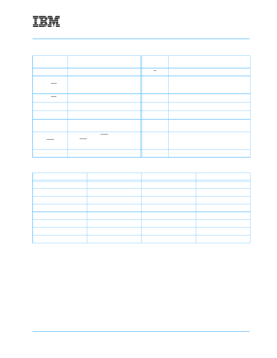
x18 BGA Bump Layout (Top View)
1
2
3
4
5
6
7
8
9
A
V
SS
V
DDQ
SA13
SA11
ZQ
SA10
SA8
V
DDQ
V
SS
B
NC
DQ10
SA14
V
SS
B1
V
SS
SA7
NC
DQ5
C
V
SS
V
DDQ
SA15
SA12
G
SA9
SA6
V
DDQ
V
SS
D
DQ11
NC
SA18
V
SS
V
DD
V
SS
SA5
DQ7
NC
E
V
SS
V
DDQ
V
SS
V
DD
V
REF
V
DD
V
SS
V
DDQ
V
SS
F
NC
CQ
NC
V
DD
V
DD
V
DD
DQ8
NC
DQ4
G
V
SS
V
DDQ
V
SS
V
SS
CK
V
SS
V
SS
V
DDQ
V
SS
H
DQ12
NC
DQ9
V
DD
CK
V
DD
NC
DQ6
NC
J
V
SS
V
DDQ
V
SS
V
DD
V
DD
V
DD
V
SS
V
DDQ
V
SS
K
NC
DQ15
NC
V
SS
B2
V
SS
DQ0
NC
DQ3
L
V
SS
V
DDQ
V
SS
LBO
B3
MODE
1
V
SS
V
DDQ
V
SS
M
DQ13
NC
DQ17
V
DD
V
DD
V
DD
NC
CQ
NC
N
V
SS
V
DDQ
V
SS
V
DD
V
REF
V
DD
V
SS
V
DDQ
V
SS
P
NC
DQ16
SA19
V
SS
V
DD
V
SS
SA4
NC
DQ2
R
V
SS
V
DDQ
V
DD
SA17
SA1
SA2
V
DD
V
DDQ
V
SS
T
DQ14
NC
SA16
V
SS
SA0
V
SS
SA3
DQ1
NC
U
V
SS
V
DDQ
TMS
TDI
TCK
TDO
NC
2
V
DDQ
V
SS
1. Connect the Mode pin to V
SS
. The Mode pin has a very small pull down, less than 5
�A current at V
DD
input.
2. ESD protection diodes reside on this NC bump.
IBM043616CBLBC
IBM041816CBLBC
16Mb (512K x 36 & 1M x 18) SRAM
CBLBCds.fm.00
June 3, 2002
Page 3 of 25
Pin Description
SA0�SA19
Address Input (SA0�SA1 burst-control start-
ing addresses)
TDO
IEEE
1149.1 Test Output (LVTTL level)
DQ0�DQ35 Data
I/O
G
Asynchronous Output Enable
CQ, CQ
Differential Echo Clocks
MODE
Mode Pin. Connect to V
SS
. A waiver to float Mode
may be obtained; contact your field applications
engineer (FAE).
CK, CK
Differential Input Register Clocks
V
REF
HSTL Input Reference Voltage
B1
B1 = 0 initiates a Load operation
V
DD
Power Supply (2.5V)
B2
B2 = 0 initiates a Write operation
V
SS
Ground
B3
B3 = 0 Double Data Rate,
B3 = 1 Single Data Rate
V
DDQ
Output Power Supply
LBO
Linear Burst Order (LBO = 1, interleave
mode; LBO = 0, linear mode), (can be tied to
V
DD
or V
SS
)
ZQ
Output Driver Impedance Control
TMS, TDI, TCK
IEEE 1149.1 Test Inputs (LVTTL levels)
NC
No Connect
Ordering Information
Part Number
Organization
Cycle Time (ns)
Package
IBM043616CBLBC-22
512K x 36
2.2
9 x 17 BGA
IBM043616CBLBC-24
512K x 36
2.4
9 x 17 BGA
IBM043616CBLBC-27
512K x 36
2.7
9 x 17 BGA
IBM043616CBLBC-30
512K x 36
3.0
9 x 17 BGA
IBM041816CBLBC-22
1M x 18
2.2
9 x 17 BGA
IBM041816CBLBC-24
1M x 18
2.4
9 x 17 BGA
IBM041816CBLBC-27
1M x 18
2.7
9 x 17 BGA
IBM041816CBLBC-30
1M x 18
3.0
9 x 17 BGA
IBM043616CBLBC
IBM041816CBLBC
16Mb (512K x 36 & 1M x 18) SRAM
Page 4 of 25
CBLBCds.fm.00
June 3, 2002
Block Diagram (x36 Double Data Rate Mode)
256K x 72
Buffer
Write
Decode
0
2:1
Mu
x
DQ0-DQ35
Read Add
Reg
C
o
mpare
CK,
CK
B1-B3
SA0-SA18
Array
G
1
0
1
Buffer
Write
0
1
0
1
REG
Output
Output
REG
0
1
36
36
36
36
36
36
36
36
REG
Output
Output
REG
0
1
4
4
CQa,CQa
CQb,CQb
0
1
0
1
E
E
VDD
VSS
E
Write
Add Reg
E
Burst
Logic
A2-A18
A0,A1
A0',A1'
A0'
A0'
A0'
A0'
Control
Logic
Load
Write
Output Enable
E
Advance
Match
36
36
IBM043616CBLBC
IBM041816CBLBC
16Mb (512K x 36 & 1M x 18) SRAM
CBLBCds.fm.00
June 3, 2002
Page 5 of 25
SRAM Features
Double Data Rate (DDR) and Single Data Rate (SDR) Modes
The timing diagram on page 6 shows input and output data placements for both DDR and SDR modes. In
DDR read mode, two sets of data-outs are generated from the second rising and falling edges of the CK
clock, assuming the first rising edge of the CK clock samples the base address. The first of the two data-out
sets (DOUT-A) is generated from the sampled base address (Base-A). The second data-out set (DOUT-A') is
generated from the next burst-order address, according to the burst-order definition. Similarly, a DDR write
requires data-in placement on the second rising and falling CK edges. In SDR read mode, only one set of
data-outs is generated from the second rising CK edge. In SDR write mode, one set of data-ins is sampled on
the second rising CK edge. The user may switch from DDR to SDR mode (or vice-versa) during any LOAD
(B1 = 0) operation.
Late Write
The late-write function allows write data to be registered one cycle after addresses and controls. This feature
eliminates one of two bus-turnaround cycles normally required when going from a read to a write operation.
Late write is accomplished by buffering write addresses and data. The SRAM array update occurs during the
third write cycle. Read-cycle addresses are monitored to determine if read data is to be supplied from the
SRAM array or the write buffer. Full data coherency is maintained for both DDR and SDR operations. As a
result, NOP (write buffer flush) operations are not required going from write cycles to read cycles.
Echo Clocks
Echo clocks CQ and CQ are generated from rising and falling edges of the CK clock, with access times repre-
sentative of the data-outs. Echo clocks keep running during write and NOP operations. Echo-clock operation
is identical for both double-data-rate and single-data-rate operations. The close tracking of echo clocks and
data-out timings allows the echo clocks to be used as capture clocks for the data-outs by the receiving
device.