
crlL3325.03
08/06/2001
©IBM Corporation. All rights reserved.
Use is further subject to the provisions at the end of this document.
Page 1 of 24
IBM0418A4ANLAB
IBM0418A8ANLAB
IBM0436A8ANLAB
IBM0436A4ANLAB
Preliminary
8Mb (256Kx36 & 512Kx18) and 4Mb (128Kx36 & 256Kx18) SRAM
Features
∑ 8Mb: 256K x 36 or 512K x 18 organizations
4Mb: 128K x 36 or 256K x 18 organizations
∑ 0.25
µ CMOS technology
∑ Synchronous Register-Latch Mode of Operation
with Self-Timed Late Write
∑ Single Differential PECL Clock
∑ +3.3V Power Supply, Ground, 2.5V V
DDQ
∑ 2.5V LVTTL Input and Output levels
∑ Registered Addresses, Write Enables, Synchro-
nous Select, and Data Ins
∑ Latched Outputs
∑ Common I/O
∑ 30
Drivers
∑ Asynchronous Output Enable and Power Down
Inputs
∑ Boundary Scan using limited set of JTAG
1149.1 functions
∑ Byte Write Capability & Global Write Enable
∑ 7 x 17 Bump Ball Grid Array Package with
SRAM JEDEC Standard Pinout and Boundary
SCAN Order
Description
IBM0436A4ANLAB, IBM0436A8ANLAB,
IBM0418A4ANLAB, and IBM0418A8ANLAB are
4Mb and 8Mb Synchronous Register-Latch Mode,
high-performance CMOS Static Random Access
Memories (SRAMs). These SRAMs are versatile,
have a wide input/output (I/O) interface, and can
achieve cycle times as short as 4.5ns. Differential K
clocks are used to initiate the read/write operation;
all internal operations are self-timed. At the rising
edge of the K clock, all address, write-enables, sync
select, and data input signals are registered inter-
nally. Data outputs are updated from output regis-
ters off the falling edge of the K clock. An internal
write buffer allows write data to follow one cycle
after addresses and controls. The device is oper-
ated with a single +3.3V power supply and is com-
patible with 2.5V LVTTL I/O interfaces.
.

IBM0418A4ANLAB IBM0418A8ANLAB
IBM0436A8ANLAB IBM0436A4ANLAB
8Mb (256Kx36 & 512Kx18) and 4Mb (128Kx36 & 256Kx18) SRAM
Preliminary
©IBM Corporation. All rights reserved.
Use is further subject to the provisions at the end of this document.
Page 2 of 24
crlL3325.03
08/06/2001
x36 BGA Pinout
(Top View)
1
2
3
4
5
6
7
A
V
DDQ
SA
SA
NC
SA
SA
V
DDQ
B
NC
NC
SA
NC
SA
NC,SA(8Mb)
NC
C
NC
SA
SA
V
DD
SA
SA
NC
D
DQ19
DQ18
V
SS
NC
V
SS
DQ9
DQ10
E
DQ22
DQ20
V
SS
SS
V
SS
DQ11
DQb13
F
V
DDQ
DQ21
V
SS
G
V
SS
DQ12
V
DDQ
G
DQ24
DQ23
SBWc
NC
SBWb
DQ14
DQb15
H
DQ25
DQ26
V
SS
NC
V
SS
DQ17
DQb16
J
V
DDQ
V
DD
NC
V
DD
NC
V
DD
V
DDQ
K
DQ34
DQ35
V
SS
K
V
SS
DQ8
DQ7
L
DQ33
DQ32
SBWd
K
SBWa
DQ5
DQ6
M
V
DDQ
DQ30
V
SS
SW
V
SS
DQ3
V
DDQ
N
DQ31
DQ29
V
SS
SA
V
SS
DQ2
DQ4
P
DQ28
DQ27
V
SS
SA
V
SS
DQ0
DQ1
R
NC
SA
M1*
V
DD
M2*
SA
NC
T
NC
NC
SA
SA
SA
NC
ZZ
U
V
DDQ
TMS
TDI
TCK
TDO
NC
V
DDQ
* M1 and M2 are clock mode pins. For this application, M1 and M2 need to connect to V
DD
and V
SS
respectively.
x18 BGA Pinout
(Top View)
1
2
3
4
5
6
7
A
V
DDQ
SA
SA
NC
SA
SA
V
DDQ
B
NC
NC
SA
NC
SA
NC,SA(8Mb)
NC
C
NC
SA
SA
V
DD
SA
SA
NC
D
DQ14
NC
V
SS
NC
V
SS
DQ0
NC
E
NC
DQ15
V
SS
SS
V
SS
NC
DQ1
F
V
DDQ
NC
V
SS
G
V
SS
DQ2
V
DDQ
G
NC
DQ16
SBWb
NC
NC
NC
DQ3
H
DQ17
NC
V
SS
NC
V
SS
DQ4
NC
J
V
DDQ
V
DD
NC
V
DD
NC
V
DD
V
DDQ
K
NC
DQ13
V
SS
K
V
SS
NC
DQ8
L
DQ12
NC
NC
K
SBWa
DQ7
NC
M
V
DDQ
DQ10
V
SS
SW
V
SS
NC
V
DDQ
N
DQ11
NC
V
SS
SA
V
SS
DQ6
NC
P
NC
DQ9
V
SS
SA
V
SS
NC
DQ5
R
NC
SA
M1
V
DD
M2
SA
NC
T
NC
SA
SA
NC
SA
SA
ZZ
U
V
DDQ
TMS
TDI
TCK
TDO
NC
V
DDQ
* M1 and M2 are clock mode pins. For this application, M1 and M2 need to connect to V
DD
and V
SS
respectively.

IBM0418A4ANLAB IBM0418A8ANLAB
IBM0436A8ANLAB IBM0436A4ANLAB
Preliminary
8Mb (256Kx36 & 512Kx18) and 4Mb (128Kx36 & 256Kx18) SRAM
crlL3325.03
08/06/2001
©IBM Corporation. All rights reserved.
Use is further subject to the provisions at the end of this document.
Page 3 of 24
Pin Description
SA0-SA18
Address Input
SA0-SA18 for 512K x 18
SA0-SA17 for 256K x 36
SA0-SA17 for 256K x 18
SA0-SA16 for 128K x 36
TDO
IEEE 1149.1 Test Output (LVTTL level)
DQ0-DQ35
Data I/O
DQ0-DQ17 for 512K x 18
DQ0-DQ35 for 256K x 36
G
Asynchronous Output Enable
K, K
Differential Input Register Clocks
SS
Synchronous Select
SW
Write Enable, Global
M1, M2
Clock Mode Inputs. Selects Single or Dual Clock
Operation.
SBWa
Write Enable, Byte a (DQ0-DQ8)
V
DD
Power Supply (+3.3V)
SBWb
Write Enable, Byte b (DQ9-DQ17)
V
SS
Ground
SBWc
Write Enable, Byte c (DQ18-DQ26)
V
DDQ
Output Power Supply
SBWd
Write Enable, Byte d (DQ27-DQ35)
ZZ
Synchronous Sleep Mode
TMS, TDI, TCK
IEEE
Æ
1149.1 Test Inputs (LVTTL levels)
NC
No Connect
Ordering Information
Part Number
Organization
Speed
Leads
IBM0436A8ANLAB - 4H
256K x 36
4.5ns Access / 4.5ns Cycle
7 x 17 BGA
IBM0436A8ANLAB - 5
256K x 36
5.0ns Access / 5.0ns Cycle
7 x 17 BGA
IBM0436A8ANLAB - 5H
256K x 36
5.5ns Access / 5.5ns Cycle
7 x 17 BGA
IBM0436A4ANLAB - 4H
128K x 36
4.5ns Access / 4.5ns Cycle
7 x 17 BGA
IBM0436A4ANLAB - 5
128K x 36
5.0ns Access / 5.0ns Cycle
7 x 17 BGA
IBM0436A4ANLAB - 5H
128K x 36
5.5ns Access / 5.5ns Cycle
7 x 17 BGA
IBM0418A4ANLAB - 4H
256K x 18
4.5ns Access / 4.5ns Cycle
7 x 17 BGA
IBM0418A4ANLAB - 5
256K x 18
5.0ns Access / 5.0ns Cycle
7 x 17 BGA
IBM0418A4ANLAB - 5H
256K x 18
5.5ns Access / 5.5ns Cycle
7 x 17 BGA
IBM0418A8ANLAB -4H
512K x 18
4.5ns Access / 4.5ns Cycle
7 x 17 BGA
IBM0418A8ANLAB -5
512K x 18
5.0ns Access / 5.0ns Cycle
7 x 17 BGA
IBM0418A8ANLAB -5H
512K x 18
5.5ns Access / 5.5ns Cycle
7 x 17 BGA
IBM0418A4ANLAB IBM0418A8ANLAB
IBM0436A8ANLAB IBM0436A4ANLAB
8Mb (256Kx36 & 512Kx18) and 4Mb (128Kx36 & 256Kx18) SRAM
Preliminary
©IBM Corporation. All rights reserved.
Use is further subject to the provisions at the end of this document.
Page 4 of 24
crlL3325.03
08/06/2001
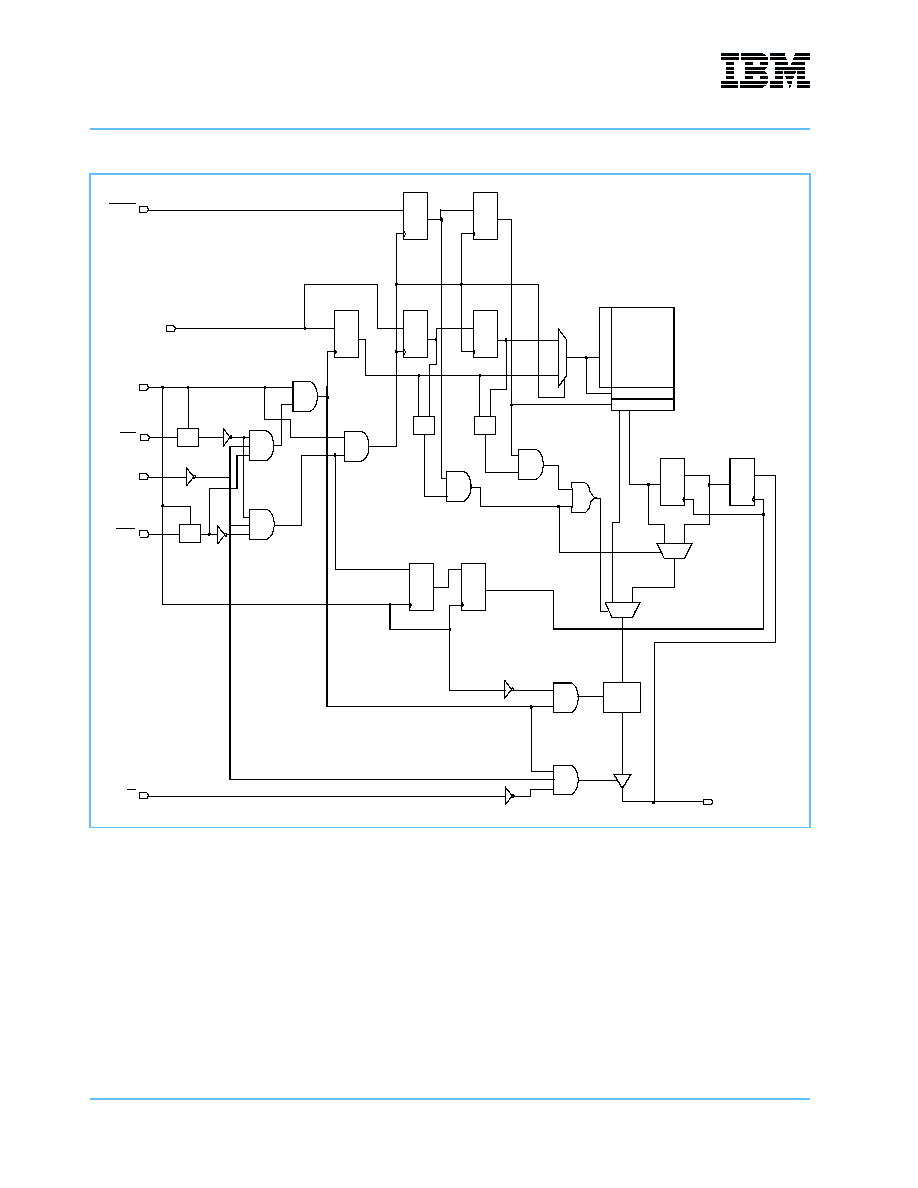
Block Diagram
SBW
Ro
w De
co
d
e
Col Decode
Read/Wr Amp
DOC_Array0
SA0-SA18
K
ZZ
G
SW
SS
DQ0-DQ35
REG
REG
SB
W
2:
1
M
U
X
DOC_MUX0
WR
I
T
E
1
A
DD REG
WRI
T
E
0
A
DD REG
RE
AD
A
DD REG
RE
AD
WR
I
T
E
MA
TC
H
M
A
T
CH1
LATCH
LATCH0
WR_
B
UF
1
WR_
B
UF
0
2:1 MUX
DOC_MUX1
2:1 MUX
DOC_MUX2
SB
W0
SW0
SW1
REG
REG
DOC_
DOUT0

IBM0418A4ANLAB IBM0418A8ANLAB
IBM0436A8ANLAB IBM0436A4ANLAB
Preliminary
8Mb (256Kx36 & 512Kx18) and 4Mb (128Kx36 & 256Kx18) SRAM
crlL3325.03
08/06/2001
©IBM Corporation. All rights reserved.
Use is further subject to the provisions at the end of this document.
Page 5 of 24
SRAM Features
Late Write
The Late Write function allows for write data to be registered one cycle after addresses and controls. This fea-
ture eliminates one bus-turnaround cycle, necessary when going from a read to a write operation. Late write
is accomplished by buffering write addresses and data so that the write operation occurs during the next write
cycle. When a read cycle occurs after a write cycle, the address and write data information are stored tempo-
rarily in holding registers. During the first write cycle preceded by a read cycle, the SRAM array is updated
with address and data from the holding registers. Read cycle addresses are monitored to determine if read
data is to be supplied from the SRAM array or the write buffer. The bypassing of the SRAM array occurs on a
byte-by-byte basis. When only one byte is written during a write cycle, read data from the last written address
has new byte data from the write buffer and remaining bytes from the SRAM array.
Mode Control
Mode control pins M1 and M2 are used to select four different JEDEC-standard read protocols. This SRAM
supports single clock, register latch operation (M1 = V
DD
, M2 = V
SS
). This datasheet describes single clock
register latch functionality only. Mode control inputs must be set at power up and must not change during
SRAM operation. This SRAM is tested only in the register-latch mode.
Sleep Mode
The sleep mode is enabled by switching the synchronous signal ZZ High. When the SRAM is in the sleep
mode, the outputs go to a High-Z state and the SRAM draws standby current. SRAM data is preserved and a
recovery time (t
ZZR
) is required before the SRAM resumes normal operation.
Power-Up Requirements
To ensure the optimum internally regulated supply voltage, the SRAM requires 4
µs of power-up time after
V
DD
reaches its operating range.
Power-Up and Power-Down Sequencing
The power supplies must be powered up in the following order: V
DD
, V
DDQ
, and Inputs. The power-down
sequence must be in the reverse order. V
DDQ
may not exceed V
DD
by more than 0.6V. No special tracking
between power supplies is required.