 | –≠–ª–µ–∫—Ç—Ä–æ–Ω–Ω—ã–π –∫–æ–º–ø–æ–Ω–µ–Ω—Ç: IBMCPC700 | –°–∫–∞—á–∞—Ç—å:  PDF PDF  ZIP ZIP |

CPC700 Memory Controller and PCI Bridge
CPC700
4/17/01
©IBM Corporation. All rights reserved.
Use is further subject to the provisions at the end of this document.
Page 1 of 22
Features
∑ PowerPC 60x/7xx bus.
∑ 66.66 MHz
∑ 83.33 MHz
∑ Synchronous DRAM interface operates at the
processor bus speed with support for ECC.
∑ PCI Revision 2.1 Compliant Interface.
∑ ROM/SRAM/External peripheral controller.
∑ Interrupt Controller supports interrupts from a
variety of sources.
∑ Programmable Timers.
∑ Two 2-wire, 8-bit, 16550 compatible UARTs.
∑ Two independent IIC interfaces.
∑ Byte swapping supported for bi-endian opera-
tion.
∑ Internal PCI Bus Arbiter for PCI bus speeds up
to 33.33 MHz (may be disabled for use with an
external arbiter).
∑ 32-bit PCI bus operates at frequencies from
25MHz to 66.66 Mhz.
∑ Uses standard type 0 PCI configuration register
map essential to making it appear like a device
but does not preclude it from being a host.
∑ Supports independent primary and secondary
resource management mapping. This feature
enables the CPC700 to effectively isolate local
processing resources from host side memory
and I/O allocations. Through the use of three
independent translation decodes, the PowerPC
operating environment access to PCI is man-
aged solely by the PowerPC.
∑ Dual address capabilities enhance the
CPC700's capabilities by allowing it to manage,
control, or test beyond 4GB limitations.
∑ Support for shared memory is locally mapped to
the processor's ROM or SDRAM through PCI
standard Base Address Registers. Two Memory
I/O BARs are available for requesting host
memory or I/O resources and managing PCI to
PowerPC access.
∑ Provides a special interface enabling the
CPC700 to generate any PCI command, includ-
ing Type 1 configuration cycles.
∑ Fully buffers PCI writes and supports PCI read
pre-fetching from local memory.
∑ Hardware enforces cache coherency.
∑ Implemented in CMOS5SE.
.

CPC700 Memory Controller and PCI Bridge
©IBM Corporation. All rights reserved.
Use is further subject to the provisions at the end of this document.
Page 2 of 22
CPC700
4/17/01
Contents
Section 1. "Description" ....................................................................................................... 3
Section 2. "Electrical Characteristics".................................................................................. 4
Section 3. "Signal Lists"..................................................................................................... 12
Section 4. "Package Information" ...................................................................................... 18
Section 5. "Ordering Information" ...................................................................................... 19

CPC700 Memory Controller and PCI Bridge
CPC700
4/17/01
©IBM Corporation. All rights reserved.
Use is further subject to the provisions at the end of this document.
Page 3 of 22
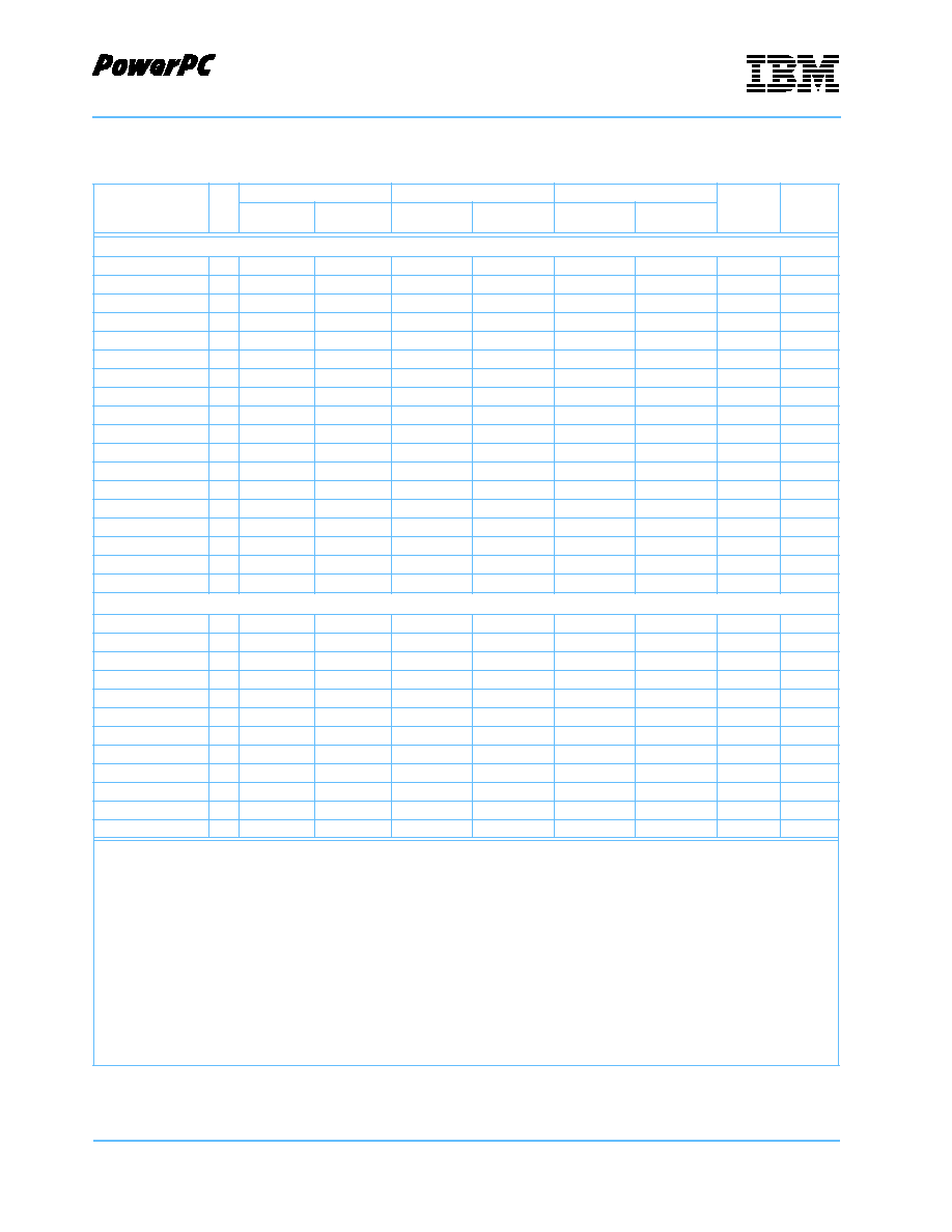
1. Description
The CPC700 contains a bridge from the PowerPC processor to the PCI bus, as well as a high-speed memory
controller, internal peripherals, and control for external ROM and external peripherals. The CPC700 is a gen-
eral purpose solution for interfacing the high performance, superscalar, PowerPC 603e, 740, and 750 families
of RISC microprocessors to a PCI bus and system memory.
CPC700 Embedded Bridge Functional Block Diagram
Processor
SDRAM
ECC
ROM
Peripherals
1/2X
OPB
Bridge
UART
UART
IIC
IIC
GPT
(Timers)
66.66 or 83.33 MHz Processor Local Bus (PLB)
33.33 MHz On Chip P
e
r
ipher
al Bus (OPB)
119
104
2
2
2
2
12
1
9
52
PCI
JTAG
Misc.
UIC
(interrupts)
DCR Bus
System
5
25 to 66.66 MHz PCI Bus
PLL
&
CPC700 ASIC
Interface
Interface
66.66 or 83.33 MHz Processor Bus
8
Parity
or
Arbiter
PCI
Arb
Data
Parity

CPC700 Memory Controller and PCI Bridge
©IBM Corporation. All rights reserved.
Use is further subject to the provisions at the end of this document.
Page 4 of 22
CPC700
4/17/01
2. Electrical Characteristics
Absolute Maximum Ratings
Characteristic
Symbol
Value
Unit
Supply Voltage
V
DD
0 to 3.6
V
PLL0 Supply Voltage
AV
DD0
0 to 3.6
V
PLL1 Supply Voltage
AV
DD1
0 to 3.6
V
Input Voltage
V
IN
0 to 3.6
V
Storage Temperature Range
T
STG
-65 to 150
∞
C
Recommended DC Operating Conditions
Parameter
Symbol
Min
Typ
Max
Unit
Notes
Supply Voltage
V
DD
3.135
3.3
3.465
V
PLL0 Supply Voltage
V
DD
3.135
3.3
3.465
V
PLL1 Supply Voltage
V
DD
3.135
3.3
3.465
V
Input Logic High (3.3V receivers)
V
IH
2.0
V
DD
V
Input Logic High (5.0V receivers)
V
IH
2.0
5.50
V
Input Logic Low
V
IL
0.0
0.8
V
Output Logic High
V
OH
2.4
V
DD
V
Output Logic Low
V
OL
0.0
0.4
V
Input Leakage Current Group 1
I
IL1
--
<1
10
µ
A
2
Input Leakage Current Group 2
I
IL2
--
--
400
µ
A
3
Input Leakage Current Group 3
I
IL3
--
--
-250
µ
A
4
Input Max Allowable Overshoot (3.3V receivers)
V
IMAO3
V
DD
+ 0.6
V
Input Max Allowable Overshoot (5.0V receivers)
V
IMAO5
5.50
V
Input Max Allowable Undershoot (3.3V receivers)
V
IMAU3
-0.60
V
Input Max Allowable Undershoot (5.0V receivers)
V
IMAU5
-0.60
V
Output Max Allowable Overshoot (3.3V receivers)
V
OMAO3
V
DD
+ 0.6
V
Output Max Allowable Overshoot (5.0V receivers)
V
OMAO5
5.50
V
Output Max Allowable Undershoot (3.3V receivers)
V
OMAU3
-0.60
V
Die Junction Temperature
T
J
-40
105
∞
C
1. Refer to the Output Signal Power Ranges Table for power information.
2. Input leakage currents for all inputs except those indicated in Notes 3 and 4.
3. Input leakage current for signals TEST_ENABLE, GBL_N, TSIZ[0], TSIZ[1], TT[0], AND TT[4].
4. Input leakage current for signals TSIZ[2], TT[1], TRST_N, TDI, TMS, TCK, DI1, AND DI2.
5. In addition to any other specification herein, all CPC700 PCI bus I/Os meet or exceed the PCI v2.1 requirements for 3.3V and 5.0V
signalling environments.

CPC700 Memory Controller and PCI Bridge
CPC700
4/17/01
©IBM Corporation. All rights reserved.
Use is further subject to the provisions at the end of this document.
Page 5 of 22
Capacitance
Parameter
Symbol
Min
Max
Unit
Notes
Input Capacitance Group 1
CIN1
--
5
pF
1, 3
Input Capacitance Group 1
CIN2
--
8
pF
2, 3
1. Group 1 includes all signals except those indicated in note 2.
2. Group 2 includes GBL_N, TSIZ[0], TSIZ[1], TT[4], and TT[0].
3. Excludes test signals TEST_ENABLE, DI1_N, DI2_N, RI_N, and JTAG signals.
DC Electrical Characteristics
Parameter
Symbol
Min
Typ
Max
Unit
Notes
Thermal Resistance, Junction to Ambient
15
∞
C/W
1
Thermal Resistance, Junction to Balls
5.9
∞
C/W
1,2
Active Operating Current
I
DD
420 (66.66 MHz)
500 (83.33 MHz)
mA
3
PLL0 Voltage
V
PLL0
3.135
3.3
3.465
V
PLL0 VDD Input current
I
PLL0
14
mA
PLL1 Voltage
V
PLL1
3.135
3.3
3.465
V
PLL1 VDD Input current
I
PLL1
14
mA
1. Under normal operating conditions, the CPC700 does not require a heat sink.
2. Measured from junction to outside corner ball.
3. I
DD
Max is measured at Tc = 105
∞
C, worst case operating conditions for frequency and voltage, and a capacitive load
of 50 pF.
Power
Power
Processor/Memory Frequency
Units
Notes
66.66
83.33
MHz
Typical
1.1
1.2
W
1, 2
Maximum
1.6
1.9
W
2, 3, 4
1. Typical power is measured at VDD=3.3V, 27
∞
C in a system executing typical sequences.
2. Guaranteed by design and characterization and is not tested.
3. Maximum power is measured at VDD=3.6V, 120
∞
C in a system executing worse case sequences with the CPU caches disabled
4. Maximum power at ≠ 40
∞
C can be derived by subtracting 0.05 W from the maximum power number at 120
∞
C.

CPC700 Memory Controller and PCI Bridge
©IBM Corporation. All rights reserved.
Use is further subject to the provisions at the end of this document.
Page 6 of 22
CPC700
4/17/01
Common I/O Specifications for 66.66MHz and 83.33MHz
(Part 1 of 3)
Signal
I/O
Input (ns)
Output (ns)
Output Current (mA)
Clock
Notes
Setup Time
(min)
Hold Time
(min)
Valid Delay
(max)
Hold Time
(min)
I/O H
(max)
I/O L
(min)
PCI Bus Asynchronous Operation
1, 2, 3, 5, 7
AD[0:31]
I/O
1.6
0.0
5.6
1.6
16.8
14
PCI (A)
C/BE_N[0:3]
I/O
2.6
0.0
5.7
1.7
16.8
14
PCI (A)
DEVSEL_N
I/O
2.9
0.0
5.8
1.6
16.8
14
PCI (A)
FRAME_N
I/O
2.9
0.0
5.6
1.8
16.8
14
PCI (A)
IDSEL
I
1.8
0.0
PCI (A)
IRDY_N
I/O
2.8
0.0
5.3
1.7
16.8
14
PCI (A)
PAR
I/O
2.3
0.0
5.3
1.8
16.8
14
PCI (A)
PERR_N
I/O
1.8
0.0
5.4
1.7
16.8
14
PCI (A)
RST_N
O
n/a
n/a
13.4
9
STOP_N
I/O
2.7
0.0
5.8
1.7
16.8
14
PCI (A)
TRDY_N
I/O
2.6
0.0
5.8
1.7
16.8
14
PCI (A)
SERR_N
O
5.8
1.7
16.8
14
PCI (A)
PCI Bus 2:1 Synchronous Operation
1, 2, 4, 5, 7
AD[0:31]
I/O
3.8
0.0
8.7
2.9
16.8
14
PCI (S)
C/BE_N[0:3]
I/O
5.5
0.0
8.6
2.8
16.8
14
PCI (S)
DEVSEL_N
I/O
4.8
0.0
8.4
2.8
16.8
14
PCI (S)
FRAME_N
I/O
5.2
0.0
8.3
2.8
16.8
14
PCI (S)
IDSEL
I
2.5
0.0
16.8
14
PCI (S)
IRDY_N
I/O
5.2
0.0
7.9
2.8
16.8
14
PCI (S)
PAR
I/O
4.7
0.0
8.5
2.8
PCI (S)
PERR_N
I/O
4.1
0.0
8.8
3.1
16.8
14
PCI (S)
STOP_N
I/O
3.6
0.0
8.5
2.9
16.8
14
PCI (S)
TRDY_N
I/O
4.6
0.0
8.5
2.9
16.8
14
PCI (S)
SERR_N
O
8.3
2.3
16.8
14
PCI (S)
1. Timing is guaranteed by design and characterization and is not tested.
2. All I/O timing (CPU, PCI, and other) is specified into a 50pf load. All timings include errors (if any) induced by internal PLLs, given
a clock input with no jitter.
Sys (2X): Timings shown are referenced to the rising edge of the output of PLL0, operating at twice the frequency of the
SYS_CLK input. PLL0 locks to the rising edge of SYS_CLK.
Sys (1X): Timing is referenced to SYS_CLK.
PCI (A): PCI interface in asynchronous mode. Timings are referenced to the PCI_CLK input. Logic is clocked by the output of
PLL1, which repeats PCI_CLK.
PCI (S): PCI interface in synchronous mode. Timings are referenced to the SYS_CLK, which is assumed to be exactly equal
to the PCI clock.
3. Asynchronous PCI timings reflect 66.66 MHz PCI operation. Output timings are specified into a 50pF load.
4. PCI in 2:1 (CPU @ 66.66MHz, PCI @ 33.33 MHz).
5. All PCI timings meet or exceed PCI v2.1 specifications. System designers should design using the PCI timing budgets of the PCI
version 2.1 specifications. Output delays are specified into a 50pF lumped load model.
6. IIC output timing specified into a 250pF load.
7. This is a 5.0V receiver. Other receivers are 3.3V receivers.

CPC700 Memory Controller and PCI Bridge
CPC700
4/17/01
©IBM Corporation. All rights reserved.
Use is further subject to the provisions at the end of this document.
Page 7 of 22
PCI Arbitration
1, 2, 5
GNT0_N/REQ_N
O
8.8
2.7
16.8
14
PCI (A)
Async
Internal
Arbiter
9.3
2.9
16.8
14
PCI (S)
Sync
Internal
Arbiter
5.3
1.7
16.8
14
PCI (A)
Async
External
Arbiter
7.6
2.6
16.8
14
PCI (S)
Sync
External
Arbiter
REQ0_N/GNT_N
I
4.7
0.0
PCI (A)
Async
Internal
Arbiter
4.7
0.0
Sys (S)
Sync
Internal
Arbiter
2.7
0.0
PCI (A)
Async
External
Arbiter
5.1
0.0
PCI (S)
Sync
External
Arbiter
REQ[1:5]_N
I
4.4
0.0
PCI (A)
Async
Internal
Arbiter
4.4
0.0
PCI (S)
Sync
Internal
Arbiter
GNT[1:5]_N
O
8.8
2.7
16.8
14
PCI (A)
Async
Internal
Arbiter
9.3
2.9
16.8
14
PCI (S)
Sync
Internal
Arbiter
Common I/O Specifications for 66.66MHz and 83.33MHz
(Part 2 of 3)
Signal
I/O
Input (ns)
Output (ns)
Output Current (mA)
Clock
Notes
Setup Time
(min)
Hold Time
(min)
Valid Delay
(max)
Hold Time
(min)
I/O H
(max)
I/O L
(min)
1. Timing is guaranteed by design and characterization and is not tested.
2. All I/O timing (CPU, PCI, and other) is specified into a 50pf load. All timings include errors (if any) induced by internal PLLs, given
a clock input with no jitter.
Sys (2X): Timings shown are referenced to the rising edge of the output of PLL0, operating at twice the frequency of the
SYS_CLK input. PLL0 locks to the rising edge of SYS_CLK.
Sys (1X): Timing is referenced to SYS_CLK.
PCI (A): PCI interface in asynchronous mode. Timings are referenced to the PCI_CLK input. Logic is clocked by the output of
PLL1, which repeats PCI_CLK.
PCI (S): PCI interface in synchronous mode. Timings are referenced to the SYS_CLK, which is assumed to be exactly equal
to the PCI clock.
3. Asynchronous PCI timings reflect 66.66 MHz PCI operation. Output timings are specified into a 50pF load.
4. PCI in 2:1 (CPU @ 66.66MHz, PCI @ 33.33 MHz).
5. All PCI timings meet or exceed PCI v2.1 specifications. System designers should design using the PCI timing budgets of the PCI
version 2.1 specifications. Output delays are specified into a 50pF lumped load model.
6. IIC output timing specified into a 250pF load.
7. This is a 5.0V receiver. Other receivers are 3.3V receivers.

CPC700 Memory Controller and PCI Bridge
©IBM Corporation. All rights reserved.
Use is further subject to the provisions at the end of this document.
Page 8 of 22
CPC700
4/17/01
IRQ [0:11], RESET_N, and PCI_66_STRAP are asynchronous inputs that use 5.0V receivers. Timing to the
clock and output characteristics are not specified for these pins.
There is an internal 13K
pull-down resistor connected to pin TEST_ENABLE.
There are internal 13K
pull-down resistors connected to pins GBL_N, TSIZ [0:1], TT [0], and TT [4].
There are internal 20K
pull-up resistors connected to pins TSIZ [2] and TT [1].
ROM Interface
ROM_ALE
O
12.1
4.5
10.2
6.8
Sys (2X)
ROM_OE_N
O
8.1
2.8
19
16
Sys (2X)
ROM_RD_N
O
9.0
3.3
13.4
9
Sys (2X)
7
ROM_READY
I
3.5
1.0
Sys (2X)
ROM_RNW
O
8.6
3.1
13.4
9
Sys (2X)
ROM_WE_N
O
7.8
2.8
19
16
Sys (2X)
ROM_WR_N
O
9.0
3.3
13.4
9
Sys (2X)
IIC Port
IIC_SCL
I/O
3.0
1.0
22.7
4.3
13.4
9
Sys (1X)
6, 7
IIC_SDA
I/O
2.0
1.0
21.6
4.3
13.4
9
Sys (1X)
6, 7
UART Ports
UART_RX
I
2.5
1.0
Sys (1X)
UART_TX
O
11.1
3.9
10.2
6.8
Sys (1X)
Miscellaneous
RESET_OUT_N
O
19
16
Sys (2X)
IRQ_OUT_N
O
10.2
6.8
TDO
O
10.2
6.8
Common I/O Specifications for 66.66MHz and 83.33MHz
(Part 3 of 3)
Signal
I/O
Input (ns)
Output (ns)
Output Current (mA)
Clock
Notes
Setup Time
(min)
Hold Time
(min)
Valid Delay
(max)
Hold Time
(min)
I/O H
(max)
I/O L
(min)
1. Timing is guaranteed by design and characterization and is not tested.
2. All I/O timing (CPU, PCI, and other) is specified into a 50pf load. All timings include errors (if any) induced by internal PLLs, given
a clock input with no jitter.
Sys (2X): Timings shown are referenced to the rising edge of the output of PLL0, operating at twice the frequency of the
SYS_CLK input. PLL0 locks to the rising edge of SYS_CLK.
Sys (1X): Timing is referenced to SYS_CLK.
PCI (A): PCI interface in asynchronous mode. Timings are referenced to the PCI_CLK input. Logic is clocked by the output of
PLL1, which repeats PCI_CLK.
PCI (S): PCI interface in synchronous mode. Timings are referenced to the SYS_CLK, which is assumed to be exactly equal
to the PCI clock.
3. Asynchronous PCI timings reflect 66.66 MHz PCI operation. Output timings are specified into a 50pF load.
4. PCI in 2:1 (CPU @ 66.66MHz, PCI @ 33.33 MHz).
5. All PCI timings meet or exceed PCI v2.1 specifications. System designers should design using the PCI timing budgets of the PCI
version 2.1 specifications. Output delays are specified into a 50pF lumped load model.
6. IIC output timing specified into a 250pF load.
7. This is a 5.0V receiver. Other receivers are 3.3V receivers.

CPC700 Memory Controller and PCI Bridge
CPC700
4/17/01
©IBM Corporation. All rights reserved.
Use is further subject to the provisions at the end of this document.
Page 9 of 22
CPU and Memory Interface I/O Specifications for 66.66 MHz
Signal
I/O
Input (ns)
Output (ns)
Output Current (mA)
Clock
Notes
Setup Time
(min)
Hold Time
(min)
Valid Delay
(max)
Hold Time
(min)
I/O H
(max)
I/O L
(min)
CPU Bus Interface
1, 2
A[0:31]
I/O
3.0
1.0
10.3
3.5
Sys (2X)
AACK_N
O
9.3
3.5
10.2
6.8
Sys (2X)
AP[0:3]
I/O
2.5
1.0
9.4
3.4
16.8
14
Sys (2X)
ARTRY_N
I/O
2.5
1.0
8.5
3.2
10.2
6.8
Sys (2X)
BG_N
O
8.5
3.2
10.2
6.8
Sys (2X)
BR_N
I
3.0
1.0
Sys (2X)
DBG_N
O
9.5
3.5
10.2
6.8
Sys (2X)
DH[0:31]
I/O
3.0
1.0
9.6
3.4
10.2
6.8
Sys (2X)
DL[0:31]
I/O
3.0
1.0
9.8
3.5
10.2
6.8
Sys (2X)
DP[0:7]
I/O
2.5
1.0
6.1
1.8
16.8
14
Sys (2X)
3
GBL_N
O
9.5
3.5
10.2
6.8
Sys (2X)
6
MCP_N
O
10.3
3.9
10.2
6.8
Sys (2X)
4
MCP_REQ
I
2.5
1.0
Sys (2X)
3
TA_N
O
9.1
3.2
10.2
6.8
Sys (2X)
TBST_N
I/O
2.5
1.0
10.1
3.6
10.2
6.8
Sys (2X)
5
TS_N
I/O
3.0
1.0
8.6
2.9
10.2
6.8
Sys (2X)
TSIZ[0:2]
I/O
2.5
1.0
9.8
3.5
10.2
6.8
Sys (2X)
TT[0:4]
I/O
2.5
1.0
9.3
3.5
10.2
6.8
Sys (2X)
Memory Controller Interface
1, 2
BA0
O
11.1
2.8
19
16
Sys (2X)
BA1
O
10.6
2.8
19
16
Sys (2X)
BANK_SEL_N[0:4]
O
8.1
2.8
13.4
9
Sys (2X)
CAS_N
O
6.6
2.4
19
16
Sys (2X)
CKE
O
6.8
2.4
19
16
Sys (2X)
M_DATA[0:63]
I/O
3.0
1.0
7.8
2.8
13.4
9
Sys (2X)
DQM[0]
O
6.9
2.5
19
16
Sys (2X)
ECC[0]
I/O
3.0
1.0
8.0
2.9
13.4
9
Sys (2X)
ECC[1:7]/DQM[1:7]
I/O
3.0
1.0
8.0
2.9
13.4
9
Sys (2X)
MA[0:12]
O
11.1
3.0
19
16
Sys (2X)
RAS_N
O
6.9
2.4
19
16
Sys (2X)
WE_N
O
6.7
2.4
19
16
Sys (2X)
1. Timing is guaranteed by design and characterization and is not tested.
2. All I/O timing (CPU, PCI, and other) is specified into a 50pf load. All timings include errors (if any) induced by internal PLLs, given
a clock input with no jitter.
Sys (2X): Timings shown are referenced to the rising edge of the output of PLL0, operating at twice the frequency of the
SYS_CLK input. PLL0 locks to the rising edge of SYS_CLK.
Sys (1X): Timing is referenced to SYS_CLK.
PCI (A): PCI interface in asynchronous mode. Timings are referenced to the PCI_CLK input. Logic is clocked by the output of
PLL1, which repeats PCI_CLK.
PCI (S): PCI interface in synchronous mode. Timings are referenced to the SYS_CLK, which is assumed to be exactly equal
to the PCI clock...
3. This is a 5.0V receiver. Other receivers are 3.3V receivers
4. This output mimics an open collector gate and requires a pull-up resistor.
5. TBST_N is never driven low. TBST_N is driven high on snoops.
6. GBL_N is not sampled.
CPC700 Memory Controller and PCI Bridge
©IBM Corporation. All rights reserved.
Use is further subject to the provisions at the end of this document.
Page 10 of 22
CPC700
4/17/01
CPU and Memory Interface I/O Specifications for 83.33 MHz
Signal
I/O
Input (ns)
Output (ns)
Output Current (mA)
Clock
Notes
Setup Time
(min)
Hold Time
(min)
Valid Delay
(max)
Hold Time
(min)
I/O H
(max)
I/O L
(min)
CPU Bus Interface
1, 2
A[0:31]
I/O
2.5
1.0
6.6
3.5
Sys (2X)
AACK_N
O
6.5
3.5
10.2
6.8
Sys (2X)
AP[0:3]
I/O
2.5
1.0
6.6
3.4
16.8
14
Sys (2X)
ARTRY_N
I/O
2.5
1.0
6.0
3.2
10.2
6.8
Sys (2X)
BG_N
O
6.0
3.2
10.2
6.8
Sys (2X)
BR_N
I
2.5
1.0
Sys (2X)
DBG_N
O
6.7
3.5
10.2
6.8
Sys (2X)
DH[0:31]
I/O
3.0
1.0
7.1
3.4
10.2
6.8
Sys (2X)
DL[0:31]
I/O
3.0
1.0
7.1
3.5
10.2
6.8
Sys (2X)
DP[0:7]
I/O
2.5
1.0
6.1
1.8
16.8
14
Sys (2X)
3
GBL_N
O
7.2
3.5
10.2
6.8
Sys (2X)
6
MCP_N
O
7.8
3.9
10.2
6.8
Sys (2X)
4
MCP_REQ
I
2.5
1.0
Sys (2X)
3
TA_N
O
6.0
3.2
10.2
6.8
Sys (2X)
TBST_N
I/O
2.5
1.0
7.6
3.6
10.2
6.8
Sys (2X)
5
TS_N
I/O
2.5
1.0
6.0
2.9
10.2
6.8
Sys (2X)
TSIZ[0:2]
I/O
2.5
1.0
6.7
3.5
10.2
6.8
Sys (2X)
TT[0:4]
I/O
2.1
1.0
7.0
3.5
10.2
6.8
Sys (2X)
Memory Controller Interface
1, 2
BA0
O
9.0
2.8
19
16
Sys (2X)
BA1
O
8.5
2.8
19
16
Sys (2X)
BANK_SEL_N[0:4]
O
6.0
2.8
13.4
9
Sys (2X)
CAS_N
O
5.9
2.4
19
16
Sys (2X)
CKE
O
5.8
2.4
19
16
Sys (2X)
M_DATA[0:63]
I/O
2.5
1.0
6.0
2.8
13.4
9
Sys (2X)
DQM[0]
O
5.7
2.5
19
16
Sys (2X)
ECC[0]
I/O
2.5
1.0
6.0
2.9
13.4
9
Sys (2X)
ECC[1:7]/DQM[1:7]
I/O
2.5
1.0
6.0
2.9
13.4
9
Sys (2X)
MA[0:12]
O
8.9
3.0
19
16
Sys (2X)
RAS_N
O
5.8
2.4
19
16
Sys (2X)
WE_N
O
5.7
2.4
19
16
Sys (2X)
1. Timing is guaranteed by design and characterization and is not tested.
2. All I/O timing (CPU, PCI, and other) is specified into a 50pf load. All timings include errors (if any) induced by internal PLLs, given
a clock input with no jitter.
Sys (2X): Timings shown are referenced to the rising edge of the output of PLL0, operating at twice the frequency of the
SYS_CLK input. PLL0 locks to the rising edge of SYS_CLK.
Sys (1X): Timing is referenced to SYS_CLK.
PCI (A): PCI interface in asynchronous mode. Timings are referenced to the PCI_CLK input. Logic is clocked by the output of
PLL1, which repeats PCI_CLK.
PCI (S): PCI interface in synchronous mode. Timings are referenced to the SYS_CLK, which is assumed to be exactly equal
to the PCI clock.
3. This is a 5.0V receiver. Other receivers are 3.3V receivers.
4. This output mimics an open collector gate and requires a pull-up resistor.
5. TBST_N is never driven low. TBST_N is driven high on snoops.
6. GBL_N is not sampled.

CPC700 Memory Controller and PCI Bridge
CPC700
4/17/01
©IBM Corporation. All rights reserved.
Use is further subject to the provisions at the end of this document.
Page 11 of 22
Clock DC Specifications
Signal Name
Minimum Vih
Maximum Vil
Cin
SYS_CLK
2.0V
0.8V
5pf
PCI_CLK
2.0V
0.8V
5pf
CPC700 - 66 Clock AC Specifications
Signal Name
Input
Jitter
Duty Cycle
Fmin
Fmax
Short
Long
Min
Max
Notes
SYS_CLK
30 MHz
33.33MHz
±
150ps
±
250ps
40%
60%
3
PCI_CLK
25 MHz
66.66MHz
±
150ps
±
250ps
40%
60%
1. In the clock tables, 25 MHz represents 1/(40ns), 33.33MHz represents 1/(30ns), 41.66MHz represents 1/(24ns), 66.66MHz repre-
sents 1/(15ns), and 83.33MHz represents 1/(12ns).
2. For information on CPC700 operation with a spread spectrum clock, please contact your IBM technical representative.
CPC700 - 83 Clock AC Specifications
Signal Name
Input
Jitter
Duty Cycle
Fmin
Fmax
Short
Long
Min
Max
Notes
SYS_CLK
30MHz
41.66MHz
±
150ps
±
250ps
40%
60%
3
PCI_CLK
25MHz
66.66MHz
±
150ps
±
250ps
40%
60%
1. In the clock tables, 25MHz represents 1/(40ns), 33.33MHz represents 1/(30ns), 41.66MHz represents 1/(24ns), 66.66MHz repre-
sents 1/(15ns), and 83.33MHz represents 1/(12ns).
2. For information on CPC700 operation with a spread spectrum clock, please contact your IBM technical representative.
3. In previous versions of this data sheet, SYS_CLK Fmin was incorrectly listed as 10 MHz.

CPC700 Memory Controller and PCI Bridge
©IBM Corporation. All rights reserved.
Use is further subject to the provisions at the end of this document.
Page 12 of 22
CPC700
4/17/01
3. Signal Lists
Pin Number List
(Part 1 of 9)
Pin
Signal
A01
NO BALL
A02
ECC7/DQM7
A03
ECC5/DQM5
A04
M_DATA63
A05
M_DATA61
A06
UNUSED
A07
M_DATA59
A08
UNUSED
A09
M_DATA41
A10
UNUSED
A11
M_DATA26
A12
UNUSED
A13
M_DATA22
A14
UNUSED
A15
M_DATA08
A16
M_DATA01
A17
BANK_SEL_N2
A18
BANK_SEL_N1
A19
GND
AA01
AD03
AA02
GND
AA03
VDD
AA04
A02
AA05
A16
AA06
VDD
AA07
DL06
AA08
GND
AA09
DL22
AA10
VDD
AA11
DH08
AA12
GND
AA13
DH13
AA14
VDD
AA15
DP7/GNT5_N
AA16
DH25
AA17
AP3
AA18
GND
AA19
A31
AB01
AD00
AB02
AD01
AB03
A06
AB04
A10
AB05
A24
AB06
DL01
AB07
DL08
AB08
DL18
AB09
DL11
AB10
DH05
AB11
DH06
AB12
DH19
AB13
DH12
AB14
DH17
AB15
DH21
AB16
DH29
AB17
A27
AB18
DL25
AB19
AP0
AC01
A00
AC02
A08
AC03
A04
AC04
VDD
AC05
DL04
AC06
DL07
AC07
DH02
AC08
VDD
AC09
DL17
AC10
DP1/REQ3_N
AC11
DH07
AC12
VDD
AC13
RI
AC14
DH18
AC15
DH24
AC16
VDD
AC17
DL29
AC18
DL23
AC19
DL28
AD01
A14
AD02
A12
AD03
A20
AD04
A28
AD05
DP3/REQ5_N
AD06
GND
AD07
DH03
AD08
DL10
AD09
DH00
AD10
GND
AD11
DH14
AD12
DP2/REQ4_N
AD13
DP5/GNT3_N
AD14
GND
AD15
DH26
AD16
DH28
AD17
DL31
AD18
DL24
AD19
DL27
AE01
GND
AE02
A22
AE03
A26
AE04
A30
AE05
DL02
AE06
UNUSED
AE07
DH09
AE08
UNUSED
AE09
DH10
AE10
UNUSED
AE11
DH11
Pin Number List
(Part 2 of 9)
Pin
Signal
AE12
UNUSED
AE13
DH27
AE14
UNUSED
AE15
DH30
AE16
DH31
AE17
DL30
AE18
DL26
AE19
GND
B01
UART0_TX
B02
ECC6/DQM6
B03
ECC4/DQM4
B04
M_DATA62
B05
M_DATA60
B06
GND
B07
M_DATA47
B08
M_DATA42
B09
M_DATA39
B10
GND
B11
M_DATA25
B12
M_DATA21
B13
M_DATA23
B14
GND
B15
M_DATA00
B16
M_DATA02
B17
BANK_SEL_N3
B18
BANK_SEL_N0
B19
CKE
C01
UART0_RX
C02
UART1_TX
C03
ECC1/DQM1
C04
VDD
C05
M_DATA54
C06
M_DATA55
C07
M_DATA45
C08
VDD
C09
M_DATA35
C10
VDD
C11
M_DATA27
C12
VDD
C13
M_DATA13
C14
M_DATA09
C15
M_DATA03
C16
VDD
C17
BANK_SEL_N4
C18
CAS_N
C19
RAS_N
D01
IRQ0
D02
UART1_RX
D03
ECC0
D04
ECC2/DQM2
D05
M_DATA58
D06
M_DATA46
D07
M_DATA44
Pin Number List
(Part 3 of 9)
Pin
Signal

CPC700 Memory Controller and PCI Bridge
CPC700
4/17/01
©IBM Corporation. All rights reserved.
Use is further subject to the provisions at the end of this document.
Page 13 of 22
D08
M_DATA40
D09
M_DATA36
D10
M_DATA31
D11
M_DATA17
D12
M_DATA19
D13
M_DATA12
D14
M_DATA11
D15
M_DATA04
D16
UNUSED
D17
MA11
D18
WE_N
D19
DQM0
E01
IRQ02
E02
GND
E03
IIC0_SCL
E04
ECC3/DQM3
E05
M_DATA57
E06
VDD
E07
M_DATA43
E08
GND
E09
M_DATA34
E10
VDD
E11
M_DATA18
E12
GND
E13
M_DATA15
E14
VDD
E15
M_DATA05
E16
M_DATA06
E17
MA06
E18
GND
E19
MA09
F01
UNUSED
F02
IIC1_SCL
F03
IIC1_SDA
F04
IIC0_SDA
F05
M_DATA56
F06
UNUSED
F07
GND
F08
M_DATA32
F09
M_DATA33
F10
M_DATA30
F11
M_DATA24
F12
M_DATA20
F13
M_DATA14
F14
M_DATA10
F15
M_DATA07
F16
MA03
F17
MA05
F18
MA07
F19
UNUSED
G01
IRQ05
G02
GND
G03
IRQ01
G04
VDD
G05
IRQ04
Pin Number List
(Part 4 of 9)
Pin
Signal
G06
GND
G07
UNUSED
G08
VDD
G09
UNUSED
G10
GND
G11
UNUSED
G12
VDD
G13
UNUSED
G14
GND
G15
ROM_RD_N
G16
VDD
G17
MA04
G18
MA10/AP
G19
MA08
H01
PCIPLL_VDDA
H02
IRQ06
H03
PCI_CLK
H04
VDD
H05
IRQ03
H06
UNUSED
H07
UNUSED
H08
UNUSED
H09
M_DATA53
H10
M_DATA38
H11
M_DATA16
H12
UNUSED
H13
UNUSED
H14
ROM_ALE
H15
UNUSED
H16
MA02
H17
MA01
H18
MA00
H19
MA12
J01
UNUSED
J02
VDD
J03
IRQ08
J04
GND
J05
IRQ10
J06
VDD
J07
UNUSED
J08
GND
J09
M_DATA52
J10
VDD
J11
M_DATA29
J12
GND
J13
UNUSED
J14
VDD
J15
UNUSED
J16
GND
J17
BA1
J18
VDD
J19
UNUSED
K01
RST_N
K02
IRQ11
K03
TMS
Pin Number List
(Part 5 of 9)
Pin
Signal
K04
REQ0_N/GNT_N
K05
GNT1_N
K06
IRQ09
K07
UNUSED
K08
M_DATA49
K09
M_DATA51
K10
M_DATA37
K11
M_DATA28
K12
ROM_OE_N
K13
UNUSED
K14
UNUSED
K15
ROM_WR_N
K16
ROM_RNW
K17
TDO
K18
BA0
K19
SYS_RESET_N
L01
UNUSED
L02
DEVSEL_N
L03
PAR
L04
VDD
L05
IRQ07
L06
GND
L07
IDSEL
L08
VDD
L09
M_DATA50
L10
GND
L11
GND
L12
VDD
L13
ROM_READY
L14
GND
L15
ROM_WE_N
L16
VDD
L17
RESET_OUT_N
L18
PCI_66_STRAP
L19
UNUSED
M01
AD28
M02
AD20
M03
REQ1_N
M04
AD30
M05
AD31
M06
SERR_N
M07
GNT0_N/REQ_N
M08
PERR_N
M09
VDD
M10
M_DATA48
M11
VDD
M12
DBG_N
M13
TA_N
M14
AACK_N
M15
TEST_ENABLE
M16
MCP_N
M17
SYS_CLK
M18
GND
M19
SYSPLL_VDDA
N01
AD19
Pin Number List
(Part 6 of 9)
Pin
Signal

CPC700 Memory Controller and PCI Bridge
©IBM Corporation. All rights reserved.
Use is further subject to the provisions at the end of this document.
Page 14 of 22
CPC700
4/17/01
N02
VDD
N03
AD27
N04
GND
N05
AD26
N06
VDD
N07
FRAME_N
N08
GND
N09
AD29
N10
GND
N11
TSIZ2
N12
GND
N13
TSIZ1
N14
VDD
N15
BR_N
N16
GND
N17
GBL_N
N18
VDD
N19
MCP_REQ
P01
C/BE_N0
P02
AD21
P03
TCK
P04
IRDY_N
P05
AD23
P06
TRDY_N
P07
AD24
P08
AD11
P09
VDD
P10
AD25
P11
VDD
P12
ARTRY_N
P13
IRQ_OUT_N
P14
TS_N
P15
TT3
P16
TSIZ0
P17
TDI
P18
VDD
P19
TRST_N
R01
AD15
R02
AD17
R03
AD18
R04
VDD
R05
AD14
R06
GND
R07
UNUSED
R08
VDD
R09
DL03
R10
GND
R11
DL12
R12
VDD
R13
A23
R14
GND
R15
TT0
R16
VDD
R17
BG_N
R18
TT4
Pin Number List
(Part 7 of 9)
Pin
Signal
R19
TBST_N
T01
AD13
T02
C/BE_N1
T03
AD16
T04
STOP_N
T05
AD12
T06
UNUSED
T07
UNUSED
T08
C/BE_N3
T09
DL14
T10
DL13
T11
DL09
T12
DL19
T13
UNUSED
T14
A01
T15
A21
T16
AP1
T17
A07
T18
TT1
T19
TT2
U01
UNUSED
U02
VDD
U03
AD22
U04
GND
U05
UNUSED
U06
VDD
U07
UNUSED
U08
GND
U09
UNUSED
U10
VDD
U11
DL05
U12
GND
U13
UNUSED
U14
VDD
U15
UNUSED
U16
GND
U17
A03
U18
VDD
U19
UNUSED
V01
DI1_N
V02
AD09
V03
DI2_N
V04
AD10
V05
C/BE_N2
V06
UNUSED
V07
UNUSED
V08
UNUSED
V09
DL16
V10
DH04
V11
DL00
V12
DH16
V13
UNUSED
V14
UNUSED
V15
A09
V16
AP2
Pin Number List
(Part 8 of 9)
Pin
Signal
V17
A11
V18
A13
V19
A05
W01
AD08
W02
AD07
W03
AD06
W04
VDD
W05
UNUSED
W06
GND
W07
UNUSED
W08
VDD
W09
DP0/REQ2_N
W10
GND
W11
DH15
W12
VDD
W13
UNUSED
W14
GND
W15
UNUSED
W16
VDD
W17
A15
W18
A25
W19
A17
Y01
UNUSED
Y02
AD04
Y03
AD05
Y04
AD02
Y05
A18
Y06
UNUSED
Y07
DP6/GNT4_N
Y08
DH01
Y09
DL15
Y10
DL20
Y11
DL21
Y12
DH20
Y13
DH23
Y14
UNUSED
Y15
DH22
Y16
DP4/GNT2_N
Y17
A19
Y18
A29
Y19
UNUSED
Pin Number List
(Part 9 of 9)
Pin
Signal
CPC700 Memory Controller and PCI Bridge
CPC700
4/17/01
©IBM Corporation. All rights reserved.
Use is further subject to the provisions at the end of this document.
Page 15 of 22
Signal Name List
(Part 1 of 9)
Pin
Signal
AC01
A00
T14
A01
AA04
A02
U17
A03
AC03
A04
V19
A05
AB03
A06
T17
A07
AC02
A08
V15
A09
AB04
A10
V17
A11
AD02
A12
V18
A13
AD01
A14
W17
A15
AA05
A16
W19
A17
Y05
A18
Y17
A19
AD03
A20
T15
A21
AE02
A22
R13
A23
AB05
A24
W18
A25
AE03
A26
AB17
A27
AD04
A28
Y18
A29
AE04
A30
AA19
A31
M14
AACK_N
AB01
AD00
AB02
AD01
Y04
AD02
AA01
AD03
Y02
AD04
Y03
AD05
W03
AD06
W02
AD07
W01
AD08
V02
AD09
V04
AD10
P08
AD11
T05
AD12
T01
AD13
R05
AD14
R01
AD15
T03
AD16
R02
AD17
R03
AD18
N01
AD19
M02
AD20
P02
AD21
U03
AD22
P05
AD23
P07
AD24
P10
AD25
N05
AD26
N03
AD27
M01
AD28
N09
AD29
M04
AD30
M05
AD31
AB19
AP0
T16
AP1
V16
AP2
AA17
AP3
P12
ARTRY_N
K18
BA0
J17
BA1
B18
BANK_SEL_N0
A18
BANK_SEL_N1
A17
BANK_SEL_N2
B17
BANK_SEL_N3
C17
BANK_SEL_N4
R17
BG_N
N15
BR_N
P01
C/BE_N0
T02
C/BE_N1
V05
C/BE_N2
T08
C/BE_N3
C18
CAS_N
B19
CKE
M12
DBG_N
L02
DEVSEL_N
AD09
DH00
Y08
DH01
AC07
DH02
AD07
DH03
V10
DH04
AB10
DH05
AB11
DH06
AC11
DH07
AA11
DH08
AE07
DH09
AE09
DH10
AE11
DH11
AB13
DH12
AA13
DH13
AD11
DH14
W11
DH15
V12
DH16
AB14
DH17
AC14
DH18
AB12
DH19
Y12
DH20
AB15
DH21
Y15
DH22
Signal Name List
(Part 2 of 9)
Pin
Signal
Y13
DH23
AC15
DH24
AA16
DH25
AD15
DH26
AE13
DH27
AD16
DH28
AB16
DH29
AE15
DH30
AE16
DH31
V01
DI1_N
V03
DI2_N
V11
DL00
AB06
DL01
AE05
DL02
R09
DL03
AC05
DL04
U11
DL05
AA07
DL06
AC06
DL07
AB07
DL08
T11
DL09
AD08
DL10
AB09
DL11
R11
DL12
T10
DL13
T09
DL14
Y09
DL15
V09
DL16
AC09
DL17
AB08
DL18
T12
DL19
Y10
DL20
Y11
DL21
AA09
DL22
AC18
DL23
AD18
DL24
AB18
DL25
AE18
DL26
AD19
DL27
AC19
DL28
AC17
DL29
AE17
DL30
AD17
DL31
W09
DP0/REQ2_N
AC10
DP1/REQ3_N
AD12
DP2/REQ4_N
AD05
DP3/REQ5_N
Y16
DP4/GNT4_N
AD13
DP5/GNT3_N
Y07
DP6/GNT4_N
AA15
DP7/GNT5_N
D19
DQM0
D03
ECC0
C03
ECC1/DQM1
D04
ECC2/DQM2
Signal Name List
(Part 3 of 9)
Pin
Signal

CPC700 Memory Controller and PCI Bridge
©IBM Corporation. All rights reserved.
Use is further subject to the provisions at the end of this document.
Page 16 of 22
CPC700
4/17/01
E04
ECC3/DQM3
B03
ECC4/DQM4
A03
ECC5/DQM5
B02
ECC6/DQM6
A02
ECC7/DQM7
N07
FRAME_N
N17
GBL_N
A19
GND
AA02
GND
AA08
GND
AA12
GND
AA18
GND
AD06
GND
AD10
GND
AD14
GND
AE01
GND
AE19
GND
B06
GND
B10
GND
B14
GND
E02
GND
E08
GND
E12
GND
E18
GND
F07
GND
G02
GND
G06
GND
G10
GND
G14
GND
J04
GND
J08
GND
J12
GND
J16
GND
L06
GND
L10
GND
L11
GND
L14
GND
M18
GND
N04
GND
N08
GND
N10
GND
N12
GND
N16
GND
R06
GND
R10
GND
R14
GND
U04
GND
U08
GND
U12
GND
U16
GND
W06
GND
W10
GND
W14
GND
M07
GNT0_N/REQ_N
K05
GNT1_N
Signal Name List
(Part 4 of 9)
Pin
Signal
L07
IDSEL
E03
IIC0_SCL
F04
IIC0_SDA
F02
IIC1_SCL
F03
IIC1_SDA
P04
IRDY_N
D01
IRQ0
G03
IRQ01
E01
IRQ02
H05
IRQ03
G05
IRQ04
G01
IRQ05
H02
IRQ06
L05
IRQ07
J03
IRQ08
K06
IRQ09
J05
IRQ10
K02
IRQ11
P13
IRQ_OUT_N
B15
M_DATA00
A16
M_DATA01
B16
M_DATA02
C15
M_DATA03
D15
M_DATA04
E15
M_DATA05
E16
M_DATA06
F15
M_DATA07
A15
M_DATA08
C14
M_DATA09
F14
M_DATA10
D14
M_DATA11
D13
M_DATA12
C13
M_DATA13
F13
M_DATA14
E13
M_DATA15
H11
M_DATA16
D11
M_DATA17
E11
M_DATA18
D12
M_DATA19
F12
M_DATA20
B12
M_DATA21
A13
M_DATA22
B13
M_DATA23
F11
M_DATA24
B11
M_DATA25
A11
M_DATA26
C11
M_DATA27
K11
M_DATA28
J11
M_DATA29
F10
M_DATA30
D10
M_DATA31
F08
M_DATA32
F09
M_DATA33
E09
M_DATA34
C09
M_DATA35
Signal Name List
(Part 5 of 9)
Pin
Signal
D09
M_DATA36
K10
M_DATA37
H10
M_DATA38
B09
M_DATA39
D08
M_DATA40
A09
M_DATA41
B08
M_DATA42
E07
M_DATA43
D07
M_DATA44
C07
M_DATA45
D06
M_DATA46
B07
M_DATA47
M10
M_DATA48
K08
M_DATA49
L09
M_DATA50
K09
M_DATA51
J09
M_DATA52
H09
M_DATA53
C05
M_DATA54
C06
M_DATA55
F05
M_DATA56
E05
M_DATA57
D05
M_DATA58
A07
M_DATA59
B05
M_DATA60
A05
M_DATA61
B04
M_DATA62
A04
M_DATA63
H18
MA00
H17
MA01
H16
MA02
F16
MA03
G17
MA04
F17
MA05
E17
MA06
F18
MA07
G19
MA08
E19
MA09
G18
MA10/AP
D17
MA11
H19
MA12
M16
MCP_N
N19
MCP_REQ
L03
PAR
L18
PCI_66_STRAP
H03
PCI_CLK
H01
PCIPLL_VDDA
M08
PERR_N
C19
RAS_N
K04
REQ0_N/GNT_N
M03
REQ1_N
L17
RESET_OUT_N
AC13
RI_N
H14
ROM_ALE
K12
ROM_OE_N
Signal Name List
(Part 6 of 9)
Pin
Signal

CPC700 Memory Controller and PCI Bridge
CPC700
4/17/01
©IBM Corporation. All rights reserved.
Use is further subject to the provisions at the end of this document.
Page 17 of 22
G15
ROM_RD_N
L13
ROM_READY
K16
ROM_RNW
L15
ROM_WE_N
K15
ROM_WR_N
K01
RST_N
M06
SERR_N
T04
STOP_N
M17
SYS_CLK
K19
SYS_RESET_N
M19
SYSPLL_VDDA
M13
TA_N
R19
TBST_N
P03
TCK
P17
TDI
K17
TDO
M15
TEST_ENABLE
K03
TMS
P06
TRDY_N
P19
TRST_N
P14
TS_N
P16
TSIZ0
N13
TSIZ1
N11
TSIZ2
R15
TT0
T18
TT1
T19
TT2
P15
TT3
R18
TT4
C01
UART0_RX
B01
UART0_TX
D02
UART1_RX
C02
UART1_TX
A06
UNUSED
A08
UNUSED
A10
UNUSED
A12
UNUSED
A14
UNUSED
AE06
UNUSED
AE08
UNUSED
AE10
UNUSED
AE12
UNUSED
AE14
UNUSED
D16
UNUSED
F01
UNUSED
F06
UNUSED
F19
UNUSED
G07
UNUSED
G09
UNUSED
G11
UNUSED
G13
UNUSED
H06
UNUSED
H07
UNUSED
H08
UNUSED
H12
UNUSED
Signal Name List
(Part 7 of 9)
Pin
Signal
H13
UNUSED
H15
UNUSED
J01
UNUSED
J07
UNUSED
J13
UNUSED
J15
UNUSED
J19
UNUSED
K07
UNUSED
K13
UNUSED
K14
UNUSED
L01
UNUSED
L19
UNUSED
R07
UNUSED
T06
UNUSED
T07
UNUSED
T13
UNUSED
U01
UNUSED
U05
UNUSED
U07
UNUSED
U09
UNUSED
U13
UNUSED
U15
UNUSED
U19
UNUSED
V06
UNUSED
V07
UNUSED
V08
UNUSED
V13
UNUSED
V14
UNUSED
W05
UNUSED
W07
UNUSED
W13
UNUSED
W15
UNUSED
Y01
UNUSED
Y06
UNUSED
Y14
UNUSED
Y19
UNUSED
AA03
VDD
AA06
VDD
AA10
VDD
AA14
VDD
AC04
VDD
AC08
VDD
AC12
VDD
AC16
VDD
C04
VDD
C08
VDD
C10
VDD
C12
VDD
C16
VDD
E06
VDD
E10
VDD
E14
VDD
G04
VDD
G08
VDD
G12
VDD
Signal Name List
(Part 8 of 9)
Pin
Signal
G16
VDD
H04
VDD
J02
VDD
J06
VDD
J10
VDD
J14
VDD
J18
VDD
L04
VDD
L08
VDD
L12
VDD
L16
VDD
M09
VDD
M11
VDD
N02
VDD
N06
VDD
N14
VDD
N18
VDD
P09
VDD
P11
VDD
P18
VDD
R04
VDD
R08
VDD
R12
VDD
R16
VDD
U02
VDD
U06
VDD
U10
VDD
U14
VDD
U18
VDD
W04
VDD
W08
VDD
W12
VDD
W16
VDD
D18
WE_N
Signal Name List
(Part 9 of 9)
Pin
Signal

CPC700 Memory Controller and PCI Bridge
©IBM Corporation. All rights reserved.
Use is further subject to the provisions at the end of this document.
Page 18 of 22
CPC700
4/17/01
4. Package Information
474-Pin CBGA
0.15
C
C
01
m
Solder ball x 474
C
0.3
0.1
m
c A
B
s
s
19
Index
Mark
B
A
Center line
Screening
Fiducials x 12 (
0.1)
Chip Placement
Fiducials x 2
Fiducials x 4
A01
12.902
11.980
13.363
1.5
0.65
10.598
1.843
7.142
13.363
13.594
10.598
11.059
0.925
25
±
0.2
32.5
±
0.2
1.27 T
y
p
1.07
±
0.1
3.15
0.9
±
0.1
3.05 Max
2.5 Min
1.01
±
0.1
13.824
(474x) (
0.89 -0.07
+0.04 )
Top View
Bottom View
A B C D E F G H J K L M N P R T U V W Y AA
AB
AC
AD
AE
02
03
04
05
06
07
08
09
10
11
12
13
14
15
16
17
18
CPC700 Memory Controller and PCI Bridge
CPC700
4/17/01
©IBM Corporation. All rights reserved.
Use is further subject to the provisions at the end of this document.
Page 19 of 22
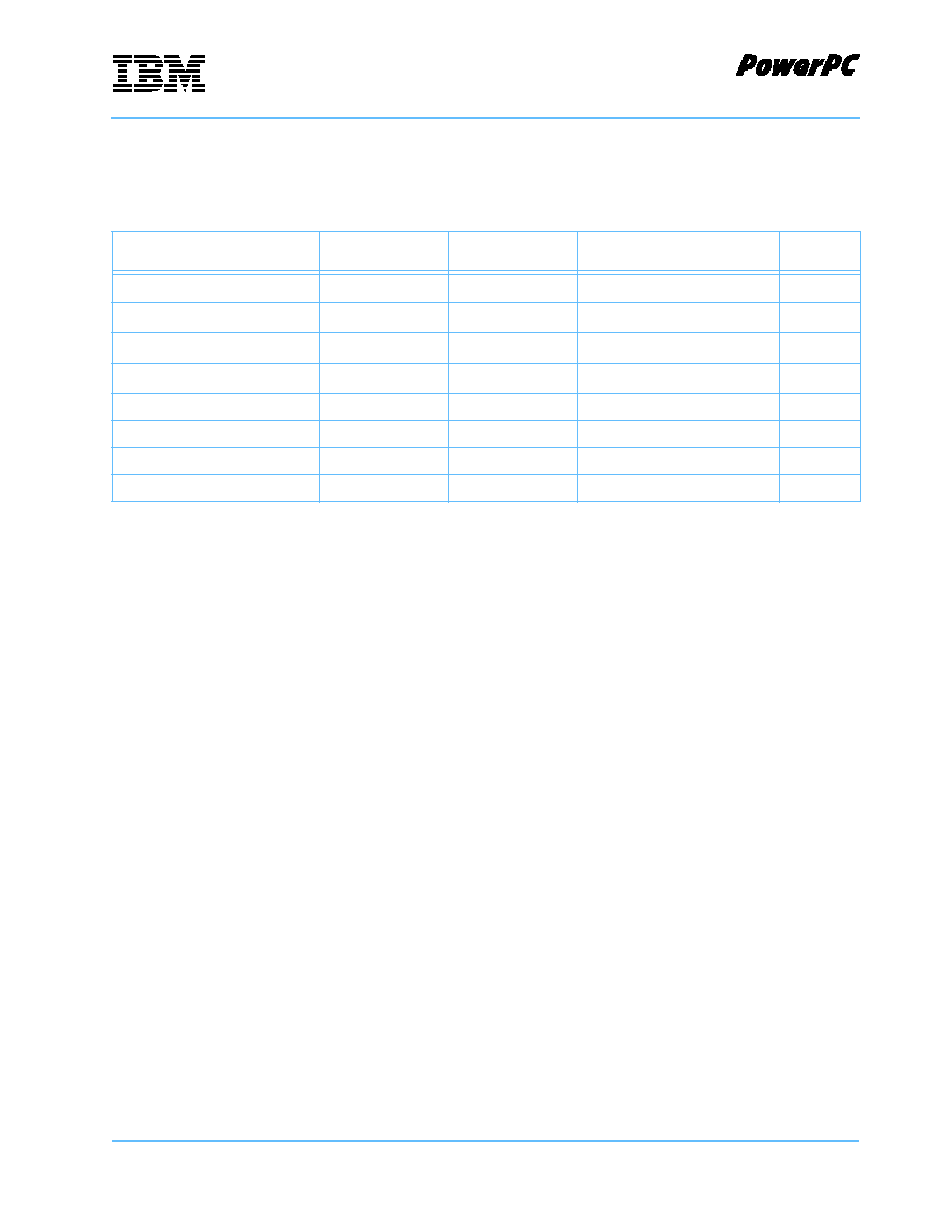
5. Ordering Information
For availability, contact your local IBM sales office.
Note 1: Previous versions of this document contained an error in the OEMLS part numbers of the parts shown.
The 45L7531, 09K4299, and 09K4298 part numbers showed a "B" in the Application Conditions field,
instead of "A", which is now shown correctly. All of these parts that were shipped by IBM were correctly
marked.
Note 2: Part number 45L7530 has a "B" in the OEMLS part number, and is marked with a "B" on the package and
in all revisions of the Datasheet. This part is actually specified for "A" application conditions. For this part
number, decode the "B" to mean "Full Specification." The OEMLS part number and package marking of
45L7530 will not be changed. This part number will not be issued with any other application conditions.
OEMLS Part Number
Internal IBM Part
Number
Processor Bus Fre-
quency
Shipping Package
Rev
Level
IBM25CPC700BB3A66
1
45L7531
66.66
Tray
dd 1.1
IBM25CPC700BB3B83
2
45L7530
83.33
Tray
dd 1.1
IBM25CPC700CB3A66
1
09K4299
66.66
Tray
dd 1.2
IBM25CPC700CB3A83
1
09K4298
83.33
Tray
dd 1.2
IBM25CPC700DB3A66
88H3097
66.66
Tray
dd 1.3
IBM25CPC700DB3A66Z
88H4076
66.66
Tape and Reel
dd 1.3
IBM25CPC700DB3A83
88H3096
83.33
Tray
dd 1.3
IBM25CPC700DB3A83Z
88H3990
83.33
Tape and Reel
dd 1.3
.

CPC700 Memory Controller and PCI Bridge
©IBM Corporation. All rights reserved.
Use is further subject to the provisions at the end of this document.
Page 20 of 22
CPC700
4/17/01
The following figure provides the part numbering nomenclature for the CPC700.
OEMLS Part Number Key
Marketing Part Number
IBM25CPC700DB3A83Z
Package
Processor Bus Frequency
Reliability
Application Conditions
B
A
Revision
PCI Rev Reg
dd 1.1
dd 1.0
0000 0000
0000 0001
66 = 66.66 MHz
83 = 83.33 MHz
A = Full Specification
dd 1.2
C
0000 0010
Code
Revision
Level
D
dd 1.3
0000 0011
Shipping Package
Blank = Tray
Z = Tape and reel
3= Grade 3
B = CBGA

CPC700 Memory Controller and PCI Bridge
CPC700
4/17/01
©IBM Corporation. All rights reserved.
Use is further subject to the provisions at the end of this document.
Page 21 of 22
Inside of back cover

CPC700 Memory Controller and PCI Bridge
©IBM Corporation. All rights reserved.
Use is further subject to the provisions at the end of this document.
Page 22 of 22
CPC700
4/17/01
Copyright
Trademarks
The following are trademarks of International Business Machines Corporation in the United States, or
other countries, or both:
IBM
IBM Logo
PowerPC
AIX
CPC700
Other company, product, and service names may be trademarks or service marks of others.
IBM reserves the right to change or discontinue this product without notice.
© International Business Machines Corporation 2001.
Portions hereof ©International Business Machines Corporation, 1991-2001.
All rights reserved.