 | –≠–Ľ–Ķ–ļ—ā—Ä–ĺ–Ĺ–Ĺ—č–Ļ –ļ–ĺ–ľ–Ņ–ĺ–Ĺ–Ķ–Ĺ—ā: IBMCPC710 | –°–ļ–į—á–į—ā—Ć:  PDF PDF  ZIP ZIP |

Preliminary
CPC710 PCI Bridge and Memory Controller Data Sheet
1
Features
∑ IBM CPC710 PowerPC
to PCI bridge
- 2.5V PPC60x processor bus running at up
to 133MHz
- Dual 32- and 64-bit PCI interfaces
- 100- and 133-MHz SDRAM interface
- Internal DMA controller
- 2-MB Flash boot ROM support
- 256-MB Extended Flash support
- JTAG for board level testing
∑ PCI interfaces
- Two independent bridges with parking
- PCI Revision 2.1 compliant
- 3.3V signal interface
∑ Synchronous DRAM (SDRAM) interface
operating at 100 or 133 MHz
- Support for PC100 and PC133 SDRAM and
Registered DIMMs
- Two-way interleaved operation with ECC
using external multiplexer
- Up to 3.5GB addressing space using 16-,
64-,128-, 256-, 512- or 1024-MB DIMMs
∑ PPC60x Bus interface
- Up to 133MHz bus
- One to four processors
- Up to 6 outstanding transaction requests
- Little Endian mode available
∑ System I/O interface
- 2-MB Flash Boot ROM
- 256-MB Extended Flash
∑ DMA controller
- Single channel
- System memory-to-PCI transfers only
- Store-gather for enhanced performance
Description
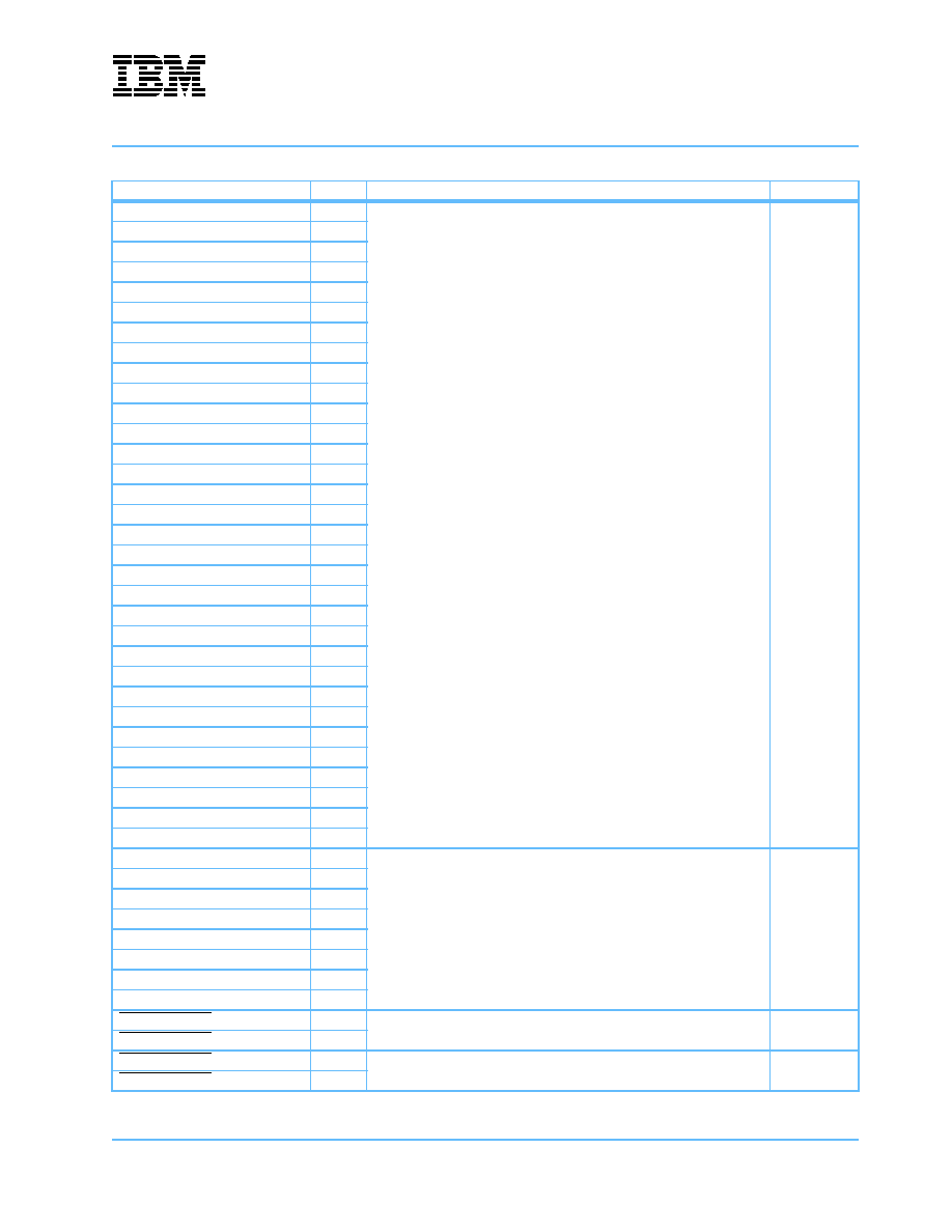
The CPC710 IBM PCI Bridge and Memory
Controller is a highly integrated host bridge device
that interfaces PowerPC 60x buses to SDRAM-
based system memory and also provides two PCI
interfaces. It supports up to four processors with
pipelining for up to six outstanding transaction
requests.
The memory controller supports SDRAM, allowing
the memory to burst data on most bus cycles at
100MHz or 133 MHz.
For system designs requiring high I/O bandwidth,
there are two PCI host bus bridges. One bridge
supports a standard 32-bit, 33MHz PCI bus, while
the other supports 64 bits at up to 66 MHz for
graphics and high speed communications.
An internal DMA controller allows high speed data
transfer between Memory and I/O. Store-gathering
enhances the CPU-to-I/O performance.
Technology: IBM CMOS SA-12E, 0.25
Ķ
m
Package: 35mm, 728-ball flip chip-plastic ball grid
array (FC-PBGA)
Power (estimated): Typical 2.1 W, Maximum 2.6W
While the information contained herein is believed to be accurate, such information is preliminary, and should not be
relied upon for accuracy or completeness, and no representations or warranties of accuracy or completeness are made.

Preliminary
CPC710 PCI Bridge and Memory Controller Data Sheet
2
Contents
Ordering Information . . . . . . . . . . . . . . . . . . . . . . . . . . . . . . . . . . . . . . . . . . . . . . . . . . . . . . . . . . . . . . . . . . . . 3
Features . . . . . . . . . . . . . . . . . . . . . . . . . . . . . . . . . . . . . . . . . . . . . . . . . . . . . . . . . . . . . . . . . . . . . . . . . . . . . 5
60x Bus Interface . . . . . . . . . . . . . . . . . . . . . . . . . . . . . . . . . . . . . . . . . . . . . . . . . . . . . . . . . . . . . . . . . . . . . . 5
SDRAM Memory Controller . . . . . . . . . . . . . . . . . . . . . . . . . . . . . . . . . . . . . . . . . . . . . . . . . . . . . . . . . . . . . . 5
PCI Bridges . . . . . . . . . . . . . . . . . . . . . . . . . . . . . . . . . . . . . . . . . . . . . . . . . . . . . . . . . . . . . . . . . . . . . . . . . . . 6
JTAG . . . . . . . . . . . . . . . . . . . . . . . . . . . . . . . . . . . . . . . . . . . . . . . . . . . . . . . . . . . . . . . . . . . . . . . . . . . . . . . . 6
Signal Lists . . . . . . . . . . . . . . . . . . . . . . . . . . . . . . . . . . . . . . . . . . . . . . . . . . . . . . . . . . . . . . . . . . . . . . . . . . . 8
Signal Descriptions . . . . . . . . . . . . . . . . . . . . . . . . . . . . . . . . . . . . . . . . . . . . . . . . . . . . . . . . . . . . . . . . . . . . 35
Figures
CPC710 PCI Bridge and Memory Controller Functional Block Diagram . . . . . . . . . . . . . . . . . . . . . . . . . . . . 4
35mm, 728-Ball FC-PBGA Package . . . . . . . . . . . . . . . . . . . . . . . . . . . . . . . . . . . . . . . . . . . . . . . . . . . . . . . 7
AC Input Timing Waveform . . . . . . . . . . . . . . . . . . . . . . . . . . . . . . . . . . . . . . . . . . . . . . . . . . . . . . . . . . . . . . 47
Tables
Signals Listed Alphabetically . . . . . . . . . . . . . . . . . . . . . . . . . . . . . . . . . . . . . . . . . . . . . . . . . . . . . . . . . . . . . 8
Signals Listed by Ball Assignment . . . . . . . . . . . . . . . . . . . . . . . . . . . . . . . . . . . . . . . . . . . . . . . . . . . . . . . . 28
Pin Summary . . . . . . . . . . . . . . . . . . . . . . . . . . . . . . . . . . . . . . . . . . . . . . . . . . . . . . . . . . . . . . . . . . . . . . . . 35
Signal Functional Description . . . . . . . . . . . . . . . . . . . . . . . . . . . . . . . . . . . . . . . . . . . . . . . . . . . . . . . . . . . . 36
Absolute Maximum Ratings . . . . . . . . . . . . . . . . . . . . . . . . . . . . . . . . . . . . . . . . . . . . . . . . . . . . . . . . . . . . . 45
Package Thermal Specifications . . . . . . . . . . . . . . . . . . . . . . . . . . . . . . . . . . . . . . . . . . . . . . . . . . . . . . . . . . 45
Recommended DC Operating Conditions . . . . . . . . . . . . . . . . . . . . . . . . . . . . . . . . . . . . . . . . . . . . . . . . . . . 46
AC Timing Specifications . . . . . . . . . . . . . . . . . . . . . . . . . . . . . . . . . . . . . . . . . . . . . . . . . . . . . . . . . . . . . . . 47
Clock Timing . . . . . . . . . . . . . . . . . . . . . . . . . . . . . . . . . . . . . . . . . . . . . . . . . . . . . . . . . . . . . . . . . . . . . . . . . 47
I/O Specifications--133 MHz . . . . . . . . . . . . . . . . . . . . . . . . . . . . . . . . . . . . . . . . . . . . . . . . . . . . . . . . . . . . 48
I/O Specifications--100 MHz . . . . . . . . . . . . . . . . . . . . . . . . . . . . . . . . . . . . . . . . . . . . . . . . . . . . . . . . . . . . 50
PCI I/O Specifications--133 MHz . . . . . . . . . . . . . . . . . . . . . . . . . . . . . . . . . . . . . . . . . . . . . . . . . . . . . . . . . 52
PCI I/O Specifications--100 MHz . . . . . . . . . . . . . . . . . . . . . . . . . . . . . . . . . . . . . . . . . . . . . . . . . . . . . . . . . 53
Preliminary
CPC710 PCI Bridge and Memory Controller Data Sheet
3
Ordering Information
This section provides the part numbering nomenclature for the CPC710. For availability, contact your local
IBM sales office.
Each part number contains a revision code. This refers to the die mask revision number and is specified in
the part numbering scheme for identification purposes only.
IBM Part Number Key
Product Name
Order Part Number
Processor Bus Frequency
Package
Revision
Level
CPC710-100
IBM25CPC710CF3A100
100MHz
35 mm, 728-ball FC-PBGA
C
CPC710-133
IBM25CPC710CF3B133
133MHz
35 mm, 728-ball FC-PBGA
C
IBM Part Number
IBM25CPC710CF3B133
60x/Memory Bus Speed
Grade 3 Reliability
Junction Temperature Range
B = - 40 įC to + 85įC
100 = 100MHz
Revision Code
Package (FC-PBGA)
133 = 133 MHz
A = - 40 įC to + 105įC

Preliminary
CPC710 PCI Bridge and Memory Controller Data Sheet
4
CPC710 PCI Bridge and Memory Controller Functional Block Diagram
SDRAM
Controller
Clock,
Reset,
JTAG
72 bits
133MHz max
Bridge
64 bits
66 MHz max
PCI-64
Bridge
PCI-32
32 bits
33 MHz
DMA
60x Interface Logic
60x/750 PowerPC
CPC710
64 bits data
32 bits addr
133MHz max
SIO
Interface
- Data
Controller
- Flash memory
- External Registers
- Address
Control

Preliminary
CPC710 PCI Bridge and Memory Controller Data Sheet
5
Features
∑ Up to 133MHz PowerPC 60x 64-bit bus
∑ 2.5V 60x PowerPC bus
∑ Supports 100- and 133-MHz SDRAM including PC100 and PC133
∑ Up to 2MB Flash Boot ROM support
∑ 32-bit 33MHz/64-bit 33-66MHz asynchronous dual PCI buses
∑ Bidirectional interface to two external 32-bit registers
∑ PreP and CHRP compliant design
∑ One-channel chained DMA controller
∑ Up to 256-MB Extended Flash support
∑ 32-bit PCI bus has 3.3V, 5V-tolerant I/O
∑ 64-bit PCI bus has 3.3V I/O
∑ Power dissipation estimate of 2.1W at 133MHz
∑ PLL to reduce on-chip system clock skew
∑ JTAG controller
60x Bus Interface
∑ Supports 740L/750L, 750CX/Cxe, or 74xx PowerPC
∑ Up 133-MHz external bus operation
∑ Supports four processors
∑ 64-bit data bus with 8 bits of parity
∑ 32-bit address bus with 4 bits of parity
∑ Dual 32-byte store back buffers
∑ High bandwidth, 4-way arbiter
∑ Little Endian mode PowerPC
∑ Supports SYNC/EIEIO ordering operations
∑ Supports L2 cache or bus slaves with external decode
SDRAM Memory Controller
The CPC710 Memory Controller core provides a low latency access path to SDRAM memory. A variety of
system memory configurations are supported.
Features include:
∑ Support for 100- and 133-MHz SDRAM including PC100 and PC133 and Registered DIMMs
∑ Supports 16-, 64-, 128-, and 256-Mbit SDRAMs
∑ Up to 3.5 GB addressing range using 16-, 64-,128-, 256-, 512- or 1024-MB DIMMs
∑ 2-way interleaved SDRAM with ECC (external MUX to reduce pin count)
∑ Programmable timing parameters
∑ Up to 6 dual bank DIMMs
∑ Up to 4 banks supported for Multibanking
∑ SDRAM Access command queue with look ahead override option for CPU, PCIs, and DMA
∑ Access based on 32-byte cache line reload
∑ Three separate dual 32-byte load buffers (PCI-32, PCI-64, 60x)

Preliminary
CPC710 PCI Bridge and Memory Controller Data Sheet
6
PCI Bridges
∑ Two independent PCI bus bridges with parking
∑ PCI revision 2.1 compliant
∑ PCI-32 with 3.3V, 5V tolerant interface
∑ PCI-64 with 3.3 V interface
∑ Buses run asynchronously to processor and memory controller
∑ External arbitration available for both buses
∑ Dual 32-byte buffers in each PCI bridge
∑ Round-robin PCI arbiter
∑ Coherency for memory access through DMA controller or through PCI master
JTAG
∑ IEEE 1149.1 Test Access Port (TAP)
∑ IBM RISCWatch Debugger support

Preliminary
CPC710 PCI Bridge and Memory Controller Data Sheet
7
35mm, 728-Ball FC-PBGA Package
A
1.27
26
AF
35.0Ī0.2
35.0 Ī0.2
0.5 to 0.7
B
C
D
E
F
G
H
J
K
L
M
AA
N
P
R
T
U
V
W
Y
AB
AC
AD
AE
01 03 05 07 09 11 13 15 17 19
02 04 06 08 10 12 14 16 18
21 23 25
20 22 24
Top View
Bottom View
Note: All dimensions are in mm.
AG
27
0.6 to 0.9 dia.
solder ball
3.45 max
Lid
Chip
Index corner (missing A01 ball)
Index mark
A01 corner
Preliminary
CPC710 PCI Bridge and Memory Controller Data Sheet
8
Signal Lists
The following table lists all the external signals in alphabetical order and shows the ball number on which the
signal appears. Multiplexed signals are shown with the default signal (following reset)
not
in brackets and the
alternate signal in brackets. Multiplexed signals appear alphabetically multiple times in the list--once for each
signal name on the ball. The page number listed gives the page in "Signal Functional Description" on page 36
where the signals in the indicated interface group begin.
Signals Listed Alphabetically
(Part 1 of 20)
Signal Name
Ball
Interface Group
Page
AV
DD
D27
Power
44
BS0
J10
SDRAM
39
BS1
J09
CE0_TEST
N23
System
43
CHKSTOP
J26
60x
36
DLK
G06
60x
36
FLASH_CE
G27
SIO
42
FLASH_OE
H27
FLASH_WE
H26

Preliminary
CPC710 PCI Bridge and Memory Controller Data Sheet
9
GND
A03
Power
44
GND
A11
GND
A17
GND
A25
GND
C01
GND
C05
GND
C09
GND
C13
GND
C15
GND
C19
GND
C23
GND
C27
GND
E03
GND
E07
GND
E11
GND
E17
GND
E21
GND
E25
GND
F14
GND
G05
GND
G09
GND
G19
GND
G23
GND
H12
GND
H16
GND
J03
GND
J07
GND
J21
GND
J25
GND
L01
GND
L05
Signals Listed Alphabetically
(Part 2 of 20)
Signal Name
Ball
Interface Group
Page

Preliminary
CPC710 PCI Bridge and Memory Controller Data Sheet
10
GND
L23
Power
44
GND
L27
GND
M08
GND
M20
GND
N03
GND
N13
GND
N15
GND
N25
GND
P06
GND
P14
GND
P22
GND
R03
GND
R13
GND
R15
GND
R25
GND
T08
GND
T20
GND
U01
GND
U05
GND
U23
GND
U27
GND
W03
GND
W07
GND
W21
GND
W25
GND
Y12
GND
Y16
GND
AA05
GND
AA09
GND
AA19
GND
AA23
GND
AB14
GND
AC03
GND
AC07
GND
AC11
GND
AC17
GND
AC21
GND
AC25
GND
AE01
GND
AE05
GND
AE09
GND
AE13
GND
AE15
Signals Listed Alphabetically
(Part 3 of 20)
Signal Name
Ball
Interface Group
Page

Preliminary
CPC710 PCI Bridge and Memory Controller Data Sheet
11
GND
AE19
Power
44
GND
AE23
GND
AE27
GND
AG03
GND
AG11
GND
AG17
GND
AG25
GPIO0
H25
60x
36
GPIO1
F25
GPIO2
D25
G_ACK64
R06
PCI-64
41
G_ADH00
AD02
PCI-64
41
G_ADH01
AE02
G_ADH02
AC02
G_ADH03
AB01
G_ADH04
AA02
G_ADH05
AA01
G_ADH06
Y02
G_ADH07
Y01
G_ADH08
W02
G_ADH09
V03
G_ADH10
V02
G_ADH11
V01
G_ADH12
U02
G_ADH13
T04
G_ADH14
T03
G_ADH15
T02
G_ADH16
T01
G_ADH17
R04
G_ADH18
R02
G_ADH19
R01
G_ADH20
P03
G_ADH21
P02
G_ADH22
N07
G_ADH23
N06
G_ADH24
N05
G_ADH25
N04
G_ADH26
N02
G_ADH27
N01
G_ADH28
M04
G_ADH29
M03
G_ADH30
M02
G_ADH31
M01
Signals Listed Alphabetically
(Part 4 of 20)
Signal Name
Ball
Interface Group
Page

Preliminary
CPC710 PCI Bridge and Memory Controller Data Sheet
12
G_ADL00
M09
PCI-64
41
G_ADL01
M07
G_ADL02
M06
G_ADL03
M05
G_ADL04
L09
G_ADL05
L08
G_ADL06
L06
G_ADL07
L04
G_ADL08
L02
G_ADL09
K07
G_ADL10
K06
G_ADL11
K05
G_ADL12
K04
G_ADL13
K03
G_ADL14
K02
G_ADL15
K01
G_ADL16
J06
G_ADL17
J04
G_ADL18
J02
G_ADL19
H05
G_ADL20
H04
G_ADL21
H03
G_ADL22
H02
G_ADL23
H01
G_ADL24
G04
G_ADL25
G02
G_ADL26
G01
G_ADL27
F03
G_ADL28
F02
G_ADL29
F01
G_ADL30
E02
G_ADL31
D01
G_ARB[SDDQM]
H06
PCI-64
41
G_CBE0
V09
PCI-64
41
G_CBE1
U09
G_CBE2
U08
G_CBE3
R07
G_CBE4
R05
G_CBE5
P09
G_CBE6
P07
G_CBE7
P05
G_DEVSEL
AB04
PCI-64
41
G_FRAME
B01
PCI-64
41
Signals Listed Alphabetically
(Part 5 of 20)
Signal Name
Ball
Interface Group
Page

Preliminary
CPC710 PCI Bridge and Memory Controller Data Sheet
13
G_GNT0
AA04
PCI-64
41
G_GNT1
Y05
G_GNT2
Y04
G_GNT3
Y03
G_GNT4
W04
G_GNT5[P_GNT4]
V05
G_GNT6[P_GNT5]
V04
G_GNT7[P_GNT6]
U04
G_IDSEL
AD03
PCI-64
41
G_INTA
T09
PCI-64
41
G_INTB
T07
G_INTC
T06
G_INTD
T05
G_IRDY
K09
PCI-64
41
G_LOCK
AC04
PCI-64
41
G_PAR
R08
PCI-64
41
G_PAR64
AB05
PCI-64
41
G_PERR
F04
PCI-64
41
G_REQ0
U06
PCI-64
41
G_REQ1
V06
G_REQ2
V07
G_REQ3
W06
G_REQ4
Y06
G_REQ5[P_REQ4]
Y07
G_REQ6[P_REQ5]
Y09
G_REQ7[P_REQ6]
AA06
G_REQ64
AB03
PCI-64
41
G_RESETOUT
AD01
PCI-64
41
G_RST
D02
PCI-64
41
G_SERR
AB02
PCI-64
41
G_STOP
N08
PCI-64
41
G_TRDY
J08
PCI-64
41
IT1
E22
60x
36
IT2
E24
MADDR0_EVEN
C18
SDRAM
39
MADDR0_ODD
D17
Signals Listed Alphabetically
(Part 6 of 20)
Signal Name
Ball
Interface Group
Page

Preliminary
CPC710 PCI Bridge and Memory Controller Data Sheet
14
MADDR01
D18
SDRAM
39
MADDR02
E18
MADDR03
E20
MADDR04
F17
MADDR05
F18
MADDR06
F19
MADDR07
F20
MADDR08
F21
MADDR09
F22
MADDR10
G18
MADDR11
G20
MADDR12
H17
MADDR13
H19
MDATA00
A04
SDRAM
39
MDATA01
A06
MDATA02
A07
MDATA03
A08
MDATA04
A10
MDATA05
A12
MDATA06
A13
MDATA07
A15
MDATA08
A16
MDATA09
B04
MDATA10
B05
MDATA11
B06
MDATA12
B07
MDATA13
B08
MDATA14
B09
MDATA15
B10
MDATA16
B11
MDATA17
B12
MDATA18
B13
MDATA19
B14
MDATA20
B15
MDATA21
B16
MDATA22
B17
MDATA23
C04
MDATA24
C06
MDATA25
C08
MDATA26
C10
MDATA27
C12
MDATA28
C14
MDATA29
C16
MDATA30
D05
MDATA31
D06
Signals Listed Alphabetically
(Part 7 of 20)
Signal Name
Ball
Interface Group
Page
Preliminary
CPC710 PCI Bridge and Memory Controller Data Sheet
15
MDATA32
D07
SDRAM
39
MDATA33
D08
MDATA34
D09
MDATA35
D10
MDATA36
D11
MDATA37
D12
MDATA38
D13
MDATA39
D15
MDATA40
D16
MDATA41
E06
MDATA42
E08
MDATA43
E10
MDATA44
E12
MDATA45
E13
MDATA46
E14
MDATA47
E15
MDATA48
E16
MDATA49
F07
MDATA50
F08
MDATA51
F09
MDATA52
F10
MDATA53
F11
MDATA54
F12
MDATA55
F13
MDATA56
F15
MDATA57
F16
MDATA58
G08
MDATA59
G10
MDATA60
G12
MDATA61
G13
MDATA62
G14
MDATA63
G15
MDATA64
G16
SDRAM
39
MDATA65
H11
MDATA66
H13
MDATA67
H15
MDATA68
J11
MDATA69
J12
MDATA70
J14
MDATA71
J16
MUX_CLKENA1
F06
SDRAM
39
MUX_CLKENA2
H07
MUX_CLKEN1B
J17
SDRAM
39
MUX_CLKEN2B
J18
Signals Listed Alphabetically
(Part 8 of 20)
Signal Name
Ball
Interface Group
Page

Preliminary
CPC710 PCI Bridge and Memory Controller Data Sheet
16
MUX_OEA
B03
SDRAM
39
MUX_OEB
C02
MUX_SEL
D04
SDRAM
39
NODLK
A02
60x
36
No pin
A01
OV
DD
E27
Power
OV
DD
G25
OV
DD
J23
OV
DD
L21
OV
DD
P20
OV
DD
P27
OV
DD
U21
OV
DD
W23
OV
DD
AA25
OV
DD
AC27
OV
DD
Y14
OV
DD
AA11
OV
DD
AA17
OV
DD
AC09
OV
DD
AC19
OV
DD
AE07
OV
DD
AE21
OV
DD
AG05
OV
DD
AG14
OV
DD
AG23
OV
DD
E01
OV
DD
G03
OV
DD
J05
OV
DD
L07
Signals Listed Alphabetically
(Part 9 of 20)
Signal Name
Ball
Interface Group
Page
Preliminary
CPC710 PCI Bridge and Memory Controller Data Sheet
17
OV
DD
P01
SDRAM
39
OV
DD
P08
OV
DD
U07
OV
DD
W05
OV
DD
AA03
OV
DD
AC01
OV
DD
A05
OV
DD
A14
OV
DD
A23
OV
DD
C07
OV
DD
C21
OV
DD
E09
OV
DD
E19
OV
DD
G11
OV
DD
G17
OV
DD
H14
PCG_CLK
W08
PCI-64
41
PCI_CLK
AB27
PCI-32
40
PLL_LOCK
P23
System
43
PLL_RANGE0
K27
System
43
PLL_RANGE1
F23
PLL_RESET
A27
System
43
PLL_TUNE0
B25
System
43
PLL_TUNE1
H20
PLL_TUNE2
T23
PLL_TUNE3
R27
PLL_TUNE4
R23
PLL_TUNE5
J20
POWERGOOD
AG06
System
43
PRES_OE0
B26
SIO
42
PRES_OE1
C26
Signals Listed Alphabetically
(Part 10 of 20)
Signal Name
Ball
Interface Group
Page
Preliminary
CPC710 PCI Bridge and Memory Controller Data Sheet
18
P_ADL00
P26
PCI-32
40
P_ADL01
N26
P_ADL02
M26
P_ADL03
L26
P_ADL04
K26
P_ADL05
K25
P_ADL06
M25
P_ADL07
P25
P_ADL08
N24
P_ADL09
M24
P_ADL10
L24
P_ADL11
K24
P_ADL12
J24
P_ADL13
K23
P_ADL14
M23
P_ADL15
N22
P_ADL16
M22
P_ADL17
L22
P_ADL18
K22
P_ADL19
J22
P_ADL20
H22
P_ADL21
G22
P_ADL22
K21
P_ADL23
M21
P_ADL24
N21
P_ADL25
P21
P_ADL26
N20
P_ADL27
L20
P_ADL28
K19
P_ADL29
L19
P_ADL30
M19
P_ADL31
P19
P_CBE0
R24
PCI-32
40
P_CBE1
T24
P_CBE2
T25
P_CBE3
T26
P_DEVSEL
R22
PCI-32
40
P_FRAME
T22
PCI-32
40
P_GNT0
AA27
PCI-32
40
P_GNT1
Y27
P_GNT2
W26
P_GNT3
T27
[P_GNT4]G_GNT5
V05
[P_GNT5]G_GNT6
V04
[P_GNT6]G_GNT7
U04
Signals Listed Alphabetically
(Part 11 of 20)
Signal Name
Ball
Interface Group
Page

Preliminary
CPC710 PCI Bridge and Memory Controller Data Sheet
19
P_LOCK
H21
PCI-32
40
P_MEMACK
G24
PCI-32
40
P_MEMREQ
H24
PCI-32
40
P_PAR
H23
PCI-32
40
P_PERR
U26
PCI-32
40
P_REQ0
V27
PCI-32
40
P_REQ1
V26
P_REQ2
V25
P_REQ3
V24
[P_REQ4]G_REQ5
Y07
[P_REQ5]G_REQ6
Y09
[P_REQ6]G_REQ7
AA06
P_RST
N27
PCI-32
40
P_SERR
V23
PCI-32
40
P_STOP
U24
PCI-32
40
P_TRDY
M27
PCI-32
40
Reserved
J13
Other pins
Reserved
J15
Reserved
J19
Reserved
K10
Reserved
K11
Reserved
K12
Reserved
K13
Reserved
K14
Reserved
K15
Reserved
K16
Reserved
K17
Reserved
K18
Reserved
L10
Reserved
L11
Reserved
L12
Reserved
L13
Reserved
L14
Reserved
L15
Reserved
L16
Reserved
L17
Signals Listed Alphabetically
(Part 12 of 20)
Signal Name
Ball
Interface Group
Page
Preliminary
CPC710 PCI Bridge and Memory Controller Data Sheet
20
Reserved
L18
Other pins
Reserved
M10
Reserved
M11
Reserved
M12
Reserved
M13
Reserved
M14
Reserved
M15
Reserved
M16
Reserved
M17
Reserved
M18
Reserved
N09
Reserved
N10
Reserved
N11
Reserved
N12
Reserved
N16
Reserved
N17
Reserved
N18
Reserved
N19
Reserved
P10
Reserved
P11
Reserved
P12
Reserved
P16
Reserved
P17
Reserved
P18
Reserved
R09
Reserved
R10
Reserved
R11
Reserved
R12
Reserved
R16
Reserved
R17
Reserved
R18
Reserved
R19
Reserved
T10
Reserved
T11
Reserved
T12
Reserved
T13
Reserved
T14
Reserved
T15
Reserved
T16
Reserved
T17
Reserved
T18
Reserved
U10
Reserved
U11
Reserved
U12
Reserved
U13
Signals Listed Alphabetically
(Part 13 of 20)
Signal Name
Ball
Interface Group
Page
Preliminary
CPC710 PCI Bridge and Memory Controller Data Sheet
21
Reserved
U14
Other pins
Reserved
U15
Reserved
U16
Reserved
U17
Reserved
U18
Reserved
V10
Reserved
V11
Reserved
V12
Reserved
V13
Reserved
V14
Reserved
V15
Reserved
V16
Reserved
V17
Reserved
V18
Reserved
W09
Reserved
W13
Reserved
W15
Reserved
W19
SDCAS0
E04
SDRAM
39
SDCAS1[SDDQM]
F05
SDCKE0
A22
SDRAM
39
SDCKE1
A24
SDCKE2
A26
SDCKE3
B22
SDCKE4
B23
SDCKE5
B24
SDCKE6
C22
SDCKE7
C24
SDCKE8
D22
SDCKE9
D24
SDCS00
D23
SDRAM
39
SDCS01
D21
SDCS02
D20
SDCS03
D19
SDCS04
C20
SDCS05
B21
SDCS06
B20
SDCS07
B19
SDCS08
B18
SDCS09
A21
SDCS10
A20
SDCS11
A18
[SDDQM]G_ARB
[SDDQM]SDCAS1
[SDDQM]SDRAS1
[SDDQM]WE1
G06
F05
D03
H09
SDRAM
39
Signals Listed Alphabetically
(Part 14 of 20)
Signal Name
Ball
Interface Group
Page

Preliminary
CPC710 PCI Bridge and Memory Controller Data Sheet
22
SDRAS0
B02
SDRAM
39
SDRAS1[SDDQM]
D03
SYS_AACK
W10
60x
36
SYS_ADDR00
W24
60x
36
SYS_ADDR01
Y22
SYS_ADDR02
Y23
SYS_ADDR03
Y24
SYS_ADDR04
AA22
SYS_ADDR05
AA24
SYS_ADDR06
AB22
SYS_ADDR07
AB23
SYS_ADDR08
AB24
SYS_ADDR09
AB25
SYS_ADDR10
AB26
SYS_ADDR11
AC22
SYS_ADDR12
AC24
SYS_ADDR13
AC26
SYS_ADDR14
AD22
SYS_ADDR15
AD23
SYS_ADDR16
AD24
SYS_ADDR17
AD25
SYS_ADDR18
AD26
SYS_ADDR19
AD27
SYS_ADDR20
AE22
SYS_ADDR21
AE24
SYS_ADDR22
AE26
SYS_ADDR23
AF21
SYS_ADDR24
AF22
SYS_ADDR25
AF23
SYS_ADDR26
AF24
SYS_ADDR27
AF25
SYS_ADDR28
AF26
SYS_ADDR29
AF27
SYS_ADDR30
AG20
SYS_ADDR31
AG21
SYS_ADDRP0
Y21
60x
36
SYS_ADDRP1
W22
SYS_ADDRP2
V22
SYS_ADDRP3
V21
SYS_ARTRY
W11
60x
36
SYS_BG0
AF01
60x
36
SYS_BG1
Y20
SYS_BG2
Y25
SYS_BG3
AA26
Signals Listed Alphabetically
(Part 15 of 20)
Signal Name
Ball
Interface Group
Page

Preliminary
CPC710 PCI Bridge and Memory Controller Data Sheet
23
SYS_BR0
V19
60x
36
SYS_BR1
U19
SYS_BR2
T19
SYS_BR3
U20
SYS_CLK
B27
System
43
SYS_DATA00
Y08
System
43
SYS_DATA01
AA08
SYS_DATA02
AA10
SYS_DATA03
AA12
SYS_DATA04
AA13
SYS_DATA05
AA14
SYS_DATA06
AA15
SYS_DATA07
AA16
SYS_DATA08
AB08
SYS_DATA09
AB09
SYS_DATA10
AB10
SYS_DATA11
AB11
SYS_DATA12
AB12
SYS_DATA13
AB13
SYS_DATA14
AB15
SYS_DATA15
AB16
SYS_DATA16
AB17
SYS_DATA17
AB18
SYS_DATA18
AB19
SYS_DATA19
AC08
SYS_DATA20
AC10
SYS_DATA21
AC12
SYS_DATA22
AC13
SYS_DATA23
AC14
SYS_DATA24
AC15
SYS_DATA25
AC16
SYS_DATA26
AC18
SYS_DATA27
AD07
SYS_DATA28
AD08
SYS_DATA29
AD09
SYS_DATA30
AD10
SYS_DATA31
AD11
Signals Listed Alphabetically
(Part 16 of 20)
Signal Name
Ball
Interface Group
Page

Preliminary
CPC710 PCI Bridge and Memory Controller Data Sheet
24
SYS_DATA32
AD12
System
43
SYS_DATA33
AD13
SYS_DATA34
AD15
SYS_DATA35
AD16
SYS_DATA36
AD17
SYS_DATA37
AD18
SYS_DATA38
AE08
SYS_DATA39
AE10
SYS_DATA40
AE12
SYS_DATA41
AE14
SYS_DATA42
AE16
SYS_DATA43
AE18
SYS_DATA44
AF07
SYS_DATA45
AF08
SYS_DATA46
AF09
SYS_DATA47
AF10
SYS_DATA48
AF11
SYS_DATA49
AF12
SYS_DATA50
AF13
SYS_DATA51
AF14
SYS_DATA52
AF15
SYS_DATA53
AF16
SYS_DATA54
AF17
SYS_DATA55
AF18
SYS_DATA56
AG07
SYS_DATA57
AG08
SYS_DATA58
AG10
SYS_DATA59
AG12
SYS_DATA60
AG13
SYS_DATA61
AG15
SYS_DATA62
AG16
SYS_DATA63
AG18
SYS_DATAP0
AG04
System
43
SYS_DATAP1
AF03
SYS_DATAP2
AF04
SYS_DATAP3
AF06
SYS_DATAP4
AE04
SYS_DATAP5
AD05
SYS_DATAP6
AD06
SYS_DATAP7
AB07
SYS_DBG0
T21
System
43
SYS_DBG1
W20
SYS_DBG2
R21
SYS_DBG3
R20
SYS_GBL
Y11
System
43
Signals Listed Alphabetically
(Part 17 of 20)
Signal Name
Ball
Interface Group
Page

Preliminary
CPC710 PCI Bridge and Memory Controller Data Sheet
25
SYS_HRESET0
AD20
System
43
SYS_HRESET1
AC20
SYS_HRESET2
AE20
SYS_HRESET3
AD19
SYS_L2_HIT
AF02
System
43
SYS_MCP0
W14
System
43
SYS_MCP1
Y15
SYS_MCP2
W12
SYS_MCP3
Y13
SYS_SHD
AF05
System
43
SYS_SRESET0
AD21
System
43
SYS_SRESET1
AB21
SYS_SRESET2
AB20
SYS_SRESET3
AA20
SYS_TA
AG01
System
43
SYS_TA_HIT
AC06
System
43
SYS_TBE
AD04
System
43
SYS_TBST
AE06
System
43
SYS_TEA
AB06
System
43
SYS_TS
Y26
System
43
SYS_TSIZ0
AF19
System
43
SYS_TSIZ1
AF20
SYS_TSIZ2
AG02
SYS_TT0
AA18
System
43
SYS_TT1
W18
SYS_TT2
W17
SYS_TT3
Y17
SYS_TT4
W16
TCK
Y19
JTAG
48
TDI
E26
TDO
F27
TMS
R26
TRST
D26
V
DD
A09
Power
V
DD
A19
V
DD
C03
V
DD
C11
V
DD
C17
Signals Listed Alphabetically
(Part 18 of 20)
Signal Name
Ball
Interface Group
Page

Preliminary
CPC710 PCI Bridge and Memory Controller Data Sheet
26
V
DD
C25
Power
V
DD
D14
V
DD
E05
V
DD
E23
V
DD
G07
V
DD
G21
V
DD
H10
V
DD
H18
V
DD
J01
V
DD
J27
V
DD
K08
V
DD
K20
V
DD
L03
V
DD
L25
V
DD
N14
V
DD
P04
V
DD
P13
V
DD
P15
V
DD
P24
V
DD
R14
V
DD
U03
V
DD
U25
V
DD
V08
V
DD
V20
V
DD
W01
V
DD
W27
V
DD
Y10
V
DD
Y18
V
DD
AA07
V
DD
AA21
V
DD
AC05
V
DD
AC23
V
DD
AD14
V
DD
AE03
V
DD
AE11
V
DD
AE17
V
DD
AE25
V
DD
AG09
V
DD
AG19
Signals Listed Alphabetically
(Part 19 of 20)
Signal Name
Ball
Interface Group
Page
Preliminary
CPC710 PCI Bridge and Memory Controller Data Sheet
27
WE0
H08
SDRAM
39
WE1[SDDQM]
H09
XADR_LAT
G26
SIO
42
XCVR_RD
F26
Signals Listed Alphabetically
(Part 20 of 20)
Signal Name
Ball
Interface Group
Page

Preliminary
CPC710 PCI Bridge and Memory Controller Data Sheet
28
Signals Listed by Ball Assignment
(Part 1 of 7)
Ball
Signal Name
Ball
Signal Name
Ball
Signal Name
Ball
Signal Name
A01
No pin
B01
G_FRAME
C01
GND
D01
G_ADL31
A02
NODLK
B02
SDRAS0
C02
MUX_OEB
D02
G_RST
A03
GND
B03
MUX_OEA
C03
V
DD
D03
SDRAS1
A04
MDATA00
B04
MDATA09
C04
MDATA23
D04
MUX_SEL
A05
OV
DD
B05
MDATA10
C05
GND
D05
MDATA30
A06
MDATA01
B06
MDATA11
C06
MDATA24
D06
MDATA31
A07
MDATA02
B07
MDATA12
C07
OV
DD
D07
MDATA32
A08
MDATA03
B08
MDATA13
C08
MDATA25
D08
MDATA33
A09
V
DD
B09
MDATA14
C09
GND
D09
MDATA34
A10
MDATA04
B10
MDATA15
C10
MDATA26
D10
MDATA35
A11
GND
B11
MDATA16
C11
V
DD
D11
MDATA36
A12
MDATA05
B12
MDATA17
C12
MDATA27
D12
MDATA37
A13
MDATA06
B13
MDATA18
C13
GND
D13
MDATA38
A14
OV
DD
B14
MDATA19
C14
MDATA28
D14
V
DD
A15
MDATA07
B15
MDATA20
C15
GND
D15
MDATA39
A16
MDATA08
B16
MDATA21
C16
MDATA29
D16
MDATA40
A17
GND
B17
MDATA22
C17
V
DD
D17
MADDR0_ODD
A18
SDCS11
B18
SDCS08
C18
MADDR0_EVEN
D18
MADDR01
A19
V
DD
B19
SDCS07
C19
GND
D19
SDCS03
A20
SDCS10
B20
SDCS06
C20
SDCS04
D20
SDCS02
A21
SDCS09
B21
SDCS05
C21
OV
DD
D21
SDCS01
A22
SDCKE0
B22
SDCKE3
C22
SDCKE6
D22
SDCKE8
A23
OV
DD
B23
SDCKE4
C23
GND
D23
SDCS00
A24
SDCKE1
B24
SDCKE5
C24
SDCKE7
D24
SDCKE9
A25
GND
B25
PLL_TUNE0
C25
V
DD
D25
GPIO2
A26
SDCKE2
B26
PRES_OE0
C26
PRES_OE1
D26
TRST
A27
PLL_RESET
B27
SYS_CLK
C27
GND
D27
AV
DD
Preliminary
CPC710 PCI Bridge and Memory Controller Data Sheet
29
E01
OV
DD
F01
G_ADL29
G01
G_ADL26
H01
G_ADL23
E02
G_ADL30
F02
G_ADL28
G02
G_ADL25
H02
G_ADL22
E03
GND
F03
G_ADL27
G03
OV
DD
H03
G_ADL21
E04
SDCAS0
F04
G_PERR
G04
G_ADL24
H04
G_ADL20
E05
V
DD
F05
SDCAS1
G05
GND
H05
G_ADL19
E06
MDATA41
F06
MUX_CLKENA1
G06
DLK
H06
G_ARB
E07
GND
F07
MDATA49
G07
V
DD
H07
MUX_CLKENA2
E08
MDATA42
F08
MDATA50
G08
MDATA58
H08
WE0
E09
OV
DD
F09
MDATA51
G09
GND
H09
WE1
E10
MDATA43
F10
MDATA52
G10
MDATA59
H10
V
DD
E11
GND
F11
MDATA53
G11
OV
DD
H11
MDATA65
E12
MDATA44
F12
MDATA54
G12
MDATA60
H12
GND
E13
MDATA45
F13
MDATA55
G13
MDATA61
H13
MDATA66
E14
MDATA46
F14
GND
G14
MDATA62
H14
OV
DD
E15
MDATA47
F15
MDATA56
G15
MDATA63
H15
MDATA67
E16
MDATA48
F16
MDATA57
G16
MDATA64
H16
GND
E17
GND
F17
MADDR04
G17
OV
DD
H17
MADDR12
E18
MADDR02
F18
MADDR05
G18
MADDR10
H18
V
DD
E19
OV
DD
F19
MADDR06
G19
GND
H19
MADDR13
E20
MADDR03
F20
MADDR07
G20
MADDR11
H20
PLL_TUNE1
E21
GND
F21
MADDR08
G21
V
DD
H21
P_LOCK
E22
IT1
F22
MADDR09
G22
P_ADL21
H22
P_ADL20
E23
V
DD
F23
PLL_RANGE1
G23
GND
H23
P_PAR
E24
IT2
F24
P_IRDY
G24
P_MEMACK
H24
P_MEMREQ
E25
GND
F25
GPIO1
G25
OV
DD
H25
GPIO0
E26
TDI
F26
XCVR_RD
G26
XADR_LAT
H26
FLASH_WE
E27
OV
DD
F27
TDO
G27
FLASH_CE
H27
FLASH_OE
Signals Listed by Ball Assignment
(Part 2 of 7)
Ball
Signal Name
Ball
Signal Name
Ball
Signal Name
Ball
Signal Name

Preliminary
CPC710 PCI Bridge and Memory Controller Data Sheet
30
J01
V
DD
K01
G_ADL15
L01
GND
M01
G_ADH31
J02
G_ADL18
K02
G_ADL14
L02
G_ADL08
M02
G_ADH30
J03
GND
K03
G_ADL13
L03
V
DD
M03
G_ADH29
J04
G_ADL17
K04
G_ADL12
L04
G_ADL07
M04
G_ADH28
J05
OV
DD
K05
G_ADL11
L05
GND
M05
G_ADL03
J06
G_ADL16
K06
G_ADL10
L06
G_ADL06
M06
G_ADL02
J07
GND
K07
G_ADL09
L07
OV
DD
M07
G_ADL01
J08
G_TRDY
K08
V
DD
L08
G_ADL05
M08
GND
J09
BS1
K09
G_IRDY
L09
G_ADL04
M09
G_ADL00
J10
BS0
K10
Reserved
L10
Reserved
M10
Reserved
J11
MDATA68
K11
Reserved
L11
Reserved
M11
Reserved
J12
MDATA69
K12
Reserved
L12
Reserved
M12
Reserved
J13
Reserved
K13
Reserved
L13
Reserved
M13
Reserved
J14
MDATA70
K14
Reserved
L14
Reserved
M14
Reserved
J15
Reserved
K15
Reserved
L15
Reserved
M15
Reserved
J16
MDATA71
K16
Reserved
L16
Reserved
M16
Reserved
J17
MUX_CLKEN1B
K17
Reserved
L17
Reserved
M17
Reserved
J18
MUX_CLKEN2B
K18
Reserved
L18
Reserved
M18
Reserved
J19
Reserved
K19
P_ADL28
L19
P_ADL29
M19
P_ADL30
J20
PLL_TUNE5
K20
V
DD
L20
P_ADL27
M20
GND
J21
GND
K21
P_ADL22
L21
OV
DD
M21
P_ADL23
J22
P_ADL19
K22
P_ADL18
L22
P_ADL17
M22
P_ADL16
J23
OV
DD
K23
P_ADL13
L23
GND
M23
P_ADL14
J24
P_ADL12
K24
P_ADL11
L24
P_ADL10
M24
P_ADL09
J25
GND
K25
P_ADL05
L25
V
DD
M25
P_ADL06
J26
CHKSTOP
K26
P_ADL04
L26
P_ADL03
M26
P_ADL02
J27
V
DD
K27
PLL_RANGE0
L27
GND
M27
P_TRDY
Signals Listed by Ball Assignment
(Part 3 of 7)
Ball
Signal Name
Ball
Signal Name
Ball
Signal Name
Ball
Signal Name

Preliminary
CPC710 PCI Bridge and Memory Controller Data Sheet
31
N01
G_ADH27
P01
OV
DD
R01
G_ADH19
T01
G_ADH16
N02
G_ADH26
P02
G_ADH21
R02
G_ADH18
T02
G_ADH15
N03
GND
P03
G_ADH20
R03
GND
T03
G_ADH14
N04
G_ADH25
P04
V
DD
R04
G_ADH17
T04
G_ADH13
N05
G_ADH24
P05
G_CBE7
R05
G_CBE4
T05
G_INTD
N06
G_ADH23
P06
GND
R06
G_ACK64
T06
G_INTC
N07
G_ADH22
P07
G_CBE6
R07
G_CBE3
T07
G_INTB
N08
G_STOP
P08
OV
DD
R08
G_PAR
T08
GND
N09
Reserved
P09
G_CBE5
R09
Reserved
T09
G_INTA
N10
Reserved
P10
Reserved
R10
Reserved
T10
Reserved
N11
Reserved
P11
Reserved
R11
Reserved
T11
Reserved
N12
Reserved
P12
Reserved
R12
Reserved
T12
Reserved
N13
GND
P13
V
DD
R13
GND
T13
Reserved
N14
V
DD
P14
GND
R14
V
DD
T14
Reserved
N15
GND
P15
V
DD
R15
GND
T15
Reserved
N16
Reserved
P16
Reserved
R16
Reserved
T16
Reserved
N17
Reserved
P17
Reserved
R17
Reserved
T17
Reserved
N18
Reserved
P18
Reserved
R18
Reserved
T18
Reserved
N19
Reserved
P19
P_ADL31
R19
Reserved
T19
SYS_BR2
N20
P_ADL26
P20
OV
DD
R20
SYS_DBG3
T20
GND
N21
P_ADL24
P21
P_ADL25
R21
SYS_DBG2
T21
SYS_DBG0
N22
P_ADL15
P22
GND
R22
P_DEVSEL
T22
P_FRAME
N23
CE0_TEST
P23
PLL_LOCK
R23
PLL_TUNE4
T23
PLL_TUNE2
N24
P_ADL08
P24
V
DD
R24
P_CBE0
T24
P_CBE1
N25
GND
P25
P_ADL07
R25
GND
T25
P_CBE2
N26
P_ADL01
P26
P_ADL00
R26
TMS
T26
P_CBE3
N27
P_RST
P27
OV
DD
R27
PLL_TUNE3
T27
P_GNT3
Signals Listed by Ball Assignment
(Part 4 of 7)
Ball
Signal Name
Ball
Signal Name
Ball
Signal Name
Ball
Signal Name

Preliminary
CPC710 PCI Bridge and Memory Controller Data Sheet
32
U01
GND
V01
G_ADH11
W01
V
DD
Y01
G_ADH07
U02
G_ADH12
V02
G_ADH10
W02
G_ADH08
Y02
G_ADH06
U03
V
DD
V03
G_ADH09
W03
GND
Y03
G_GNT3
U04
G_GNT7
V04
G_GNT6
W04
G_GNT4
Y04
G_GNT2
U05
GND
V05
G_GNT5
W05
OV
DD
Y05
G_GNT1
U06
G_REQ0
V06
G_REQ1
W06
G_REQ3
Y06
G_REQ4
U07
OV
DD
V07
G_REQ2
W07
GND
Y07
G_REQ5
U08
G_CBE2
V08
V
DD
W08
PCG_CLK
Y08
SYS_DATA00
U09
G_CBE1
V09
G_CBE0
W09
Reserved
Y09
G_REQ6
U10
Reserved
V10
Reserved
W10
SYS_AACK
Y10
V
DD
U11
Reserved
V11
Reserved
W11
SYS_ARTRY
Y11
SYS_GBL
U12
Reserved
V12
Reserved
W12
SYS_MCP2
Y12
GND
U13
Reserved
V13
Reserved
W13
Reserved
Y13
SYS_MCP3
U14
Reserved
V14
Reserved
W14
SYS_MCP0
Y14
OV
DD
U15
Reserved
V15
Reserved
W15
Reserved
Y15
SYS_MCP1
U16
Reserved
V16
Reserved
W16
SYS_TT4
Y16
GND
U17
Reserved
V17
Reserved
W17
SYS_TT2
Y17
SYS_TT3
U18
Reserved
V18
Reserved
W18
SYS_TT1
Y18
V
DD
U19
SYS_BR1
V19
SYS_BR0
W19
Reserved
Y19
TCK
U20
SYS_BR3
V20
V
DD
W20
SYS_DBG1
Y20
SYS_BG1
U21
OV
DD
V21
SYS_ADDRP3
W21
GND
Y21
SYS_ADDRP0
U22
Reserved
V22
SYS_ADDRP2
W22
SYS_ADDRP1
Y22
SYS_ADDR01
U23
GND
V23
P_SERR
W23
OV
DD
Y23
SYS_ADDR02
U24
P_STOP
V24
P_REQ3
W24
SYS_ADDR00
Y24
SYS_ADDR03
U25
V
DD
V25
P_REQ2
W25
GND
Y25
SYS_BG2
U26
P_PERR
V26
P_REQ1
W26
P_GNT2
Y26
SYS_TS
U27
GND
V27
P_REQ0
W27
V
DD
Y27
P_GNT1
Signals Listed by Ball Assignment
(Part 5 of 7)
Ball
Signal Name
Ball
Signal Name
Ball
Signal Name
Ball
Signal Name

Preliminary
CPC710 PCI Bridge and Memory Controller Data Sheet
33
AA01
G_ADH05
AB01
G_ADH03
AC01
OV
DD
AD01
G_RESETOUT
AA02
G_ADH04
AB02
G_SERR
AC02
G_ADH02
AD02
G_ADH00
AA03
OV
DD
AB03
G_REQ64
AC03
GND
AD03
G_IDSEL
AA04
G_GNT0
AB04
G_DEVSEL
AC04
G_LOCK
AD04
SYS_TBE
AA05
GND
AB05
G_PAR64
AC05
V
DD
AD05
SYS_DATAP5
AA06
G_REQ7
AB06
SYS_TEA
AC06
SYS_TA_HIT
AD06
SYS_DATAP6
AA07
V
DD
AB07
SYS_DATAP7
AC07
GND
AD07
SYS_DATA27
AA08
SYS_DATA01
AB08
SYS_DATA08
AC08
SYS_DATA19
AD08
SYS_DATA28
AA09
GND
AB09
SYS_DATA09
AC09
OV
DD
AD09
SYS_DATA29
AA10
SYS_DATA02
AB10
SYS_DATA10
AC10
SYS_DATA20
AD10
SYS_DATA30
AA11
OV
DD
AB11
SYS_DATA11
AC11
GND
AD11
SYS_DATA31
AA12
SYS_DATA03
AB12
SYS_DATA12
AC12
SYS_DATA21
AD12
SYS_DATA32
AA13
SYS_DATA04
AB13
SYS_DATA13
AC13
SYS_DATA22
AD13
SYS_DATA33
AA14
SYS_DATA05
AB14
GND
AC14
SYS_DATA23
AD14
V
DD
AA15
SYS_DATA06
AB15
SYS_DATA14
AC15
SYS_DATA24
AD15
SYS_DATA34
AA16
SYS_DATA07
AB16
SYS_DATA15
AC16
SYS_DATA25
AD16
SYS_DATA35
AA17
OV
DD
AB17
SYS_DATA16
AC17
GND
AD17
SYS_DATA36
AA18
SYS_TT0
AB18
SYS_DATA17
AC18
SYS_DATA26
AD18
SYS_DATA37
AA19
GND
AB19
SYS_DATA18
AC19
OV
DD
AD19
SYS_HRESET3
AA20
SYS_SRESET3
AB20
SYS_SRESET2
AC20
SYS_HRESET1
AD20
SYS_HRESET0
AA21
V
DD
AB21
SYS_SRESET1
AC21
GND
AD21
SYS_SRESET0
AA22
SYS_ADDR04
AB22
SYS_ADDR06
AC22
SYS_ADDR11
AD22
SYS_ADDR14
AA23
GND
AB23
SYS_ADDR07
AC23
V
DD
AD23
SYS_ADDR15
AA24
SYS_ADDR05
AB24
SYS_ADDR08
AC24
SYS_ADDR12
AD24
SYS_ADDR16
AA25
OV
DD
AB25
SYS_ADDR09
AC25
GND
AD25
SYS_ADDR17
AA26
SYS_BG3
AB26
SYS_ADDR10
AC26
SYS_ADDR13
AD26
SYS_ADDR18
AA27
P_GNT0
AB27
PCI_CLK
AC27
OV
DD
AD27
SYS_ADDR19
Signals Listed by Ball Assignment
(Part 6 of 7)
Ball
Signal Name
Ball
Signal Name
Ball
Signal Name
Ball
Signal Name

Preliminary
CPC710 PCI Bridge and Memory Controller Data Sheet
34
AE01
GND
AF01
SYS_BG0
AG01
SYS_TA
AE02
G_ADH01
AF02
SYS_L2_HIT
AG02
SYS_TSIZ2
AE03
V
DD
AF03
SYS_DATAP1
AG03
GND
AE04
SYS_DATAP4
AF04
SYS_DATAP2
AG04
SYS_DATAP0
AE05
GND
AF05
SYS_SHD
AG05
OV
DD
AE06
SYS_TBST
AF06
SYS_DATAP3
AG06
POWERGOOD
AE07
OV
DD
AF07
SYS_DATA44
AG07
SYS_DATA56
AE08
SYS_DATA38
AF08
SYS_DATA45
AG08
SYS_DATA57
AE09
GND
AF09
SYS_DATA46
AG09
V
DD
AE10
SYS_DATA39
AF10
SYS_DATA47
AG10
SYS_DATA58
AE11
V
DD
AF11
SYS_DATA48
AG11
GND
AE12
SYS_DATA40
AF12
SYS_DATA49
AG12
SYS_DATA59
AE13
GND
AF13
SYS_DATA50
AG13
SYS_DATA60
AE14
SYS_DATA41
AF14
SYS_DATA51
AG14
OV
DD
AE15
GND
AF15
SYS_DATA52
AG15
SYS_DATA61
AE16
SYS_DATA42
AF16
SYS_DATA53
AG16
SYS_DATA62
AE17
V
DD
AF17
SYS_DATA54
AG17
GND
AE18
SYS_DATA43
AF18
SYS_DATA55
AG18
SYS_DATA63
AE19
GND
AF19
SYS_TSIZ0
AG19
V
DD
AE20
SYS_HRESET2
AF20
SYS_TSIZ1
AG20
SYS_ADDR30
AE21
OV
DD
AF21
SYS_ADDR23
AG21
SYS_ADDR31
AE22
SYS_ADDR20
AF22
SYS_ADDR24
AG22
Reserved
AE23
GND
AF23
SYS_ADDR25
AG23
OV
DD
AE24
SYS_ADDR21
AF24
SYS_ADDR26
AG24
Reserved
AE25
V
DD
AF25
SYS_ADDR27
AG25
GND
AE26
SYS_ADDR22
AF26
SYS_ADDR28
AG26
Reserved
AE27
GND
AF27
SYS_ADDR29
AG27
Reserved
Signals Listed by Ball Assignment
(Part 7 of 7)
Ball
Signal Name
Ball
Signal Name
Ball
Signal Name
Ball
Signal Name

Preliminary
CPC710 PCI Bridge and Memory Controller Data Sheet
35
Signal Descriptions
The CPC710 embedded controller is packaged in a 728-ball flip-chip plastic ball grid array (FC-PBGA). The
following tables describe the package level pinout.
In the table "Signal Functional Description" on page 36, each external signal is listed along with a short
description of the signal function. Some signals are multiplexed on the same package pin (ball) so that the pin
can be used for different functions. In cases where the multiplexed signals are functionally related, they are
shown as a default signal followed by the alternate signal in square brackets (for example,
G_GNT5[P_GNT4]). To see all of the signals that are multiplexed on a single pin, see "Signals Listed
Alphabetically" on page 8. Active-low signals (for example, IT1) are marked with an overline.
It is expected that in any single application a particular pin will always be programmed to serve the same
function. The flexibility of multiplexing allows a single chip to offer a richer pin selection than would otherwise
be possible.
The Type column in "Signal Functional Description" on page 36 describes the I/O circuit type. If more detailed
information is needed, please refer to the IBM ASIC SA-12E Databook.
Pin Summary
Group
No. of Pins
Nonmultiplexed signals
466
Multiplexed signals
10
Total Signal Pins
476
OV
DD
40
V
DD
44
Gnd
81
Total Power Pins
165
Reserved
87
Total Pins
728

Preliminary
CPC710 PCI Bridge and Memory Controller Data Sheet
36
Signal Functional Description
(Part 1 of 9)
Notes:
1. Receiver input has hysteresis
2. Must pull up
3. Must pull down
4. If not used, must pull up
5. If not used, must pull down
6. Strapping input during reset; pull-up or pull-down required
Signal Name
Description
I/OType
Notes
60x Interface
CHKSTOP
Check stop. Indicates that the CPC710 has detected a non-
recoverable error condition and has entered check stop state.
O
2.5V CMOS
DLK
Deadlock (DLK). Asserted when processor range of address is out
of the non-deadlock zone. An address SYS_ARTRY is sent to the
PowerPC when DLK is set.
O
3.3V LVTTL
GPIO0:2
General purpose I/O signals.
I/O
5V tolerant
3.3 V PCI
IT1
Interrupt 1. Generated after writing 1 in the PCIC1_ITADDSET
interrupt register. This interrupt can be used by an external
interrupt controller. The writing can be made from the CPU in
configuration mode or from the PCI-64 bus. Only the PowerPC
CPU can reset the interrupt by writing 1 in the
PCIL1_ITADDRESET interrupt reset register.
O
5V tolerant
3.3 V PCI
2
IT2
Interrupt 2. Indicates the end of the DMA data transfer.
Corresponds to assertion of bit 4 in the DMA0_GSCRx status
register.
O
5V tolerant
3.3 V PCI
2
NODLK
Deadlock Disable (NODLK). Used only when the deadlock
address range checking is programmed:
Asserted (0), deadlock checking is disabled.
If tied high (1), deadlock checking can be performed.
I
3.3V LVTTL
w/pull-up
POWERGOOD
Normal operation when up (1).
General system reset when down (0).
I
3.3V LVTTL
w/pull-up
SYS_AACK
Address Acknowledge. Indicates the address tenure is complete
and the ARTRY sampling window ends on the following bus cycle.
Address bus and transfer attribute signals must go to tri-state on
the next bus cycle.
O
2.5V CMOS
SYS_ADDR00:31
Address Bus.
Output: Represents the physical address of a cache operation
that should be snooped by devices on the 60x bus. A[0] is the
most significant address bit.
Input: Represents the physical address for the current
transaction.
I/O
2.5V CMOS
w/pull-up
SYS_ADDRP0:3
Address Parity.
Output: Represents one bit of odd parity for each of the four bytes
of the address bus. Odd parity means that an odd number of bits,
including the parity bit, are driven high. The signals are assigned
as follows:
SYS_ADDRP0 ≠ SYS_ADDR00:07
SYS_ADDRP1 ≠ SYS_ADDR08:15
SYS_ADDRP2 ≠ SYS_ADDR16:23
SYS_ADDRP3 ≠ SYS_ADDR24:31
Input: Represents one bit of
odd
parity for each of the four bytes
of the address bus. A checkstop is generated if bad parity is
detected and bit 8 is 1 in the error control register.
I/O
2.5V CMOS
w/pull-up
Preliminary
CPC710 PCI Bridge and Memory Controller Data Sheet
37
SYS_ARTRY
Address Retry.
Output: indicates that the CPC710 detects a condition that
requires an address tenure to be retried.
Input: When asserted in response to a CPC710 cache operation,
the CPC710 assumes the cache line is modified and/or present in
a CPU or L2 cache. The CPC710 then retries the operation on the
PCI bus and address tenure is not rerun until the device on the
PCI bus reruns its transfer. The pre-charge logic is always
signaled to initiate the pre-charge sequence.
I/O
2.5V CMOS
SYS_BR0:3
Bus Request. Indicates the device on the 60x bus associated with
this signal is requesting ownership of the address bus.
I
2.5V CMOS
w/pull-up
4
SYS_BG0:3
Bus Grant. Indicates the master associated with this signal may,
with proper qualification, assume mastership of the address bus.
O
2.5V CMOS
SYS_DATA00:63
Data Bus.
Byte 0: D[0:7] - DH[0:7]
Byte 1: D[8:15] - DH[8:15]
Byte 2: D[16:23] - DH[16:23]
Byte 3: D[24:31] - DH[24:31]
Byte 4: D[32:39] - DL[0:7]
Byte 5: D[40:47] - DL[8:15]
Byte 6: D[48:55] - DL[16:23]
Byte 7: D[56:63] - DL[24:31]
I/O
2.5V CMOS
w/pull-up
SYS_DATAP0:7
Data Parity Bus. Represents one bit of odd parity for each of the
eight bytes of the data bus. Odd parity means that an odd number
of bits, including the parity bit, are driven high. The signal
assignments correspond to the following:
DP[0]: Data[0:7] DP[4]: Data[32:39]
DP[1]: Data[8:15] DP[5]: Data[40:47]
DP[2]: Data[16:23] DP[6]: Data[48:55]
DP[3]: Data[24:31] DP[7]: Data[56:63]
I/O
2.5V CMOS
w/pull-up
SYS_DBG0:3
Data Bus Grant. Indicates the device associated with this signal
may, with the proper qualification, assume mastership of the data
bus.
O
2.5V CMOS
SYS_GBL
Global. Always asserted by the CPC710 for transactions that it
initiates to indicate that all devices on the 60x bus must snoop the
transaction. Since the CPC710 asserts this signal only when it is
PowerPC bus address master, no contention is possible with
PowerPC 750 or 7400 input/output GBL signal connected to
SYS_GBL.
O.D
2.5V CMOS
w/pull-up
SYS_HRESET0:3
Hard Reset. Indicates the device or card associated with this
signal must initiate a complete hard reset. All outputs should be
released to tri-state. Duration of reset, except for device hardware
system reset, is controlled by software.
O
2.5V CMOS
SYS_L2_HIT
L2 Hit. Indicates an external slave has been addressed by the
current master. The CPC710 arbiter uses this signal to confirm
positive selection of an address tenure on the 60x bus.
Warning: This signal is subject to timing constraints.
I
3.3V tolerant
2.5V CMOS
4
Signal Functional Description
(Part 2 of 9)
Notes:
1. Receiver input has hysteresis
2. Must pull up
3. Must pull down
4. If not used, must pull up
5. If not used, must pull down
6. Strapping input during reset; pull-up or pull-down required
Signal Name
Description
I/OType
Notes

Preliminary
CPC710 PCI Bridge and Memory Controller Data Sheet
38
SYS_MCP0:3
Machine Check. Indicates that the CPC710 has detected an error
condition and a machine check exception is desired.
Notes: 1. SYS_MCP0 and SYS_MCP2 have same shape signal
2. SYS_MCP1 and SYS_MCP3 have same shape signal.
O
2.5V CMOS
2
SYS_SHD
Shared.
Output: Not applicable; The CPC710 only pre-charges the signal.
Input: Instructs the pre-charge logic to initiate a pre-charge
sequence.
I/O
2.5V CMOS
SYS_SRESET0:3
Soft Reset. Indicates the processor connected to this signal will
take a reset exception. Occurs following a write to the CPU soft
reset register (CPC0_SRST) that has the appropriate bit set.
O
2.5V CMOS
SYS_TA
Transfer Acknowledge.
Output: Indicates a single beat of data transfer between the
CPC710 and a master on the 60x bus. For read transfers,
indicates the data bus is valid with read data and the master must
latch it in. For writes, indicates that the CPC710 has latched in
write data from the data bus. The CPC710 asserts the signal for
each beat in a burst transfer.
Input: Indicates a single beat of data transfer has occurred. The
CPC710 arbiter uses this signal and the address transfer attribute
signals to determine the end of the data bus tenure.
I/O
2.5V CMOS
w/pull-up
SYS_TA_HIT
External Transfer Acknowledge Hit. A transition from high to low of
this signal results in the generation of the SYS_TA output signal in
the following system clock cycle.
I
3.3V LVTTL
2
SYS_TBE
Time Base Enable. Indicates the processor time bases should
continue counting. Reflects bit 12 of the CPC0_UCTL register.
O
2.5V CMOS
SYS_TBST
Transfer Burst.
Output signal and the TSIZ signals: Indicate the data transfer
size of the operation. The CPC710 sets this signal according to
the bit in the CPC0_ATAS register for operations it initiates.
Input signal: For normal memory accesses, indicates a burst
transfer is in progress. For DMA instructions eciwx and ecowx,
the input signal and the TSIZ signals indicate the 4-bit Resource
ID (RID) of the DMA operation (TBST || TSIZ0-TSIZ2).
I/O
2.5V CMOS
w/pull-up
SYS_TEA
Transfer Error Acknowledge.
Output: Indicates that the CPC710 has detected an error
condition and that a machine check exception is desired.
Assertion of this signal terminates the current data bus tenure.
The CPC710 can be set up to transform any SYS_TEA to normal
SYS_TA with machine check condition signaling on SYS_MCP0,
SYS_MCP1, SYS_MCP2, or SYS_MCP3.
Input: Informs the CPC710 60x bus arbiter that the current data
bus tenure has been terminated.
I/O
2.5V CMOS
w/pull-up
Signal Functional Description
(Part 3 of 9)
Notes:
1. Receiver input has hysteresis
2. Must pull up
3. Must pull down
4. If not used, must pull up
5. If not used, must pull down
6. Strapping input during reset; pull-up or pull-down required
Signal Name
Description
I/OType
Notes

Preliminary
CPC710 PCI Bridge and Memory Controller Data Sheet
39
SYS_TS
Transfer Start.
Output: Indicates that the CPC710 has started an address tenure
and the address bus and transfer attribute signals are valid. Only
address-only operations and snoop operation with programmable
TT code are performed.
Input: Indicates a master on the 60x has started an address
tenure and the address bus and transfer attribute signals are valid.
For address tenures that require a data transfer, this signal also
indicates a request for the data bus.
I/O
2.5V CMOS
SYS_TSIZ0:2
Transfer Size.
Output signals and the TBST signal: Indicate the data transfer
size of the operation. The CPC710 sets these signals to a value
stored in the CPC0_ATAS register for the operations it initiates.
Input signals and the TBST signal: For normal memory
accesses, indicate the data transfer size of the operation. For the
DMA instructions eciwx and ecowx, they indicate the 4-bit
Resource ID (RID) of the DMA operation (TBST || TSIZ0-TSIZ2).
I/O
2.5V CMOS
w/pull-up
SYS_TT0:4
Transfer Type.
Output: Indicates the type of transfer in progress. The values are
programmable according to the PowerPC type and stored in the
CPC0_ATAS register.
Input: Indicates the type of transfer in progress.
I/O
2.5V CMOS
w/pull-up
SDRAM Interface
BS1:0
Internal Bank Select.
O
3.3V LVTTL
MADDR0_EVEN
Memory Address bit 0 for even DIMMs.
O
3.3V LVTTL
MADDR0_ODD
Memory Address bit 0 for odd DIMMs.
O
3.3V LVTTL
MADDR13:1
Memory Address bits 13 to 1 (13 is msb).
O
3.3V LVTTL
MDATA00:63
Memory Data.
I/O
3.3V LVTTL
MDATA64:71
Memory Data ECC bits.
I/O
3.3V LVTTL
MUX_CLKEN1B
MUX_CLKEN2B
Clock Enable of Data sent to the Memory (two signals with same
shape for buffering issues).
O
3.3 V LVTTL
MUX_CLKENA1
MUX_CLKENA2
Clock Enable of Data sent to the CPC710. On Clock A1 the first
part of the data is stored in the external MUX controller, and on
clock A2 full transfer is done.
O
3.3V LVTTL
MUX_OEA:B
Output Enable of Data to Port A or B.
O
3.3V LVTTL
MUX_SEL
Control the MUX circuit of the external MUX controller.
O
3.3V LVTTL
SDCAS0:1
SDRAM Column Address Strobe
(two signals with same shape for buffering issues). SDCAS1 can
be converted to a Chip Data Mask (SDDQM) by setting bit 14 of
the SDRAM0_MCCR register.
O
3.3V LVTTL
SDCKE0:9
SDRAM Clock Enable. Ten signals with same shape for buffering
issues.
O
3.3V LVTTL
SDCS00:11
SDRAM Chip Select.
O
3.3V LVTTL
Signal Functional Description
(Part 4 of 9)
Notes:
1. Receiver input has hysteresis
2. Must pull up
3. Must pull down
4. If not used, must pull up
5. If not used, must pull down
6. Strapping input during reset; pull-up or pull-down required
Signal Name
Description
I/OType
Notes

Preliminary
CPC710 PCI Bridge and Memory Controller Data Sheet
40
[SDDQM]
Data Output Mask: Same shape signal available on I/Os SDCAS1,
SDRAS1, WE1, or G_ARB after setting bits 14 and 15 of the
SDRAM0_MCCR register.
O
3.3V LVTTL
SDRAS0:1
SDRAM Row Address Strobe (two signals with same shape for
buffering issues). SDRAS1 can be converted to a Chip Data Mask
(SDDQM) by setting bit 14 of the SDRAM0_MCCR register.
O
3.3 VLVTTL
WE0:1
Memory Write Enable (two signals with same shape for buffering
issues). WE1 can be converted to a Chip Data Mask (SDDQM) by
setting bit 14 of the SDRAM0_MCCR register.
O
3.3V LVTTL
PCI-32 Interface
P_ADL31:00
32-bit Multiplexed Address/Data. A write operation is defined as
the transfer of data from the PCI bus master to a PCI slave device
on the PCI Bus.
I/O
5V tolerant
3.3 V PCI
P_CBE3:0
Bus Command/Byte Enable.
I/O
5V tolerant
3.3 V PCI
P_DEVSEL
Device Select.
I/O
5V tolerant
3.3 V PCI
P_FRAME
Cycle Frame. Driven by the current master to indicate the
beginning and duration of an access.
I/O
5V tolerant
3.3 V PCI
P_GNT0:3
[P_GNT4:6]G_GNT5:7
PCI-32 Bus Grants.
O
5V tolerant
3.3 V PCI
P_IRDY
Initiator Ready.
I/O
5V tolerant
3.3 V PCI
P_LOCK
Lock. Used to establish, maintain, and release resource locks on
PCI-32. Reserved for future use. Tying up this signal is
recommended.
I
5V tolerant
3.3 V PCI
P_MEMACK
Memory Acknowledge. Indicates that the CPC710 has flushed all
CPU to PCI-32 bus buffers and any CPU access to PCI is being
SYS_ARTRYed.
O
3.3V LVTTL
P_MEMREQ
Memory Request. Indicates a PCI device accessing system
memory has a potential deadlock and requests the CPC710 to
flush all posted CPU to PCI buffers and ARTRY all PCI-32 bus
transfers from the 60x bus.
I
3.3V LVTTL
P_PAR
Parity Bit.
I/O
5V tolerant
3.3 V PCI
P_PERR
PCI-32 Data Parity Error.
I/O
5V tolerant
3.3 V PCI
P_REQ0:3
[P_REQ4:6]G_REQ5:7
PCI-32 Bus Requests. P_REQ2 is sampled at Reset, to select
arbitration on the PCI-32 bus. The arbitration can be made by the
CPC710 (P_REQ2 = 1) or by external circuit (P_REQ2 = 0). In
case of external arbitration, the request is send to PCI from
P_GNT1 and the grant from the external arbiter is received on pin
P_REQ1. Extended Flash is available only when the CPC710 is
the PCI-32 arbiter.
I
5V tolerant
3.3 V PCI
Signal Functional Description
(Part 5 of 9)
Notes:
1. Receiver input has hysteresis
2. Must pull up
3. Must pull down
4. If not used, must pull up
5. If not used, must pull down
6. Strapping input during reset; pull-up or pull-down required
Signal Name
Description
I/OType
Notes

Preliminary
CPC710 PCI Bridge and Memory Controller Data Sheet
41
P_RST
PCI-32 Bus Reset.
O
5V tolerant
3.3 V PCI
P_SERR
PCI-32 System Parity Error. Reports parity errors on address,
special cycle data, or systems.
I/O
5V tolerant
3.3 V PCI
P_STOP
Stop. Asserted by the target to request the master to stop current
transaction.
I/O
5V tolerant
3.3 V PCI
P_TRDY
Target Ready. Asserted by the target when ready to receive data.
I/O
5V tolerant
3.3 V PCI
PCI_CLK
Main clock input for the PCI-32 bit bridge (maximum 33 MHz).
I
3.3V LVTTL
1
PCI-64 Interface
G_ACK64
Acknowledge 64-bit transfer.
I/O
3.3 V PCI
G_ADH31:00
32-bit Multiplexed Address/Data Higher Part. In the address
phase when G_REQ64 is asserted, these bits are the upper part
of the 64 bit address AD63:00. During data phase an additional
32-bits of data are transferred when G_REQ64 and G_ACK64 are
both asserted.
I/O
3.3 V PCI
G_ADL31:00
32-bit Multiplexed Address/Data Lower Part. A write operation is
defined as the transfer of data from the PCI bus master to a PCI
slave device on the PCI Bus.
I/O
3.3 V PCI
G_ARB
Arbiter. Asserted when the CPC710 is the PCI-64 arbiter. Can be
converted to a Chip Data Mask (SDDQM) by setting bit 15 of the
SDRAM0_MCCR register.
O
3.3V LVTTL
G_CBE7:0
Bus Command/Byte Enable.
I/O
3.3 V PCI
G_DEVSEL
Device Select.
I/O
3.3 V PCI
G_FRAME
Cycle Frame
I/O
3.3 V PCI
G_GNT0:4
G_GNT5:7[P_GNT4:6]
Bus Grants.
O
5V tolerant
3.3 V PCI
G_IDSEL
Initialization Device Select. Used as chip select during
configuration.
I
3.3 V PCI
G_INTA:D
Interrupts A:D.
O
5V tolerant
3.3 V PCI
2
G_IRDY
Initiator Ready
I/O
3.3 V PCI
G_LOCK
Lock. Used to establish, maintain and release resource locks on
PCI-64. Reserved for future usage. It is recommended to tie up
this signal.
I
3.3 V PCI
G_PAR
Parity bit.
I/O
3.3 V PCI
G_PAR64
Parity upper double word.
I/O
3.3 V PCI
G_PERR
Data Parity Error.
I/O
3.3 V PCI
Signal Functional Description
(Part 6 of 9)
Notes:
1. Receiver input has hysteresis
2. Must pull up
3. Must pull down
4. If not used, must pull up
5. If not used, must pull down
6. Strapping input during reset; pull-up or pull-down required
Signal Name
Description
I/OType
Notes

Preliminary
CPC710 PCI Bridge and Memory Controller Data Sheet
42
G_REQ64
Request 64-bit transfer. External pull-up required
I/O
3.3 V PCI
G_REQ0:4
G_REQ5:7[P_REQ4:6]
Bus Requests. G_REQ2 is sampled at Reset, to select arbitration
on the PCI-64 bus. The arbitration can be made by the CPC710
(G_REQ2 = 1) or by external circuit (G_REQ2 = 0). The input
G_REQ2 must be held low in order to deselect the internal arbiter.
External logic must hold this input low for at least four (4) PCI 64
clock cycles after the rising edge of PLL_RESET. Holding
G_REQ2 low until the positive going edge of POWERGOOD is
also acceptable. In case of external arbitration, the request is sent
to PCI from G_GNT1 and the grant from the external arbiter is
received on pin G_REQ1. G_REQ5:7 are programmed by setting
bits 21:23 of the CPC0_PGCHP register
I
5V tolerant
3.3 V PCI
G_RESETOUT
Local Reset. Asserted by PCI-64 reset and special conditions.
O.D
5V tolerant
3.3 V PCI
G_RST
Reset PCI-64 Bus.
Input: Replicated on G_RESETOUT when programmed (no
internal use).
Output: Activated by the CPC710 at power up or by
programming.
I/O
5V tolerant
3.3 V PCI
2
G_SERR
System Parity Error.
I/O
3.3 V PCI
G_STOP
Stop. Asserted by the target to request the master to stop the
current transaction.
I/O
3.3 V PCI
G_TRDY
Target Ready. Asserted by the target when ready to receive data.
I/O
3.3 V PCI
PCG_CLK
Main clock input for the PCI-64 bit bridge (maximum 66 MHz).
I
3.3V LVTTL
SIO Interface
FLASH_CE
Extended Flash Chip Enable.
This signal goes to 0 after the CPC710 has decoded an access to
the Extended Flash address range.
1: Boot Flash Enabled.
0: Extended Flash Enable. This signal must be used on card to
insure that Boot Flash and Extended Flash cannot be accessed
at the same time.
O
3.3V LVTTL
FLASH_OE
Output Enable. Flash ROM.
O
3.3V LVTTL
FLASH_WE
Write Enable. Flash ROM.
O
3.3V LVTTL
PRES_OE0:1
Output Enable. Presence detect (PD) buffer 0 or buffer 1.
O
3.3V LVTTL
XADR_LAT
Latch Signal. For SIO address register.
O
3.3V LVTTL
XCVR_RD
Address Direction. SIO address bus.
O
3.3V LVTTL
Signal Functional Description
(Part 7 of 9)
Notes:
1. Receiver input has hysteresis
2. Must pull up
3. Must pull down
4. If not used, must pull up
5. If not used, must pull down
6. Strapping input during reset; pull-up or pull-down required
Signal Name
Description
I/OType
Notes

Preliminary
CPC710 PCI Bridge and Memory Controller Data Sheet
43
JTAG Interface
TCK
Test Clock.
I
3.3V LVTTL
w/pull-up
TDI
Test Data In.
I
3.3V LVTTL
w/pull-up
TDO
Test Data Out.
O
3.3V LVTTL
TMS
Test Mode Select.
I
3.3V LVTTL
w/pull-up
TRST
Reset.
I
3.3V LVTTL
w/pull-up
System Interface
CE0_TEST
Reserved
I
3.3 VLVTTL
w/pull-down
PLL_LOCK
Output indicating the PLL is locked.
O
3.3 VLVTTL
PLL_RANGE1:0
PLL frequency range selector for the System Clock.
00: 50 to 100 MHz
01: 58 to 114 MHz
10: 66 to 134 MHz
11: 80 to 160 MHz
I
3.3V LVTTL
PLL_RESET
Reset and Bypass mode enable of the PLL
I
3.3V LVTTL
w/pull-up
PLL_TUNE5:0
Loop stability tuning control of the PLL.
Recommended values:
010101 if range is 50 to 100 MHz
010011 if range is 58 to 114 MHz
010011 if range is 66 to 134 MHz
010011 if range is 80 to 160 MHz
I
3.3V LVTTL
Signal Functional Description
(Part 8 of 9)
Notes:
1. Receiver input has hysteresis
2. Must pull up
3. Must pull down
4. If not used, must pull up
5. If not used, must pull down
6. Strapping input during reset; pull-up or pull-down required
Signal Name
Description
I/OType
Notes
Preliminary
CPC710 PCI Bridge and Memory Controller Data Sheet
44
SYS_CLK
System Reference Clock. Used as:
1. 60X bus clock
2. Attached processor clock
3. Synchronous SDRAM signals
This clock is not synchronized with the PCI-32 and the PCI-64
clocks.
I
3.3V LVTTL
Power
AV
DD
Analog voltage--2.5V. Filtered supply for PLL circuits.
n/a
n/a
GND
Ground.
n/an/a
OV
DD
Output driver voltage--3.3V.
n/a
n/a
V
DD
Logic voltage--2.5V.
n/a
n/a
Other pins
Reserved
Do not connect signals, voltage, or ground to these pins.
n/a
n/a
Signal Functional Description
(Part 9 of 9)
Notes:
1. Receiver input has hysteresis
2. Must pull up
3. Must pull down
4. If not used, must pull up
5. If not used, must pull down
6. Strapping input during reset; pull-up or pull-down required
Signal Name
Description
I/OType
Notes

Preliminary
CPC710 PCI Bridge and Memory Controller Data Sheet
45
Absolute Maximum Ratings
The absolute maximum ratings below are stress ratings only. Operation at or beyond these maximum ratings can cause
permanent damage to the device
Characteristic
Symbol
Value
Unit
Supply Voltage (Internal Logic)
V
DD
0 to 2.56
V
Supply Voltage (I/O Interface)
OV
DD
0 to 3.6
V
PLL Supply Voltage
AV
DD
0 to 2.5
V
Input Voltage (3.3 V LVTTL receivers)
V
IN
0 to 3.6
V
Storage Temperature Range
T
STG
- 65 to +150
į
C
Package Thermal Specifications
Parameter
Symbol
Value
Airflow
ft/min (m/sec)
Unit
Junction-to-case thermal resistance
JC
1
n/a
įC/W
Junction-to-air thermal resistance
JA
16
0 (0)
įC/W
12.6
100 (0.51)
11.4
200 (1.02)
Note: These specifications are calculated estimates based on the following:
1. CFD Flotherm
computer model results
2. 101.5 x 114.5 JEDEC 2S2P thermal test card based on Document JC-15-98-69 (dated Feb. 10, 1998)
3. Power dissipation of 1.26 W at sea level
4. No heat sink
Module should be used in accordance with 05L3625 "FC-PBGA Packaging Applications Specifications." Heat sink should be
attached in accordance with 05L3630 "Bonding heat sinks to cover plates of FC-PBGA modules."

Preliminary
CPC710 PCI Bridge and Memory Controller Data Sheet
46
Recommended DC Operating Conditions
Device operation beyond the conditions specified is not recommended. Extended operation beyond the recommended
conditions can affect device reliability.
Notes:
1. PCI drivers meet PCI specifications.
2. It is recommended that your system design derive the V
DD
supply from the OV
DD
supply so as to minimize the
possibility of V
DD
being present in the absence of OV
DD
.
3. V
OH
and V
OL
specified at OV
DD
= 3V, V
DD
= 2.3V, T
J
= 100
į
C
Parameter
Symbol
Minimum
Typical
Maximum
Unit
Notes
Logic Supply Voltage--133MHz
V
DD
2.44
2.5
2.56
V
Logic Supply Voltage--100MHz
V
DD
2.38
2.5
2.63
V
I/O Supply Voltage
OV
DD
3.14
3.3
3.46
V
PLL Supply Voltage
AV
DD
2.44
2.5
2.56
V
Input Logic High
(3.3V LVTTL receivers)
V
IH3
2
OV
DD
V
Input Logic High
(5V LVTTL receivers)
V
IH5
2
5
V
Input Logic Low
V
IL
0
0.8
V
Output Logic High (3.3V LVTTL)
V
OH3
2.4
OV
DD
V
3
Output Current High (3.3V LVTTL)
I
OH3
11
mA
3
Output Logic Low (3.3 V LVTTL)
V
OL3
0
0.4
V
3
Output Current Low (3.3V LVTTL)
I
OL3
7
mA
3
Output Logic High (2.5V CMOS)
V
OH2
2
V
DD
V
3
Output Current High (2.5V CMOS)
I
OH2
5.3
5.3
mA
3
Output Logic Low (2.5 V CMOS)
V
OL2
0
0.4
V
3
Output Current Low (2.5V CMOS)
I
OL2
7
mA
3
Input Leakage Current
I
IL1
<1
10
Ķ
A
Input Max Allowable Overshoot
(3.3 V LVTTL receivers)
V
IMAO3
V
DD
+ 0.6
V
Input Max Allowable Overshoot (5 V
LVTTL receivers)
V
IMAO5
5.5
V
Input Max Allowable Undershoot
(3.3 V or 5.0V receivers)
V
IMAU
-0.6
V
Output Max Allowable Overshoot
(3.3 V receivers)
V
OMAO3
V
DD
+ 0.6
V
Output Max Allowable Overshoot
(5 V receivers)
V
OMAO5
5.5
V
Output Max Allowable Undershoot
(3.3 V receivers)
V
OMAU3
-0.6
V
Die Junction Temperature--133 MHz
T
J
-40
+85
į
C
Die Junction Temperature--100 MHz
T
J
-40
+105
į
C

Preliminary
CPC710 PCI Bridge and Memory Controller Data Sheet
47
AC Input Timing Waveform
AC Timing Specifications
Parameter
OV
DD
V
DD
T
J
Nominal operating conditions at 133 MHz
3.3 V Ī 5%
2.5 V Ī 2.5%
-40įC to +85įC
Slow case: Input Setup (T
IS
) and Output Maximum Arrival time
3.14 V
2.44 V
+85įC
Fast case: Input Hold (T
IH
) and Output Minimum Arrival time
3.46 V
2.56 V
-40įC
Nominal operating conditions at 100 MHz
3.3 V Ī 5%
2.5 V Ī 5%
-40įC to +105įC
Slow case: Input Setup (T
IS
) and Output Maximum Arrival time
3.14 V
2.38 V
+105įC
Fast case: Input Hold (T
IH
) and Output Minimum Arrival time
3.46 V
2.63 V
-40įC
Clock Timing
Notes:
1. Cycle-to-cycle
2. SYS_CLK (Min) specified for PLL_RANGE1:0 = 0b00. SYS_CLK (Max) specified for PLL_RANGE1:0 = 0b11.
Parameter
Min
Max
Units
Notes
SYS_CLK clock input frequency
50
133
MHz
SYS_CLK pulse width
1
≠
ns
SYS_CLK jitter
≠
Ī 0.15
ns
1
SYS_CLK slew rate
1
4
V/ns
PCI_CLK frequency
TBD
33.3
MHz
PCI_CLK duty cycle
40
60
%
PCG_CLK duty cycle
40
60
%
PCG_CLK jitter
≠
TBD
ns
VM
SYS_CLK
VM
Inputs
Valid
VM (Voltage Midpoint):
SYS_CLK = 0.8V
60x bus inputs = 0.9 V
All other inputs = 1.5V
T
IS
T
IH
MIN
MIN

Preliminary
CPC710 PCI Bridge and Memory Controller Data Sheet
48
I/O Specifications--133 MHz
(Part 1 of 2)
Notes:
1. Output Valid from SYS_CLK
2. Output Hold from SYS_CLK
3. All inputs are referenced to the rising edge of SYS_CLK.
Signal
Input (ns)
Output (ns)
Notes
Setup
(T
IS
min)
Hold
(T
IH
min)
Valid
Hold
Max
Load
(pf)
Min
Load
(pf)
60x Bus Interface
SYS_ADDR0:31
SYS_ADDRP0:3
2.7
0
5
30
0.2
6
SYS_DATA0:63
SYS_DATP0:7
2.3
0.2
4.5
30
0.3
6
SYS_ARTRY
4.2
0.1
3.9
30
0.4
6
SYS_SHD
2.2
0
4.3
30
0.3
6
SYS_TA
SYS_TEA
3.1
0
4.3
30
0.3
6
SYS_TBE
nana4.3
30
0.3
6
SYS_TBST
1.8
0
4.3
30
0.3
6
SYS_TSIZ0:2
2.3
0.1
4.3
30
0.3
6
SYS_TT0:4
3.7
0
4.3
30
0.3
6
SYS_TS
3.7
0
4.3
30
0.3
6
SYS_L2_HIT
4.2
0.1
nananana
SYS_BR0:3
3.7
0
nananana
SYS_AACK
nana3.9
30
0.4
6
SYS_BG0:3
SYS_DBG0:3
nana 5
15
0.5
6
SYS_GBL
nana4.3
30
0.3
6
SYS_MACHK0:1
SYS_HRESET0:1
SYS_SRESET0:1
nana4.8
25
0.6
5
CHKSTOP
nana6.4
25
1.6
5
SDRAM Interface
MDATA00:71
1.78
0.5
4.3
15
0.5
5
1, 2
SDCS0:11
nana4.4
30
1
15
1, 2
SDCKE0:9
nana4.4
30
1
15
1, 2
SDRAS0:1
SDCAS0:1
WE0:1
nana7.9
70
1, 2
MADDR13:1
MADDR0_ODD
MADDR0_EVEN
BS1:0
nana7.1
30
0.5
10
1, 2
MUX_CLKEN1B
MUX_CLKEN2B
nana 5
35
0.5
10
1, 2
MUX_CLKENA1
nana4.8
35
0.5
10
1, 2
MUX_CLKENA2
nana4.7
35
0.5
10
1, 2
MUX_OEA
nana 5
35
0.5
10
1, 2
MUX_OEB
nana5.2
35
0.5
10
1, 2
MUX_SEL
nana5.4
35
1
10
1, 2

Preliminary
CPC710 PCI Bridge and Memory Controller Data Sheet
49
SIO Interface
FLASH_CE
FLASH_OE
FLASH_WE
nana8.1
80
0.8
5
1, 2
PRES_OE0:1
nana5.4
20
1
5
1, 2
XADR_LAT
nana6.9
25
1
5
1, 2
XCVR_RD
nana6.2
25
1
5
1, 2
Note: Refer to P_ADL31:0 signals in the PCI-32 section for FLASH address and data signal I/O timing.
PCI Interface (See "PCI I/O Specifications--133 MHz" on page 52)
I/O Specifications--133 MHz
(Part 2 of 2)
Notes:
1. Output Valid from SYS_CLK
2. Output Hold from SYS_CLK
3. All inputs are referenced to the rising edge of SYS_CLK.
Signal
Input (ns)
Output (ns)
Notes
Setup
(T
IS
min)
Hold
(T
IH
min)
Valid
Hold
Max
Load
(pf)
Min
Load
(pf)
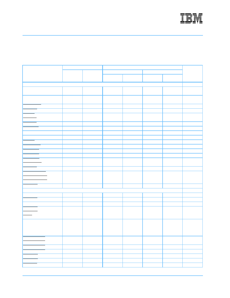
Preliminary
CPC710 PCI Bridge and Memory Controller Data Sheet
50
I/O Specifications--100 MHz
(Part 1 of 2)
Notes:
1. Output Valid from SYS_CLK
2. Output Hold from SYS_CLK
3. All inputs are referenced to the rising edge of SYS_CLK.
Signal
Input (ns)
Output (ns)
Notes
Setup
(T
IS
min)
Hold
(T
IH
min)
Valid
Hold
Max
Load
(pf)
Min
Load
(pf)
60x Bus Interface
SYS_ADDR0:31
SYS_ADDRP0:3
2.9
0
5.2
30
0.2
6
SYS_DATA0:63
SYS_DATP0:7
2.5
0.2
4.7
30
0.3
6
SYS_ARTRY
4.4
0.1
4.1
30
0.4
6
SYS_SHD
2.4
0
4.5
30
0.3
6
SYS_TA
SYS_TEA
3.3
0
4.5
30
0.3
6
SYS_TBE
nana4.5
30
0.3
6
SYS_TBST
2
0
5
25
0.6
5
SYS_TSIZ0:2
2.5
0.1
5
25
0.6
5
SYS_TT0:4
3.9
0
5
25
0.6
5
SYS_TS
3.9
0
4.5
30
0.3
6
SYS_L2_HIT
4.5
0.1
nananana
SYS_BR0:3
3.9
0
nananana
SYS_AACK
nana4.1
30
0.4
6
SYS_BG0:3
SYS_DBG0:3
nana5.2
15
0.5
6
SYS_GBL
nana 5
25
0.6
5
SYS_MACHK0:1
SYS_HRESET0:1
SYS_SRESET0:1
nana 5
25
0.6
5
CHKSTOP
nana6.6
25
1.6
5
SDRAM Interface
MDATA00:71
2
0.5
4.5
15
0.5
5
1, 2
SDCS0:11
nana4.6
30
1
15
1, 2
SDCKE0:9
nana4.6
30
1
15
1, 2
SDRAS0:1
SDCAS0:1
WE0:1
nana8.2
70
1, 2
MADDR13:1
MADDR0_ODD
MADDR0_EVEN
BS1:0
nana7.3
30
0.5
10
1, 2
MUX_CLKEN1B
MUX_CLKEN2B
nana5.2
35
0.5
10
1, 2
MUX_CLKENA1
nana5.8
35
0.5
10
1, 2
MUX_CLKENA2
nana4.9
35
0.5
10
1, 2
MUX_OEA
nana5.2
35
0.5
10
1, 2
MUX_OEB
nana5.4
35
0.5
10
1, 2
MUX_SEL
nana5.6
35
1
10
1, 2
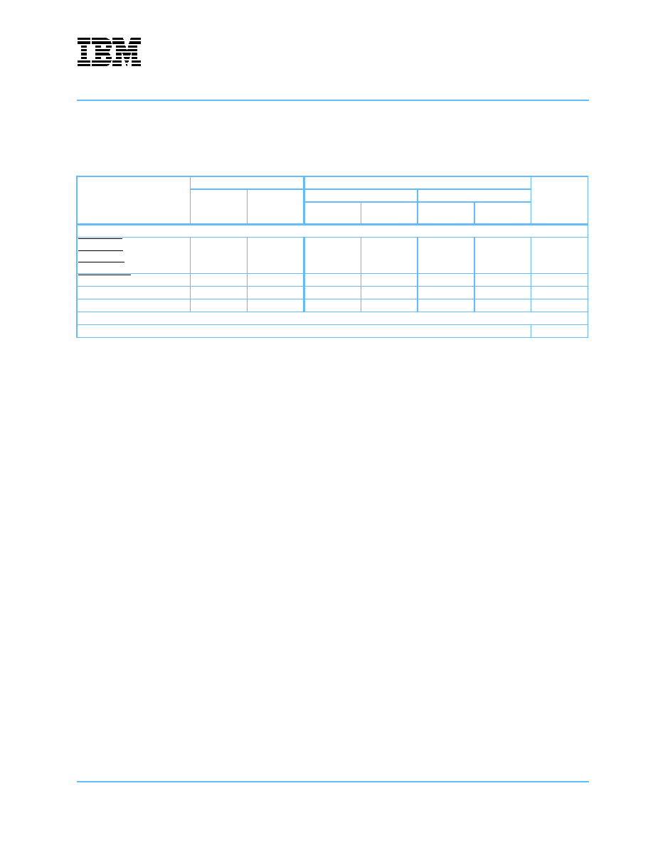
Preliminary
CPC710 PCI Bridge and Memory Controller Data Sheet
51
SIO Interface
FLASH_CE
FLASH_OE
FLASH_WE
nana8.1
80
0.8
5
1, 2
PRES_OE0:1
nana5.4
20
1
5
1, 2
XADR_LAT
nana6.9
25
1
5
1, 2
XCVR_RD
nana6.2
25
1
5
1, 2
Note: Refer to P_ADL31:0 signals in the PCI-32 section for FLASH address and data signal I/O timing.
PCI Interface (See "PCI I/O Specifications--133 MHz" on page 52)
I/O Specifications--100 MHz
(Part 2 of 2)
Notes:
1. Output Valid from SYS_CLK
2. Output Hold from SYS_CLK
3. All inputs are referenced to the rising edge of SYS_CLK.
Signal
Input (ns)
Output (ns)
Notes
Setup
(T
IS
min)
Hold
(T
IH
min)
Valid
Hold
Max
Load
(pf)
Min
Load
(pf)
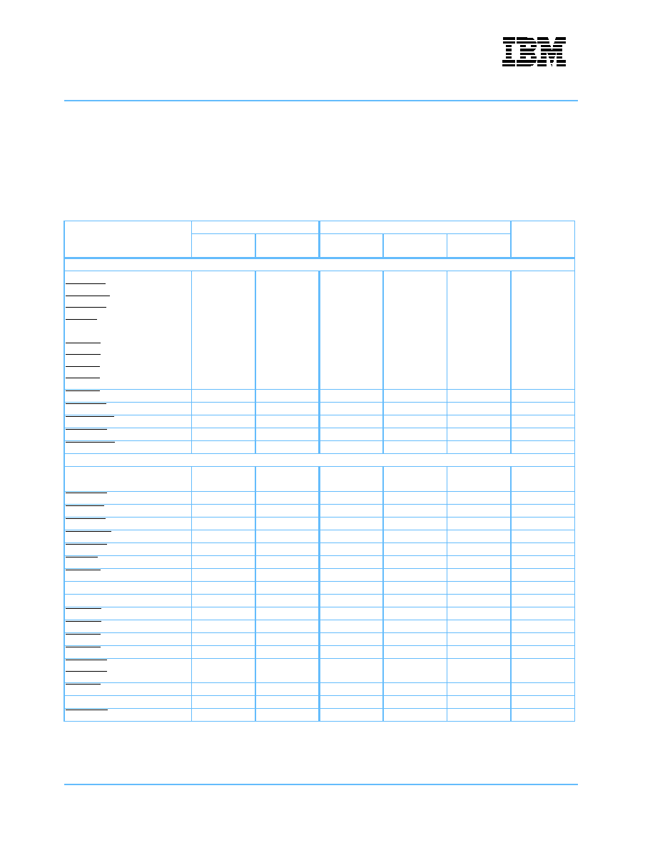
Preliminary
CPC710 PCI Bridge and Memory Controller Data Sheet
52
PCI I/O Specifications--133 MHz
Notes:
1. Output Valid from PCI_CLK
2. Input Setup to PCI_CLK
3. Input Hold from PCI_CLK
4. Output Valid from PCG_CLK
5. Input Setup to PCG_CLK
6. Input Hold from PCG_CLK
Signal
Input (ns)
Output Valid (ns)
Notes
Setup
(T
IS
min)
Hold
(T
IH
min)
Min
Max
Load (pf)
PCI-32 Interface @ 33 MHz
P_ADL31:00
P_CBE3:0
P_DEVSEL
P_FRAME
P_IRDY
P_PAR
P_PERR
P_SERR
P_STOP
P_TRDY
7
0.5
2.6
11
50
1, 2, 3
P_LOCK
nananana50
P_GNT0:3
nana3.2
12
50
1
P_MEMACK
nana4.4
5
30
1
P_REQ0:6
12
0.5
nanana2, 3
P_MEMREQ
nanananana2, 3
PCI-64 Interface @ 66 MHz
G_ADH31:0
G_ADL31:0
1.8
0
2
7.4
10
4, 5, 6
G_CBE7:0
3
0
2
6.9
10
4, 5, 6
G_ACK64
3.8
0
2
6.4
10
4, 5, 6
G_REQ64
2.1
0
2
7.2
10
4, 5, 6
G_DEVSEL
3.8
0
2
6
10
4, 5, 6
G_FRAME
3.4
0
2
6.4
10
4, 5, 6
G_IRDY
4.3
0
2
6
10
4, 5, 6
G_LOCK
nananana10
G_PAR
2.8
0
nana10
4, 5, 6
G_PAR64
2.1
0
2
6.6
10
4, 5, 6
G_PERR
1
0
2
6.3
10
4, 5, 6
G_SERR
1.8
0
2
6.5
10
4, 5, 6
G_STOP
3
0
2
6.6
10
4, 5, 6
G_TRDY
3.6
0
2
6.5
10
4, 5, 6
G_GNT0:2
G_GNT4:7
nana 2
6.4
10
4
G_GNT3
nana 2
6
10
4
G_IDSEL
1.8
0
nanana5, 6
G_REQ0:7
4.3
0
nanana5, 6

Preliminary
CPC710 PCI Bridge and Memory Controller Data Sheet
53
PCI I/O Specifications--100 MHz
Notes:
1. Output Valid from PCI_CLK
2. Input Setup to PCI_CLK
3. Input Hold from PCI_CLK
4. Output Valid from PCG_CLK
5. Input Setup to PCG_CLK
6. Input Hold from PCG_CLK
Signal
Input (ns)
Output Valid (ns)
Notes
Setup
(T
IS
min)
Hold
(T
IH
min)
Min
Max
Load (pf)
PCI-32 Interface @ 33 MHz
P_ADL31:00
P_CBE3:0
P_DEVSEL
P_FRAME
P_IRDY
P_PAR
P_PERR
P_SERR
P_STOP
P_TRDY
7
0.5
2
11.2
50
1, 2, 3
P_LOCK
nananana50
P_GNT0:3
nana 2
12.2
50
1
P_MEMACK
nanana11.2
50
1
P_REQ0:6
12
0.5
nanana2, 3
P_MEMREQ
nanananana2, 3
PCI-64 Interface @ 66 MHz
G_ADH31:0
G_ADL31:0
2
0
2
7.6
10
4, 5, 6
G_CBE7:0
3.2
0
2
7.1
10
4, 5, 6
G_ACK64
4
0
2
6.6
10
4, 5, 6
G_REQ64
2.3
0
2
7.4
10
4, 5, 6
G_DEVSEL
4
0
2
6.2
10
4, 5, 6
G_FRAME
3.6
0
2
6.6
10
4, 5, 6
G_IRDY
4.5
0
2
6.2
10
4, 5, 6
G_LOCK
nananana10
G_PAR
3
0
2
6.6
10
4, 5, 6
G_PAR64
2.3
0
2
6.8
10
4, 5, 6
G_PERR
1.2
0
2
6.5
10
4, 5, 6
G_SERR
2
0
2
6.7
10
4, 5, 6
G_STOP
3.2
0
2
6.8
10
4, 5, 6
G_TRDY
3.8
0
2
6.7
10
4, 5, 6
G_GNT0:2
G_GNT4:7
nana 2
6.6
10
4
G_GNT3
nana 2
6.2
10
4
G_IDSEL
2
0
nanana5, 6
G_REQ0:7
4.5
0
nanana5, 6

Preliminary
CPC710 PCI Bridge and Memory Controller Data Sheet
54
Copyright International Business Machines Corporation 2001, 2002
All Rights Reserved
Printed in the United States of America March 2002
The following are trademarks of International Business Machines Corporation in the United
States, or other countries, or both:
Other company, product, and service names may be trademarks or service marks of others.
Preliminary Edition (3/25/02)
This document contains information on a new product under development by IBM.
IBM reserves the right to change or discontinue this product without notice.
This document is a preliminary edition of the PCI Bridge and Memory Controller data sheet
.
Make sure you are using the correct edition for the
level of the product.
While the information contained herein is believed to be accurate, such information is
preliminary, and should not be relied upon for accuracy or completeness, and no
representations or warranties of accuracy or completeness are made.
All information contained in this document is subject to change without notice. The products
described in this document are NOT intended for use in implantation or other life support
applications where malfunction may result in injury or death to persons. The information
contained in this document does not affect or change IBM product specifications or
warranties. Nothing in this document shall operate as an express or implied license or
indemnity under the intellectual property rights of IBM or third parties. All information
contained in this document was obtained in specific environments, and is presented as an
illustration. The results obtained in other operating environments may vary.
THE INFORMATION CONTAINED IN THIS DOCUMENT IS PROVIDED ON AN "AS IS"
BASIS. In no event will IBM be liable for damages arising directly or indirectly from any use
of the information contained in this document.
IBM Microelectronics Division
1580 Route 52, Bldg. 504
Hopewell Junction, NY 12533-6351
The IBM home page can be found at www.ibm.com
The IBM Microelectronics Division home page can be found at www.chips.ibm.com
SA14-2572-05
IBM
IBM Logo
PowerPC