
IBM PowerNPTM
NP4GS3
Network Processor
Preliminary
January 29, 2003

0.1 Copyright and Disclaimer
Copyright International Business Machines Corporation 1999, 2003
All Rights Reserved
US Government Users Restricted Rights - Use, duplication or disclosure restricted by GSA ADP Schedule Contract with IBM Corp.
Printed in the United States of America January 2003
The following are trademarks of International Business Machines Corporation in the United States, or other countries, or
both.
IBM
IBM Logo
PowerPC
PowerNP
IEEE and IEEE 802 are registered trademarks of IEEE in all cases.
Other company, product and service names may be trademarks or service marks of others.
All information contained in this document is subject to change without notice. The products described in this document
are NOT intended for use in applications such as implantation, life support, or other hazardous uses where malfunction
could result in death, bodily injury, or catastrophic property damage. The information contained in this document does not
affect or change IBM product specifications or warranties. Nothing in this document shall operate as an express or implied
license or indemnity under the intellectual property rights of IBM or third parties. All information contained in this docu-
ment was obtained in specific environments, and is presented as an illustration. The results obtained in other operating
environments may vary.
While the information contained herein is believed to be accurate, such information is preliminary, and should not be
relied upon for accuracy or completeness, and no representations or warranties of accuracy or completeness are made.
THE INFORMATION CONTAINED IN THIS DOCUMENT IS PROVIDED ON AN "AS IS" BASIS. In no event will IBM be
liable for damages arising directly or indirectly from any use of the information contained in this document.
IBM Microelectronics Division
2070 Route 52, Bldg. 330
Hopewell Junction, NY 12533-6351
The IBM home page can be found at
http://www.ibm.com
The IBM Microelectronics Division home page
can be found at http://www.ibm.com/chips
np3_DS_title.fm.11
January 29, 2003
Note: This document contains information on products in the sampling and/or initial production phases of
development. This information is subject to change without notice. Verify with your IBM field applications engi-
neer that you have the latest version of this document before finalizing a design.

IBM PowerNP NP4GS3
Preliminary
Network Processor
np3_ds_TOC.fm.11
January 29, 2003
Contents
Page 3 of 605
Contents
About This Book ........................................................................................................... 25
Who Should Read This Manual ............................................................................................................ 25
Related Publications ............................................................................................................................. 25
Conventions Used in This Manual ........................................................................................................ 25
1. General Information .................................................................................................. 27
1.1 Features .......................................................................................................................................... 27
1.2 Ordering Information ....................................................................................................................... 28
1.3 Overview ......................................................................................................................................... 29
1.4 NP4GS3-Based Systems ................................................................................................................ 29
1.5 Structure .......................................................................................................................................... 31
1.5.1 EPC Structure ........................................................................................................................ 32
1.5.1.1 Coprocessors ................................................................................................................. 33
1.5.1.2 Enhanced Threads ......................................................................................................... 33
1.5.1.3 Hardware Accelerators ................................................................................................... 34
1.5.2 NP4GS3 Memory .................................................................................................................. 34
1.6 Data Flow ........................................................................................................................................ 35
1.6.1 Basic Data Flow ..................................................................................................................... 35
1.6.2 Data Flow in the EPC ............................................................................................................ 36
2. Physical Description ................................................................................................. 39
2.1 Pin Information ................................................................................................................................ 40
2.1.1 Packet Routing Switch Interface Pins .................................................................................... 41
2.1.2 Flow Control Interface Pins ................................................................................................... 43
2.1.3 ZBT Interface Pins ................................................................................................................. 44
2.1.4 DDR DRAM Interface Pins .................................................................................................... 46
2.1.4.1 D3, D2, D1, and D0 Interface Pins ................................................................................. 52
2.1.4.2 D4_0 and D4_1 Interface Pins ....................................................................................... 54
2.1.4.3 D6_x Interface Pins ........................................................................................................ 55
2.1.4.4 DS1 and DS0 Interface Pins .......................................................................................... 56
2.1.5 PMM Interface Pins ............................................................................................................... 58
2.1.5.1 TBI Bus Pins ................................................................................................................... 61
2.1.5.2 GMII Bus Pins ................................................................................................................ 65
2.1.5.3 SMII Bus Pins ................................................................................................................. 67
2.1.5.4 POS Bus Pins ................................................................................................................. 69
2.1.6 PCI Pins ................................................................................................................................. 74
2.1.7 Management Bus Interface Pins ........................................................................................... 77
2.1.8 Miscellaneous Pins ................................................................................................................ 79
2.1.9 PLL Filter Circuit .................................................................................................................... 82
2.1.10 Thermal I/O Usage .............................................................................................................. 82
2.1.10.1 Temperature Calculation .............................................................................................. 83
2.1.10.2 Measurement Calibration ............................................................................................. 83
2.2 Clocking Domains ........................................................................................................................... 84
2.3 Mechanical Specifications ............................................................................................................... 86
2.4 IEEE 1149 (JTAG) Compliance ...................................................................................................... 88
2.4.1 Statement of JTAG Compliance ............................................................................................ 88

IBM PowerNP NP4GS3
Network Processor
Preliminary
Contents
Page 4 of 605
np3_ds_TOC.fm.11
January 29, 2003
2.4.2 JTAG Compliance Mode ........................................................................................................ 88
2.4.3 JTAG Implementation Specifics ............................................................................................. 88
2.4.4 Brief Overview of JTAG Instructions ...................................................................................... 89
2.5 Signal Pin Lists ................................................................................................................................ 90
3. Physical MAC Multiplexer ....................................................................................... 113
3.1 Ethernet Overview ......................................................................................................................... 114
3.1.1 Ethernet Interface Timing Diagrams .................................................................................... 115
3.1.2 Ethernet Counters ................................................................................................................ 117
3.1.3 Ethernet Support .................................................................................................................. 122
3.2 POS Overview ............................................................................................................................... 123
3.2.1 POS Timing Diagrams ......................................................................................................... 125
3.2.2 POS Counters ...................................................................................................................... 129
3.2.3 POS Support ........................................................................................................................ 133
4. Ingress Enqueuer / Dequeuer / Scheduler ............................................................ 135
4.1 Overview ....................................................................................................................................... 135
4.2 Operation ....................................................................................................................................... 136
4.2.1 Operational Details .............................................................................................................. 138
4.3 Ingress Flow Control ..................................................................................................................... 140
4.3.1 Flow Control Hardware Facilities ......................................................................................... 140
4.3.2 Hardware Function ............................................................................................................... 142
4.3.2.1 Exponentially Weighted Moving Average (EWMA) ...................................................... 142
4.3.2.2 Flow Control Hardware Actions .................................................................................... 142
5. Switch Interface ....................................................................................................... 143
5.1 Ingress Switch Data Mover ........................................................................................................... 145
5.1.1 Cell Header .......................................................................................................................... 146
5.1.2 Frame Header ...................................................................................................................... 149
5.2 Ingress Switch Cell Interface ......................................................................................................... 152
5.2.1 Idle Cell Format .................................................................................................................... 152
5.2.1.1 CRC Bytes: Word 15 .................................................................................................... 153
5.2.1.2 I-SCI Transmit Header for the Idle Cell ........................................................................ 153
5.2.2 Switch Data Cell Format - Ingress and Egress .................................................................... 154
5.3 Data-Aligned Synchronous Link Interface ..................................................................................... 155
5.4 Egress Switch Cell Interface ......................................................................................................... 156
5.4.1 Master and Multicast Grant Reporting ................................................................................. 156
5.4.2 Output Queue Grant Reporting ............................................................................................ 156
5.4.2.1 OQG Reporting in External Wrap Mode ....................................................................... 157
5.4.3 Switch Fabric to Network Processor Egress Idle Cell .......................................................... 159
5.4.4 Receive Header Formats for Sync Cells .............................................................................. 162
5.5 Egress Switch Data Mover ............................................................................................................ 162
5.6 IBM Packet Routing Switch PRS28.4G Configuration Notes ........................................................ 162
6. Egress Enqueuer / Dequeuer / Scheduler ............................................................. 163
6.1 Functional Blocks .......................................................................................................................... 164
6.2 Operation ....................................................................................................................................... 166
6.3 Egress Flow Control ...................................................................................................................... 169

IBM PowerNP NP4GS3
Preliminary
Network Processor
np3_ds_TOC.fm.11
January 29, 2003
Contents
Page 5 of 605
6.3.1 Flow Control Hardware Facilities ......................................................................................... 169
6.3.2 Remote Egress Status Bus ................................................................................................. 171
6.3.2.1 Bus Sequence and Timing ........................................................................................... 171
6.3.2.2 Configuration ................................................................................................................ 173
6.3.3 Hardware Function .............................................................................................................. 175
6.3.3.1 Exponentially Weighted Moving Average ..................................................................... 175
6.3.3.2 Flow Control Hardware Actions .................................................................................... 176
6.4 The Egress Scheduler ................................................................................................................... 177
6.4.1 Egress Scheduler Components ........................................................................................... 179
6.4.1.1 Scheduling Calendars .................................................................................................. 179
6.4.1.2 Flow Queues ................................................................................................................ 180
6.4.1.3 Target Port Queues ...................................................................................................... 182
6.4.2 Configuring Flow Queues .................................................................................................... 183
6.4.2.1 Additional Configuration Notes ..................................................................................... 183
6.4.3 Scheduler Accuracy and Capacities .................................................................................... 183
7. Embedded Processor Complex ............................................................................. 185
7.1 Overview ....................................................................................................................................... 185
7.1.1 Thread Types ...................................................................................................................... 189
7.2 Dyadic Protocol Processor Unit (DPPU) ....................................................................................... 190
7.2.1 Core Language Processor (CLP) ........................................................................................ 191
7.2.1.1 Core Language Processor Address Map ..................................................................... 193
7.2.2 CLP Opcode Formats .......................................................................................................... 195
7.2.3 DPPU Coprocessors ........................................................................................................... 195
7.2.4 Shared Memory Pool ........................................................................................................... 196
7.3 CLP Opcode Formats ................................................................................................................... 197
7.3.1 Control Opcodes .................................................................................................................. 197
7.3.1.1 Nop Opcode ................................................................................................................. 198
7.3.1.2 Exit Opcode .................................................................................................................. 198
7.3.1.3 Test and Branch Opcode ............................................................................................. 198
7.3.1.4 Branch and Link Opcode .............................................................................................. 199
7.3.1.5 Return Opcode ............................................................................................................. 200
7.3.1.6 Branch Register Opcode .............................................................................................. 200
7.3.1.7 Branch PC Relative Opcode ........................................................................................ 200
7.3.1.8 Branch Reg+Off Opcode .............................................................................................. 201
7.3.2 Data Movement Opcodes .................................................................................................... 202
7.3.2.1 Memory Indirect Opcode .............................................................................................. 206
7.3.2.2 Memory Address Indirect Opcode ................................................................................ 207
7.3.2.3 Memory Direct Opcode ................................................................................................ 208
7.3.2.4 Scalar Access Opcode ................................................................................................. 208
7.3.2.5 Scalar Immediate Opcode ............................................................................................ 209
7.3.2.6 Transfer Quadword Opcode ......................................................................................... 209
7.3.2.7 Zero Array Opcode ....................................................................................................... 210
7.3.3 Coprocessor Execution Opcodes ........................................................................................ 211
7.3.3.1 Execute Direct Opcode ................................................................................................ 212
7.3.3.2 Execute Indirect Opcode .............................................................................................. 213
7.3.3.3 Execute Direct Conditional Opcode ............................................................................. 213
7.3.3.4 Execute Indirect Conditional Opcode ........................................................................... 214
7.3.3.5 Wait Opcode ................................................................................................................. 214
7.3.3.6 Wait and Branch Opcode ............................................................................................. 215

IBM PowerNP NP4GS3
Network Processor
Preliminary
Contents
Page 6 of 605
np3_ds_TOC.fm.11
January 29, 2003
7.3.4 ALU Opcodes ....................................................................................................................... 216
7.3.4.1 Arithmetic Immediate Opcode ...................................................................................... 216
7.3.4.2 Logical Immediate Opcode ........................................................................................... 219
7.3.4.3 Compare Immediate Opcode ....................................................................................... 219
7.3.4.4 Load Immediate Opcode .............................................................................................. 220
7.3.4.5 Arithmetic Register Opcode .......................................................................................... 223
7.3.4.6 Count Leading Zeros Opcode ...................................................................................... 225
7.4 DPPU Coprocessors ..................................................................................................................... 226
7.4.1 Tree Search Engine Coprocessor ........................................................................................ 227
7.4.2 Data Store Coprocessor ...................................................................................................... 227
7.4.2.1 Data Store Coprocessor Address Map ......................................................................... 228
7.4.2.2 Data Store Coprocessor Commands ............................................................................ 234
7.4.3 Control Access Bus (CAB) Coprocessor ............................................................................. 244
7.4.3.1 CAB Coprocessor Address Map ................................................................................... 244
7.4.3.2 CAB Access to NP4GS3 Structures ............................................................................. 245
7.4.3.3 CAB Coprocessor Commands ..................................................................................... 246
7.4.4 Enqueue Coprocessor ......................................................................................................... 247
7.4.4.1 Enqueue Coprocessor Address Map ............................................................................ 248
7.4.4.2 Enqueue Coprocessor Commands .............................................................................. 260
7.4.5 Checksum Coprocessor ....................................................................................................... 266
7.4.5.1 Checksum Coprocessor Address Map ......................................................................... 266
7.4.5.2 Checksum Coprocessor Commands ............................................................................ 267
7.4.6 String Copy Coprocessor ..................................................................................................... 271
7.4.6.1 String Copy Coprocessor Address Map ....................................................................... 271
7.4.6.2 String Copy Coprocessor Commands .......................................................................... 271
7.4.7 Policy Coprocessor .............................................................................................................. 272
7.4.7.1 Policy Coprocessor Address Map ................................................................................ 272
7.4.7.2 Policy Coprocessor Commands ................................................................................... 272
7.4.8 Counter Coprocessor ........................................................................................................... 273
7.4.8.1 Counter Coprocessor Address Map ............................................................................. 273
7.4.8.2 Counter Coprocessor Commands ................................................................................ 274
7.4.9 Coprocessor Response Bus ................................................................................................ 277
7.4.9.1 Coprocessor Response Bus Address Map ................................................................... 277
7.4.9.2 Coprocessor Response Bus Commands ..................................................................... 277
7.4.9.3 14-bit Coprocessor Response Bus ............................................................................... 278
7.4.10 Semaphore Coprocessor ................................................................................................... 278
7.4.10.1 Semaphore Coprocessor Commands ........................................................................ 278
7.4.10.2 Error Conditions .......................................................................................................... 280
7.4.10.3 Software Use Models ................................................................................................. 281
7.5 Interrupts and Timers .................................................................................................................... 282
7.5.1 Interrupts .............................................................................................................................. 282
7.5.1.1 Interrupt Vector Registers ............................................................................................. 282
7.5.1.2 Interrupt Mask Registers .............................................................................................. 282
7.5.1.3 Interrupt Target Registers ............................................................................................. 282
7.5.1.4 Software Interrupt Registers ......................................................................................... 282
7.5.2 Timers .................................................................................................................................. 283
7.5.2.1 Timer Interrupt Counters .............................................................................................. 283
7.6 Dispatch Unit ................................................................................................................................. 284
7.6.1 Port Configuration Memory .................................................................................................. 286
7.6.1.1 Port Configuration Memory Index Definition ................................................................. 286

IBM PowerNP NP4GS3
Preliminary
Network Processor
np3_ds_TOC.fm.11
January 29, 2003
Contents
Page 7 of 605
7.6.2 Port Configuration Memory Contents Definition .................................................................. 287
7.6.3 Completion Unit ................................................................................................................... 288
7.7 Hardware Classifier ....................................................................................................................... 289
7.7.1 Ingress Classification ........................................................................................................... 289
7.7.1.1 Ingress Classification Input .......................................................................................... 289
7.7.1.2 Ingress Classification Output ........................................................................................ 290
7.7.2 Egress Classification ........................................................................................................... 294
7.7.2.1 Egress Classification Input ........................................................................................... 294
7.7.2.2 Egress Classification Output ........................................................................................ 295
7.7.3 Completion Unit Label Generation ...................................................................................... 296
7.8 Policy Manager ............................................................................................................................. 297
7.9 Counter Manager .......................................................................................................................... 300
7.9.1 Counter Manager Usage ..................................................................................................... 302
7.10 Semaphore Manager .................................................................................................................. 308
8. Tree Search Engine ................................................................................................ 311
8.1 Overview ....................................................................................................................................... 311
8.1.1 Addressing Control Store (CS) ............................................................................................ 311
8.1.2 D6 Control Store. ................................................................................................................. 312
8.1.3 Logical Memory Views of D6 ............................................................................................... 312
8.1.4 Control Store Use Restrictions ............................................................................................ 313
8.1.5 Object Shapes ..................................................................................................................... 314
8.1.6 Illegal Memory Access ......................................................................................................... 316
8.1.7 Memory Range Checking (Address Bounds Check) ........................................................... 317
8.2 Trees and Tree Searches ............................................................................................................. 318
8.2.1 Input Key and Color Register for FM and LPM Trees ......................................................... 319
8.2.2 Input Key and Color Register for SMT Trees ...................................................................... 319
8.2.3 Direct Table ......................................................................................................................... 320
8.2.3.1 Pattern Search Control Blocks (PSCB) ........................................................................ 320
8.2.3.2 Leaves and Compare-at-End Operation ...................................................................... 321
8.2.3.3 Cascade/Cache ............................................................................................................ 321
8.2.3.4 Cache Flag and NrPSCBs Registers ........................................................................... 321
8.2.3.5 Cache Management ..................................................................................................... 322
8.2.3.6 Search Output .............................................................................................................. 322
8.2.4 Tree Search Algorithms ....................................................................................................... 322
8.2.4.1 FM Trees ...................................................................................................................... 322
8.2.4.2 LPM Trees .................................................................................................................... 323
8.2.4.3 LPM PSCB Structure in Memory .................................................................................. 323
8.2.4.4 LPM Compact PSCB Support ...................................................................................... 324
8.2.4.5 LPM Trees with Multibit Compare ................................................................................ 326
8.2.4.6 SMT Trees .................................................................................................................... 329
8.2.4.7 Compare-at-End Operation .......................................................................................... 330
8.2.4.8 Ropes ........................................................................................................................... 331
8.2.4.9 Aging ............................................................................................................................ 332
8.2.5 Tree Configuration and Initialization .................................................................................... 333
8.2.5.1 The LUDefTable ........................................................................................................... 333
8.2.5.2 TSE Free Lists (TSE_FL) ............................................................................................. 336
8.2.6 TSE Registers and Register Map ........................................................................................ 337
8.2.7 TSE Instructions .................................................................................................................. 342
8.2.7.1 FM Tree Search (TS_FM) ............................................................................................ 343

IBM PowerNP NP4GS3
Network Processor
Preliminary
Contents
Page 8 of 605
np3_ds_TOC.fm.11
January 29, 2003
8.2.7.2 LPM Tree Search (TS_LPM) ........................................................................................ 344
8.2.7.3 SMT Tree Search (TS_SMT) ........................................................................................ 346
8.2.7.4 Memory Read (MRD) ................................................................................................... 347
8.2.7.5 Memory Write (MWR) ................................................................................................... 348
8.2.7.6 Hash Key (HK) .............................................................................................................. 349
8.2.7.7 Read LUDefTable (RDLUDEF) .................................................................................... 350
8.2.7.8 Compare-at-End (COMPEND) ..................................................................................... 352
8.2.7.9 DistinguishPosition for Fast Table Update (DISTPOS_GDH) ...................................... 353
8.2.7.10 Read PSCB for Fast Table Update (RDPSCB_GDH) ................................................ 354
8.2.7.11 Write PSCB for Fast Table Update (WRPSCB_GDH) ............................................... 356
8.2.7.12 SetPatBit_GDH ........................................................................................................... 357
8.2.8 GTH Hardware Assist Instructions ....................................................................................... 359
8.2.8.1 Hash Key GTH (HK_GTH) ........................................................................................... 360
8.2.8.2 Read LUDefTable GTH (RDLUDEF GTH) ................................................................... 360
8.2.8.3 Tree Search Enqueue Free List (TSENQFL) ............................................................... 361
8.2.8.4 Tree Search Dequeue Free List (TSDQFL) .................................................................. 362
8.2.8.5 Read Current Leaf from Rope (RCLR) ......................................................................... 362
8.2.8.6 Advance Rope with Optional Delete Leaf (ARDL) ........................................................ 363
8.2.8.7 Tree Leaf Insert Rope (TLIR) ....................................................................................... 364
8.2.8.8 Clear PSCB (CLRPSCB) .............................................................................................. 364
8.2.8.9 Read PSCB (RDPSCB) ................................................................................................ 365
8.2.8.10 Write PSCB (WRPSCB) ............................................................................................. 365
8.2.8.11 Push PSCB (PUSHPSCB) ......................................................................................... 367
8.2.8.12 Distinguish (DISTPOS) ............................................................................................... 367
8.2.8.13 TSR0 Pattern (TSR0PAT) .......................................................................................... 368
8.2.8.14 Pattern 2DTA (PAT2DTA) .......................................................................................... 368
8.2.9 Hash Functions .................................................................................................................... 369
9. Serial / Parallel Manager Interface ......................................................................... 377
9.1 SPM Interface Components .......................................................................................................... 377
9.2 SPM Interface Data Flow .............................................................................................................. 378
9.3 SPM Interface Protocol ................................................................................................................. 380
9.4 SPM CAB Address Space ............................................................................................................. 382
9.4.1 Byte Access Space .............................................................................................................. 382
9.4.2 Word Access Space ............................................................................................................. 382
9.4.3 EEPROM Access Space ...................................................................................................... 383
9.4.3.1 EEPROM Single-Byte Access ...................................................................................... 383
9.4.3.2 EEPROM 2-Byte Access .............................................................................................. 384
9.4.3.3 EEPROM 3-Byte Access .............................................................................................. 384
9.4.3.4 EEPROM 4-Byte Access .............................................................................................. 385
10. Embedded PowerPCTM Subsystem ...................................................................... 387
10.1 Description .................................................................................................................................. 387
10.2 Processor Local Bus and Device Control Register Buses .......................................................... 389
10.2.1 Processor Local Bus (PLB) ................................................................................................ 389
10.2.2 Device Control Register (DCR) Bus ................................................................................... 390
10.3 PLB Address Map ....................................................................................................................... 391
10.4 CAB Address Map ....................................................................................................................... 393
10.5 Universal Interrupt Controller (UIC) Macro .................................................................................. 394

IBM PowerNP NP4GS3
Preliminary
Network Processor
np3_ds_TOC.fm.11
January 29, 2003
Contents
Page 9 of 605
10.6 PCI/PLB Bridge Macro ................................................................................................................ 395
10.7 CAB Interface Macro ................................................................................................................... 399
10.7.1 PowerPC CAB Address (PwrPC_CAB_Addr) Register ..................................................... 401
10.7.2 PowerPC CAB Data (PwrPC_CAB_Data) Register .......................................................... 401
10.7.3 PowerPC CAB Control (PwrPC_CAB_Cntl) Register ........................................................ 402
10.7.4 PowerPC CAB Status (PwrPC_CAB_Status) Register ..................................................... 402
10.7.5 PowerPC CAB Mask (PwrPC_CAB_Mask) Register ........................................................ 403
10.7.6 PowerPC CAB Write Under Mask Data (PwrPC_CAB_WUM_Data) ................................ 404
10.7.7 PCI Host CAB Address (Host_CAB_Addr) Register ......................................................... 404
10.7.8 PCI Host CAB Data (Host_CAB_Data) Register ............................................................... 405
10.7.9 PCI Host CAB Control (Host_CAB_Cntl) Register ............................................................ 405
10.7.10 PCI Host CAB Status (Host_CAB_Status) Register ........................................................ 406
10.7.11 PCI Host CAB Mask (Host_CAB_Mask) Register ........................................................... 406
10.7.12 PCI Host CAB Write Under Mask Data (Host_CAB_WUM_Data) Register .................... 407
10.8 Mailbox Communications and DRAM Interface Macro ............................................................... 408
10.8.1 Mailbox Communications Between PCI Host and PowerPC Subsystem .......................... 409
10.8.2 PCI Interrupt Status (PCI_Interr_Status) Register ............................................................. 411
10.8.3 PCI Interrupt Enable (PCI_Interr_Ena) Register ............................................................... 412
10.8.4 PowerPC Subsystem to PCI Host Message Resource (P2H_Msg_Resource) Register .. 413
10.8.5 PowerPC Subsystem to Host Message Address (P2H_Msg_Addr) Register ................... 413
10.8.6 PowerPC Subsystem to Host Doorbell (P2H_Doorbell) Register ...................................... 414
10.8.7 Host to PowerPC Subsystem Message Address (H2P_Msg_Addr) Register ................... 415
10.8.8 Host to PowerPC Subsystem Doorbell (H2P_Doorbell) Register ...................................... 416
10.8.9 Mailbox Communications Between PowerPC Subsystem and EPC ................................. 417
10.8.10 EPC to PowerPC Subsystem Resource (E2P_Msg_Resource) Register ....................... 417
10.8.11 EPC to PowerPC Subsystem Message Address (E2P_Msg_Addr) Register ................. 419
10.8.12 EPC to PowerPC Subsystem Doorbell (E2P_Doorbell) Register .................................... 420
10.8.13 EPC Interrupt Vector Register ......................................................................................... 421
10.8.14 EPC Interrupt Mask Register ........................................................................................... 421
10.8.15 PowerPC Subsystem to EPC Message Address (P2E_Msg_Addr) Register ................. 422
10.8.16 PowerPC Subsystem to EPC Doorbell (P2E_Doorbell) Register .................................... 423
10.8.17 Mailbox Communications Between PCI Host and EPC ................................................... 424
10.8.18 EPC to PCI Host Resource (E2H_Msg_Resource) Register .......................................... 425
10.8.19 EPC to PCI Host Message Address (E2H_Msg_Addr) Register ..................................... 426
10.8.20 EPC to PCI Host Doorbell (E2H_Doorbell) Register ....................................................... 427
10.8.21 PCI Host to EPC Message Address (H2E_Msg_Addr) Register ..................................... 429
10.8.22 PCI Host to EPC Doorbell (H2E_Doorbell) Register ....................................................... 430
10.8.23 Message Status (Msg_Status) Register .......................................................................... 431
10.8.24 PowerPC Boot Redirection Instruction Registers (Boot_Redir_Inst) ............................... 433
10.8.25 PowerPC Machine Check (PwrPC_Mach_Chk) Register ............................................... 434
10.8.26 Parity Error Status and Reporting .................................................................................... 434
10.8.27 Slave Error Address Register (SEAR) ............................................................................. 435
10.8.28 Slave Error Status Register (SESR) ................................................................................ 436
10.8.29 Parity Error Counter (Perr_Count) Register .................................................................... 437
10.9 System Start-Up and Initialization ............................................................................................... 438
10.9.1 NP4GS3 Resets ................................................................................................................ 438
10.9.2 Systems Initialized by External PCI Host Processors ....................................................... 439
10.9.3 Systems with PCI Host Processors and Initialized by PowerPC Subsystem .................... 440
10.9.4 Systems Without PCI Host Processors and Initialized by PowerPC Subsystem .............. 441
10.9.5 Systems Without PCI Host or Delayed PCI Configuration and Initialized by EPC ............ 442

IBM PowerNP NP4GS3
Network Processor
Preliminary
Contents
Page 10 of 605
np3_ds_TOC.fm.11
January 29, 2003
11. Reset and Initialization .......................................................................................... 443
11.1 Overview ..................................................................................................................................... 443
11.2 Step 1: Set I/Os ........................................................................................................................... 445
11.3 Step 2: Reset the NP4GS3 ......................................................................................................... 446
11.4 Step 3: Boot ................................................................................................................................. 447
11.4.1 Boot the Embedded Processor Complex (EPC) ................................................................ 447
11.4.2 Boot the PowerPC Processor ............................................................................................ 447
11.4.3 Boot Summary ................................................................................................................... 447
11.5 Step 4: Setup 1 ............................................................................................................................ 448
11.6 Step 5: Diagnostics 1 .................................................................................................................. 449
11.7 Step 6: Setup 2 ............................................................................................................................ 450
11.8 Step 7: Hardware Initialization ..................................................................................................... 451
11.9 Step 8: Diagnostics 2 .................................................................................................................. 452
11.10 Step 9: Operational ................................................................................................................... 453
11.11 Step 10: Configure .................................................................................................................... 454
11.12 Step 11: Initialization Complete ................................................................................................. 456
12. Debug Facilities ..................................................................................................... 457
12.1 Debugging Picoprocessors ......................................................................................................... 457
12.1.1 Single Step ......................................................................................................................... 457
12.1.2 Break Points ....................................................................................................................... 457
12.1.3 CAB Accessible Registers ................................................................................................. 457
12.2 RISCWatch .................................................................................................................................. 458
13. Configuration ......................................................................................................... 459
13.1 Memory Configuration ................................................................................................................. 459
13.1.1 Memory Configuration Register (Memory_Config) ............................................................ 460
13.1.2 DRAM Parameter Register (DRAM_Parm) ....................................................................... 462
13.1.3 Delay Calibration Registers (NP4GS3C (R3.x)) ................................................................ 467
13.2 Master Grant Mode Register (MG_Mode) ................................................................................... 472
13.3 TB Mode Register (TB_Mode) .................................................................................................... 473
13.3.1 Toggle Mode ...................................................................................................................... 475
13.3.1.1 DSU information ......................................................................................................... 475
13.3.1.2 ENQE Command and Qclass 5 or 6 ........................................................................... 476
13.4 Egress Reassembly Sequence Check Register (E_Reassembly_Seq_Ck) ............................... 477
13.5 Aborted Frame Reassembly Action Control Register (AFRAC) ................................................. 478
13.6 Packing Registers ....................................................................................................................... 479
13.6.1 Packing Control Register (Pack_Ctrl) ................................................................................ 479
13.6.2 Packing Delay Register (Pack_Dly) (NP4GS3B (R2.0)) .................................................... 480
13.7 Initialization Control Registers ..................................................................................................... 481
13.7.1 Initialization Register (Init) ................................................................................................. 481
13.7.2 Initialization Done Register (Init_Done) ............................................................................ 482
13.8 NP4GS3 Ready Register (NPR_Ready) .................................................................................... 483
13.9 Phase-Locked Loop Registers .................................................................................................... 484
13.9.1 Phase-Locked Loop Fail Register (PLL_Lock_Fail) ........................................................... 484
13.10 Software Controlled Reset Register (Soft_Reset) .................................................................... 485
13.11 Ingress Free Queue Threshold Configuration ........................................................................... 486

IBM PowerNP NP4GS3
Preliminary
Network Processor
np3_ds_TOC.fm.11
January 29, 2003
Contents
Page 11 of 605
13.11.1 BCB_FQ Threshold Registers ......................................................................................... 486
13.11.2 BCB_FQ Threshold for Guided Traffic (BCB_FQ_Th_GT) ............................................. 486
13.11.3 BCB_FQ_Threshold_0 Register (BCB_FQ_TH_0) ......................................................... 487
13.11.4 BCB_FQ_Threshold_1 Register (BCB_FQ_TH_1) ......................................................... 488
13.11.5 BCB_FQ_Threshold_2 Register (BCB_FQ_Th_2) .......................................................... 489
13.12 I-GDQ Threshold Register (I-GDQ_Th) (NP4GS3C (R3.x)) ..................................................... 490
13.13 Ingress Target DMU Data Storage Map Register (I_TDMU_DSU) .......................................... 491
13.14 Embedded Processor Complex Configuration .......................................................................... 492
13.14.1 PowerPC Core Reset Register (PowerPC_Reset) .......................................................... 492
13.14.2 PowerPC Boot Redirection Instruction Registers (Boot_Redir_Inst) ............................... 493
13.14.3 Watch Dog Reset Enable Register (WD_Reset_Ena) ..................................................... 494
13.14.4 Boot Override Register (Boot_Override) ......................................................................... 495
13.14.5 Thread Enable Register (Thread_Enable) ...................................................................... 496
13.14.6 GFH Data Disable Register (GFH_Data_Dis) ................................................................. 497
13.14.7 Ingress Maximum DCB Entries (I_Max_DCB) ................................................................. 498
13.14.8 Egress Maximum DCB Entries (E_Max_DCB) ................................................................ 499
13.14.9 My Target Blade Address Register (My_TB) ................................................................... 500
13.14.10 Local Target Blade Vector Register (Local_TB_Vector) ................................................ 501
13.14.11 Local MCTarget Blade Vector Register (Local_MC_TB_Max) ...................................... 502
13.14.12 Ordered Semaphore Enable Register (Ordered_Sem_Ena) ......................................... 503
13.14.13 Enhanced Classification Enable Register (Enh_HWC_Ena) (NP4GS3C (R3.x)) .......... 504
13.15 Flow Control Structures ............................................................................................................. 505
13.15.1 Ingress Flow Control Hardware Structures ...................................................................... 505
13.15.1.1 Ingress Transmit Probability Memory Register (I_Tx_Prob_Mem) .......................... 505
13.15.1.2 Ingress pseudorandom Number Register (I_Rand_Num) ........................................ 506
13.15.1.3 Free Queue Thresholds Register (FQ_Th) .............................................................. 507
13.15.2 Egress Flow Control Structures ....................................................................................... 508
13.15.2.1 Egress Transmit Probability Memory (E_Tx_Prob_Mem) Register .......................... 508
13.15.2.2 Egress pseudorandom Number (E_Rand_Num) ..................................................... 509
13.15.2.3 P0 Twin Count Threshold (P0_Twin_Th) ................................................................. 510
13.15.2.4 P1 Twin Count Threshold (P1_Twin_Th) ................................................................. 510
13.15.2.5 Egress P0 Twin Count EWMA Threshold Register (E_P0_Twin_EWMA_Th) ......... 511
13.15.2.6 Egress P1 Twin Count EWMA Threshold Register (E_P1_Twin_EWMA_Th) ......... 511
13.15.3 Exponentially Weighted Moving Average Constant (K) Register (EWMA_K) ................. 512
13.15.4 Exponentially Weighted Moving Average Sample Period (T) Register (EWMA_T) ......... 513
13.15.5 Flow Control Force Discard Register (FC_Force_Discard) (NP4GS3B (R2.0)) .............. 514
13.15.6 Remote Egress Status Bus Configuration Enables (RES_Data_Cnf) ............................. 515
13.16 Target Port Data Storage Map (TP_DS_MAP) Register .......................................................... 518
13.17 Egress SDM Stack Threshold Register (E_SDM_Stack_Th) ................................................... 521
13.18 Free Queue Extended Stack Maximum Size (FQ_ES_Max) Register ..................................... 522
13.19 Egress Free Queue Thresholds ................................................................................................ 523
13.19.1 FQ_ES_Threshold_0 Register (FQ_ES_Th_0) .............................................................. 523
13.19.2 FQ_ES_Threshold_1 Register (FQ_ES_Th_1) .............................................................. 524
13.19.3 FQ_ES_Threshold_2 Register (FQ_ES_Th_2) .............................................................. 524
13.20 Egress Frame Data Queue Thresholds (E_GRx_GBx_th) (NP4GS3C (R3.x)) ........................ 525
13.21 Discard Flow QCB Register (Discard_QCB) ............................................................................. 527
13.22 Bandwidth Allocation Register (BW_Alloc_Reg) (NP4GS3B (R2.0)) ........................................ 528
13.23 Miscellaneous Controls Register (MISC_CNTRL) (NP4GS3C (R3.x)) ..................................... 529
13.24 Frame Control Block FQ Size Register (FCB_FQ_Max) .......................................................... 530

IBM PowerNP NP4GS3
Network Processor
Preliminary
Contents
Page 12 of 605
np3_ds_TOC.fm.11
January 29, 2003
13.25 Data Mover Unit (DMU) Configuration Registers ...................................................................... 531
13.26 Frame Pad Configuration Register (DMU_Pad) (NP4GS3C (R3.x)) ......................................... 535
13.27 Ethernet Jumbo Frame Size Register (EN_Jumbo_FS) (NP4GS3C (R3.x)) ............................ 536
13.28 QD Accuracy Register (QD_Acc) .............................................................................................. 537
13.29 Packet Over SONET Control Register (POS_Ctrl) .................................................................... 538
13.29.1 Initial CRC Value Determination ...................................................................................... 540
13.30 Packet Over SONET Maximum Frame Size (POS_Max_FS) ................................................... 542
13.31 Ethernet Encapsulation Type Register for Control (E_Type_C) ................................................ 543
13.32 Ethernet Encapsulation Type Register for Data (E_Type_D) .................................................... 544
13.33 Source Address Array (SA_Array) ........................................................................................... 545
13.34 Destination Address Array (DA_Array) (NP4GS3C (R3.x)) ....................................................... 546
13.35 DASL Initialization and Configuration ........................................................................................ 547
13.35.1 DASL Configuration Register (DASL_Config) ................................................................. 547
13.35.1.1 Dynamic Switch Interface Selection ......................................................................... 549
13.35.2 DASL Bypass and Wrap Register (DASL_Bypass_Wrap) ............................................... 551
13.35.3 DASL Start Register (DASL_Start) ................................................................................. 552
13.36 Programmable I/O Register (PIO_Reg) .................................................................................... 553
14. Electrical and Thermal Specifications ................................................................. 555
14.1 Driver Specifications .................................................................................................................... 577
14.2 Receiver Specifications ............................................................................................................... 579
14.3 Other Driver and Receiver Specifications ................................................................................... 581
14.3.1 DASL Specifications .......................................................................................................... 583
15. Glossary of Terms and Abbreviations ................................................................. 585
Revision Log ................................................................................................................ 595

IBM PowerNP NP4GS3
Preliminary
Network Processor
np3_ds_LOT.fm.11
January 29, 2003
Page 13 of 605
List of Tables
Table 2-1. Signal Pin Functions .................................................................................................................... 40
Table 2-2. IBM 28.4 Gbps Packet Routing Switch Interface Pins ................................................................ 41
Table 2-3. Flow Control Pins ........................................................................................................................ 43
Table 2-4. Z0 ZBT SRAM Interface Pins ...................................................................................................... 44
Table 2-5. Z1 ZBT SRAM Interface Pins ...................................................................................................... 44
Table 2-6. ZBT SRAM Timing Diagram Legend (for Figure 2-2) .................................................................. 46
Table 2-7. DDR Timing Diagram Legend (for Figure 2-3, Figure 2-4, and Figure 2-5) ................................ 50
Table 2-8. DDR Timing Diagram Legend (for Figure 2-3, Figure 2-4, and Figure 2-5) ................................ 51
Table 2-9. DDR Timing Diagram Legend (for Figure 2-3, Figure 2-4, and Figure 2-5) ................................ 52
Table 2-10. D3, D2, and D1 Interface Pins ................................................................................................... 52
Table 2-11. D0 Memory Pins ........................................................................................................................ 54
Table 2-12. D4_0 and D4_1 Interface Pins .................................................................................................. 55
Table 2-13. D6_5, D6_4, D6_3, D6_2, D6_1, and D6_0 Memory Pins ........................................................ 55
Table 2-14. DS1 and DS0 Interface Pins ..................................................................................................... 56
Table 2-15. PMM Interface Pins ................................................................................................................... 58
Table 2-16. PMM Interface Pin Multiplexing ................................................................................................. 59
Table 2-17. PMM Interface Pins: Debug (DMU_D Only) .............................................................................. 61
Table 2-18. Parallel Data Bit to 8B/10B Position Mapping (TBI Interface) ................................................... 61
Table 2-19. PMM Interface Pins: TBI Mode ................................................................................................. 62
Table 2-20. TBI Timing Diagram Legend (for Figure 2-8) ............................................................................ 64
Table 2-21. PMM Interface Pins: GMII Mode ............................................................................................... 65
Table 2-22. GMII Timing Diagram Legend (for Figure 2-9) .......................................................................... 67
Table 2-23. PMM Interface Pins: SMII Mode ................................................................................................ 67
Table 2-24. SMII Timing Diagram Legend (for Figure 2-10) ......................................................................... 68
Table 2-25. PMM Interface Pins POS32 Mode ............................................................................................ 69
Table 2-26. POS Signals .............................................................................................................................. 70
Table 2-27. POS Timing Diagram Legend (for Figure 2-11 and Figure 2-12) .............................................. 73
Table 2-28. PCI Pins .................................................................................................................................... 74
Table 2-29. PCI Timing Diagram Legend (for Figure 2-13) .......................................................................... 77
Table 2-30. Management Bus Pins .............................................................................................................. 77
Table 2-31. SPM Bus Timing Diagram Legend (for Figure 2-14) ................................................................. 78
Table 2-32. Miscellaneous Pins .................................................................................................................... 79
Table 2-33. Signals Requiring Pull-Up or Pull-Down .................................................................................... 81
Table 2-34. Mechanical Specifications ......................................................................................................... 87
Table 2-35. JTAG Compliance-Enable Inputs .............................................................................................. 88
Table 2-36. Implemented JTAG Public Instructions ..................................................................................... 88
Table 2-37. Complete Signal Pin Listing by Signal Name ............................................................................ 90
Table 2-38. Complete Signal Pin Listing by Grid Position .......................................................................... 101

IBM PowerNP NP4GS3
Network Processor
Preliminary
Page 14 of 605
np3_ds_LOT.fm.11
January 29, 2003
Table 3-1. Ingress Ethernet Counters .........................................................................................................118
Table 3-2. Egress Ethernet Counters .........................................................................................................119
Table 3-3. Ethernet Support ........................................................................................................................122
Table 3-4. DMU and Framer Configurations ...............................................................................................123
Table 3-5. Receive Counter RAM Addresses for Ingress POS MAC .........................................................129
Table 3-6. Transmit Counter RAM Addresses for Egress POS MAC .........................................................131
Table 3-7. POS Support ..............................................................................................................................133
Table 4-1. Flow Control Hardware Facilities ...............................................................................................141
Table 5-1. Cell Header Fields .....................................................................................................................147
Table 5-2. Frame Header Fields .................................................................................................................150
Table 5-3. Idle Cell Format Transmitted to the Switch Interface .................................................................152
Table 5-4. Switch Data Cell Format ............................................................................................................154
Table 5-5. Receive Cell Header Byte H0 for an Idle Cell ............................................................................160
Table 5-6. Idle Cell Format Received from the Switch Interface - 16-blade Mode .....................................160
Table 5-7. Idle Cell Format Received from the Switch Interface - 32-blade Mode .....................................161
Table 5-8. Idle Cell Format Received from the Switch Interface - 64-blade Mode .....................................161
Table 6-1. Flow Control Hardware Facilities ...............................................................................................170
Table 6-2. Flow Queue Parameters ............................................................................................................177
Table 6-3. Valid Combinations of Scheduler Parameters ...........................................................................177
Table 6-4. Configure a Flow QCB ...............................................................................................................183
Table 7-1. Core Language Processor Address Map ...................................................................................193
Table 7-2. Shared Memory Pool .................................................................................................................196
Table 7-3. Condition Codes (Cond Field) ...................................................................................................197
Table 7-4. AluOp Field Definition ................................................................................................................217
Table 7-5. Lop Field Definition ....................................................................................................................219
Table 7-6. Arithmetic Opcode Functions .....................................................................................................223
Table 7-7. Coprocessor Instruction Format ................................................................................................227
Table 7-8. Data Store Coprocessor Address Map ......................................................................................228
Table 7-9. Ingress DataPool Byte Address Definitions ...............................................................................230
Table 7-10. Egress Frames DataPool Quadword Addresses .....................................................................232
Table 7-11. DataPool Byte Addressing with Cell Header Skip ...................................................................233
Table 7-12. Number of Frame-bytes in the DataPool .................................................................................234
Table 7-13. WREDS Input ..........................................................................................................................236
Table 7-14. WREDS Output ........................................................................................................................236
Table 7-15. RDEDS Input ...........................................................................................................................237
Table 7-16. RDEDS Output ........................................................................................................................238
Table 7-17. WRIDS Input ............................................................................................................................238
Table 7-18. WRIDS Output .........................................................................................................................238
Table 7-19. RDIDS Input .............................................................................................................................239

IBM PowerNP NP4GS3
Preliminary
Network Processor
np3_ds_LOT.fm.11
January 29, 2003
Page 15 of 605
Table 7-20. RDIDS Output ......................................................................................................................... 239
Table 7-21. RDMOREE Input ..................................................................................................................... 240
Table 7-22. RDMOREE Output .................................................................................................................. 240
Table 7-23. RDMOREI Input ...................................................................................................................... 241
Table 7-24. RDMOREI Output .................................................................................................................... 241
Table 7-25. LEASETWIN Output ................................................................................................................ 242
Table 7-26. EDIRTY Inputs ........................................................................................................................ 242
Table 7-27. EDIRTY Output ....................................................................................................................... 243
Table 7-28. IDIRTY Inputs .......................................................................................................................... 244
Table 7-29. IDIRTY Output ......................................................................................................................... 244
Table 7-30. CAB Coprocessor Address Map ............................................................................................. 244
Table 7-31. CAB Address Field Definitions ................................................................................................ 245
Table 7-32. CAB Address, Functional Island Encoding .............................................................................. 245
Table 7-33. CABARB Input ......................................................................................................................... 246
Table 7-34. CABACCESS Input ................................................................................................................. 247
Table 7-35. CABACCESS Output .............................................................................................................. 247
Table 7-36. Enqueue Coprocessor Address Map ...................................................................................... 248
Table 7-37. Ingress FCBPage Description ................................................................................................. 249
Table 7-38. Egress FCBPage Description .................................................................................................. 253
Table 7-39. ENQE Target Queues ............................................................................................................. 261
Table 7-40. Egress Target Queue Selection Coding .................................................................................. 261
Table 7-41. Egress Target Queue Parameters .......................................................................................... 262
Table 7-42. Type Field for Discard Queue ................................................................................................. 262
Table 7-43. ENQE Command Input ............................................................................................................ 262
Table 7-44. Egress Queue Class Definitions .............................................................................................. 263
Table 7-45. ENQI Target Queues ............................................................................................................... 263
Table 7-46. Ingress Target Queue Selection Coding ................................................................................. 264
Table 7-47. Ingress Target Queue FCBPage Parameters ......................................................................... 264
Table 7-48. ENQI Command Input ............................................................................................................. 264
Table 7-49. Ingress-Queue Class Definition ............................................................................................... 265
Table 7-50. ENQCLR Command Input ....................................................................................................... 265
Table 7-51. ENQCLR Output ...................................................................................................................... 265
Table 7-52. RELEASE_LABEL Output ....................................................................................................... 265
Table 7-53. Checksum Coprocessor Address Map .................................................................................... 266
Table 7-54. GENGEN/GENGENX Command Inputs ................................................................................. 268
Table 7-55. GENGEN/GENGENX/GENIP/GENIPX Command Outputs .................................................... 268
Table 7-56. GENIP/GENIPX Command Inputs .......................................................................................... 269
Table 7-57. CHKGEN/CHKGENX Command Inputs .................................................................................. 269
Table 7-58. CHKGEN/CHKGENX/CHKIP/CHKIPX Command Outputs ..................................................... 270

IBM PowerNP NP4GS3
Network Processor
Preliminary
Page 16 of 605
np3_ds_LOT.fm.11
January 29, 2003
Table 7-59. CHKIP/CHKIPX Command Inputs ...........................................................................................270
Table 7-60. String Copy Coprocessor Address Map ..................................................................................271
Table 7-61. StrCopy Command Input .........................................................................................................271
Table 7-62. StrCopy Command Output ......................................................................................................272
Table 7-63. Policy Coprocessor Address Map ............................................................................................272
Table 7-64. PolAccess Input .......................................................................................................................273
Table 7-65. PolAccess Output ....................................................................................................................273
Table 7-66. Counter Coprocessor Address Map ........................................................................................273
Table 7-67. Ctrinc Input ..............................................................................................................................274
Table 7-68. CtrRInc Input (NP4GS3C (R3.x)) .............................................................................................275
Table 7-69. CtrAdd Input .............................................................................................................................275
Table 7-70. CtrRAdd Input (NP4GS3C (R3.x)) ...........................................................................................275
Table 7-71. CtrRd/CtrRdClr Input ...............................................................................................................276
Table 7-72. CtrRd/CtrRdClr Output .............................................................................................................276
Table 7-73. CtrWr15_0/CtrWr31_16 Input ..................................................................................................276
Table 7-74. Coprocessor Response Bus Coprocessor Address Map ........................................................277
Table 7-75. Coprocessor Response Bus Coprocessor Command Summary .............................................277
Table 7-76. CrbSetBusy Output ..................................................................................................................277
Table 7-77. 14-bit Response Bus Bit and Cycle Definition .........................................................................278
Table 7-78. Semaphore Lock Input .............................................................................................................279
Table 7-79. Semaphore Unlock Input .........................................................................................................279
Table 7-80. Reservation Release Input ......................................................................................................279
Table 7-81. Priority Assignments for the Dispatch Unit Queue Arbiter .......................................................285
Table 7-82. Port Configuration Memory Index ............................................................................................286
Table 7-83. Relationship Between SP Field, Queue, and Port Configuration Memory Index .....................287
Table 7-84. Port Configuration Memory Content ........................................................................................287
Table 7-85. Protocol Identifiers ...................................................................................................................290
Table 7-86. HCCIA Table ............................................................................................................................291
Table 7-87. Protocol Identifiers for Frame Encapsulation Types ................................................................292
Table 7-88. General Purpose Register Bit Definitions for Ingress Classification Flags ..............................293
Table 7-89. Flow Control Information Values ..............................................................................................294
Table 7-90. HCCIA Index Definition ............................................................................................................295
Table 7-91. General Purpose Register 1 Bit Definitions for Egress Classification Flags ............................295
Table 7-92. Completion Unit Label .............................................................................................................296
Table 7-93. PolCB Field Definitions ............................................................................................................298
Table 7-94. Counter Manager Components ...............................................................................................302
Table 7-95. Counter Types .........................................................................................................................302
Table 7-96. Counter Actions .......................................................................................................................302
Table 7-97. Counter Definition Entry Format ..............................................................................................303

IBM PowerNP NP4GS3
Preliminary
Network Processor
np3_ds_LOT.fm.11
January 29, 2003
Page 17 of 605
Table 7-98. Counter Manager Passed Parameters .................................................................................... 306
Table 7-99. Counter Manager use of Address Bits .................................................................................... 306
Table 8-1. Control Store Address Mapping for TSE References ................................................................ 311
Table 8-2. CS Address Map and Use ......................................................................................................... 311
Table 8-3. PLB and D6 Control Store Addressing ...................................................................................... 313
Table 8-4. DTEntry, PSCB, and Leaf Shaping ........................................................................................... 314
Table 8-5. Height, Width, and Offset Restrictions for TSE Objects ............................................................ 316
Table 8-6. FM and LPM Tree Fixed Leaf Formats ..................................................................................... 318
Table 8-7. SMT Tree Fixed Leaf Formats .................................................................................................. 318
Table 8-8. Search Input Parameters .......................................................................................................... 319
Table 8-9. Cache Status Registers ............................................................................................................. 321
Table 8-10. Search Output Parameters ...................................................................................................... 322
Table 8-11. DTEntry and PSCBLine Formats ............................................................................................ 322
Table 8-12. LPM DTEntry and PSCBLine Formats .................................................................................... 323
Table 8-13. NLASMT Field Format ............................................................................................................. 330
Table 8-14. CompDefTable Entry Format .................................................................................................. 331
Table 8-15. LUDefTable Rope Parameters ................................................................................................ 332
Table 8-16. NLARope Field Format ............................................................................................................ 333
Table 8-17. LUDefTable Entry Definitions .................................................................................................. 333
Table 8-18. Free List Entry Definition ......................................................................................................... 336
Table 8-19. TSE Scalar Registers for GTH Only ........................................................................................ 337
Table 8-20. TSE Array Registers for All GxH ............................................................................................. 339
Table 8-21. TSE Registers for GTH (Tree Management) ........................................................................... 339
Table 8-22. TSE Scalar Registers for GDH and GTH ................................................................................ 340
Table 8-23. PSCB Register Format ............................................................................................................ 340
Table 8-24. TSE GTH Indirect Registers .................................................................................................... 341
Table 8-25. Address Map for PSCB0-2 Registers in GTH ......................................................................... 341
Table 8-26. General TSE Instructions ........................................................................................................ 342
Table 8-27. FM Tree Search Input Operands ............................................................................................. 343
Table 8-28. FM Tree Search Results (TSR) Output ................................................................................... 344
Table 8-29. LPM Tree Search Input Operands .......................................................................................... 344
Table 8-30. LPM Tree Search Results Output ........................................................................................... 345
Table 8-31. SMT Tree Search Input Operands .......................................................................................... 346
Table 8-32. SMT Tree Search Results Output ........................................................................................... 346
Table 8-33. Memory Read Input Operands ................................................................................................ 348
Table 8-34. Memory Read Output Results ................................................................................................. 348
Table 8-35. Memory Write Input Operands ................................................................................................ 349
Table 8-36. Hash Key Input Operands ....................................................................................................... 349
Table 8-37. Hash Key Output Results ........................................................................................................ 350

IBM PowerNP NP4GS3
Network Processor
Preliminary
Page 18 of 605
np3_ds_LOT.fm.11
January 29, 2003
Table 8-38. RDLUDEF Input Operands ......................................................................................................351
Table 8-39. RDLUDEF Output Results .......................................................................................................351
Table 8-40. COMPEND Input Operands .....................................................................................................352
Table 8-41. COMPEND Output Results ......................................................................................................352
Table 8-42. DISTPOS_GDH Input Operands .............................................................................................353
Table 8-43. DISTPOS_GDH Output Results ..............................................................................................354
Table 8-44. RDPSCB_GDH Input Operands ..............................................................................................355
Table 8-45. RDPSCB_GDH Output Results ...............................................................................................356
Table 8-46. WRPSCB_GDH Input Operands .............................................................................................356
Table 8-47. WRPSCB_GDH Output Results ..............................................................................................357
Table 8-48. SetPatBit_GDH Input Operands ..............................................................................................358
Table 8-49. SetPatBit_GDH Output Results ...............................................................................................358
Table 8-50. General GTH Instructions ........................................................................................................359
Table 8-51. Hash Key GTH Input Operands ...............................................................................................360
Table 8-52. Hash Key GTH Output Results ................................................................................................360
Table 8-53. RDLUDEF_GTH Input Operands ............................................................................................361
Table 8-54. RDLUDEF_GTH Output Results .............................................................................................361
Table 8-55. TSENQFL Input Operands ......................................................................................................361
Table 8-56. TSENQFL Output Results .......................................................................................................361
Table 8-57. TSDQFL Input Operands .........................................................................................................362
Table 8-58. TSDQFL Output Results ..........................................................................................................362
Table 8-59. RCLR Input Operands .............................................................................................................363
Table 8-60. RCLR Output Results ..............................................................................................................363
Table 8-61. ARDL Input Operands .............................................................................................................363
Table 8-62. ARDL Output Results ..............................................................................................................364
Table 8-63. TLIR Input Operands ...............................................................................................................364
Table 8-64. TLIR Output Results ................................................................................................................364
Table 8-65. CLRPSCB Input Operands ......................................................................................................364
Table 8-66. CLRPSCB Output Results .......................................................................................................365
Table 8-67. RDPSCB Input Operands ........................................................................................................365
Table 8-68. RDPSCB Output Results .........................................................................................................365
Table 8-69. WRPSCB Input Operands .......................................................................................................366
Table 8-70. PUSHPSCB Input Operands ...................................................................................................367
Table 8-71. PUSHPSCB Output Results ....................................................................................................367
Table 8-72. DISTPOS Input Operands .......................................................................................................367
Table 8-73. DISTPOS Output Results ........................................................................................................367
Table 8-74. TSR0PAT Input Operands .......................................................................................................368
Table 8-75. TSR0PAT Output Results ........................................................................................................368
Table 8-76. PAT2DTA Input Operands .......................................................................................................368

IBM PowerNP NP4GS3
Preliminary
Network Processor
np3_ds_LOT.fm.11
January 29, 2003
Page 19 of 605
Table 8-77. PAT2DTA Output Results ....................................................................................................... 368
Table 8-78. General Hash Functions .......................................................................................................... 369
Table 9-1. Field Definitions for CAB Addresses ......................................................................................... 383
Table 10-1. PLB Master Connections ......................................................................................................... 389
Table 10-2. Device Control Registers ......................................................................................................... 390
Table 10-3. Address Map for CAB Interface Macro .................................................................................... 391
Table 10-4. PLB Address Map for Mailbox and DRAM Interface Macro .................................................... 391
Table 10-5. CAB Address Map for Mailbox and DRAM Interface Macro .................................................... 393
Table 10-6. UIC Interrupt Assignments ...................................................................................................... 394
Table 10-7. NP4GS3 PCI Device Configuration Header Values ................................................................ 395
Table 10-8. PLB Address Map for PCI/PLB Macro .................................................................................... 395
Table 10-9. PCI/PLB Bridge Macro Configuration Registers ...................................................................... 397
Table 10-10. Reset Domains ...................................................................................................................... 438
Table 11-1. Reset and Initialization Sequence ........................................................................................... 443
Table 11-2. Set I/Os Checklist .................................................................................................................... 445
Table 11-3. Setup 1 Checklist .................................................................................................................... 448
Table 11-4. Diagnostics 1 Checklist ........................................................................................................... 449
Table 11-5. Setup 2 Checklist .................................................................................................................... 450
Table 11-6. Hardware Initialization Checklist ............................................................................................. 451
Table 11-7. Diagnostic 2 Checklist ............................................................................................................. 452
Table 11-8. Configure Checklist ................................................................................................................. 454
Table 14-1. Absolute Maximum Ratings ..................................................................................................... 555
Table 14-2. Input Capacitance (pF) ............................................................................................................ 555
Table 14-3. Operating Supply Voltages ...................................................................................................... 576
Table 14-4. Operating Supply Currents ...................................................................................................... 576
Table 14-5. Thermal Characteristics .......................................................................................................... 576
Table 14-6. Definition of Terms .................................................................................................................. 577
Table 14-7. 1.8 V CMOS Driver DC Voltage Specifications ....................................................................... 577
Table 14-8. 1.8 V CMOS Driver Minimum DC Currents at Rated Voltage ................................................. 577
Table 14-9. 2.5 V CMOS Driver DC Voltage Specifications ....................................................................... 577
Table 14-10. 2.5 V CMOS Driver Minimum DC Currents at Rated Voltage ............................................... 577
Table 14-11. 3.3 V-Tolerant 2.5 V CMOS Driver DC Voltage Specifications ............................................. 578
Table 14-12. 3.3 V LVTTL Driver DC Voltage Specifications ..................................................................... 578
Table 14-13. 3.3 V LVTTL/5.0 V-Tolerant Driver DC Voltage Specifications ............................................. 578
Table 14-14. 3.3 V LVTTL Driver Minimum DC Currents at Rated Voltage ............................................... 578
Table 14-15. 1.8 V CMOS Receiver DC Voltage Specifications ................................................................ 579
Table 14-16. 2.5 V CMOS Receiver DC Voltage Specifications ................................................................ 579
Table 14-17. 3.3 V LVTTL Receiver DC Voltage Specifications ................................................................ 579
Table 14-18. 3.3 V LVTTL / 5 V Tolerant Receiver DC Voltage Specifications .......................................... 579

IBM PowerNP NP4GS3
Network Processor
Preliminary
Page 20 of 605
np3_ds_LOT.fm.11
January 29, 2003
Table 14-19. Receiver Maximum Input Leakage DC Current Input Specifications .....................................579
Table 14-20. LVDS Receiver DC Specifications .........................................................................................581
Table 14-21. SSTL2 DC Specifications ......................................................................................................581
Table 14-22. DASL Receiver DC Specifications IDASL_A .........................................................................583
Table 14-23. DASL Driver DC Specifications ODASL_A ............................................................................583

IBM PowerNP NP4GS3
Preliminary
Network Processor
np3_ds_LOF.fm.11
January 29, 2003
Page 21 of 605
List of Figures
Figure 1-1. Function Placement in an NP4GS3-Based System ................................................................... 30
Figure 1-2. NP4GS3 Major Functional Blocks .............................................................................................. 32
Figure 1-3. Data Flow Overview ................................................................................................................... 35
Figure 1-4. Basic Data Flow in the EPC ....................................................................................................... 36
Figure 2-1. Device Interfaces ....................................................................................................................... 39
Figure 2-2. ZBT SRAM Timing Diagram ....................................................................................................... 45
Figure 2-3. DDR Control Timing Diagram .................................................................................................... 47
Figure 2-4. DDR Read Timing Diagram ....................................................................................................... 48
Figure 2-5. DDR Write Output Timing Diagram ............................................................................................ 49
Figure 2-6. NP4GS3 DMU Bus Clock Connections ...................................................................................... 60
Figure 2-7. NP4GS3 DMU Bus Clock Connections (POS Overview) ........................................................... 61
Figure 2-8. TBI Timing Diagram ................................................................................................................... 63
Figure 2-9. GMII Timing Diagram ................................................................................................................. 66
Figure 2-10. SMII Timing Diagram ............................................................................................................... 68
Figure 2-11. POS Transmit Timing Diagram ................................................................................................ 71
Figure 2-12. POS Receive Timing Diagram ................................................................................................. 72
Figure 2-13. PCI Timing Diagram ................................................................................................................. 76
Figure 2-14. SPM Bus Timing Diagram ........................................................................................................ 78
Figure 2-15. PLL Filter Circuit Diagram ........................................................................................................ 82
Figure 2-16. Thermal Monitor ....................................................................................................................... 82
Figure 2-17. Clock Generation and Distribution ........................................................................................... 84
Figure 2-18. Pins Diagram ............................................................................................................................ 85
Figure 2-19. Mechanical Diagram ................................................................................................................ 86
Figure 3-1. PMM Overview ......................................................................................................................... 113
Figure 3-2. Ethernet Mode .......................................................................................................................... 114
Figure 3-3. SMII Timing Diagram ............................................................................................................... 115
Figure 3-4. GMII Timing Diagram ............................................................................................................... 115
Figure 3-5. TBI Timing Diagram ................................................................................................................. 116
Figure 3-6. GMII POS Mode Timing Diagram ............................................................................................ 117
Figure 3-7. OC-3c / OC-12 / OC-12c Configuration ................................................................................... 123
Figure 3-8. OC-48 Configuration ................................................................................................................ 124
Figure 3-9. OC-48c Configuration .............................................................................................................. 124
Figure 3-10. Receive POS8 Interface Timing for 8-bit Data Bus (OC-3c) .................................................. 125
Figure 3-11. Transmit POS8 Interface Timing for 8-bit Data Bus (OC-3c) ................................................. 126
Figure 3-12. Receive POS8 Interface Timing for 8-bit Data Bus (OC-12c) ................................................ 126
Figure 3-13. Transmit POS8 Interface Timing for 8-bit Data Bus (OC-12c) ............................................... 127
Figure 3-14. Receive POS32 Interface Timing for 32-bit Data Bus (OC-48c) ............................................ 127
Figure 3-15. Transmit POS32 Interface Timing for 32-bit Data Bus (OC-48c) ........................................... 128

IBM PowerNP NP4GS3
Network Processor
Preliminary
Page 22 of 605
np3_ds_LOF.fm.11
January 29, 2003
Figure 4-1. Logical Organization of Ingress EDS Data Flow Management ................................................136
Figure 4-2. SOF Ring Structure ..................................................................................................................138
Figure 4-3. Ingress EDS Logical Structure .................................................................................................139
Figure 5-1. Switch Interface Functional Blocks ...........................................................................................144
Figure 5-2. Cell Header Format ..................................................................................................................146
Figure 5-3. Cell Header Format - 32-Blade Mode .......................................................................................146
Figure 5-4. Frame Header Format ..............................................................................................................149
Figure 5-5. Frame Header Blade32 Format of Bytes 3-5 ............................................................................150
Figure 5-6. CRC Calculation Example ........................................................................................................153
Figure 5-7. External Wrap Mode (Two NP4GS3 interconnected) ...............................................................158
Figure 5-8. External Wrap Mode (single NP4GS3 configuration) ...............................................................159
Figure 6-1. Egress EDS Functional Blocks .................................................................................................164
Figure 6-2. Cell Formats and Storage in the Egress DS .............................................................................167
Figure 6-3. TPQ, FCB, and Egress Frame Example ..................................................................................168
Figure 6-4. RES Bus Timing .......................................................................................................................172
Figure 6-5. Hub-based RES Bus configuration to support more than two NP4GS3s .................................174
Figure 6-6. RES Bus Configuration Using External Transceivers ...............................................................175
Figure 6-7. The Egress Scheduler ..............................................................................................................178
Figure 7-1. Embedded Processor Complex Block Diagram .......................................................................188
Figure 7-2. Dyadic Protocol Processor Unit Functional Blocks ................................................................... 191
Figure 7-3. Core Language Processor ........................................................................................................193
Figure 7-4. ot5 Field Definition: Loading Halfword/Word GPRs from a Halfword/Word Array ....................202
Figure 7-5. ot5 Field Definition: Loading GPR Byte From Array Byte .........................................................203
Figure 7-6. ot5 Field Definition: Loading GPR Halfword/Word from Array Byte .........................................204
Figure 7-7. ot5 FIeld Definition: Store GPR Byte/Halfword/Word to Array Byte/Halfword/Word .................205
Figure 7-8. ot3i Field Definition ...................................................................................................................218
Figure 7-9. ot2i Field Definition: Compare Halfword/Word Immediate ........................................................220
Figure 7-10. ot4i Field Definition Load Immediate Halfword/Word .............................................................221
Figure 7-11. ot4i Field Definition: Load Immediate Byte .............................................................................222
Figure 7-12. ot3r Field Definition .................................................................................................................224
Figure 7-13. A Frame in the Ingress Data Store .........................................................................................231
Figure 7-14. Frame in the Egress Data Store .............................................................................................232
Figure 7-15. Ingress FCBPage Format .......................................................................................................249
Figure 7-16. Egress FCBPage Format (NP4GS3B (R2.0)) ........................................................................251
Figure 7-17. Egress FCBPage Format (NP4GS3C (R3.x)) ........................................................................252
Figure 7-18. Dispatch Unit ..........................................................................................................................284
Figure 7-19. Split between Picocode and Hardware for the Policy Manager ..............................................297
Figure 7-20. Counter Manager Block Diagram ...........................................................................................301
Figure 7-21. Counter Definition Entry .........................................................................................................304

IBM PowerNP NP4GS3
Preliminary
Network Processor
np3_ds_LOF.fm.11
January 29, 2003
Page 23 of 605
Figure 7-22. Counter Blocks and Sets ........................................................................................................ 305
Figure 8-1. Example Shaping Dimensions ................................................................................................. 315
Figure 8-2. Effects of Using a Direct Table ................................................................................................. 320
Figure 8-3. Example of LPM PSCB Detail Layout in Memory .................................................................... 324
Figure 8-4. Example of LPM PSCB and Compact LPM PSCB Layout in Memory ..................................... 326
Figure 8-5. LPM Multibit NBT PSCB Detail Layout .................................................................................... 328
Figure 8-6. Example Multibit LPM Tree Layout .......................................................................................... 329
Figure 8-7. Example Input Key and Leaf Pattern Fields ............................................................................. 330
Figure 8-8. Rope Structure ......................................................................................................................... 332
Figure 8-9. General Layout of TSE Fields in Shared Memory Pool ........................................................... 343
Figure 8-10. General Layout of TSE RDLUDEF in Shared Memory Pool .................................................. 351
Figure 8-11. Shared Memory Pool with DISTPOS_GDH Command Subfields .......................................... 353
Figure 8-12. Shared Memory Pool with PSCB Subfields ........................................................................... 354
Figure 8-13. No-Hash Function .................................................................................................................. 369
Figure 8-14. 192-Bit IP Hash Function ....................................................................................................... 370
Figure 8-15. MAC Hash Function ............................................................................................................... 370
Figure 8-16. Network Dispatcher Hash Function ........................................................................................ 371
Figure 8-17. 48-Bit MAC Hash Function ..................................................................................................... 372
Figure 8-18. 60-Bit MAC Hash Function ..................................................................................................... 373
Figure 8-19. 8-bit Hash Function ................................................................................................................ 374
Figure 8-20. 12-bit Hash Function .............................................................................................................. 374
Figure 8-21. 16 bit Hash Function .............................................................................................................. 375
Figure 9-1. SPM Interface Block Diagram .................................................................................................. 377
Figure 9-2. EPC Boot Image in External EEPROM .................................................................................... 379
Figure 9-3. SPM Bit Timing ........................................................................................................................ 380
Figure 9-4. SPM Interface Write Protocol ................................................................................................... 380
Figure 9-5. SPM Interface Read Protocol ................................................................................................... 381
Figure 10-1. PowerPC Subsystem Block Diagram ..................................................................................... 388
Figure 10-2. Polled Access Flow Diagram ................................................................................................. 400
Figure 11-1. System Environments ............................................................................................................ 444
Figure 13-1. NP4GS3 Memory Subsystems .............................................................................................. 459
Figure 14-1. 3.3 V LVTTL / 5 V Tolerant BP33 and IP33 Receiver Input Current/Voltage Curve .............. 580

IBM PowerNP NP4GS3
Network Processor
Preliminary
Page 24 of 605
np3_ds_LOF.fm.11
January 29, 2003

IBM PowerNP NP4GS3
Preliminary
Network Processor
np3_ds_preface.fm.11
January 29, 2003
About This Book
Page 25 of 605
About
This Book
This datasheet describes the IBM PowerNP NP4GS3 and explains the basics of building a system using it.
Note: In this document, NP4GS3C (R3.x) refers to both the PowerNP NP4GS3C (R3.0) and the PowerNP
NP4GS3C (R3.1).
A terms and abbreviations list is provided in Section 15. Glossary of Terms and Abbreviations on page 585.
Who Should Read This Manual
This datasheet provides information for network hardware engineers and programmers using the NP4GS3 to
develop interconnect solutions for Internet or enterprise network providers. It includes an overview of data
flow through the device and descriptions of each functional block. In addition, it provides electrical, physical,
thermal, and configuration information about the device.
Related Publications
IBM PowerPC 405GP Embedded Processor User's Manual
(
http://www-3.ibm.com/chips/techlib/techlib.nsf/products/PowerPC_405GP_Embedded_Processor
)
PCI Specification, version 2.2 (
http://www.pcisig.com
)
Conventions Used in This Manual
The following conventions are used in this manual.
1. The bit notation in the following sections is non-IBM, meaning that bit zero is the least significant bit and
bit 31 is the most significant bit in a 4-byte word.
� Section 2. Physical Description
� Section 3. Physical MAC Multiplexer
� Section 4. Ingress Enqueuer / Dequeuer / Scheduler
� Section 5. Switch Interface
� Section 6. Egress Enqueuer / Dequeuer / Scheduler
� Section 7. Embedded Processor Complex
� Section 9. Serial / Parallel Manager Interface
2. The bit notation in Section 8. Tree Search Engine and Section 10. Embedded PowerPCTM Subsystem is
IBM-standard, meaning that bit 31 is the least significant bit and bit zero is the most significant bit in a
4-byte word.
3. Nibble numbering is the same as byte numbering. The left-most nibble is most significant and starts at
zero.
4. All counters wrap back to zero when they exceed their maximum values. Exceptions to this rule are noted
in the counter definitions.
5. Overbars (TxEnb, for example) designate signals that are asserted "low."

IBM PowerNP NP4GS3
Network Processor
Preliminary
About This Book
Page 26 of 605
np3_ds_preface.fm.11
January 29, 2003
6. Numeric notation is as follows:
� Hexadecimal values are preceded by x or X. For example: x`0B00'.
� Binary values in text are either spelled out (zero and one) or appear in quotation marks.
For example: `10101'.
� Binary values in the Default and Description columns of the register sections are often isolated from
text as in this example:
0:
No action on read access
1:
Auto-reset interrupt request register upon read access
7. Field length conventions are as follows:
� 1 byte = 8 bits
� 1 word = 4 bytes
� 1 double word (DW) = 2 words = 8 bytes
� 1 quadword (QW) = 4 words = 16 bytes
8. For signal and field definitions, when a field is designated as "Reserved":
� It must be sent as zero as an input into the NP4GS3, either as a signal I/O or a value in a reserved
field of a control block used as input to a picocode process.
� It must not be checked or modified as an output from the NP4GS3, either as a signal I/O or a value in
a reserved field of a control block used as input to an external code process.
� Its use as code point results in unpredictable behavior.

np3_ds_sec01_over.fm.11
January 29, 2003
IBM PowerNP NP4GS3
Preliminary
Network Processor
General Information
Page 27 of 605
1. General Information
1.1 Features
� 4.5 million packets per second (Mpps) Layer 2
and Layer 3 switching.
� Eight dyadic protocol processor units (DPPUs)
- Two picocode processors per DPPU
- 10 shared coprocessors per DPPU
- Four threads per DPPU
- Zero context switching overhead between
threads
� Embedded PowerPC
processor and external
33/66 MHz 32-bit PCI Bus for enhanced design
flexibility.
- supports RISCWatch through the JTAG
interface
� Integrated Ethernet and packet over SONET
(POS) medium access controls (MACs)
- Up to four Gigabit Ethernet or 40 Fast Ether-
net ports, accessed through Serial Media-
Independent (SMII), Gigabit Media-Indepen-
dent (GMII), and Ten-Bit (TBI) interfaces,
that support industry standard physical layer
devices
- 36 Ethernet statistics counters per MAC
- Up to one million software-defined, hard-
ware-assisted counters, enabling support of
many standard Management Information
Bases (MIBs) at wire speed
- 16 OC-3c, 4 OC-12, 4 OC-12c, 1 OC-48, or
1 OC-48c integrated POS interfaces that
support industry standard POS framers
- Hardware VLAN support (detection, tag
insertion and deletion).
� Two data-aligned synchronous link (DASL) ports
- Attach the device to an IBM Packet Routing
Switch, another NP4GS3, or to itself.
- Rated 3.25 to 4 Gigabits per second (Gbps)
- Compliant with the EIA/JEDEC JESD8-6
standard for differential HSTL
� Addressing capability of 64 target network pro-
cessors, enabling the design of network systems
with up to 1024 ports.
� Advanced flow control mechanisms that tolerate
high rates of temporary oversubscription without
TCP collapse.
� Fast lookups and powerful search engines
based on geometric hash functions that yield
lower collision rates than conventional bit-
scrambling methods.
� Hardware support for port mirroring
1
. Mirrored
traffic can share bandwidth with user traffic or
use a separate switch data path, eliminating the
normal penalty for port mirroring.
� Support for jumbo frames.
- NP4GS3C (R3.x): maximum length deter-
mined by the value in the Ethernet Jumbo
Frame Size register (see Section 13.27 on
page 536).
- NP4GS3B (R2.0): maximum length is fixed
at 9018 bytes.
Both values are increased by four octets for
VLAN tagged frames.
� Hardware-managed, software-configured band-
width allocation control of 2047 concurrent com-
munication flows.
� Serial management interface to support physical
layer devices, board, and box functions
� IBM SA-27E, 0.18
�m technology.
� Voltage ratings:
- 1.8 V supply voltage
- 2.5 V and 3.3 V compatibility with drivers
and receivers
- 1.25 V reference voltage for SSTL drivers
- 1.5 V compatibility for DASL interfaces
� 1088-pin Bottom Surface Metallurgy - Ceramic
Column Grid Array (BSM-CCGA) package with
815 Signal I/O.
� IEEE
�
1149.1a JTAG compliant.
1. OC-48c ports are not supported by port mirroring
functions.
.

IBM PowerNP NP4GS3
Network Processor
Preliminary
General Information
Page 28 of 605
np3_ds_sec01_over.fm.11
January 29, 2003
1.2 Ordering Information
Note: In this document, NP4GS3C (R3.x) refers to both the PowerNP NP4GS3C (R3.0) and the PowerNP
NP4GS3C (R3.1).
Part Number
Description
IBM32NPR161EPXCAE133
IBM PowerNP NP4GS3B (R2.0)
IBM32NPR161EPXCAF133
IBM PowerNP NP4GS3C (R3.0)
IBM32NPR162EPXCAG133
IBM PowerNP NP4GS3C (R3.1)

IBM PowerNP NP4GS3
Preliminary
Network Processor
np3_ds_sec01_over.fm.11
January 29, 2003
General Information
Page 29 of 605
1.3 Overview
The IBM PowerNPTM NP4GS3 network processor enables network hardware designers to create fast,
powerful, and scalable systems. The NP4GS3 contains an Embedded Processor Complex (EPC) in which
processors and coprocessors work with hardware accelerators to increase processing speed and power.
Additional features, such as integrated search engines, variable packet length schedulers, and support for
QoS functions, support the needs of customers who require high function, high capacity, media-rate
switching. The NP4GS3 is also highly scalable, capable of supporting systems with up to 1024 ports.
The EPC is the heart of the NP4GS3, evaluating, defining, and processing data. It maximizes the speed and
processing power of the device and provides it with functionality above that of an independent switching
device. Within the EPC, eight dyadic protocol processor units (DPPUs) combine picocode processors, copro-
cessors, and hardware accelerators to support functions such as high-speed pattern search, data manipula-
tion, internal chip management, frame parsing, and data prefetching.
The NP4GS3 provides fast switching by integrating switching engine, search engine, and security functions
on one device. It supports Layer 2 and 3 Ethernet frame switching, and includes three switch priority levels for
port mirroring, high priority user frames, and low priority frames. It supports Ethernet, packet over SONET
(POS), and Point-to-Point Protocol (PPP) protocols. Because of the device's ability to enforce hundreds of
rules with complex range and action specifications, NP4GS3-based systems are uniquely suited for server
clusters.
NP4GS3-based systems can range from a desktop system with a single device to multi-rack systems with up
to 64 network processors. Scaling of this nature is accomplished through the use of IBM's high performance,
non-blocking, packet switching technology and IBM's data-aligned synchronous link (DASL) interface, which
can be adapted to other switch technologies. Using the NP4GS3 with the IBM Packet Routing Switch enables
addressing of up to 640 ports. Third-party switches can address up to 1024 ports.
Systems developed with the NP4GS3 use a distributed software model. To support this model, the device
hardware and Code Development Suite include on-chip debugger facilities, a picocode assembler, and a
picocode and system simulator, all of which can decrease the time to market for new applications.
In order to take advantage of these features, a designer must know how the device works and how it fits into
a system. The following sections discuss the basic placement of the device within a system, its major func-
tional blocks, and the movement of data through it. The chapters following this overview explore all of these
issues in detail.
1.4 NP4GS3-Based Systems
The NP4GS3 is scalable, enabling multiple system configurations:
� Low-end systems with a single device that uses its own Switch Interface (SWI) to wrap traffic from the
ingress to the egress side
� Medium-end systems with two devices that are directly connected through their SWIs
� High-end systems with up to 64 NP4GS3s that are connected through a single or redundant switch; a sin-
gle IBM Packet Routing Switch can address up to 16 NP4GS3s.
High-end systems can address up to 256 Gigabit Ethernet or 1024 Fast Ethernet or POS (OC-3) ports.

IBM PowerNP NP4GS3
Network Processor
Preliminary
General Information
Page 30 of 605
np3_ds_sec01_over.fm.11
January 29, 2003
Systems developed with the NP4GS3 use a distributed software model, which relies on a control point to
execute software instructions. In a high-end system, the control point may be an external microprocessor
connected through an Ethernet link or the PCI interface. The NP4GS3's Embedded PowerPC processor can
perform control point functions in a smaller system.
In this model, functions are divided between the control point and the network processor, as illustrated in
Figure 1-1. The control point supports Layer 2 and Layer 3 routing protocols, Layer 4 and Layer 5 network
applications, box maintenance, Management Information Base (MIB) collection (that is, the control point func-
tions as an SNMP agent), and other systems management functions. Other functions, such as forwarding,
filtering, and classification of the tables generated by the routing protocols, are performed by the dyadic
protocol processor units (DPPUs) in each network processor in the system. The Core Language Processors
(CLPs) in each DPPU execute the EPC's core software instruction set, which includes conditional execution,
conditional branching, signed and unsigned operations, counts of leading zeros, and more.
Figure 1-1. Function Placement in an NP4GS3-Based System
Packet Routing Switch
IBM
PowerNP
CP
3.25 to 4 Gbps
Control Point
IBM PowerNP
Control Store
L2 Support
(Spanning Tree...)
Box Services
L2 Forwarding
Filtering
Learning
L3 Forwarding
Filtering
L4 Flow Classification
Priority
Shaping
Network Management Counters
L3 Support
(OSPF...)
Frame Repository
Queueing
Flow Control
Frame Alteration
Multicast Handling
Data
Store
Data
Store
Data
Store
Control Store
Control Store
FDX
IBM
PowerNP
IBM
PowerNP
L4 and L5 Network Applications
Networking Management Agent
(RMON...)

IBM PowerNP NP4GS3
Preliminary
Network Processor
np3_ds_sec01_over.fm.11
January 29, 2003
General Information
Page 31 of 605
1.5 Structure
The IBM PowerNP NP4GS3 network processor has eight major functional blocks, as illustrated in Figure 1-2
on page 32:
EPC
Provides all processing functions for the device.
Embedded PowerPC
Can act as a control point for the device; the Control Store interface provides up
to 128 MB of program space for the PowerPC.
Ingress Enqueuer /
Dequeuer / Scheduler
(Ingress EDS)
Provides logic for frames traveling from the physical layer devices to the switch
fabric.
Egress Enqueuer /
Dequeuer / Scheduler
(Egress EDS)
Provides logic for frames traveling from the switch fabric to the physical layer
devices.
Ingress Switch Interface
(Ingress SWI)
Transfers frames from the Ingress EDS to a switch fabric or another NP4GS3.
Egress Switch Interface
(Egress SWI)
Transfers frames from a switch fabric or another NP4GS3 to the Egress EDS.
Ingress Physical MAC
Multiplexer (Ingress PMM)
Receives frames from physical layer devices.
Egress Physical MAC
Multiplexer (Egress PMM)
Transmits frames to physical layer devices.

IBM PowerNP NP4GS3
Network Processor
Preliminary
General Information
Page 32 of 605
np3_ds_sec01_over.fm.11
January 29, 2003
1.5.1 EPC Structure
The EPC contains eight dyadic protocol processor units (DPPUs). Each DPPU contains two Core Language
Processors (CLPs) that share 10 coprocessors, one coprocessor command bus, and a memory pool. The
eight DPPUs share 32 threads, four of which are enhanced, and three hardware accelerators.
Together, the eight DPPUs are capable of operating on up to 32 frames in parallel. They share 32 K words of
internal picocode instruction store, providing 2128 million instructions per second (MIPS) of processing
power. In addition, the EPC contains a Hardware Classifier to parse frames on the fly, preparing them for
processing by the picocode.
Figure 1-2. NP4GS3 Major Functional Blocks
Embedded
Processor
Complex
Ingress EDS
Egress EDS
Enqueuer
Dequeuer
Scheduler
Enqueuer
Dequeuer
Data
Store
Ingress Switch
Interface
Egress Switch
Interface
DDR SDRAM (10 to 13)
ZBT SRAM (2)
Internal
SRAMs
Data
Store
DDR SDRAM (4)
Ingress PMM
Multiplexed MACs
Egress PMM
Multiplexed MACs
A
B
C
D
E
Physical Layer Devices
Scheduler
DMU Bus
DMU Bus
Embedded 405
Power PC
SPM
Interface

IBM PowerNP NP4GS3
Preliminary
Network Processor
np3_ds_sec01_over.fm.11
January 29, 2003
General Information
Page 33 of 605
1.5.1.1 Coprocessors
Each DPPU contains two picocode processors, the CLPs, that execute the EPC's core instruction set and
control thread swapping and instruction fetching. The two CLPs share eight dedicated coprocessors that can
run in parallel with the CLPs:
1.5.1.2 Enhanced Threads
Each CLP can run two threads, making four threads per DPPU, or 32 total. Twenty-eight of the threads are
General Data Handlers (GDHs), used for forwarding frames, and four of the 32 threads are enhanced:
Checksum
Calculates and verifies frame header checksums.
CAB Interface
Controls thread access to the Control Access Bus (CAB) through the CAB Arbiter;
the CAB Control, CAB Arbiter, and CAB Interface enable debug access to NP4GS3
data structures.
Coprocessor Response
Bus
The coprocessor response bus (CRB) is a bus interface and an internal copro-
cessor that enables the attachment of an external coprocessor with results
returned to an internal register. Picocode determines the processing status (busy/
not busy) via the busy bit managed by the CRB coprocessor.
Counter
Updates counters for the picocode engines.
Data Store
� Interfaces frame buffer memory (ingress and egress directions), providing a
320-byte working area.
� Provides access to the Ingress and Egress Data Stores.
Enqueue
Manages control blocks containing key frame parameters; works with the Comple-
tion Unit hardware accelerator to enqueue frames to the switch and target port
output queues.
Policy
Determines if the incoming data stream complies with configured profiles.
String Copy
Accelerates data movement between coprocessors within the shared memory
pool.
Tree Search Engine
Performs pattern analysis through tree searches (based on algorithms provided by
the picocode) and read and write accesses, all protected by memory range
checking; accesses Control Store memory independently.
Semaphore Manager
Assists in controlling access to shared resources, such as tables and control struc-
tures, through the use of semaphores; grants semaphores either in dispatch order
(ordered semaphores) or in request order (unordered semaphores).
Guided Frame Handler
(GFH)
Handles Guided Frames, the in-band control mechanism between the EPC and all
devices in the system, including the control point.
General Table Handler
(GTH)
Builds table data in Control Memory

IBM PowerNP NP4GS3
Network Processor
Preliminary
General Information
Page 34 of 605
np3_ds_sec01_over.fm.11
January 29, 2003
1.5.1.3 Hardware Accelerators
The DPPUs share three hardware accelerators:
1.5.2 NP4GS3 Memory
Storage for the NP4GS3 is provided by both internal and external memories (see Figure 1-2 on page 32). The
Control Store contains all tables, counters, and any other data needed by the picocode. The Data Stores
contain the frame data to be forwarded and can be used by the picocode (via the Data Store coprocessor) to
create guided traffic.
The NP4GS3 has the following stores:
� A common instruction memory that holds 32 K instruction words for normal processing and control func-
tions
� 128 KB internal SRAM for input frame buffering
� 113 KB internal SRAM Control Store
� High capacity external DDR SDRAM for egress frame buffering and large forwarding tables; the amount
of memory can vary depending on the configuration.
� External ZBT SRAM for fast table access
- Up to 512 KB
� 36 in the Z0 interface
- Up to 123 KB
� 18 in the Z1 interface (for use by the Scheduler)
General PowerPC
Handler Request
(GPH-Req)
Processes frames bound to the Embedded PowerPC.
General PowerPC
Handler Response
(GPH-Resp)
Processes responses from the Embedded PowerPC.
Completion Unit
Assures frame order as data exits the threads.
Dispatch Unit
Fetches data and parses the work out among the DPPUs.
Control Store Arbiter
Enables the processors to share access to the Control Store.

IBM PowerNP NP4GS3
Preliminary
Network Processor
np3_ds_sec01_over.fm.11
January 29, 2003
General Information
Page 35 of 605
1.6 Data Flow
1.6.1 Basic Data Flow
Too many data flow routes and possibilities exist to fully document in this overview. However, data generally
moves through the NP4GS3 in the following manner (see Figure 1-3):
1. The Ingress PMM receives a frame from a physical layer device and forwards it to the Ingress EDS.
2. The Ingress EDS identifies the frame and enqueues it to the EPC.
3. The EPC processes the frame data (see Section 1.6.2).
The EPC may discard the frame or modify the frame data directly and then return the updated data to the
Ingress EDS's Data Store.
4. The frame is enqueued to the Ingress EDS, and the Ingress EDS Scheduler selects the frame for trans-
mission and moves the data to the SWI.
5. The SWI forwards the frame to a switch fabric, to another NP4GS3, or to the Egress SWI of this device.
6. The Egress SWI receives a frame from a switch fabric, another NP4GS3, or from the Ingress SWI.
7. The SWI forwards the frame to the Egress EDS, which reassembles the frame and enqueues it to the
EPC once it is fully reassembled.
Figure 1-3. Data Flow Overview
Embedded
Processor
Complex
Ingress EDS
Ingress
SWI
Egress
SWI
Ingress PMM
Egress PMM
Physical Layer Devices
1
2
3
4
5
6
7
8
9
10
Switch Fabric
Egress EDS

IBM PowerNP NP4GS3
Network Processor
Preliminary
General Information
Page 36 of 605
np3_ds_sec01_over.fm.11
January 29, 2003
8. The EPC processes it (see Section 1.6.2).
The EPC may discard the frame or modify it using one of the frame alteration hardware assists. If exten-
sive modification is required, the EPC may append to or rewrite the frame in Data Store.
9. The frame is enqueued to the Egress EDS, and the Egress EDS Scheduler, if enabled, selects the frame
for transmission and moves the data to the Egress PMM.
If the Scheduler is not enabled, the EPC may forward the frame to a target port queue, to a wrap port, or
to the GFH or GPH.
10. The Egress PMM sends the frame to a physical layer device.
1.6.2 Data Flow in the EPC
Figure 1-4. Basic Data Flow in the EPC
Hardware
Classifier
Control Store
Ingress EDS
Queue
Ingress
Data
Egress
Data
Store
Store
Interface
Data Store
coprocessor
Enqueue
coprocessor
Tree Search
Engine
Completion Unit
Dispatch Unit
Instruction
Memory
1st Available
DPPU
Arbiter
Egress EDS
Queue
Interface
(External)
to Egress PMM
to Ingress SWI
Ingress EDS
Egress EDS
EPC
2
9
8
7
5
4
3
11
12
14
15
16
17
18
1
6
10
13

IBM PowerNP NP4GS3
Preliminary
Network Processor
np3_ds_sec01_over.fm.11
January 29, 2003
General Information
Page 37 of 605
The EPC is the functional center of the device, and it plays a pivotal role in data flow. This section presents a
basic overview of data flow in the EPC.
Ingress Side
1. The Ingress EDS enqueues a data frame to the EPC.
2. The Dispatch Unit fetches a portion of a frame and sends it to the next available thread.
3. Simultaneously, the Hardware Classifier (HC) determines the starting Common Instruction Address
(CIA), parses different frame formats (for example: bridged, IP, and IPX), and forwards the results on to
the thread.
4. The picocode examines the information from the HC and may examine the data further; it assembles
search keys and launches the Tree Search Engine (TSE).
5. The TSE performs table searches, using search algorithms based on the format of the downloaded
tables.
6. The Control Store Arbiter allocates Control Store memory bandwidth among the protocol processors.
7. Frame data moves into the Data Store coprocessor's memory buffer.
� Forwarding and frame alteration information is identified by the results of the search.
� The Ingress EDS can insert or overlay VLAN tags on the frame (hardware-assisted frame alteration)
or the picocode can allocate or remove buffers to allow alteration of the frame (flexible frame alter-
ation).
8. The Enqueue coprocessor builds the necessary information to enqueue the frame to the SWI and pro-
vides it to the Completion Unit (CU), which guarantees the frame order as the data moves from the 32
threads of the DPPU to the Ingress EDS queues.
9. The frame is enqueued to the Ingress EDS.
� The Ingress EDS forwards the frame to the Ingress Scheduler.
� The Scheduler selects the frame for transmission to the Ingress SWI.
Note: The entire frame is not sent at once. The Scheduler sends it a cell at a time.
� With the help of the Ingress EDS, The Ingress Switch Data Mover (I-SDM) (see Section 4 beginning
on page 135) segments the frames from the switch interface queues into 64-byte cells and inserts
Cell Header and Frame Header bytes as they are transmitted to the SWI.
Egress Side
10. The Egress EDS enqueues a data frame to the EPC.
11. The Dispatch Unit fetches a portion of a frame and sends it to the next available thread.
12. Simultaneously, the HC determines the starting CIA, parses different frame formats (for example:
bridged, IP, and IPX), and forwards the results to the thread.
13. The picocode examines the information from the HC and may examine the data further; it assembles
search keys and launches the TSE.
14. The TSE performs table searches, using search algorithms based on the format of the downloaded
tables.
15. The Control Store Arbiter allocates Control Store memory bandwidth among the protocol processors.
16. Frame information, including alteration instructions, moves into queues in the Egress EDS; if flexible
frame alteration is used, the Data Store coprocessor moves additional frame data to the Data Store.
� Forwarding and frame alteration information is identified by the results of the search.

IBM PowerNP NP4GS3
Network Processor
Preliminary
General Information
Page 38 of 605
np3_ds_sec01_over.fm.11
January 29, 2003
� The NP4GS3 provides two frame alteration techniques: hardware-assisted frame alteration and flexi-
ble frame alteration:
In hardware-assisted frame alteration, commands are passed to the Egress EDS hardware during
enqueueing. These commands can, for example, update the TTL field in an IP header, generate
frame CRC, or overlay an existing Layer 2 wrapper with a new one.
In flexible frame alteration, the picocode allocates additional buffers and the Data Store coprocessor
places data into these buffers. The additional buffers allow prepending of data to a received frame
and bypassing part of the received data when transmitting. This is useful for frame fragmentation
when a when an IP header and MAC header must be prepended to received data in order to form a
frame fragment of the correct size.
17. The Enqueue coprocessor builds the necessary information to enqueue the frame to the Egress EDS and
provides it to the CU, which guarantees the frame order as the data moves from the 32 threads of the
DPPU to the Egress EDS queues.
18. The frame is enqueued to the Egress EDS.
� The frame is enqueued to the Egress EDS, which forwards it to the Egress Scheduler (if enabled).
� The Scheduler selects the frame for transmission to a target port queue.
� If the Scheduler is not enabled, the EDS will forward the frame directly to a target queue.
� The Egress EDS selects frames for transmission from the target port queue and moves their data to
the Egress PMM.

IBM PowerNP NP4GS3
Preliminary
Network Processor
np3_ds_sec02_phys.fm.11
January 29, 2003
Physical Description
Page 39 of 605
2. Physical Description
Figure 2-1. Device Interfaces
Data Stores:
SDRAM
SRAM
Packet
Clk, TEST,
RESET, etc.
B
SMll
GMll
TBI
EEPROM
Interface
EEPROM
IBM PowerNP
A
SMll
GMll
TBI
POS
C
SMll
GMll
TBI
D
PCI Interface
Switch A
Routing
Packet
Switch B
Routing
Note:
The Memory Array consists of
the following DDR SDRAMs:
DRAMs 0 and 4
2 devices each
DRAMs 1, 2, and 3
1 device each
DRAM 6
6 devices
DDR
SDRAM
DDR
Control
Store
Control Store
DDR SDRAM
for D0/1/2/3
Interface
Control Store
DDR SDRAM
for D4
Interface
Control Store
DDR SDRAM
for D6
Interface
POS
POS
POS
SMll
GMll
TBI
NP4GS3

IBM PowerNP NP4GS3
Network Processor
Preliminary
Physical Description
Page 40 of 605
np3_ds_sec02_phys.fm.11
January 29, 2003
2.1 Pin Information
This section describes the many interfaces and associated pins of the NP4GS3 Network Processor. For a
summary of all the device's interfaces and how many pins each contains, see Table 2-1: Signal Pin Functions
on page 40.
For information on signal pin locations, see Table 2-37: Complete Signal Pin Listing by Signal Name on page
90 and Table 2-38: Complete Signal Pin Listing by Grid Position on page 101.
The following table groups the interfaces and pins by function, briefly describes them, and points to the loca-
tion of specific information in the chapter.
Table 2-1. Signal Pin Functions
(Page 1 of 2)
Pin Type
Function
Resources
IBM 28.4 Gbps Packet
Routing Switch Interface
Interface with the IBM Packet
Routing Switch
Table 2-2: IBM 28.4 Gbps Packet Routing Switch Interface Pins on page
41
Flow Control
Table 2-3: Flow Control Pins on page 43
Z0 and Z1 ZBT SRAM
Interface
Interface with the Z0 and Z1
ZBT SRAM for lookups
Table 2-4: Z0 ZBT SRAM Interface Pins on page 44
Table 2-5: Z1 ZBT SRAM Interface Pins on page 44
Figure 2-2: ZBT SRAM Timing Diagram on page 45
D3, D2, D1, and D0 Memory
Interface with the DDR
SDRAM used to implement
the D3, D2, D1, and D0
memories
Table 2-10: D3, D2, and D1 Interface Pins on page 52
Table 2-11: D0 Memory Pins on page 54
Figure 2-3: DDR Control Timing Diagram on page 47
Figure 2-4: DDR Read Timing Diagram on page 48
Figure 2-5: DDR Write Output Timing Diagram on page 49
D4_0 and D4_1 Memory
Interface with the DDR
DRAM used to implement the
D4 memories
Table 2-12: D4_0 and D4_1 Interface Pins on page 55
Figure 2-3: DDR Control Timing Diagram on page 47
Figure 2-4: DDR Read Timing Diagram on page 48
Figure 2-5: DDR Write Output Timing Diagram on page 49
D6_5, D6_4, D6_3, D6_2,
D6_1, and D6_0 Memory
Interface with the DDR
SDRAM used to implement
the PowerPC Store
Table 2-13: D6_5, D6_4, D6_3, D6_2, D6_1, and D6_0 Memory Pins on
page 55
Figure 2-3: DDR Control Timing Diagram on page 47
Figure 2-4: DDR Read Timing Diagram on page 48
Figure 2-5: DDR Write Output Timing Diagram on page 49
DS1 and DS0 Memory
Interface with the DDR
DRAM used to implement the
DS1 and DS0 memories
Table 2-14: DS1 and DS0 Interface Pins on page 56
Figure 2-3: DDR Control Timing Diagram on page 47
Figure 2-4: DDR Read Timing Diagram on page 48
Figure 2-5: DDR Write Output Timing Diagram on page 49

IBM PowerNP NP4GS3
Preliminary
Network Processor
np3_ds_sec02_phys.fm.11
January 29, 2003
Physical Description
Page 41 of 605
2.1.1 Packet Routing Switch Interface Pins
PMM Interface
Interface with the physical
layer devices through the fol-
lowing buses:
Table 2-15: PMM Interface Pins on page 58
Table 2-16: PMM Interface Pin Multiplexing on page 59
Figure 2-6: NP4GS3 DMU Bus Clock Connections on page 60
TBI
Table 2-18: Parallel Data Bit to 8B/10B Position Mapping (TBI Interface)
on page 61
Table 2-19: PMM Interface Pins: TBI Mode on page 62
Figure 2-8: TBI Timing Diagram on page 63
GMII
Table 2-21: PMM Interface Pins: GMII Mode on page 65
Figure 2-9: GMII Timing Diagram on page 66
SMII
Table 2-23: PMM Interface Pins: SMII Mode on page 67
Figure 2-10: SMII Timing Diagram on page 68
POS
Figure 2-7: NP4GS3 DMU Bus Clock Connections (POS Overview) on
page 61
Table 2-25: PMM Interface Pins POS32 Mode on page 69
Table 2-26: POS Signals on page 70
Figure 2-11: POS Transmit Timing Diagram on page 71
Figure 2-12: POS Receive Timing Diagram on page 72
PCI Interface
Interface to the PCI bus
Table 2-28: PCI Pins on page 74
Figure 2-13: PCI Timing Diagram on page 76
Management Bus
Translated into various "host"
buses by an external FPGA
(SPM)
Table 2-30: Management Bus Pins on page 77
Figure 2-14: SPM Bus Timing Diagram on page 78
Miscellaneous Various
interfaces
Table 2-32: Miscellaneous Pins on page 79
Table 2-33: Signals Requiring Pull-Up or Pull-Down on page 81
Table 2-2. IBM 28.4 Gbps Packet Routing Switch Interface Pins
(Page 1 of 2)
Signal
(Clock Domain)
Description
Type
DASL_Out_A(7:0)
(Switch Clk * 8)
The positive half of an output bus of eight custom low power differential drivers. Runs at fre-
quency Switch_Clock_A * 8.
Output
DASL
1.5 V
DASL_Out_A(7:0)
(Switch Clk * 8)
The negative half of the 8-bit differential bus described above. Runs at frequency
Switch_Clock_A * 8.
Output
DASL
1.5 V
DASL_In_A(7:0)
(Switch Clk * 8)
The positive half of an input bus of eight custom low power differential receivers. Runs at fre-
quency Switch_Clock_A * 8.
Input
DASL
1.5 V
DASL_In_A(7:0)
(Switch Clk * 8)
The negative half of the 8-bit differential bus described above. Runs at frequency
Switch_Clock_A * 8.
Input
DASL
1.5 V
DASL_Out_B(7:0)
(Switch Clk * 8)
The positive half of an output bus of eight custom low power differential drivers. Runs at fre-
quency Switch_Clock_B * 8.
Output
DASL
1.5 V
Table 2-1. Signal Pin Functions
(Page 2 of 2)
Pin Type
Function
Resources

IBM PowerNP NP4GS3
Network Processor
Preliminary
Physical Description
Page 42 of 605
np3_ds_sec02_phys.fm.11
January 29, 2003
DASL_Out_B(7:0)
(Switch Clk * 8)
The negative half of the 8-bit differential bus described above. Runs at frequency
Switch_Clock_B * 8.
Output
DASL
1.5 V
DASL_In_B(7:0)
(Switch Clk * 8)
The positive half of an input bus of eight custom low power differential receivers. Runs at fre-
quency Switch_Clock_B * 8.
Input
DASL
1.5 V
DASL_In_B(7:0)
(Switch Clk * 8)
The negative half of the 8-bit differential bus described above. Runs at frequency
Switch_Clock_B * 8.
Input
DASL
1.5 V
Master_Grant_A(1:0)
(Switch Clk * 2)
Master Grant A indicates whether the "A" connection of the switch fabric is able to receive cells
from the NP4GS3. The definitions of these I/Os are configured by the Master Grant mode con-
figuration registers. See Section 13.2 on page 472.
Input
5.0 V-tolerant
3.3 V LVTTL
Master_Grant_B(1:0)
(Switch Clk * 2)
Master Grant B indicates whether the "B" connection of the switch fabric is able to receive cells
from the NP4GS3. The definitions of these I/Os are configured by the Master Grant mode con-
figuration registers. See Section 13.2 on page 472.
Input
5.0 V-tolerant
3.3 V LVTTL
Multicast_Grant_A(1:0)
Multicast Grant A indicates whether the "A" connection of the switch fabric is able to receive
multicast cells.
Bits (1:0)
Definition
00
No grants
01
Priority 0 and 1 granted
10
Priority 2 granted
11
Priority 0, 1 and 2 granted
Bit 0 of this bus serves as the master grant for the high priority channel, and Bit 1 for the low
priority channel. This signal runs at frequency Switch Clock * 2.
Input
5.0 V-tolerant
3.3 V LVTTL
Multicast_Grant_B(1:0)
Multicast Grant B indicates whether the "B" connection of the switch fabric is able to receive
multicast cells from the NP4GS3.
Bits (1:0)
Definition
00
No grants
01
Priority 0 and 1 granted
10
Priority 2 granted
11
Priority 0, 1 and 2 granted
Bit 0 of this bus serves as the master grant for the high priority channel, and Bit 1 for the low
priority channel. This signal runs at frequency Switch Clock * 2.
Input
5.0 V-tolerant
3.3 V LVTTL
Send_Grant_A
(Switch Clk * 2)
Send Grant A indicates whether the "A" connection of the NP4GS3 is able to receive cells from
the switch fabric.
0
Unable (the Packet Routing Switch should send only idle cells)
1
Able
The NP4GS3 changes the state of this signal.
Output
5.0 V-tolerant
3.3 V LVTTL
Send_Grant_B
(Switch Clk * 2)
Send Grant B indicates whether the "B" connection of the NP4GS3 is able to receive cells from
the switch fabric.
0
Unable (the Packet Routing Switch should send only idle cells)
1
Able
The NP4GS3 changes the state of this signal.
Output
5.0 V-tolerant
3.3 V LVTTL
Table 2-2. IBM 28.4 Gbps Packet Routing Switch Interface Pins
(Page 2 of 2)
Signal
(Clock Domain)
Description
Type

IBM PowerNP NP4GS3
Preliminary
Network Processor
np3_ds_sec02_phys.fm.11
January 29, 2003
Physical Description
Page 43 of 605
2.1.2 Flow Control Interface Pins
Table 2-3. Flow Control Pins
Signal
Description
Type
I_FreeQ_Th
Ingress Free Queue Threshold
0
Threshold not exceeded
1 Threshold
exceeded
Output
5.0 V-tolerant
3.3 V LVTTL
RES_Sync
Remote Egress Status synchronization (sync) is driven by the network processor that is con-
figured to provide this signal. It is received by all other network processors.
1
Shared data bus sync pulse. Indicates start of time division multiplex cycle.
Input/Output
5.0 V-tolerant
3.3 V LVTTL
RES_Data
Remote Egress Status data is driven by a single network processor during its designated
time slot.
0
Not exceeded
1
Network processor's exponentially weighted moving average (EWMA) of the egress
offered rate exceeds the configured threshold.
Input/Output
5.0 V-tolerant
3.3 V LVTTL
RES_Data_Drv_Enable Driver enable signal which may be used for external drivers for RES_Data.
Output
CMOS
2.5V
RES_Sync_Drv_Enable Driver enable signal which may be used for an external driver for RES_Sync.
Output
CMOS
2.5V

IBM PowerNP NP4GS3
Network Processor
Preliminary
Physical Description
Page 44 of 605
np3_ds_sec02_phys.fm.11
January 29, 2003
2.1.3 ZBT Interface Pins
These pins interface with Z0 and Z1 ZBT SRAM for lookups as described in Table 2-4 and Table 2-5.
Table 2-4. Z0 ZBT SRAM Interface Pins
Signal
Description
Type
LU_Clk
Look-Up clock. 7.5 ns period (133 MHz).
Output
CMOS
2.5 V
LU_Addr(18:0)-
NP4GS3B (R2.0)
LU_Addr(19:0) -
NP4GS3C (R3.x)
Look-Up Address signals are sampled by the rising edge of LU_Clk.
Output
CMOS
2.5 V
LU_Data(35:0)
Look-Up Data. When used as SRAM inputs, the rising edge of LU_Clk samples these sig-
nals.
Input/Output
CMOS
2.5 V
LU_R_Wrt
Look-Up Read/Write control signal is sampled by the rising edge of LU_Clk.
0
Write
1
Read
Output
CMOS
2.5 V
cam_cp_response(13:0)
Coprocessor Response Bus (CRB). Results from an external coprocessor are sent to a
specified thread's CRB Coprocessor and stored into the CRB Results register.
Input/Output
CMOS
2.5 V
Table 2-5. Z1 ZBT SRAM Interface Pins
Signal
Description
Type
SCH_Clk
SRAM Clock input. 7.5 ns period (133 MHz).
Output
CMOS
2.5 V
SCH_Addr(18:0)
SRAM Address signals are sampled by the rising edge of LU_Clk.
Output
CMOS
2.5 V
SCH_Data(17:0)
Data bus. When used as SRAM input, the rising edge of SCH_Clk samples these signals.
Input/Output
CMOS
2.5 V
SCH_R_Wrt
Read/Write control signal is sampled by the rising edge of SCH_Clk.
0
Write
1
Read
Output
CMOS
2.5 V

IBM PowerNP NP4GS3
Preliminary
Network Processor
np3_ds_sec02_phys.fm.11
January 29, 2003
Physical Description
Page 45 of 605
Figure 2-2. ZBT SRAM Timing Diagram
30 pF
TS
+V
DD
/2
50
t
CK
t
CH
t
CL
t
DA
(MAX)
t
DA
(MIN)
t
DWE
(MIN)
t
DWE
(MAX)
t
DCKON
t
DCKOFF
t
DH
t
DS
t
DD
(MIN)
Outputs
Inputs
XX_Clk
XX_Addr
XX_R_Wrt
XX_Data
t
DD
(MAX)
Notes:
1) XX = LU or SCH
2)
Data Invalid
3) V
DD
= 2.5 V
4) Output Load 50 ohms and 30 pf

IBM PowerNP NP4GS3
Network Processor
Preliminary
Physical Description
Page 46 of 605
np3_ds_sec02_phys.fm.11
January 29, 2003
2.1.4 DDR DRAM Interface Pins
The pins described here interface with DDR DRAM to implement data store, control store, and the PowerPC
store. The control, read, and write timing diagrams (Figure 2-3, Figure 2-4, and Figure 2-5) apply to all pin
tables in this section.
Table 2-6. ZBT SRAM Timing Diagram Legend (for Figure 2-2)
Symbol
Symbol Description
NP4GS3B (R2.0)
NP4GS3C (R3.x)
Minimum (ns)
Maximum (ns)
Minimum (ns)
Maximum (ns)
t
CK
ZBT Cycle Time
7.5
7.5
t
CH
Clock Pulse Width High
3.3
4.1
3.5
3.7
t
CL
Clock Pulse Width Low
3.4
4.2
3.8
4.0
t
DA
Address Output Delay
1.0
4.7
1.0
3.0
t
DWE
Read/Write Output Delay
1.1
2.6
1.1
2.6
t
DD
Data Output Delay
0.7
2.7
1.1
2.7
t
DCKON
Data Output Turn On
1.3
4.1
1.3
4.1
t
DCKOFF
Data Output Turn Off
0.8
3.0
0.8
3.0
t
DS
Input Data Setup Time
1.0
1.0
t
DH
Input Data Hold Time
0
0
Note: All delays are measured with 1 ns slew time measured from 10 - 90% of input voltage.

IBM PowerNP NP4GS3
Preliminary
Network Processor
np3_ds_sec02_phys.fm.11
January 29, 2003
Physical Description
Page 47 of 605
Figure 2-3. DDR Control Timing Diagram
t
DA
(MAX)
t
DA
(MIN)
dx_Addr
t
CH
t
CL
dy_clk
dy_nclk
t
DW
(MAX)
t
DW
(MIN)
dx_WE
t
DCS
(MAX)
t
DCS
(MIN)
dx_CS
t
DBA
(MAX)
t
DBA
(MIN)
dy_BA
t
DRAS
(MAX)
t
DRAS
(MIN)
dy_RAS
t
DCAS
(MAX)
t
DCAS
(MIN)
dy_CAS
30 pF
TS
+V
DD
/2
50
Notes:
3)
Data Invalid
4) V
DD
= 2.5 V
1) dx = D0,D1,D2,D3,D4,D6,DS0,DS1
2) dy = DA,DB,DC,DD,DE
5) Output Load 50 ohms and 30 pf

IBM PowerNP NP4GS3
Network Processor
Preliminary
Physical Description
Page 48 of 605
np3_ds_sec02_phys.fm.11
January 29, 2003
Figure 2-4. DDR Read Timing Diagram
dx_dq
t
DQSQ
(MAX)
t
DQSQ
(MAX)
t
CK
t
CH
t
CL
dy_clk
dy_nclk
dx_dqs
t
CSS
Notes:
3)
Data Invalid
4) V
DD
= 2.5 V
1) dx = D0,D1,D2,D3,D4,D6,DS0,DS1
2) dy = DA,DB,DC,DD,DE
5) Ouput Load 50 ohms and 30 pf
30 pF
TS
+V
DD
/2
50
t
DQSQ
(MIN)
t
DQSQ
(MIN)

IBM PowerNP NP4GS3
Preliminary
Network Processor
np3_ds_sec02_phys.fm.11
January 29, 2003
Physical Description
Page 49 of 605
Figure 2-5. DDR Write Output Timing Diagram
t
CK
t
CH
t
CL
dy_clk
t
CSD
t
DS
t
DH
dy_nclk
dx_dqs
dx_dq
t
DH
t
DS
Notes:
3)
Data Invalid
4) V
DD
= 2.5 V
1) dx = D0, D1, D2, D3, D4, D6, DS0, DS1
2) dy = DA, DB, DC, DD, DE
5) Ouput Load 50 ohms and 30 pf
6) Byte enablement is for D6 only.
30 pF
TS
+V
DD
/2
50
t
BS
t
BH
d6_ByteEn
t
BH
t
BS

IBM PowerNP NP4GS3
Network Processor
Preliminary
Physical Description
Page 50 of 605
np3_ds_sec02_phys.fm.11
January 29, 2003
Table 2-7. DDR Timing Diagram Legend (for Figure 2-3, Figure 2-4, and Figure 2-5)
Values are for D0, D1, D2,
D3, D4, DS0, and DS1
Symbol
Symbol Description
NP4GS3B (R2.0)
NP4GS3C (R3.x)
Minimum (ns)
Maximum (ns)
Minimum (ns)
Maximum (ns)
t
CK
DDR Clock Cycle Time
7.5
7.5
t
CH
Clock Pulse Width High
0.45 * t
CK
0.55 * t
CK
0.45 * t
CK
0.55 * t
CK
t
CL
Clock Pulse Width Low
0.45 * t
CK
0.55 * t
CK
0.45 * t
CK
0.55 * t
CK
t
DA
Address Output Delay
1.7
4.8
1.7
4.8
t
DW
Write Enable Output Delay
2.0
5.2
2.0
5.2
t
DCS
Chip Select Output Delay
1.9
5.2
1.9
5.2
t
BA
Bank Address Output Delay
1.9
5.2
1.9
5.2
t
DRAS
RAS Output Delay
1.7
5.4
1.9
5.4
t
DCAS
CAS Output Delay
1.8
5.4
1.9
5.4
t
CSD
dy_clk to dx_dqs Strobe Output Delay
0.2
1.7
0.5
1.4
t
DS
Data to Strobe Output Setup Time
0.7
1.0
t
DH
Data to Strobe Output Hold Time
0.9
1.2
t
CSS
Clock to Strobe Input Skew
-1.6
2.2
-2.0
2.5
t
DQSQ
Data to DQS Input Skew
0.7
0.8
1.0
1.1
Note: All delays are measured with 1 ns skew time measured from 10-90% of input voltage.
All measurements made with Test Load of 50 ohms and 30 pf.
The dx_dqs pin descriptions for the DS0, DS1, and D4 interfaces (Section 2.1.4.2 on page 54 and Section 2.1.4.4 on page 56) describe
the association of data strobe to data. This association is dependent on the setting of Strobe_cntl in the DRAM configuration register is
described in Section 13.1.2 on page 462.

IBM PowerNP NP4GS3
Preliminary
Network Processor
np3_ds_sec02_phys.fm.11
January 29, 2003
Physical Description
Page 51 of 605
Table 2-8. DDR Timing Diagram Legend (for Figure 2-3, Figure 2-4, and Figure 2-5)
Values are for D6 in 4-bit
Interface Mode.
Symbol
Symbol Description
NP4GS3B (R2.0)
NP4GS3C (R3.x)
Minimum (ns)
Maximum (ns)
Minimum (ns)
Maximum (ns)
t
CK
DDR Clock Cycle Time
7.5
7.5
t
CH
Clock Pulse Width High
0.45 * t
CK
0.55 * t
CK
0.45 * t
CK
0.55 * t
CK
t
CL
Clock Pulse Width Low
0.45 * t
CK
0.55 * t
CK
0.45 * t
CK
0.55 * t
CK
t
DA
Address Output Delay
2.4
6.0
2.4
6.0
t
DW
Write Enable Output Delay
2.4
5.6
2.4
5.6
t
DCS
Chip Select Output Delay
2.5
5.9
2.5
5.9
t
BA
Bank Address Output Delay
2.3
5.7
2.3
5.7
t
DRAS
RAS Output Delay
2.4
5.7
2.4
5.7
t
DCAS
CAS Output Delay
2.5
5.7
2.5
5.7
t
CSD
dy_clk to dx_dqs Strobe Output Delay
0.3
2.1
0.7
1.6
t
DS
Data to Strobe Output Setup Time
0.8
1.5
t
DH
Data to Strobe Output Hold Time
0.6
1.0
t
BS
Byte Enable to Strobe Setup Time
0.4
1.1
t
BH
Byte Enable to Strobe Hold Time
0.7
1.3
t
CSS
Clock to Strobe Input Skew
-1.5
2.4
-2.0
3.0
t
DQSQ
Data to DQS Input Skew for d6_data_00-03
0.6
1.0
1.0
1.3
Data to DQS Input Skew for d6_data_04-07
0.4
1.0
0.9
1.3
Data to DQS Input Skew for d6_data_08-11
0.6
1.0
1.0
1.4
Data to DQS Input Skew for d6_data_12-15
0.6
1.0
1.0
1.3
Data to DQS Input Skew for d6_parity_00
1.3
0.8
1.7
1.1
Data to DQS Input Skew for d6_parity_01
1.3
0.8
1.7
1.1
Note: All delays are measured with 1 ns slew time measured from 10-90% of input voltage.
All measurements made with Test Load of 50 ohms and 30 pf.

IBM PowerNP NP4GS3
Network Processor
Preliminary
Physical Description
Page 52 of 605
np3_ds_sec02_phys.fm.11
January 29, 2003
2.1.4.1 D3, D2, D1, and D0 Interface Pins
These pins interface with the DDR SDRAM used to implement the D3, D2, D1, and D0 control stores.
Table 2-9. DDR Timing Diagram Legend (for Figure 2-3, Figure 2-4, and Figure 2-5)
Values are for D6 in 16-bit
Interface Mode.
Symbol
Symbol Description
NP4GS3B (R2.0)
NP4GS3C (R3.x)
Minimum (ns)
Maximum (ns)
Minimum (ns)
Maximum (ns)
t
CK
DDR Clock Cycle Time
7.5
7.5
t
CH
Clock Pulse Width High
0.45 * t
CK
0.55 * t
CK
0.45 * t
CK
0.55 * t
CK
t
CL
Clock Pulse Width Low
0.45 * t
CK
0.55 * t
CK
0.45 * t
CK
0.55 * t
CK
t
DA
Address Output Delay
2.4
6.0
2.4
6.0
t
DW
Write Enable Output Delay
2.4
5.6
2.4
5.6
t
DCS
Chip Select Output Delay
2.5
5.9
2.5
5.9
t
BA
Bank Address Output Delay
2.3
5.7
2.3
5.7
t
DRAS
RAS Output Delay
2.4
5.7
2.4
5.7
t
DCAS
CAS Output Delay
2.5
5.7
2.5
5.7
t
CSD
dy_clk to dx_dqs Strobe Output Delay
0.3
2.1
0.8
1.6
t
DS
Data to Strobe Output Setup Time
0.8
1.5
t
DH
Data to Strobe Output Hold Time
0.6
1.0
t
BS
Byte Enable to Strobe Setup Time
0.4
1.1
t
BH
Byte Enable to Strobe Hold Time
0.7
1.3
t
CSS
Clock to Strobe Input Skew
-1.5
2.4
-2.1
2.9
t
DQSQ
Data to DQS Input Skew for d6_data_00-07
0.5
1.0
0.8
1.3
Data to DQS Input Skew for d6_data_08-15
0.5
1.0
0.9
1.4
Data to DQS Input Skew for d6_parity_00
1.3
0.8
1.7
1.1
Data to DQS Input Skew for d6_parity_01
1.3
0.8
1.7
1.1
Note: All delays are measured with 1 ns slew time measured from 10-90% of input voltage.
All measurements made with Test Load of 50 ohms and 30 pf.
Table 2-10. D3, D2, and D1 Interface Pins
(Page 1 of 3)
Signal
Description
Type
Shared Signals
DB_Clk
The positive pin of an output differential pair. 133 MHz. Common to the D3, D2, and D1 memory
devices.
Output
SSTL2
2.5 V
DB_Clk
The negative pin of an output differential pair. 133 MHz. Common to the D3, D2, and D1 memory
devices.
Output
SSTL2
2.5 V
DB_RAS
Common row address strobe (common to D3, D2, and D1).
Output
SSTL2
2.5 V

IBM PowerNP NP4GS3
Preliminary
Network Processor
np3_ds_sec02_phys.fm.11
January 29, 2003
Physical Description
Page 53 of 605
DB_CAS
Common column address strobe (common to D3, D2, and D1).
Output
SSTL2
2.5 V
DB_BA(1:0)
Common bank address (common to D3, D2, and D1).
Output
SSTL2
2.5 V
D3 Signals
D3_Addr(12:0)
D3 address
Output
CMOS
2.5 V
D3_DQS(1:0)
D3 data strobes
Input/Output
SSTL2
2.5 V
D3_Data(15:0)
D3 data bus
Input/Output
SSTL2
2.5 V
D3_WE
D3 write enable
Output
CMOS
2.5 V
D3_CS
D3 chip select
Output
CMOS
2.5 V
D2 Signals
D2_Addr(12:0)
D2 address
Output
CMOS
2.5 V
D2_DQS(1:0)
D2 data strobes
Input/Output
SSTL2
2.5 V
D2_Data(15:0)
D2 data bus
Input/Output
SSTL2
2.5 V
D2_WE
D2 write enable
Output
CMOS
2.5 V
D2_CS
D2 chip select
Output
CMOS
2.5 V
D1 Signals
D1_Addr(12:0)
D1 address
Output
CMOS
2.5 V
D1_DQS(1:0)
D1 data strobes
Input/Output
SSTL2
2.5 V
Table 2-10. D3, D2, and D1 Interface Pins
(Page 2 of 3)
Signal
Description
Type

IBM PowerNP NP4GS3
Network Processor
Preliminary
Physical Description
Page 54 of 605
np3_ds_sec02_phys.fm.11
January 29, 2003
2.1.4.2 D4_0 and D4_1 Interface Pins
These pins interface with the DDR DRAM used to implement the D4 control store.
D1_Data(15:0)
D1 data bus
Input/Output
SSTL2
2.5 V
D1_WE
D1 write enable
Output
CMOS
2.5 V
D1_CS
D1 chip select
Output
CMOS
2.5 V
Table 2-11. D0 Memory Pins
Signal
Description
Type
D0_0 and D0_1 Shared Signals
DE_Clk
The positive pin of an output differential pair. 133 MHz. Common to the D0_0/1 memory devices.
Output
SSTL2
2.5 V
DE_Clk
The negative pin of an output differential pair. 133 MHz. Common to the D0_0/1 devices.
Output
SSTL2
2.5 V
DE_RAS
Common row address strobe
Output
CMOS
2.5 V
DE_CAS
Common column address strobe
Output
CMOS
2.5 V
DE_BA(1:0)
Common bank address
Output
CMOS
2.5 V
D0_Addr(12:0)
D0 address
Output
CMOS
2.5 V
D0_DQS(3:0)
D0 data strobes
Input/Output
SSTL2
2.5 V
D0_Data(31:0)
D0 data bus
Input/Output
SSTL2
2.5 V
D0_WE
D0 write enable
Output
CMOS
2.5 V
D0_CS
D0 chip select
Output
CMOS
2.5 V
Table 2-10. D3, D2, and D1 Interface Pins
(Page 3 of 3)
Signal
Description
Type

IBM PowerNP NP4GS3
Preliminary
Network Processor
np3_ds_sec02_phys.fm.11
January 29, 2003
Physical Description
Page 55 of 605
2.1.4.3 D6_x Interface Pins
These pins interface with the DDR SDRAM used to implement the PowerPC store.
Table 2-12. D4_0 and D4_1 Interface Pins
Signal
Description
Type
DD_Clk
The positive pin of an output differential pair. 133 MHz. Common to the D4_0/1 memory devices.
Output
SSTL2
2.5 V
DD_Clk
The negative pin of an output differential pair. 133 MHz. Common to the D4_0/1 memory
devices.
Output
SSTL2
2.5 V
DD_RAS
Common row address strobe
Output
CMOS
2.5 V
DD_CAS
Common column address strobe
Output
CMOS
2.5 V
DD_BA(1:0)
Common bank address
Output
CMOS
2.5 V
D4_Addr(12:0)
D4 address
Output
CMOS
2.5 V
D4_DQS(3:0)
D4 data strobes. Data bits are associated with strobe bits as follows:
Strobe_cntl = `01'
Strobe_cntl = `00'
3
--
31:24
2
--
23:16
1
--
15:8
0
31:0
7:0
Input/Output
SSTL2
2.5 V
D4_Data(31:0)
D4 data bus
Input/Output
SSTL2
2.5 V
D4_WE
D4 write enable
Output
CMOS
2.5 V
D4_CS
D4 chip select
Output
CMOS
2.5 V
Table 2-13. D6_5, D6_4, D6_3, D6_2, D6_1, and D6_0 Memory Pins
(Page 1 of 2)
Signal
Description
Type
DA_Clk
The positive pin of an output differential pair. 133 MHz. Common to the D6 memory devices.
Output
SSTL2
2.5 V
DA_Clk
The negative pin of an output differential pair. 133 MHz. Common to the D6 memory
devices.
Output
SSTL2
2.5 V
DA_RAS
Common row address strobe (common to D6).
Output
SSTL2
2.5 V

IBM PowerNP NP4GS3
Network Processor
Preliminary
Physical Description
Page 56 of 605
np3_ds_sec02_phys.fm.11
January 29, 2003
2.1.4.4 DS1 and DS0 Interface Pins
These pins interface with the DDR DRAM used to implement the DS1 and DSO data stores.
DA_CAS
Common column address strobe (common to D6).
Output
SSTL2
2.5 V
DA_BA(1:0)
Common bank address (common to D6).
Output
SSTL2
2.5 V
D6_WE
Common write enable (common to D6).
Output
SSTL2
2.5 V
D6_Addr(12:0)
D6 address
Output
SSTL2
2.5 V
D6_CS
D6 chip select
Output
SSTL2
2.5 V
D6_DQS(3:0)
D6 data strobes. Data bits are associated with strobe bits as follows:
D6_DRAM_Size = `0xx' D6_DRAM_Size = `1xx'
3
--
15:12
2
15:8
11:8
1
--
7:4
0
7:0
3:0
Input/Output
SSTL2
2.5 V
D6_Data(15:0)
D6 data bus
Input/Output
SSTL2
2.5 V
D6_ByteEn(1:0)
D6 byte enables byte masking write to D6. Data is masked when D6_ByteEn is high.
Data bits are associated with byte enable as follows:
1
15:8
0
7:0
Input/Output
SSTL2
2.5 V
D6_Parity(1:0)
D6 parity signals, one per byte. Must go to separate chips to allow for byte write capability.
Data bits are associated with parity bits as follows:
1
15:8
0
7:0
Input/Output
SSTL2
2.5 V
D6_DQS_Par(1:0)
D6 data strobe for the parity signals
Input/Output
SSTL2
2.5 V
Table 2-14. DS1 and DS0 Interface Pins
Signal
Description
Type
Shared Signals
DC_Clk
The positive pin of an output differential pair. 133 MHz. Common to the DS1 and DS0
memory devices.
Output
SSTL2
2.5 V
DC_Clk
The negative pin of an output differential pair. 133 MHz. Common to the DS1 and DS0
memory devices.
Output
SSTL2
2.5 V
Table 2-13. D6_5, D6_4, D6_3, D6_2, D6_1, and D6_0 Memory Pins
(Page 2 of 2)
Signal
Description
Type

IBM PowerNP NP4GS3
Preliminary
Network Processor
np3_ds_sec02_phys.fm.11
January 29, 2003
Physical Description
Page 57 of 605
DC_RAS
Common Row address strobe (common to DS1 and DS0).
Output
SSTL2
2.5 V
DC_CAS
Common Column address strobe (common to DS1 and DS0).
Output
SSTL2
2.5 V
DC_BA(1:0)
Common bank address (common to DS1 and DS0).
Output
SSTL2
2.5 V
DS1 Signals
DS1_Addr(12:0)
DS1 address
Output
CMOS
2.5 V
DS1_DQS(3:0)
DS1 data strobes. Data bits are associated with strobe bits as follows:
Strobe_cntl = `01'
Strobe_cntl = `00'
3
--
31:24
2
--
23:16
1
--
15:8
0
31:0
7:0
Input/Output
SSTL2
2.5 V
DS1_Data(31:0)
DS1 data bus
Input/Output
SSTL2
2.5 V
DS1_WE
DS1 write enable
Output
CMOS
2.5 V
DS1_CS
DS1 chip select
Output
CMOS
2.5 V
DS0 Signals
DS0_Addr(12:0)
DS0 address
Output
CMOS
2.5 V
DS0_DQS(3:0)
DS0 data strobes. Data bits are associated with strobe bits as follows:
Strobe_cntl = `01'
Strobe_cntl = `00'
3
--
31:24
2
--
23:16
1
--
15:8
0
31:0
7:0
Input/Output
SSTL2
2.5 V
DS0_Data(31:0)
DS0 data bus
Input/Output
SSTL2
2.5 V
DS0_WE
DS0 write enable
Output
CMOS
2.5 V
DS0_CS
DS0 chip select
Output
CMOS
2.5 V
Table 2-14. DS1 and DS0 Interface Pins
Signal
Description
Type

IBM PowerNP NP4GS3
Network Processor
Preliminary
Physical Description
Page 58 of 605
np3_ds_sec02_phys.fm.11
January 29, 2003
2.1.5 PMM Interface Pins
These pins allow the Physical MAC Multiplexer (PMM) to interface with the physical layer devices. The
NP4GS3 has different sets of pins for the Ten-Bit (TBI), Gigabit Media-Independent (GMII), Serial Media-
Independent (SMII), and Packet over SONET (POS) interfaces.
Table 2-15. PMM Interface Pins
Signal
Description
Type
DMU_A(30:0)
Define the first of the four PMM interfaces and can be configured for TBI, SMII, GMII, or
POS. See Table 2-16: PMM Interface Pin Multiplexing on page 59 for pin directions and
definitions.
5.0 V-tolerant
3.3 V LVTTL
DMU_B(30:0)
Define the second of the four PMM interfaces and can be configured for TBI, SMII, GMII, or
POS. See Table 2-16: PMM Interface Pin Multiplexing on page 59 for pin directions and
definitions.
5.0 V-tolerant
3.3 V LVTTL
DMU_C(30:0)
Define the third of the four PMM interfaces and can be configured for TBI, SMII, GMII, or
POS. See Table 2-16: PMM Interface Pin Multiplexing on page 59 for pin directions and
definitions.
5.0 V-tolerant
3.3 V LVTTL
DMU_D(30:0)
Define the fourth of the four PMM interfaces and can be configured for TBI, SMII, GMII,
Debug, or POS. See Table 2-16: PMM Interface Pin Multiplexing on page 59 for pin direc-
tions and definitions.
5.0 V-tolerant
3.3 V LVTTL
Rx_LByte(1:0)
Receive last byte position (valid for 32-bit POS only) provides the position of the last byte
within the final word of the packet transfer. This signal is valid only when Rx_EOF is high.
Input
5.0 V-tolerant
3.3 V LVTTL

IBM PowerNP NP4GS3
Preliminary
Network Processor
np3_ds_sec02_phys.fm.11
January 29, 2003
Physical Description
Page 59 of 605
Table 2-16. PMM Interface Pin Multiplexing
Pin(s)
Pin Mode
Interface Type
DMU_A,
DMU_B,
DMU_C
DMU_D
GMII
TBI
SMII
Debug
(DMU_D only)
8-Bit POS
30
O
O
RxAddr(1)
O
29
O
O
RxAddr(0)
O
28
O
O
TxAddr(1)
O
27
O
O
TxAddr(0)
O
26
O
O
TxSOF
O
25
O
O
Tx_Valid_Byte
O
TxEOF
O
(24:17)
O
O
Tx_Data(7:0)
O
Tx_Data(0:7)
O
Tx_Data(9:2)
O
Debug(23:16)
O
TxData(7:0)
O
(16:9)
I
O
Rx_Data(7:0)
I
Rx_Data(0:7)
I
Rx_Data(9:2)
I
Debug(15:8)
O
RxData(7:0)
I
8
O
O
Tx_Clk
8 ns
Tx_Clk
8 ns
--
--
--
7
O
O
Tx_En
O
Tx_Data(8)
O
Tx_Data(1)
O
Debug(7)
O
TxEn
O
6
I/O
I/O
Tx_Er
O
Tx_Data(9)
O
Tx_Data(0)
O
Debug(6)
O
TxPFA
I
5
I
I/O
Rx_Valid_Byte
I
Rx_Data(8)
I
Rx_Data(1)
I
Debug(5)
O
RxPFA
I
4
I
I/O
Tx_Byte_Credit
I
Rx_Data(9)
I
Rx_Data(0)
I
Debug(4)
O
RxVal
I
3
I
I/O
Rx_Clk
I
8 ns
Rx_Clk1
I
16 ns
Clk
I
8 ns
Debug(3)
O
Clk
I
10 ns
2
I/O
I/O
Rx_DV
I
Rx_Clk0
I
16 ns
Sync
O
Debug(2)
O
RxEOF
I
1
I/O
I/O
Rx_Er
I
Sig_Det
I
Sync2
O
Debug(1)
O
RxErr
I
0
I/O
I/O
CPDetect
(0 = CPF) - Input
CPDetect
(0 = CPF) - Input
Activity - Output
CPDetect
(0 = CPF) - Input
Debug(0)
O
RxEnb
O

IBM PowerNP NP4GS3
Network Processor
Preliminary
Physical Description
Page 60 of 605
np3_ds_sec02_phys.fm.11
January 29, 2003
Figure 2-6. NP4GS3 DMU Bus Clock Connections
GMII PHY
DMU_*(8) DMU_*(3)
clock125
Tx_Clk
Rx_Clk
DMU_*(8) DMU_*(3)
(1 port)
Note: trace lengths to
all inputs will be
matched on the card.
NC
IBM PowerNP
TBI PHY (10 ports)
DMU_*(8)
DMU_*(3)
DMU_*(2)
Tx_Clk
Rx_Clk1
Rx_Clk0
clock125
53.3 MHz
oscillator
PLL
266 MHz
62.5 MHz
62.5 MHz
Clock_Core
125 MHz
oscillator
X5
Notes: Each figure above illustrates a single DMU bus and applies to any of the four DMU busses.
The "DMU_*" labels represent any of the four DMU busses (DMU_A, DMU_B, DMU_C, or DMU_D).
SMII PHY
(6 ports)
SMII PHY
(4 ports)
GMII Interface
SMII Interface
TBI Interface
125 MHz
oscillator
125 MHz
oscillator
asynchronous interface
IBM PowerNP
IBM PowerNP

IBM PowerNP NP4GS3
Preliminary
Network Processor
np3_ds_sec02_phys.fm.11
January 29, 2003
Physical Description
Page 61 of 605
2.1.5.1 TBI Bus Pins
Figure 2-7. NP4GS3 DMU Bus Clock Connections (POS Overview)
Table 2-17. PMM Interface Pins: Debug (DMU_D Only)
Signal
Description
Type
Debug (23:0)
When DMU_D is configured as the debug bus, signals internal to the NP4GS3 are available
to be observed externally. This mode is supported only when its use is directed by an IBM
Network Processor Application Engineer.
It is recommended that board designs provide for the attachment of scope probes to
observe this interface which runs at 133MHz.
Output
5.0 V-tolerant
3.3 V LVTTL
Table 2-18. Parallel Data Bit to 8B/10B Position Mapping (TBI Interface)
Parallel Data Bit
0
1
2
3
4
5
6
7
8
9
8B/10B Bit Position
a
b
c
d
e
f
g
h
i
j
DMU_A(8) DMU_A(3)
Note: trace lengths to
all inputs will be
matched on the card.
100 MHz
oscillator
RxClk
TxClk
NC
ATM Framer
DMU_*(8)
DMU_*(3)
Note: trace lengths to
all inputs will be
matched on the card.
100 MHz
oscillator
RxClk
TxClk
NC
(except OC-48)
(OC-48)
DMU_B(8) DMU_B(3)
NC
DMU_C(8) DMU_C(3)
NC
DMU_D(8) DMU_D(3)
NC
Single DMU bus (applies to DMU A-D)
ATM Framer
IBM PowerNP
IBM PowerNP

IBM PowerNP NP4GS3
Network Processor
Preliminary
Physical Description
Page 62 of 605
np3_ds_sec02_phys.fm.11
January 29, 2003
Table 2-19. PMM Interface Pins: TBI Mode
Signal
Description
Type
Tx_Data(9:0)
Transmit data. Data bus to the PHY, synchronous to Tx_Clk.
Output
5.0 V-tolerant
3.3 V LVTTL
Rx_Data(9:0)
Receive data. Data bus from the PHY, synchronous to Rx_Clk1 and Rx_Clk0. (Data
switches at double the frequency of Rx_Clk1 or Rx_Clk0.)
Input
5.0 V-tolerant
3.3 V LVTTL
Rx_Clk1
Receive Clock, 62.5 MHz. Rx_Data is valid on the rising edge of this clock.
Input
5.0 V-tolerant
3.3 V LVTTL
Rx_Clk0
Receive Clock, 62.5 MHz. This signal is 180 degrees out of phase with Rx_Clk1. Rx_Data
is valid on the rising edge of this clock.
Input
5.0 V-tolerant
3.3 V LVTTL
Sig_Det
Signal Detect. Signal asserted by the PHY to indicate that the physical media are valid.
Input
5.0 V-tolerant
3.3 V LVTTL
CPDetect
This pin must be pulled low to indicate when a Control Point is active on this DMU inter-
face. Otherwise, this signal should be pulled high (inactive).
The state of the signal is captured in the Data Mover Unit (DMU) Configuration (page 531)
when the Blade_Reset signal is deasserted.
After DMU configuration, this signal is driven by the network processor to indicate the sta-
tus of the TBI interface.
0
TBI interface is not in the data pass state (link down)
1
TBI interface is in the data pass state (occurs when auto-negotiation is complete, or
when idles are detected (if AN is disabled))
pulse TBI interface is in a data pass state and is either receiving or transmitting. The line
pulses once per frame transmitted or received at a maximum rate of 8Hz.
Input/Output
5.0 V-tolerant
3.3 V LVTTL
Tx_Clk
125 MHz clock Transmit clock to the PHY. During operation, the network processor drives
this signal to indicate that a transmit or receive is in progress for this interface.
Output
5.0 V-tolerant
3.3 V LVTTL
Note: See Table 2-16: PMM Interface Pin Multiplexing on page 59 for pin directions (I/O) and definitions.
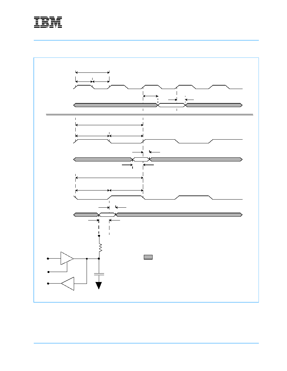
IBM PowerNP NP4GS3
Preliminary
Network Processor
np3_ds_sec02_phys.fm.11
January 29, 2003
Physical Description
Page 63 of 605
Figure 2-8. TBI Timing Diagram
30 pF
TS
+V
DD
/2
50 W
t
XCK
t
XCH
t
XCL
t
RCK
t
RCH
t
RCL
t
RCL
t
RCH
Tx_Clk
Tx_Data
Rx_Clk0
Rx_Clk1
Rx_Data
Transmit Timings
Receive Timings
t
DD
(MAX)
t
DD
(MIN)
t
RDH
t
RDS
t
RDH
t
RDS
t
RSH
t
RSS
Rx_Data
t
RCK
Notes:
1) V
DD
= 3.3 V
2)
Data Invalid
3) Output Load 50 ohms and 30 pf

IBM PowerNP NP4GS3
Network Processor
Preliminary
Physical Description
Page 64 of 605
np3_ds_sec02_phys.fm.11
January 29, 2003
Table 2-20. TBI Timing Diagram Legend (for Figure 2-8)
Symbol
Symbol Description
Minimum (ns)
Maximum (ns)
t
XCK
Tx_Clk Transmit Cycle Time
8
t
XCH
Tx_Clk Pulse Width High
3.5
4.0
t
XCL
Tx_Clk Pulse Width Low
4.0
4.5
t
DD
Tx_Data_(7:0) Output Delay
3.2
4.7
t
RCK
Rx_Clk0/Rx_Clk1 Receive Cycle Time
16
t
RCH
Rx_Clk0/Rx_Clk1 Pulse Width High
7
t
RCL
Rx_Clk0/Rx_Clk1 Pulse Width Low
7
t
RDS
Rx_Data_(9:0) Setup Time Clk0
0.7
t
RDH
Rx_Data_(9:0) Hold Time Clk0
1.2
t
RDS
Rx_Data_(9:0) Setup Time Clk1
0.7
t
RDH
Rx_Data_(9:0) Hold Time Clk1
1.2
Note: All delays are measured with 1 ns slew time measured from 10-90% of input voltage.

IBM PowerNP NP4GS3
Preliminary
Network Processor
np3_ds_sec02_phys.fm.11
January 29, 2003
Physical Description
Page 65 of 605
2.1.5.2 GMII Bus Pins
Table 2-21. PMM Interface Pins: GMII Mode
Signal
Description
Type
Tx_Data(7:0)
Transmit Data. Data bus to the PHY, synchronous to Tx_Clk.
Output
5.0 V-tolerant
3.3 V LVTTL
Rx_Data(7:0)
Received Data. Data bus from the PHY, synchronous to Rx_Clk.
Input
5.0 V-tolerant
3.3 V LVTTL
Tx_En
Transmit data Enabled to the PHY, synchronous to Tx_Clk.
0
End of frame transmission
1
Active frame transmission
Output
5.0 V-tolerant
3.3 V LVTTL
Tx_Er
Transmit Error, synchronous to the Tx_Clk.
0
No error detected
1
Informs the PHY that MAC detected an error
Output
5.0 V-tolerant
3.3 V LVTTL
Rx_Valid_Byte
Receive valid data, synchronous to the Rx_Clk.
0
Data invalid
1
Byte of data (from the PHY) on Rx_Data is valid.
For a standard GMII connection, this signal can be tied to `1' on the card.
Input
5.0 V-tolerant
3.3 V LVTTL
Tx_Byte_Credit
Transmit next data value, asynchronous.
0
Do not send next data byte
1
Asserted. PHY indicates that the next Tx_Data value may be sent.
For a standard GMII connection, this signal can be tied to `1' on the card.
Input
5.0 V-tolerant
3.3 V LVTTL
Tx_Valid_Byte
Transmit valid data, synchronous to Tx_Clock
0
Data invalid
1
Byte of data (from the Network Processor) on Tx_Data is valid.
Output
5.0 V-tolerant
3.3 V LVTTL
Rx_Clk
125 MHz Receive Medium clock generated by the PHY.
Input
5.0 V-tolerant
3.3 V LVTTL
Rx_DV
Receive Data Valid (from the PHY), synchronous to Rx_Clk.
0
End of frame transmission.
1
Active frame transmission.
Input
5.0 V-tolerant
3.3 V LVTTL
Rx_Er
Receive Error, synchronous to Rx_Clk.
0
No error detected
1
Informs the MAC that PHY detected an error
Input
5.0 V-tolerant
3.3 V LVTTL
Tx_Clk
125 MHz transmit clock to the PHY. During operation, the network processor drives this sig-
nal to indicate that a transmit is in progress for this interface.
Output
5.0 V-tolerant
3.3 V LVTTL
CPDetect
This pin must be pulled low to indicate when a Control Point is active on this DMU interface.
Otherwise, this signal should be pulled high (inactive).
The state of the signal is captured in the Data Mover Unit (DMU) Configuration (page 531)
when the Blade_Reset signal is deasserted.
Input
5.0 V-tolerant
3.3 V LVTTL
Note: The NP4GS3 supports GMII in Full-Duplex Mode only.
See Table 2-16: PMM Interface Pin Multiplexing on page 59 for pin directions (I/O) and definitions.

IBM PowerNP NP4GS3
Network Processor
Preliminary
Physical Description
Page 66 of 605
np3_ds_sec02_phys.fm.11
January 29, 2003
Figure 2-9. GMII Timing Diagram
30 pF
TS
50
t
CK
t
XCH
t
XCL
t
DD
(MIN)
t
DD
(MAX)
t
DEN
(MIN)
t
DEN
(MAX)
t
DER
(MIN)
t
DER
(MAX)
t
DBV
(MIN)
t
DVB
(MAX)
t
RCH
t
RCL
t
RDH
t
RDS
t
RVH
t
RVS
t
REH
t
RES
t
RDVH
t
RDVS
Tx_Clk
Tx_Data
Tx_En
Tx_Er
Tx_Valid_Byte
Rx_Clk
Rx_Data
Rx_Valid_Byte
Rx_Er
Rx_DV
Transmit Timings
Receive Timings
Notes:
1) V
DD
= 3.3 V
2)
Data Invalid
3) Output Load 50 ohms and 30 pf

IBM PowerNP NP4GS3
Preliminary
Network Processor
np3_ds_sec02_phys.fm.11
January 29, 2003
Physical Description
Page 67 of 605
2.1.5.3 SMII Bus Pins
Table 2-22. GMII Timing Diagram Legend (for Figure 2-9)
Symbol
Symbol Description
Minimum (ns)
Maximum (ns)
t
CK
Tx_Clk Cycle Time
8
t
XCH
Transmit Clock Pulse Width High
3.5
3.9
t
XCL
Transmit Clock Pulse Width Low
4.1
4.5
t
RCH
Receive Clock Pulse Width High
2.5
t
RCL
Receive Clock Pulse Width Low
2.5
t
DD
Tx_data Output Delay
3.7
4.6
t
DER
Tx_Er Output Delay
3.7
4.6
t
DVB
Tx_Valid_Byte Output Delay
3.7
4.5
t
DEN
Tx_En Output Delay
3.2
4.7
t
RDS
Rx_data Setup Time
1.9
t
RDH
Rx_data Hold Time
0
t
RVS
Rx_Valid_Byte Setup Time
1.9
t
RVH
Rx_Valid_Byte Hold Time
0
t
RES
Rx_Er Setup Time
1.8
t
REH
Rx_Er Hold Time
0
t
RDVS
Rx_DV Setup Time
1.9
t
RDVH
Rx_DV Hold Time
0
1. All delays are measured with 1 ns slew time measured from 10-90% of input voltage.
Table 2-23. PMM Interface Pins: SMII Mode
Signal
Description
Type
Tx_Data(9:0)
Transmit Data. Data bus to the PHY - contains ten streams of serial transmit data. Each
serial stream is connected to a unique port. Synchronous to the common clock (Clk).
Output
5.0 V-tolerant
3.3 V LVTTL
Rx_Data(9:0)
Received Data. Data bus from the PHY - contains ten streams of serial receive data. Each
serial stream is connected to a unique port. Synchronous to the common clock (Clk).
Input
5.0 V-tolerant
3.3 V LVTTL
Sync
Asserted for one Tx_Clk cycle once every ten Tx_Clk cycles. Assertion indicates the begin-
ning of a 10-bit segment on both Tx_Data and Rx_Data.
Output
5.0 V-tolerant
3.3 V LVTTL
Sync2
Logically identical to Sync and provided for fanout purposes.
Output
5.0 V-tolerant
3.3 V LVTTL
CPDetect
This pin must be pulled low to indicate when a Control Point is active on this DMU inter-
face. Otherwise, this signal should be pulled high (inactive).
The state of the signal is captured in the Data Mover Unit (DMU) Configuration (see 13.25
Data Mover Unit (DMU) Configuration Registers on page 531) when the Blade_Reset sig-
nal is deasserted.
Input
5.0 V-tolerant
3.3 V LVTTL

IBM PowerNP NP4GS3
Network Processor
Preliminary
Physical Description
Page 68 of 605
np3_ds_sec02_phys.fm.11
January 29, 2003
Figure 2-10. SMII Timing Diagram
Table 2-24. SMII Timing Diagram Legend (for Figure 2-10)
Symbol
Symbol Description
Minimum (ns)
Maximum (ns)
t
CK
Clk Cycle Time
8
t
CH
Clk Pulse Width High
4
t
CL
Clk Pulse Width Low
4
t
DD
Tx_data_(9:0) Output Delay
1.9
4.7
tDS
Sync Output Delay
2.2
4.5
tDS2
Sync2 Output Delay
2.3
4.5
tRS
Rx_data_(9:0) Setup Time
0.8
tRH
Rx_data_(9:0) Hold Time
0.2
1. All delays are measured with 1 ns slew time measured from 10-90% of input voltage.
30 pF
TS
+V
DD
/2
50
t
CK
t
CH
t
CL
t
DD
(MIN)
t
DD
(MAX)
t
DS
(MIN)
t
DS
(MAX)
t
DS2
(MIN)
t
DS2
(MAX)
t
RH
t
RS
Clk
Tx_Data
Sync
Sync2
Rx_Data
Transmit Timings
Receive Timings
Notes:
1) V
DD
= 3.3 V
2)
Data Invalid
3) Output Load 50 ohms and 30 pf

IBM PowerNP NP4GS3
Preliminary
Network Processor
np3_ds_sec02_phys.fm.11
January 29, 2003
Physical Description
Page 69 of 605
2.1.5.4 POS Bus Pins
Table 2-25. PMM Interface Pins POS32 Mode
Pin(s)
DMU_A
DMU_B
DMU_C
DMU_D
28
TxPADL(1)
O
27
TxPADL(0)
O
26
TxSOF
O
25
TxEOF
O
(24:17)
TxData(31:24)
O
TxData(23:16)
O
TxData(15:8)
O
TxData(7:0)
O
(16:9)
RxData(31:24)
I
RxData(23:16)
I
RxData(15:8)
I
RxData(7:0)
I
8
--
7
TxEn
O
6
TxPFA
I
5
RxPFA
I
4
RxVal
I
3
Clk
I
10 ns
Clk
I
10 ns
Clk
I
10 ns
Clk
I
10 ns
2
RxEOF
I
1
RxErr
I
0
RxEnb
O
Single Pins (not associated with a DMU)
Pin
Rx_LByte(1:0)
1
Rx_LByte(1)
I
0
Rx_LByte(0)
I

IBM PowerNP NP4GS3
Network Processor
Preliminary
Physical Description
Page 70 of 605
np3_ds_sec02_phys.fm.11
January 29, 2003
Table 2-26. POS Signals
Signal
Description
Type
RxAddr(1:0)
Receive address bus selects a particular port in the framer for a data transfer. Valid on the
rising edge of Clk.
5.0 V-tolerant
3.3 V LVTTL
RxData
(7:0) 8-bit mode
(31:0) 32-bit mode
Receive POS data bus carries the frame word that is read from the Framer's FIFO. RxData
transports the frame data in an 8-bit format.
RxData[7:0] and [31:0] are updated on the rising edge of Clk.
5.0 V-tolerant
3.3 V LVTTL
Clk
POS clock provides timing for the POS Framer interface. Clk must cycle at a 100 MHz or
lower instantaneous rate.
5.0 V-tolerant
3.3 V LVTTL
RxEnb
Receive read enable controls read access from the Framer's receive interface. The
framer's addressed FIFO is selected on the falling edge of RxEnb. Generated on the rising
edge of Clk.
5.0 V-tolerant
3.3 V LVTTL
RxEOF
Receive end-of-frame marks the last word of a frame in RxData. Updated on the rising
edge of Clk.
5.0 V-tolerant
3.3 V LVTTL
RxErr
Receive packet error indicates that the received packet contains an error and must be dis-
carded. Only asserted on the last word of a packet (when RxEOF is also asserted).
Updated on the rising edge of Clk.
5.0 V-tolerant
3.3 V LVTTL
RxVal
Receive valid data output indicates the receive signals RxData, RxEOF, RxErr, and
Rx_LByte are valid from the framer. Updated on the rising edge of Clk.
5.0 V-tolerant
3.3 V LVTTL
Rx_LByte(1:0)
Receive padding length indicates the number of padding bytes included in the last word of
the packet transferred in RxData. Only used when the network processor is configured in
32-bit POS mode. Updated on the rising edge of Clk.
Rx_LByte(1:0) (32-bit mode)
00
packet ends on RxData(7:0) (RxData = DDDD)
01
packet ends on RxData(15:8) (RxData = DDDP)
10
packet ends on RxData(23:16) (RxData = DDPP)
11
packet ends on RxData(31:24) (RxData = DPPP)
5.0 V-tolerant
3.3 V LVTTL
RxPFA
Receive polled frame-available input indicates that the framers polled receive FIFO con-
tains data. Updated on the rising edge of Clk.
5.0 V-tolerant
3.3 V LVTTL
TxData
(7:0) 8-bit mode
(31:0) 32-bit mode
Transmit UTOPIA data bus carries the frame word that is written to the framer's transmit
FIFO. Considered valid and written to a framer's transmit FIFO only when the transmit
interface is selected by using TxEnb. Sampled on the rising edge of Clk.
5.0 V-tolerant
3.3 V LVTTL
TxEn
Transmit write enable controls write access to the transmit interface. A framer port is
selected on the falling edge of TxEnb. Sampled on the rising edge of Clk.
5.0 V-tolerant
3.3 V LVTTL
TxAddr(1:0)
Transmit address bus uses TxEnb to select a particular FIFO within the framer for a data
transfer. Sampled on the rising edge of Clk.
5.0 V-tolerant
3.3 V LVTTL
TxSOF
Transmit start-of-frame marks the first word of a frame in TxData. Sampled on the rising
edge of Clk.
5.0 V-tolerant
3.3 V LVTTL
TxEOF
Transmit end-of-frame marks the last word of a frame in TxData. Sampled on the rising
edge of Clk.
5.0 V-tolerant
3.3 V LVTTL
TxPADL (1:0)
Transmit padding length indicates the number of padding bytes included in the last word of
the packet transferred in TxData. Sampled on the rising edge of Clk.
When configured in 32-bit mode the last word may contain zero, one, two or three padding
bytes and only TxPADL[1:0] is used.
TxPADL[1:0] (32-bit mode)
00
packet ends on TxData[7:0] (TxData = DDDD)
01
packet ends on TxData[15:8] (TxData = DDDP)
10
packet ends on TxData[23:16] (TxData = DDPP)
11
packet ends on TxData[31:24] (TxData = DPPP)
5.0 V-tolerant
3.3 V LVTTL
TxPFA
Transmit polled frame-available output indicates that the polled framer's transmit FIFO has
free available space and the NP4GS3 can write data into the framer's FIFO. Updated on
the rising edge of Clk.
5.0 V-tolerant
3.3 V LVTTL

IBM PowerNP NP4GS3
Preliminary
Network Processor
np3_ds_sec02_phys.fm.11
January 29, 2003
Physical Description
Page 71 of 605
Figure 2-11. POS Transmit Timing Diagram
30 pF
TS
+V
DD
/2
50
t
CK
t
CH
t
CL
t
DD
(MIN)
t
DD
(MAX)
t
DXA
(MIN)
t
DXA
(MAX)
t
DRA
(MIN)
t
DRA
(MAX)
t
DSOF
(MIN)
t
DSOF
(MAX)
Clk
TxData
TxAddr
RxAddr
TxSOF
t
DEOF
(MIN)
t
DEOF
(MAX)
t
DEN
(MIN)
t
DEN
(MAX)
t
DPADL
(MIN)
t
DPADL
(MAX)
t
DREN
(MIN)
t
DREN
(MAX)
TxEOF
TxEN
TxPADL
RxEnb
Notes:
1) V
DD
= 3.3 V
2)
Data Invalid
3) Output Load 50 ohms and 30 pf

IBM PowerNP NP4GS3
Network Processor
Preliminary
Physical Description
Page 72 of 605
np3_ds_sec02_phys.fm.11
January 29, 2003
Figure 2-12. POS Receive Timing Diagram
30 pF
TS
+V
DD
/2
50
Notes:
1) V
DD
= 3.3 V
2)
Data Invalid
3) Output Load 50 ohms and 30 pf
t
CK
t
CH
t
CL
t
RXH
t
RXS
t
RPFH
t
RPFS
t
TPFH
t
TPFS
t
RVH
t
RVS
t
REOFH
t
REOFS
Clk
RxData
RxPFA
RxErr
RxVal
RxEOF
t
TPFH
t
TPFS
TxPFA
t
RPADH
RxPADL
t
RPADS

IBM PowerNP NP4GS3
Preliminary
Network Processor
np3_ds_sec02_phys.fm.11
January 29, 2003
Physical Description
Page 73 of 605
Table 2-27. POS Timing Diagram Legend (for Figure 2-11 and Figure 2-12)
Symbol
Symbol Description
Minimum (ns)
Maximum (ns)
t
CK
Clk Cycle Time
10
t
CH
Clk Clock Width High
2.1
t
CL
Clk Clock Width Low
2.1
t
DD
Tx_data_(31:0) Output Delay
2.2
4.6
t
DXA
Tx_ADDR_(1:0) Output Delay
2.2
4.6
t
DRA
Rx_ADDR_(1:0) Output Delay
2.1
4.3
t
DSOF
TxSOF Output Delay
2.3
4.6
t
DEOF
TxEOF Output Delay
2.2
4.5
t
DEN
TxEn Output Delay
1.9
4.7
t
DPADL
TxPADL_(1:0) Output Delay
2.2
4.6
t
DREN
RxEnb Output Delay
1.5
4.3
t
RXS
Rx_data_(31:0) Setup Time
1.9
t
RXH
Rx_data_(31:0) Hold Time
0
t
RVS
RxVal Setup Time
1.9
t
RVH
RxVal Hold Time
0
t
RERS
RxErr Setup Time
1.8
t
RERH
RxErr Hold Time
0
t
REOFS
RxEOF Setup Time
1.9
t
REOFH
RxEOF Hold Time
0
t
RPFS
RxPFA Setup Time
1.9
t
RPFH
RxPFA Hold Time
0
t
TPFS
TxPFA Setup Time
1.6
t
TPFH
TxPFA Hold Time
0
t
RPADS
RxPADL Setup Time
1.8
t
RPADH
RxPADL Hold Time
0
1. All delays are measured with 1 ns slew time measured from 10-90% of input voltage.

IBM PowerNP NP4GS3
Network Processor
Preliminary
Physical Description
Page 74 of 605
np3_ds_sec02_phys.fm.11
January 29, 2003
2.1.6 PCI Pins
These pins interface with the PCI bus.
Table 2-28. PCI Pins
(Page 1 of 2)
Signal
Description
Type
PCI_Clk
PCI Clock Signal (See PCI_Speed field below)
Input
PCI (in)/
3.3 V
PCI_AD(31:0)
PCI Multiplexed Address and Data Signals
Input/Output
PCI (t/s)
3.3 V
PCI_CBE(3:0)
PCI Command/Byte Enable Signals
Input/Output
PCI (t/s)
3.3 V
PCI_Frame
PCI Frame Signal
Input/Output
PCI (s/t/s)
3.3 V
PCI_IRdy
PCI Initiator (Master) Ready Signal
Input/Output
PCI (s/t/s)
3.3 V
PCI_TRdy
PCI Target (Slave) Ready Signal
Input/Output
PCI (s/t/s)
3.3 V
PCI_DevSel
PCI Device Select Signal
Input/Output
PCI (s/t/s)
3.3 V
PCI_Stop
PCI Stop Signal
Input/Output
PCI (s/t/s)
3.3 V
PCI_Request
PCI Bus Request Signal
Output
PCI (t/s)
3.3 V
PCI_Grant
PCI Bus Grant Signal
Input
PCI (t/s)
3.3 V
PCI_IDSel
PCI Initialization Device Select Signal
Input
PCI (in)
3.3 V
PCI_PErr
PCI Parity Error Signal
Input/Output
PCI (s/t/s)
3.3 V
PCI_SErr
PCI System Error Signal
Input/Output
PCI (o/d)
3.3 V
PCI_IntA
PCI Level Sensitive Interrupt
Output
PCI (o/d)
3.3 V
PCI_Par
PCI Parity Signal. Covers all the data/address and the four command/BE signals.
Input/Output
PCI (t/s)
3.3 V
Note: PCI I/Os are all configured for multi-point operation.

IBM PowerNP NP4GS3
Preliminary
Network Processor
np3_ds_sec02_phys.fm.11
January 29, 2003
Physical Description
Page 75 of 605
PCI_Speed
PCI Speed. Controls Acceptable PCI Frequency Asynchronous Range by setting the PLB/
PCI clock ratio.
0
PLB:PCI Mode 2:1. Acceptable PCI Frequency Asynchronous Range is 34.5 MHz
to 66.6 MHz
1
PLB:PCI Mode 3:1. Acceptable PCI Frequency Asynchronous Range is 23.5 MHz
to 44.5 MHz
Input
3.3 V-tolerant
2.5 V
PCI_Bus_NM_Int
External Non-maskable Interrupt - the active polarity of the interrupt is programmable by the
PowerPC.
Input
PCI
3.3 V
PCI_Bus_M_Int
External Maskable Interrupt - the active polarity of the interrupt is programmable by the
PowerPC.
Input
PCI
3.3 V
Table 2-28. PCI Pins
(Page 2 of 2)
Signal
Description
Type
Note: PCI I/Os are all configured for multi-point operation.

IBM PowerNP NP4GS3
Network Processor
Preliminary
Physical Description
Page 76 of 605
np3_ds_sec02_phys.fm.11
January 29, 2003
Figure 2-13. PCI Timing Diagram
30 pF
TS
50
V
DD
/2
t
CK
t
CH
t
CL
t
VAL
t
ON
t
OFF
Outputs
PCI_Clk
t
DH
t
DS
Inputs
Notes:
1) V
DD
= 3.3 V
2)
Data Invalid
3) Output Load 50 ohms and 30 pf

IBM PowerNP NP4GS3
Preliminary
Network Processor
np3_ds_sec02_phys.fm.11
January 29, 2003
Physical Description
Page 77 of 605
2.1.7 Management Bus Interface Pins
The signals from these pins are translated into various "host" buses by an external field-programmable gate
array (FPGA) Serial/Parallel Manager (SPM).
Table 2-29. PCI Timing Diagram Legend (for Figure 2-13)
Symbol
Symbol Description
Minimum (ns)
Maximum (ns)
t
CK
PCI Cycle Time
15
t
CH
Clk Clock Width High
7.5
t
CL
Clk Clock Width Low
7.5
t
VAL
Worst Case Output Delay
2.0
4.8
t
ON
PCI Bus Turn on Output Delay
2
t
OFF
PCI Bus Turn off Output Delay
14
t
DS
Input Setup Time
2.4
t
DH
Input Hold Time
0
Note: All delays are measured with 1 ns slew time measured from 10-90% of input voltage.
Table 2-30. Management Bus Pins
Signal
Description
Type
MG_Data
Serial Data. Supports Address/Control/Data protocol.
Input/Output
3.3 V-tolerant
2.5 V
MG_Clk
33.33 MHz clock
Output
3.3 V-tolerant
2.5 V
MG_nIntr
Rising-edge sensitive interrupt input
Input
3.3 V-tolerant
2.5 V

IBM PowerNP NP4GS3
Network Processor
Preliminary
Physical Description
Page 78 of 605
np3_ds_sec02_phys.fm.11
January 29, 2003
Figure 2-14. SPM Bus Timing Diagram
Table 2-31. SPM Bus Timing Diagram Legend (for Figure 2-14)
Symbol
Symbol Description
Minimum (ns)
Maximum (ns)
t
CK
SPM Cycle Time
30
t
CH
Clock Pulse Width High
14.4
15.6
t
CL
Clock Pulse Width Low
14.4
15.6
t
DD
Data Output Delay
6.9
7.9
t
DS
Data Setup Time
5.1
t
DH
Data Hold Time
0
Note: mg_nintr is an asynchronous input and is not timed.
All delays are measured with 1 ns slew time measured from 10-90% of input voltage.
30 pF
TS
50
V
DD
/2
t
CK
t
CH
t
CL
t
DD
(MAX)
Outputs
MG_Clk
t
DH
t
DS
Inputs
t
DD
(MIN)
MG_Data
MG_Data
Notes:
1) V
DD
= 3.3 V
2)
Data Invalid
3) Output Load 50 ohms and 30 pf

IBM PowerNP NP4GS3
Preliminary
Network Processor
np3_ds_sec02_phys.fm.11
January 29, 2003
Physical Description
Page 79 of 605
2.1.8 Miscellaneous Pins
Table 2-32. Miscellaneous Pins
(Page 1 of 2)
Signal
Description
Type
Switch_Clock_A
The positive pin of an input differential pair. 50.6875 to 62.5 MHz. Generates Packet Routing
Switch clock domains. Required to have cycle-to-cycle jitter
�150 ps. Duty Cycle tolerance
must be
�10%. An on-chip differential terminator of 100 ohms is present between this pin
and its complement pin.
Input
LVDS (see
page 581)
Switch_Clock_A
The negative pin of an input differential pair. 50.6875 to 62.5 MHz.
Input
LVDS (see
page 581)
Switch_Clock_B
The positive pin of an input differential pair. 50.6875 to 62.5 MHz. Generates Packet Routing
Switch clock domains. Required to have cycle-to-cycle jitter
�150 ps. Duty Cycle tolerance
must be
�10%. An on-chip differential terminator of 100 ohms is present between this pin
and its complement pin.
Input
LVDS (see
page 581)
Switch_Clock_B
The negative pin of an input differential pair. 50.6875 to 62.5 MHz.
Input
LVDS (see
page 581)
Switch_BNA
Selects which of the two DASL ports (A or B) carries network traffic.
0
Port A carries the network traffic
1
Port B carries the network traffic
Input
5.0 V-tolerant
3.3 V LVTTL
Core_Clock
53.33 MHz oscillator - generates 266 /133 clock domains. Required to have cycle-to-cycle
jitter
�150 ps. Duty Cycle tolerance must be �10%.
Input
5.0 V-tolerant
3.3 V LVTTL
Clock125
125 MHz oscillator. Required to have cycle-to-cycle jitter
�60 ps. Duty Cycle tolerance
must be
� 5%. This clock is required only when supporting TBI and GMII DMU bus modes.
Input
5.0 V-tolerant
3.3 V LVTTL
Blade_Reset
Reset NP4GS3 - signal must be driven active low for a minimum of 1
�s to ensure a proper
reset of the NP4GS3. All input clocks (Switch_Clock_A, Switch_Clock_A, Switch_Clock_B,
Switch_Clock_B, Core_Clock, Clock125 if in use, and PCI_Clk) must be running prior to the
activation of this signal.
Input
5.0 V-tolerant
3.3 V LVTTL
Operational
NP4GS3 operational - pin is driven active low when both the NP4GS3 Ingress and Egress
Macros have completed their initialization. It remains active until a subsequent Blade_Reset
is issued.
Output (o/d)
5.0 V-tolerant
3.3 V LVTTL
Testmode(1:0)
00
Functional Mode, including concurrent use of the JTAG interface for RISCWatch or
CABWatch operations.
01
Debug Mode - Debug mode must be indicated by the Testmode I/O for debug bus
(DMU_D) output to be gated from the probe.
10
JTAG Test Mode
11
LSSD Test Mode
Input
CMOS
1.8 V
JTAG_TRst
JTAG test reset. For normal functional operation, this pin must be connected to the same
card source that is connected to the Blade_Reset input. When the JTAG interface is used for
JTAG test functions, this pin is controlled by the JTAG interface logic on the card.
Input
5.0 V-tolerant
3.3 V LVTTL
JTAG_TMS
JTAG test mode select. For normal functional operation, this pin should be tied either low or
high.
Input
5.0 V-tolerant
3.3 V LVTTL
JTAG_TDO
JTAG test data out. For normal functional operation, this pin should be tied either low or
high.
Output
5.0 V-tolerant
3.3 V LVTTL
JTAG_TDI
JTAG test data in. For normal functional operation, this pin should be tied either low or high.
Input
5.0 V-tolerant
3.3 V LVTTL

IBM PowerNP NP4GS3
Network Processor
Preliminary
Physical Description
Page 80 of 605
np3_ds_sec02_phys.fm.11
January 29, 2003
The termination network details for the signals are contained in the IBM PowerNP NP4GS3 PC Card Layout
Guidelines.
JTAG_TCk
JTAG test clock. For normal functional operation, this pin should be tied either low or high.
Input
5.0 V-tolerant
3.3 V LVTTL
PLLA_V
DD
PLLB_V
DD
PLLC_V
DD
These pins serve as the +1.8 Volt supply for a critical noise-sensitive portion of the phase-
locked loop (PLL) circuits. One pin serves as the analog V
DD
for each PLL circuit. To prevent
noise on these pins from introducing phase jitter in the PLL outputs, place filters at the board
level to isolate these pins from the noisy digital V
DD
pins. Place separate filters on each ana-
log V
DD
pin to prevent noise from one PLL being introduced into another.
See section 2.1.9 PLL Filter Circuit on page 82 for filter circuit details.
Input
PLL_V
DD
1.8 V
PLLA_GND
PLLB_GND
PLLC_GND
These pins serve as the ground connection for the critical noise portion of the phase lock
loop (PLL). One pin serves as the analog GND for each PLL circuit. Each should be con-
nected to the digital ground plane at the V
DDA
node of the PLL filter capacitor shown in Fig-
ure 2-15: PLL Filter Circuit Diagram on page 82.
Input
PLL_GND
0.0 V
Thermal_In
Input pad of the thermal monitor (resistor). See 2.1.10 Thermal I/O Usage on page 82 for
details on thermal monitor usage
Thermal
Thermal_Out
Output pad of the thermal monitor (resistor)
Thermal
VRef1(2), VRef2(8,7,6)
Voltage reference for SSTL2 I/Os for D1, D2, and D3 (approximately four pins per side of the
device that contains SSTL2 I/O)
Input
VRef
1.25 V
VRef1(1), VRef2(5,4,3)
Voltage reference for SSTL2 I/Os for D4 and D6 (approximately four pins per side of the
device that contains SSTL2 I/O)
Input
VRef
1.25 V
VRef1(0), VRef2(2,1,0)
Voltage reference for SSTL2 I/Os for DS0 and DS1 (approximately four pins per side of the
device that contains SSTL2 I/O)
Input
VRef
1.25 V
Boot_Picocode
Determines location of network processor picocode load location.
0
Load from SPM
1
Load from external source (typically Power PC or PCI bus)
Input
3.3 V-tolerant
2.5 V
Boot_PPC
Determines location of Power PC code start location.
0
Start from D6
1
Start from PCI
Input
3.3 V-tolerant
2.5 V
Spare_Tst_Rcvr(9:0)
Unused signals needed for Manufacturing Test.
Spare_Tst_Rcvr (9:5,1) should be tied to 0 on the card.
Spare_Tst_Rcvr (4:2,0) should be tied to 1 on the card.
Input
CMOS
1.8 V
C405_Debug_Halt
This signal, when asserted low, forces the embedded PowerPC 405 processor to stop pro-
cessing all instructions. For normal functional operation, this signal should be tied inactive
high.
Input
5.0 V-tolerant
3.3 V LVTTL
PIO(2:0)
Programmable I/O
Input/Output
CMOS
2.5V
PGM_GND
PGM_VDD
These IO are used for chip manufacturing and test purposes and should be left unconnected
on the card.
-
Table 2-32. Miscellaneous Pins
(Page 2 of 2)
Signal
Description
Type

IBM PowerNP NP4GS3
Preliminary
Network Processor
np3_ds_sec02_phys.fm.11
January 29, 2003
Physical Description
Page 81 of 605
Table 2-33. Signals Requiring Pull-Up or Pull-Down
Signal Name
Function
Value
Signals requiring a DC connection that is the same value for all applications
Testmode(1:0)
Pull-down
JTAG_TDI
Pull-up
JTAG_TMS
Pull-up
JTAG_TCk
Pull-up
C405_Debug_Halt
Pull-up
Spare_Tst_Rcvr (9:5, 1)
Pull-down
Spare_Tst_Rcvr (4:2, 0)
Pull-up
Signals requiring a DC connection that varies across different applications
Multicast_Grant_A, Multicast_Grant_B
Pull-up if no system device drives this signal
RES_Data, RES_sync
Pull-down if no other system device drives this signal
PCI_Speed
Choose up or down based on system PCI bus speed
MG_nIntr
Pull-down if no system device drives this signal
MG_Data
Pull-down when external SPM module is attached
Boot_Picocode
Choose up or down based on picocode load location
Boot_PPC
Choose up or down based on PPC code load location
Switch_BNA
Pull-up if no system device drives this signal
LU_R_WRT, SCH_R_WRT
Pull up when system diagnostics uses ZBT SRAM to
hold information through a software controlled reset
(see Software Controlled Reset Register (Soft_Reset)
on page 485).
Rx_LByte(1:0)
Pull down if not using 32-bit POS mode.
Signals which have an AC connection, but also require pull-up or pull-down
Operational
Pull-up
DMU_A(0), DMU_B(0), DMU_C(0), DMU_D(0)
CPDetect
If control point blade then pull-down, otherwise pull-up
DMU_A(30:29), DMU_B(30:29),
DMU_C(30:29), DMU_D(30:29)
DMU in 8-bit POS
mode. RxAddr (1:0)
Pull-down
DMU_A(4), DMU_B(4), DMU_C(4), DMU_D(4)
DMU in any POS
mode. RxVal
Pull-down
D3_DQS(1:0), D2_DQS(1:0), D1_DQS(1:0)
Pull-down
D0_DQS(3:0), D4_DQS(3:0), D6_DQS(3:0)
Pull-down
DS0_DQS(3:0), DS1_DQS(3:0)
Pull-down
Note: In addition to the signals listed in this table, any interface signals that are not used for a particular application should be pulled to
their inactive state (for control signals) or down to ground (for data signals). This prevents extraneous switching of the circuitry, which
can cause current surges that could affect other signals. Pull-down resistors should be in the range of 300�1000
. If the signals are not
being actively driven, up to eight signals can be connected to a single pull-down. If this is done, the resistance value of that pull-down
should be kept close to the low end of the range.

IBM PowerNP NP4GS3
Network Processor
Preliminary
Physical Description
Page 82 of 605
np3_ds_sec02_phys.fm.11
January 29, 2003
2.1.9 PLL Filter Circuit
V
DDA
is the voltage supply pin to the analog circuits in the PLL. Noise on V
DDA
causes phase jitter at the
output of the PLL. V
DDA
is brought to a package pin to isolate it from the noisy internal digital V
DD
signal. If
little noise is expected at the board level, then V
DDA
can be connected directly to the digital V
DD
plane. In
most circumstances, however, it is prudent to place a filter circuit on the V
DDA
as shown below.
Note: All wire lengths should be kept as short as possible to minimize coupling from other signals.
The impedance of the ferrite bead should be much greater than that of the capacitor at frequencies where
noise is expected. Many applications have found that a resistor does a better job of reducing jitter than a
ferrite bead does. The resistor should be kept to a value lower than 2
. Experimentation is the best way to
determine the optimal filter design for a specific application.
Note: One filter circuit may be used for PLLA and PLLB, and a second filter circuit should be used for PLLC.
2.1.10 Thermal I/O Usage
The thermal monitor consists of a resistor connected between pins PADA and PADB. At 2
5�C this resistance
is estimated at 1500 + 350 ohms. The published temperature coefficient of the resistance for this technology
is 0.33% per
�C. To determine the actual temperature coefficient, see Measurement Calibration on page 83.
Note: There is an electrostatic discharge (ESD) diode at PADA and PADB.
Figure 2-15. PLL Filter Circuit Diagram
Figure 2-16. Thermal Monitor
GND
Digital VDD
(via at board)
VDDA
(to PLL)
Ferrite Bead
C = 0.1
�F
Thermal
PADA
PADB
IBM PowerNP NP4GS3
Preliminary
Network Processor
np3_ds_sec02_phys.fm.11
January 29, 2003
Physical Description
Page 83 of 605
2.1.10.1 Temperature Calculation
The chip temperature can be calculated from
where:
R
measured
= resistance measured between PADA and PADB at test temperature.
R
calibrated
= resistance measured between PADA and PADB (V r /I dc ) at known temperature.
T
calibrated
= known temperature used to measure R calibrated.
2.1.10.2 Measurement Calibration
To use this thermal monitor accurately, it must first be calibrated. To calibrate, measure the voltage drop at
two different known temperatures at the package while the device is dissipating little
(less than 100 mW) or
no power. Apply I
dc
and wait for a fixed time t
m
, where t
m
= approximately 1 ms. Keep t
m
short to
minimize heating effects on the thermal monitor resistance. Then measure V
r
. Next, turn off I
dc
and
change the package temperature. Reapply I
dc
, wait t
m
again and measure V
r
.
The temperature coefficient is,
,
where:
T = temperature change,
�C
V
r
= voltage drop, V
I
dc
= applied current, A
t
c
(R
measured
- R
calibrated
)
T
chip
=
1
+ T
calibrated
�C
Tc
Vr
Idc
T
�
----------------------
�C
------
=
PADB
PADA
V
r
measure voltage drop
V
supply
= V
DD
Maximum
I
dc
= 200
�A Maximum
Thermal
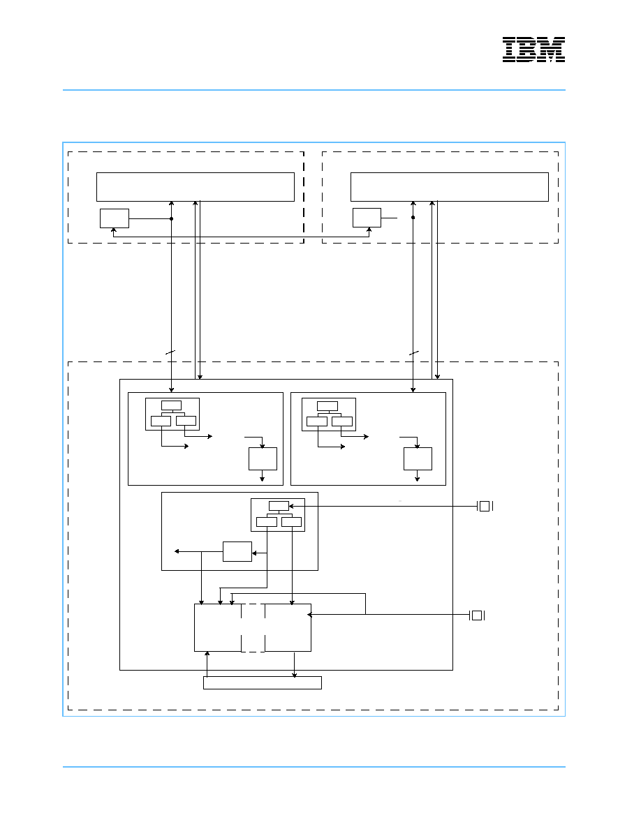
IBM PowerNP NP4GS3
Network Processor
Preliminary
Physical Description
Page 84 of 605
np3_ds_sec02_phys.fm.11
January 29, 2003
2.2 Clocking Domains
See NP4GS3 DMU Bus Clock Connections on page 60 and NP4GS3 DMU Bus Clock Connections (POS
Overview) on page 61 for related clock information.
Figure 2-17. Clock Generation and Distribution
PLL
Packet Routing Switch
4.54-5 ns
Clock Domain
9.09 ns
x8
/4
/4
x16
/8
IBM 28.4G Packet Routing Switch
D
ASL-A
Switch Fabric Card A
Switch Blade
OSC
IBM 28.4G Packet Routing Switch
Switch Fabric Card B
OSC
S
w
it
c
h
_C
l
k
_
A
(
5
5 M
H
z
)
S
w
it
c
h
_C
l
k
_
B
(
5
5 M
H
z
)
D
ASL-B
PLL
Packet Routing Switch
4.54-5 ns
Clock Domain
9.09 ns
x8
53.3 MHz
125 MHz
2
2
Divide
by 2
7.5 ns
IBM NP4GS3
/4
/4
Tx_Clk
Rx_Clk
PHY and POS Devices
3.75 ns
8 ns
Core, DDR, ZBT
Clock_Core
Clock Domain
SMII, TBI, and GMII
x16
/8
PLL
x8
/4
/3
x15
/8
Clock Domain
frequency lock
Divide
by 4
36.3 ns
Divide
by 4
36.3 ns
10 ns
Clock125 - TBI, GMII
DMU_*(03) - SMII
Note: Switch_Clk_A and B frequencies are
shown for illustration purposes. These
clocks can range from 50.6875 to 62.5 MHz.

IBM PowerNP NP4GS3
Preliminary
Network Processor
np3_ds_sec02_phys.fm.11
January 29, 2003
Physical Description
Page 85 of 605
Figure 2-18. Pins Diagram
W V U T R P
N M L
K J
H G F E D C B
A
01
02
03
04
05
06
07
08
09
10
11
12
13
14
15
16
17
18
19
AD AC AB AA Y
20
21
22
23
24
25
Corner
AE
AF
AG
AH
AJ
AK
AL
AM
AN
Signal = 815
Test I/O
Ground = 137
V
DD
= 72
V
DD2
(3.3 V) = 16
1
2
V
DD3
(2.5 V) = 16
V
DD4
(2.5 V) = 16
3
4
V
DD5
(2.5 V) = 16
5
DC Test I/O
1
4
1
4
1
4
1
4
1
4
1
1
3
4
1
4
1
4
5
4
1
4
1
1
5
4
1
1
1
4
3
1
5
1
1
4
4
1
1
3
1
4
1
5
4
3
1
3
1
1
5
1
1
5
1
3
1
3
5
1
5
1
1
1
3
1
1
1
1
2
1
2
1
2
1
2
1
2
1
2
5
1
1
2
1
2
1
1
1
2
1
2
3
1
1
2
5
2
1
1
3
1
5
2
1
1
2
3
1
5
2
5
1
2
1
3
1
1
1
1
5
1
5
1
3
3
1
1
1
1
5
1
3
1
3
1
26
27
28
29
30
31
32
33
Note: For illustrative purposes only.
Viewed through top of package
A01

IBM PowerNP NP4GS3
Network Processor
Preliminary
Physical Description
Page 86 of 605
np3_ds_sec02_phys.fm.11
January 29, 2003
2.3 Mechanical Specifications
Figure 2-19. Mechanical Diagram
Notes:
1. Refer to Table 2-34 on page 87 for mechanical dimensions.
2. Mechanical drawing is not to scale. See your IBM representative for more information.
3. IBM square outline conforms to JEDEC MO-158.
A
A1
DLA
Lidless
DLA
Chip
aaa
D
E
E1
D1
e
�ccc
�ccc
b
Note: No I/O at A01 location
�ddd M
�eee M
Z
Z
X Y
A
A1
aaa
Z
Y
X
Terminal A01 identifier
Top view
Bottom view
Z

IBM PowerNP NP4GS3
Preliminary
Network Processor
np3_ds_sec02_phys.fm.11
January 29, 2003
Physical Description
Page 87 of 605
Table 2-34. Mechanical Specifications
Mechanical Dimensions
Value
1
A (DLA)
Min
2
6.23
Max
3
6.83
A (Lidless)
Min
2
4.23
Max
3
4.83
A1
Nom
2.21
b
Min
0.48
Max
0.52
e
Basic
1.27
aaa
0.15
ccc
0.20
ddd
0.30
eee
0.10
D
42.50
D1
40.64
E
42.50
E1
40.64
M
4
33 x 33
N
5
1088
5
Weight (g)
TBD
1. All dimensions are in millimeters, except where noted.
2. Minimum package thickness is calculated using the nominal thickness of all parts. The nominal thickness of an 8-layer package
was used for the package thickness.
3. Maximum package thickness is calculated using the nominal thickness of all parts. The nominal thickness of a 12-layer package
was used for the package thickness.
4. M = the I/O matrix size.
5. N = the maximum number of I/Os. The number of I/Os shown in the table is the amount after depopulation. Product with 1.27 mm
pitch is depopulated by one I/O at the A01 corner of the array.

IBM PowerNP NP4GS3
Network Processor
Preliminary
Physical Description
Page 88 of 605
np3_ds_sec02_phys.fm.11
January 29, 2003
2.4 IEEE 1149 (JTAG) Compliance
2.4.1 Statement of JTAG Compliance
The NP4GS3 is compliant with IEEE Standard 1149.1a.
2.4.2 JTAG Compliance Mode
Compliance with IEEE 1149.1a is enabled by applying a compliance-enable pattern to the compliance-enable
inputs as shown in Table 2-35.
2.4.3 JTAG Implementation Specifics
All mandatory JTAG public instructions are implemented in the NP4GS3's design. Table 2-36 documents all
implemented public instructions.
Table 2-35. JTAG Compliance-Enable Inputs
Compliance-Enable Inputs
Compliance-Enable Pattern
Testmode(1:0)
`10'
Spare_Tst_Rcvr(9)
1
Spare_Tst_Rcvr(4)
1
Spare_Tst_Rcvr(3)
1
Spare_Tst_Rcvr(2)
1
Note: To achieve reset of the JTAG test logic, the JTAG_TRst input must be driven low when the compliance-enable pattern is applied.
Table 2-36. Implemented JTAG Public Instructions
Instruction Name
Binary Code
1
Serial Data Reg
connected to TDI/TDO
I/O Control Source
(driver data and driver enable)
BYPASS
111 1111
Bypass
System, functional values
CLAMP
111 1101
Bypass
JTAG
EXTEST
111 1000
BoundaryScan
JTAG
HIGHZ
111 1010
Bypass
JTAG, all drivers disabled
SAMPLE/PRELOAD
111 1001
BoundaryScan
System, functional values
1. Device TDO output driver is only enabled during TAP Controller states Shift_IR and Shift_DR.

IBM PowerNP NP4GS3
Preliminary
Network Processor
np3_ds_sec02_phys.fm.11
January 29, 2003
Physical Description
Page 89 of 605
2.4.4 Brief Overview of JTAG Instructions
Instruction
Description
BYPASS
Connects the bypass data register between the TDI and TDO pins. The bypass data register is a single
shift-register stage that provides a minimum-length serial path between the TDI and TDO pins when no
test operation of the device is required. Bypass does not disturb the normal functional connection and
control of the I/O pins.
CLAMP
Causes all output pins to be driven from the corresponding JTAG parallel boundary scan register. The
SAMPLE/PRELOAD instruction is typically used to load the desired values into the parallel boundary
scan register. Since the clamp instruction causes the serial TDI/TDO path to be connected to the
bypass data registers, scanning through the device is very fast when the clamp instruction is loaded.
EXTEST
Allows the JTAG logic to control output pin values by connecting each output data and enable signal to
its corresponding parallel boundary scan register. The desired controlling values for the output data
and enable signals are shifted into the scan boundary scan register during the shiftDR state. The paral-
lel boundary scan register is loaded from the scan boundary scan register during the updateDR state.
The EXTEST instruction also allows the JTAG logic to sample input receiver and output enable values.
The values are loaded into the scan boundary scan register during captureDR state.
HIGHZ
Causes the JTAG logic to tri-state all output drivers while connecting the bypass register in the serial
TDI/TDO path.
SAMPLE/PRELOAD
Allows the JTAG logic to sample input pin values and load the parallel boundary scan register without
disturbing the normal functional connection and control of the I/O pins. The sample phase of the
instruction occurs in captureDR state, at which time the scan boundary scan register is loaded with the
corresponding input receiver and output enable values. (Note that for input pins that are connected to a
common I/O, the scan boundary scan register only updates with a input receiver sample if the corre-
sponding output driver of the common I/O is disabled; otherwise the scan register is updated with the
output data signal.)
The desired controlling values for the output pins are shifted into the scan boundary scan register dur-
ing the shiftDR state and loaded from the scan boundary scan register to the parallel boundary scan
register during the updateDR state.

IBM PowerNP NP4GS3
Preliminary
Network Processor
np3_ds_sec02_phys_pinlist1.fm.11
January 29, 2003
Not Approved For Customer Distribution
Page 90 of 605
Table 2-37. Complete Signal Pin Listing by Signal Name
(Continued)
2.5 Signal Pin Lists
Table 2-37. Complete Signal Pin Listing by Signal Name
Signal Name
Grid
Position
Blade_Reset
E29
Boot_Picocode
K07
Boot_PPC
L04
C405_Debug_Halt
AB23
cam_cp_response(00)
U09
cam_cp_response(01)
T11
cam_cp_response(02)
P05
cam_cp_response(03)
R06
cam_cp_response(04)
T13
cam_cp_response(05)
P07
cam_cp_response(06)
T05
cam_cp_response(07)
R01
cam_cp_response(08)
R10
cam_cp_response(09)
P09
cam_cp_response(10)
R09
cam_cp_response(11)
R14
cam_cp_response(12)
R13
cam_cp_response(13)
N07
Clock125
B33
Core_Clock
C33
D0_Addr(00)
AL10
D0_Addr(01)
AN10
D0_Addr(02)
AJ09
D0_Addr(03)
AN06
D0_Addr(04)
AA14
D0_Addr(05)
AB15
D0_Addr(06)
AM07
D0_Addr(07)
AL08
D0_Addr(08)
AM11
D0_Addr(09)
AL11
D0_Addr(10)
AC14
D0_Addr(11)
AG10
D0_Addr(12)
AF11
D0_CS
AN09
D0_Data(00)
AA12
D0_Data(01)
AD09
D0_Data(02)
AG07
D0_Data(03)
AB11
D0_Data(04)
AN02
D0_Data(05)
AM03
D0_Data(06)
AN01
D0_Data(07)
AN03
D0_Data(08)
AL04
D0_Data(09)
AG03
D0_Data(10)
AH07
D0_Data(11)
AE09
D0_Data(12)
AL03
D0_Data(13)
AC11
D0_Data(14)
AJ06
D0_Data(15)
AK05
D0_Data(16)
AJ07
D0_Data(17)
AN04
D0_Data(18)
AN07
D0_Data(19)
AL07
D0_Data(20)
AF09
D0_Data(21)
AG08
D0_Data(22)
AE10
D0_Data(23)
AD11
D0_Data(24)
AN08
D0_Data(25)
AL09
D0_Data(26)
AL06
D0_Data(27)
AM05
D0_Data(28)
AB13
D0_Data(29)
AC15
D0_Data(30)
AK07
D0_Data(31)
AJ08
D0_DQS(0)
AG09
D0_DQS(1)
AC12
Signal Name
Grid
Position
D0_DQS(2)
AE11
D0_DQS(3)
AH09
D0_WE
AM09
D1_Addr(00)
AB17
D1_Addr(01)
AJ13
D1_Addr(02)
AK13
D1_Addr(03)
AM15
D1_Addr(04)
AN14
D1_Addr(05)
AG12
D1_Addr(06)
AF13
D1_Addr(07)
AE14
D1_Addr(08)
AN15
D1_Addr(09)
AL14
D1_Addr(10)
W16
D1_Addr(11)
AH15
D1_Addr(12)
AJ15
D1_CS
AD15
D1_Data(00)
AE12
D1_Data(01)
AN11
D1_Data(02)
AL12
D1_Data(03)
AJ10
D1_Data(04)
AK09
D1_Data(05)
Y15
D1_Data(06)
AA15
D1_Data(07)
AJ11
D1_Data(08)
AK11
D1_Data(09)
AL13
D1_Data(10)
AN12
D1_Data(11)
AH11
D1_Data(12)
AM13
D1_Data(13)
AN13
D1_Data(14)
AH13
D1_Data(15)
AC16
D1_DQS(0)
AJ14
Signal Name
Grid
Position

IBM PowerNP NP4GS3
Preliminary
Network Processor
np3_ds_sec02_phys_pinlist1.fm.11
January 29, 2003
Page 91 of 605
Table 2-37. Complete Signal Pin Listing by Signal Name
(Continued)
D1_DQS(1)
AN16
D1_WE
AL16
D2_Addr(00)
AJ22
D2_Addr(01)
AH21
D2_Addr(02)
AN21
D2_Addr(03)
AM21
D2_Addr(04)
AH23
D2_Addr(05)
AC20
D2_Addr(06)
AD21
D2_Addr(07)
AG23
D2_Addr(08)
AN22
D2_Addr(09)
AL21
D2_Addr(10)
AK23
D2_Addr(11)
AJ23
D2_Addr(12)
AA19
D2_CS
AL22
D2_Data(00)
AN18
D2_Data(01)
AJ19
D2_Data(02)
W18
D2_Data(03)
AA18
D2_Data(04)
AJ20
D2_Data(05)
AL20
D2_Data(06)
AN19
D2_Data(07)
AE20
D2_Data(08)
AE17
D2_Data(09)
AE21
D2_Data(10)
AG22
D2_Data(11)
AN20
D2_Data(12)
AM19
D2_Data(13)
AK21
D2_Data(14)
AJ21
D2_Data(15)
Y19
D2_DQS(0)
AB19
D2_DQS(1)
AK25
D2_WE
AJ24
Signal Name
Grid
Position
D3_Addr(00)
AG19
D3_Addr(01)
AJ16
D3_Addr(02)
AF17
D3_Addr(03)
AJ17
D3_Addr(04)
AG18
D3_Addr(05)
AE18
D3_Addr(06)
AA17
D3_Addr(07)
AC18
D3_Addr(08)
AK19
D3_Addr(09)
AL19
D3_Addr(10)
AN17
D3_Addr(11)
AK17
D3_Addr(12)
AE19
D3_CS
AL18
D3_Data(00)
AG13
D3_Data(01)
AA16
D3_Data(02)
AG14
D3_Data(03)
AE15
D3_Data(04)
AL17
D3_Data(05)
AM17
D3_Data(06)
AL15
D3_Data(07)
AK15
D3_Data(08)
W17
D3_Data(09)
AE16
D3_Data(10)
AG16
D3_Data(11)
AH17
D3_Data(12)
AG17
D3_Data(13)
AG15
D3_Data(14)
AF15
D3_Data(15)
AF19
D3_DQS(0)
AG20
D3_DQS(1)
AC17
D3_WE
AD19
D4_Addr(00)
C12
D4_Addr(01)
A11
Signal Name
Grid
Position
D4_Addr(02)
J12
D4_Addr(03)
H11
D4_Addr(04)
G10
D4_Addr(05)
L13
D4_Addr(06)
C11
D4_Addr(07)
B11
D4_Addr(08)
D09
D4_Addr(09)
C08
D4_Addr(10)
M13
D4_Addr(11)
N14
D4_Addr(12)
B07
D4_CS
E10
D4_Data(00)
M17
D4_Data(01)
L16
D4_Data(02)
D15
D4_Data(03)
C15
D4_Data(04)
A17
D4_Data(05)
D17
D4_Data(06)
H09
D4_Data(07)
G14
D4_Data(08)
G13
D4_Data(09)
K15
D4_Data(10)
C16
D4_Data(11)
A16
D4_Data(12)
E15
D4_Data(13)
F15
D4_Data(14)
R17
D4_Data(15)
N16
D4_Data(16)
E14
D4_Data(17)
C14
D4_Data(18)
E09
D4_Data(19)
A15
D4_Data(20)
L15
D4_Data(21)
J14
D4_Data(22)
G12
Signal Name
Grid
Position

IBM PowerNP NP4GS3
Network Processor
Preliminary
Page 92 of 605
np3_ds_sec02_phys_pinlist1.fm.11
January 29, 2003
Table 2-37. Complete Signal Pin Listing by Signal Name
(Continued)
D4_Data(23)
H13
D4_Data(24)
A14
D4_Data(25)
B15
D4_Data(26)
D13
D4_Data(27)
E13
D4_Data(28)
P15
D4_Data(29)
E12
D4_Data(30)
F13
D4_Data(31)
A13
D4_DQS(0)
D11
D4_DQS(1)
E11
D4_DQS(2)
N15
D4_DQS(3)
M15
D4_WE
F11
D6_Addr(00)
AL28
D6_Addr(01)
AN26
D6_Addr(02)
AE24
D6_Addr(03)
AG26
D6_Addr(04)
AF25
D6_Addr(05)
AL27
D6_Addr(06)
AN30
D6_Addr(07)
AJ27
D6_Addr(08)
AK29
D6_Addr(09)
AJ28
D6_Addr(10)
AL29
D6_Addr(11)
AG21
D6_Addr(12)
AH27
D6_ByteEn(0)
AG24
D6_ByteEn(1)
AF23
D6_CS
AL31
D6_Data(00)
AL23
D6_Data(01)
AM23
D6_Data(02)
AL26
D6_Data(03)
AM27
D6_Data(04)
AB21
Signal Name
Grid
Position
D6_Data(05)
AN28
D6_Data(06)
AN24
D6_Data(07)
AL24
D6_Data(08)
AH25
D6_Data(09)
AE23
D6_Data(10)
AC21
D6_Data(11)
AN25
D6_Data(12)
AJ26
D6_Data(13)
AK27
D6_Data(14)
AE22
D6_Data(15)
AC22
D6_DQS(0)
AL30
D6_DQS(1)
AN31
D6_DQS(2)
AN33
D6_DQS(3)
AM31
D6_DQS_Par(00)
AN32
D6_DQS_Par(01)
AF21
D6_Parity(00)
AM29
D6_Parity(01)
AN23
D6_WE
AJ25
DA_BA(0)
AN29
DA_BA(1)
AA20
DA_CAS
AN27
DA_Clk
AM25
DA_Clk
AL25
DA_RAS
AG25
DASL_In_A(0)
AK01
DASL_In_A(0)
AJ02
DASL_In_A(1)
AF01
DASL_In_A(1)
AE02
DASL_In_A(2)
AH01
DASL_In_A(2)
AH03
DASL_In_A(3)
AE01
DASL_In_A(3)
AE03
DASL_In_A(4)
AD03
Signal Name
Grid
Position
DASL_In_A(4)
AD01
DASL_In_A(5)
AC02
DASL_In_A(5)
AC03
DASL_In_A(6)
AB03
DASL_In_A(6)
AA04
DASL_In_A(7)
AA03
DASL_In_A(7)
Y03
DASL_In_B(0)
E02
DASL_In_B(0)
D01
DASL_In_B(1)
J02
DASL_In_B(1)
H01
DASL_In_B(2)
F03
DASL_In_B(2)
F01
DASL_In_B(3)
G02
DASL_In_B(3)
G04
DASL_In_B(4)
J03
DASL_In_B(4)
J01
DASL_In_B(5)
K01
DASL_In_B(5)
K03
DASL_In_B(6)
L03
DASL_In_B(6)
L02
DASL_In_B(7)
N04
DASL_In_B(7)
M03
DASL_Out_A(0)
Y01
DASL_Out_A(0)
W02
DASL_Out_A(1)
W03
DASL_Out_A(1)
AA01
DASL_Out_A(2)
AB01
DASL_Out_A(2)
AA02
DASL_Out_A(3)
AC06
DASL_Out_A(3)
AC05
DASL_Out_A(4)
AC07
DASL_Out_A(4)
AD05
DASL_Out_A(5)
AE04
DASL_Out_A(5)
AE05
Signal Name
Grid
Position

IBM PowerNP NP4GS3
Preliminary
Network Processor
np3_ds_sec02_phys_pinlist1.fm.11
January 29, 2003
Page 93 of 605
Table 2-37. Complete Signal Pin Listing by Signal Name
(Continued)
DASL_Out_A(6)
AF03
DASL_Out_A(6)
AF05
DASL_Out_A(7)
AG04
DASL_Out_A(7)
AG02
DASL_Out_B(0)
R02
DASL_Out_B(0)
P01
DASL_Out_B(1)
N01
DASL_Out_B(1)
R03
DASL_Out_B(2)
N02
DASL_Out_B(2)
M01
DASL_Out_B(3)
P03
DASL_Out_B(3)
N03
DASL_Out_B(4)
L05
DASL_Out_B(4)
L06
DASL_Out_B(5)
K05
DASL_Out_B(5)
L07
DASL_Out_B(6)
J05
DASL_Out_B(6)
J04
DASL_Out_B(7)
H05
DASL_Out_B(7)
H03
DB_BA(0)
AG11
DB_BA(1)
AD13
DB_CAS
AJ12
DB_Clk
AH19
DB_Clk
AJ18
DB_RAS
AE13
DC_BA(0)
D25
DC_BA(1)
J17
DC_CAS
N19
DC_Clk
E23
DC_Clk
D23
DC_RAS
C21
DD_BA(0)
A12
DD_BA(1)
J13
DD_CAS
G11
Signal Name
Grid
Position
DD_Clk
C13
DD_Clk
B13
DD_RAS
K13
DE_BA(0)
AM01
DE_BA(1)
AH05
DE_CAS
AL02
DE_Clk
AJ04
DE_Clk
AJ05
DE_RAS
AK03
DMU_A(00)
V31
DMU_A(01)
V29
DMU_A(02)
V27
DMU_A(03)
W33
DMU_A(04)
W32
DMU_A(05)
W31
DMU_A(06)
W30
DMU_A(07)
W29
DMU_A(08)
W28
DMU_A(09)
W27
DMU_A(10)
W26
DMU_A(11)
W25
DMU_A(12)
W24
DMU_A(13)
W23
DMU_A(14)
Y33
DMU_A(15)
Y31
DMU_A(16)
Y29
DMU_A(17)
Y27
DMU_A(18)
Y25
DMU_A(19)
Y23
DMU_A(20)
AA33
DMU_A(21)
AA32
DMU_A(22)
AA31
DMU_A(23)
AA30
DMU_A(24)
AA29
DMU_A(25)
AA28
Signal Name
Grid
Position
DMU_A(26)
AA27
DMU_A(27)
AA26
DMU_A(28)
AA25
DMU_A(29)
AB33
DMU_A(30)
AB31
DMU_B(00)
P27
DMU_B(01)
P25
DMU_B(02)
P23
DMU_B(03)
R33
DMU_B(04)
R32
DMU_B(05)
R31
DMU_B(06)
R30
DMU_B(07)
R29
DMU_B(08)
R28
DMU_B(09)
R27
DMU_B(10)
R26
DMU_B(11)
R25
DMU_B(12)
R24
DMU_B(13)
R23
DMU_B(14)
T33
DMU_B(15)
T31
DMU_B(16)
T29
DMU_B(17)
T27
DMU_B(18)
R22
DMU_B(19)
T23
DMU_B(20)
V25
DMU_B(21)
U32
DMU_B(22)
U31
DMU_B(23)
U30
DMU_B(24)
U29
DMU_B(25)
U28
DMU_B(26)
U27
DMU_B(27)
U26
DMU_B(28)
U25
DMU_B(29)
U24
Signal Name
Grid
Position

IBM PowerNP NP4GS3
Network Processor
Preliminary
Page 94 of 605
np3_ds_sec02_phys_pinlist1.fm.11
January 29, 2003
Table 2-37. Complete Signal Pin Listing by Signal Name
(Continued)
DMU_B(30)
V33
DMU_C(00)
L33
DMU_C(01)
L32
DMU_C(02)
L31
DMU_C(03)
L30
DMU_C(04)
L29
DMU_C(05)
L28
DMU_C(06)
L27
DMU_C(07)
L26
DMU_C(08)
L25
DMU_C(09)
L24
DMU_C(10)
L23
DMU_C(11)
M33
DMU_C(12)
M31
DMU_C(13)
M29
DMU_C(14)
M27
DMU_C(15)
M25
DMU_C(16)
M23
DMU_C(17)
N33
DMU_C(18)
N32
DMU_C(19)
N31
DMU_C(20)
N30
DMU_C(21)
N29
DMU_C(22)
N28
DMU_C(23)
N27
DMU_C(24)
N26
DMU_C(25)
N25
DMU_C(26)
N24
DMU_C(27)
N23
DMU_C(28)
P33
DMU_C(29)
P31
DMU_C(30)
P29
DMU_D(00)
D33
DMU_D(01)
D31
DMU_D(02)
G28
Signal Name
Grid
Position
DMU_D(03)
J29
DMU_D(04)
E30
DMU_D(05)
F33
DMU_D(06)
F31
DMU_D(07)
F29
DMU_D(08)
G32
DMU_D(09)
K25
DMU_D(10)
G30
DMU_D(11)
G29
DMU_D(12)
E32
DMU_D(13)
H33
DMU_D(14)
H31
DMU_D(15)
H29
DMU_D(16)
H27
DMU_D(17)
J33
DMU_D(18)
J32
DMU_D(19)
J31
DMU_D(20)
J30
DMU_D(21)
K27
DMU_D(22)
J28
DMU_D(23)
J27
DMU_D(24)
J26
DMU_D(25)
J25
DMU_D(26)
K33
DMU_D(27)
K31
DMU_D(28)
K29
DMU_D(29)
E31
DMU_D(30)
G31
DS0_Addr(00)
A28
DS0_Addr(01)
N20
DS0_Addr(02)
M19
DS0_Addr(03)
B27
DS0_Addr(04)
C26
DS0_Addr(05)
B23
DS0_Addr(06)
C23
Signal Name
Grid
Position
DS0_Addr(07)
G24
DS0_Addr(08)
H23
DS0_Addr(09)
J22
DS0_Addr(10)
A23
DS0_Addr(11)
C22
DS0_Addr(12)
E24
DS0_CS
A31
DS0_Data(00)
P19
DS0_Data(01)
A32
DS0_Data(02)
B31
DS0_Data(03)
A33
DS0_Data(04)
C30
DS0_Data(05)
C31
DS0_Data(06)
F27
DS0_Data(07)
H21
DS0_Data(08)
C29
DS0_Data(09)
A29
DS0_Data(10)
E28
DS0_Data(11)
D29
DS0_Data(12)
E27
DS0_Data(13)
A30
DS0_Data(14)
A27
DS0_Data(15)
C27
DS0_Data(16)
H25
DS0_Data(17)
G26
DS0_Data(18)
J24
DS0_Data(19)
K23
DS0_Data(20)
A26
DS0_Data(21)
C25
DS0_Data(22)
C28
DS0_Data(23)
B29
DS0_Data(24)
M21
DS0_Data(25)
L19
DS0_Data(26)
D27
DS0_Data(27)
E26
Signal Name
Grid
Position

IBM PowerNP NP4GS3
Preliminary
Network Processor
np3_ds_sec02_phys_pinlist1.fm.11
January 29, 2003
Page 95 of 605
Table 2-37. Complete Signal Pin Listing by Signal Name
(Continued)
DS0_Data(28)
A25
DS0_Data(29)
B25
DS0_Data(30)
G25
DS0_Data(31)
L22
DS0_DQS(0)
F25
DS0_DQS(1)
C24
DS0_DQS(2)
A24
DS0_DQS(3)
E25
DS0_WE
J23
DS1_Addr(00)
N17
DS1_Addr(01)
J18
DS1_Addr(02)
G18
DS1_Addr(03)
E17
DS1_Addr(04)
H17
DS1_Addr(05)
G19
DS1_Addr(06)
H19
DS1_Addr(07)
H15
DS1_Addr(08)
G15
DS1_Addr(09)
G17
DS1_Addr(10)
F17
DS1_Addr(11)
G16
DS1_Addr(12)
J16
DS1_CS
E16
DS1_Data(00)
A22
DS1_Data(01)
G23
DS1_Data(02)
K21
DS1_Data(03)
L20
DS1_Data(04)
F23
DS1_Data(05)
B21
DS1_Data(06)
A21
DS1_Data(07)
F21
DS1_Data(08)
E22
DS1_Data(09)
L18
DS1_Data(10)
L17
DS1_Data(11)
E21
Signal Name
Grid
Position
DS1_Data(12)
D21
DS1_Data(13)
B19
DS1_Data(14)
A20
DS1_Data(15)
G22
DS1_Data(16)
J21
DS1_Data(17)
J15
DS1_Data(18)
J20
DS1_Data(19)
A19
DS1_Data(20)
E18
DS1_Data(21)
C20
DS1_Data(22)
E20
DS1_Data(23)
N18
DS1_Data(24)
F19
DS1_Data(25)
E19
DS1_Data(26)
A18
DS1_Data(27)
C18
DS1_Data(28)
K19
DS1_Data(29)
G21
DS1_Data(30)
G20
DS1_Data(31)
J19
DS1_DQS(0)
B17
DS1_DQS(1)
C19
DS1_DQS(2)
D19
DS1_DQS(3)
R18
DS1_WE
C17
DUM
A01
GND
AF18
GND
B32
GND
AF12
GND
B28
GND
AF16
GND
AH20
GND
B20
GND
Y17
GND
W19
Signal Name
Grid
Position
GND
Y20
GND
K20
GND
F32
GND
W15
GND
Y02
GND
V30
GND
AM20
GND
AH10
GND
AF26
GND
AF22
GND
F02
GND
AH02
GND
B06
GND
AH14
GND
B02
GND
B14
GND
AD20
GND
D16
GND
AK26
GND
U20
GND
AK30
GND
AD28
GND
AD10
GND
Y24
GND
AD32
GND
T18
GND
AD02
GND
Y32
GND
AK08
GND
AK12
GND
Y28
GND
F14
GND
V18
GND
AB22
GND
Y06
Signal Name
Grid
Position

IBM PowerNP NP4GS3
Network Processor
Preliminary
Page 96 of 605
np3_ds_sec02_phys_pinlist1.fm.11
January 29, 2003
Table 2-37. Complete Signal Pin Listing by Signal Name
(Continued)
GND
K14
GND
F24
GND
H22
GND
T08
GND
M18
GND
M16
GND
U17
GND
P28
GND
AM02
GND
F06
GND
AK18
GND
AM10
GND
F20
GND
AM14
GND
AD06
GND
AK22
GND
AD24
GND
F10
GND
AD14
GND
T30
GND
F28
GND
AH06
GND
M08
GND
D12
GND
H18
GND
P14
GND
P24
GND
M30
GND
P17
GND
T04
GND
M12
GND
AB30
GND
H16
GND
K10
GND
H04
Signal Name
Grid
Position
GND
AB12
GND
H26
GND
P20
GND
AB16
GND
AB18
GND
P10
GND
M04
GND
D18
GND
AB08
GND
T22
GND
AM06
GND
K24
GND
B10
GND
AH32
GND
AK04
GND
B24
GND
AH24
GND
AH28
GND
AF30
GND
AB04
GND
M26
GND
K06
GND
AB26
GND
K02
GND
T12
GND
M22
GND
R15
GND
R19
GND
D04
GND
H12
GND
AF08
GND
D08
GND
V12
GND
AF04
GND
T16
Signal Name
Grid
Position
GND
V26
GND
D22
GND
Y10
GND
P06
GND
V22
GND
D26
GND
Y14
GND
AM24
GND
V04
GND
AM28
GND
V08
GND
V16
GND
AM32
GND
H30
GND
K32
GND
K28
GND
H08
GND
P02
GND
P32
GND
D30
GND
AK16
GND
T26
GND
U14
I_FreeQ_Th
V21
JTAG_TCk
AA22
JTAG_TDI
W22
JTAG_TDO
AA23
JTAG_TMS
U22
JTAG_TRst
T25
LU_Addr(00)
AA09
LU_Addr(01)
Y11
LU_Addr(02)
AA10
LU_Addr(03)
AB07
LU_Addr(04)
AC09
LU_Addr(05)
AE06
Signal Name
Grid
Position

IBM PowerNP NP4GS3
Preliminary
Network Processor
np3_ds_sec02_phys_pinlist1.fm.11
January 29, 2003
Page 97 of 605
Table 2-37. Complete Signal Pin Listing by Signal Name
(Continued)
LU_Addr(06)
AE07
LU_Addr(07)
AC01
LU_Addr(08)
R04
LU_Addr(09)
AG05
LU_Addr(10)
AG06
LU_Addr(11)
AC04
LU_Addr(12)
AD07
LU_Addr(13)
AF07
LU_Addr(14)
AB05
LU_Addr(15)
AE08
LU_Addr(16)
AB09
LU_Addr(17)
AA05
LU_Addr(18)
AA11
LU_Addr(19) - NP4GS3C (R3.x)
U07
LU_Clk
AJ03
LU_Data(00)
U15
LU_Data(01)
U13
LU_Data(02)
T09
LU_Data(03)
T07
LU_Data(04)
R07
LU_Data(05)
R08
LU_Data(06)
W06
LU_Data(07)
W05
LU_Data(08)
U08
LU_Data(09)
V07
LU_Data(10)
V09
LU_Data(11)
U12
LU_Data(12)
V15
LU_Data(13)
W04
LU_Data(14)
V11
LU_Data(15)
W07
LU_Data(16)
W08
LU_Data(17)
Y07
LU_Data(18)
V13
LU_Data(19)
W13
Signal Name
Grid
Position
LU_Data(20)
W01
LU_Data(21)
W09
LU_Data(22)
Y09
LU_Data(23)
AA06
LU_Data(24)
T15
LU_Data(25)
W10
LU_Data(26)
W12
LU_Data(27)
W14
LU_Data(28)
AA07
LU_Data(29)
AA08
LU_Data(30)
U01
LU_Data(31)
W11
LU_Data(32)
Y05
LU_Data(33)
R05
LU_Data(34)
U10
LU_Data(35)
U03
LU_R_Wrt
AC08
MC_Grant_A(0)
Y21
MC_Grant_A(1)
W21
MC_Grant_B(0)
R20
MC_Grant_B(1)
P21
MG_Clk
J07
MG_Data
J06
MG_nIntr
J08
MGrant_A(0)
V19
MGrant_A(1)
U19
MGrant_B(0)
AG27
MGrant_B(1)
AE25
Operational
C32
PCI_AD(00)
AB29
PCI_AD(01)
AB27
PCI_AD(02)
AB25
PCI_AD(03)
AC33
PCI_AD(04)
AC32
PCI_AD(05)
AC31
Signal Name
Grid
Position
PCI_AD(06)
AC30
PCI_AD(07)
AC29
PCI_AD(08)
AC27
PCI_AD(09)
AC26
PCI_AD(10)
AC25
PCI_AD(11)
AC24
PCI_AD(12)
AD33
PCI_AD(13)
AD31
PCI_AD(14)
AD29
PCI_AD(15)
AD27
PCI_AD(16)
AF29
PCI_AD(17)
AF27
PCI_AD(18)
AG33
PCI_AD(19)
AG32
PCI_AD(20)
AG31
PCI_AD(21)
AG30
PCI_AD(22)
AG29
PCI_AD(23)
AG28
PCI_AD(24)
AH29
PCI_AD(25)
AJ33
PCI_AD(26)
AJ32
PCI_AD(27)
AJ31
PCI_AD(28)
AJ30
PCI_AD(29)
AJ29
PCI_AD(30)
AK33
PCI_AD(31)
AK31
PCI_Bus_M_Int
AC23
PCI_Bus_NM_Int
G27
PCI_CBE(0)
AC28
PCI_CBE(1)
AD25
PCI_CBE(2)
AF31
PCI_CBE(3)
AH31
PCI_Clk
AF33
PCI_DevSel
AE29
PCI_Frame
AE26
Signal Name
Grid
Position

IBM PowerNP NP4GS3
Network Processor
Preliminary
Page 98 of 605
np3_ds_sec02_phys_pinlist1.fm.11
January 29, 2003
Table 2-37. Complete Signal Pin Listing by Signal Name
(Continued)
PCI_Grant
AL32
PCI_IDSel
AH33
PCI_IntA
AM33
PCI_IRdy
AE27
PCI_Par
AE33
PCI_PErr
AE31
PCI_Request
AL33
PCI_SErr
AE32
PCI_Speed
M07
PCI_Stop
AE30
PCI_TRdy
AE28
PGM_GND
J09
PGM_VDD
L11
PIO(0)
N09
PIO(1)
N08
PIO(2)
N06
PLLA_GND
AG01
PLLA_VDD
AJ01
PLLB_GND
G01
PLLB_V
DD
E01
PLLC_GND
G33
PLLC_V
DD
E33
RES_Data
T21
RES_Data_Drv_Enable
AA24
RES_Sync
U21
RES_Sync_Drv_Enable
N22
Rx_LByte(0)
U23
Rx_LByte(1)
V23
SCH_Addr(00)
A07
SCH_Addr(01)
B05
SCH_Addr(02)
A04
SCH_Addr(03)
E06
SCH_Addr(04)
E07
SCH_Addr(05)
E04
SCH_Addr(06)
H07
Signal Name
Grid
Position
SCH_Addr(07)
F05
SCH_Addr(08)
F07
SCH_Addr(09)
C03
SCH_Addr(10)
D05
SCH_Addr(11)
A02
SCH_Addr(12)
C04
SCH_Addr(13)
B03
SCH_Addr(14)
C02
SCH_Addr(15)
D03
SCH_Addr(16)
B01
SCH_Addr(17)
C01
SCH_Addr(18)
E05
SCH_Clk
C07
SCH_Data(00)
A10
SCH_Data(01)
C10
SCH_Data(02)
F09
SCH_Data(03)
J11
SCH_Data(04)
L12
SCH_Data(05)
G09
SCH_Data(06)
B09
SCH_Data(07)
A09
SCH_Data(08)
A06
SCH_Data(09)
E08
SCH_Data(10)
G06
SCH_Data(11)
G07
SCH_Data(12)
C06
SCH_Data(13)
D07
SCH_Data(14)
C09
SCH_Data(15)
A08
SCH_Data(16)
J10
SCH_Data(17)
G08
SCH_R_Wrt
G05
Send_Grant_A
W20
Send_Grant_B
T19
Spare_Tst_Rcvr(0)
U05
Signal Name
Grid
Position
Spare_Tst_Rcvr(1)
E03
Spare_Tst_Rcvr(2)
A03
Spare_Tst_Rcvr(3)
T01
Spare_Tst_Rcvr(4)
AL01
Spare_Tst_Rcvr(5)
G03
Spare_Tst_Rcvr(6)
V01
Spare_Tst_Rcvr(7)
V03
Spare_Tst_Rcvr(8)
T03
Spare_Tst_Rcvr(9)
U33
Switch_BNA
R21
Switch_Clk_A
AN05
Switch_Clk_A
AL05
Switch_Clk_B
C05
Switch_Clk_B
A05
Testmode(0)
V05
Testmode(1)
U06
Thermal_In
U04
Thermal_Out
U02
Unused
L09
Unused
P13
Unused
M09
Unused
L01
Unused
M05
Unused
P11
Unused
N05
Unused
N10
Unused
N12
Unused
R16
Unused
M11
Unused
R12
Unused
R11
Unused
U11
Unused
K09
Unused
L08
Unused - NP4GS3B (R2.0)
U07
Signal Name
Grid
Position

IBM PowerNP NP4GS3
Preliminary
Network Processor
np3_ds_sec02_phys_pinlist1.fm.11
January 29, 2003
Page 99 of 605
Table 2-37. Complete Signal Pin Listing by Signal Name
(Continued)
V
DD
AD04
V
DD
T20
V
DD
AF06
V
DD
AB28
V
DD
AA13
V
DD
K12
V
DD
T17
V
DD
H02
V
DD
N21
V
DD
K08
V
DD
T14
V
DD
T02
V
DD
T28
V
DD
K18
V
DD
H28
V
DD
F22
V
DD
V17
V
DD
V20
V
DD
H24
V
DD
P26
V
DD
U16
V
DD
D10
V
DD
D20
V
DD
AA21
V
DD
F04
V
DD
B12
V
DD
AB10
V
DD
AH26
V
DD
AK06
V
DD
AK02
V
DD
M32
V
DD
Y18
V
DD
K30
V
DD
V32
V
DD
V24
Signal Name
Grid
Position
V
DD
T10
V
DD
AM22
V
DD
AF20
V
DD
D32
V
DD
P16
V
DD
Y16
V
DD
AD26
V
DD
B04
V
DD
AM30
V
DD
Y30
V
DD
AH30
V
DD
Y08
V
DD
F08
V
DD
P04
V
DD
AK24
V
DD
P18
V
DD
AH18
V
DD
M24
V
DD
AF32
V
DD
AM08
V
DD
AK14
V
DD
AH12
V
DD
M06
V
DD
H14
V
DD
F16
V
DD
N13
V
DD
AB02
V
DD
AD22
V
DD
V14
V
DD
V06
V
DD
AD16
V
DD
D28
V
DD
B18
V
DD
B26
V
DD
AF10
Signal Name
Grid
Position
V
DD
AM16
V
DD
U18
VRef1(0)
AD23
VRef1(1)
K11
VRef1(2)
AC10
VRef2(0)
AC19
VRef2(1)
AD17
VRef2(2)
AC13
VRef2(3)
L14
VRef2(4)
K17
VRef2(5)
L21
VRef2(6)
Y13
VRef2(7)
N11
VRef2(8)
L10
2.5 V
AH08
2.5 V
AD18
2.5 V
V02
2.5 V
D24
2.5 V
T06
2.5 V
B16
2.5 V
H06
2.5 V
AF14
2.5 V
M14
2.5 V
AB14
2.5 V
B30
2.5 V
H20
2.5 V
K22
2.5 V
AD08
2.5 V
M02
2.5 V
B22
2.5 V
AH16
2.5 V
AM26
2.5 V
AF24
2.5 V
AB06
2.5 V
AM04
Signal Name
Grid
Position

IBM PowerNP NP4GS3
Network Processor
Preliminary
Page 100 of 605
np3_ds_sec02_phys_pinlist1.fm.11
January 29, 2003
Table 2-37. Complete Signal Pin Listing by Signal Name
(Continued)
2.5 V
F12
2.5 V
B08
2.5 V
AK20
2.5 V
K16
2.5 V
AK28
2.5 V
P08
2.5 V
M20
2.5 V
AD12
2.5 V
P12
2.5 V
D02
2.5 V
AK10
2.5 V
F26
2.5 V
H10
2.5 V
D06
2.5 V
AM18
Signal Name
Grid
Position
2.5 V
D14
2.5 V
AM12
2.5 V
AF02
2.5 V
F18
2.5 V
K04
2.5 V
AB20
2.5 V
Y04
2.5 V
AH22
2.5 V
AH04
2.5 V
V10
2.5 V
Y12
2.5 V
M10
3.3 V
Y22
3.3 V
M28
3.3 V
Y26
Signal Name
Grid
Position
3.3 V
P30
3.3 V
T24
3.3 V
P22
3.3 V
AF28
3.3 V
AB24
3.3 V
F30
3.3 V
AB32
3.3 V
V28
3.3 V
H32
3.3 V
K26
3.3 V
AK32
3.3 V
T32
3.3 V
AD30
Signal Name
Grid
Position
Note: All unused pins should be left unused on the card.

IBM PowerNP NP4GS3
Preliminary
Network Processor
np3_ds_sec02_phys_pinlist2.fm.11
January 29, 2003
Page 101 of 605
Table 2-38. Complete Signal Pin Listing by Grid Position
(Continued)
Table 2-38. Complete Signal Pin Listing by Grid Position
Grid
Position
Signal Name
A01
DUM
A02
SCH_Addr(11)
A03
Spare_Tst_Rcvr(2)
A04
SCH_Addr(02)
A05
Switch_Clk_B
A06
SCH_Data(08)
A07
SCH_Addr(00)
A08
SCH_Data(15)
A09
SCH_Data(07)
A10
SCH_Data(00)
A11
D4_Addr(01)
A12
DD_BA(0)
A13
D4_Data(31)
A14
D4_Data(24)
A15
D4_Data(19)
A16
D4_Data(11)
A17
D4_Data(04)
A18
DS1_Data(26)
A19
DS1_Data(19)
A20
DS1_Data(14)
A21
DS1_Data(06)
A22
DS1_Data(00)
A23
DS0_Addr(10)
A24
DS0_DQS(2)
A25
DS0_Data(28)
A26
DS0_Data(20)
A27
DS0_Data(14)
A28
DS0_Addr(00)
A29
DS0_Data(09)
A30
DS0_Data(13)
A31
DS0_CS
A32
DS0_Data(01)
A33
DS0_Data(03)
AA01
DASL_Out_A(1)
AA02
DASL_Out_A(2)
AA03
DASL_In_A(7)
AA04
DASL_In_A(6)
AA05
LU_Addr(17)
AA06
LU_Data(23)
AA07
LU_Data(28)
AA08
LU_Data(29)
AA09
LU_Addr(00)
AA10
LU_Addr(02)
AA11
LU_Addr(18)
AA12
D0_Data(00)
AA13
V
DD
AA14
D0_Addr(04)
AA15
D1_Data(06)
AA16
D3_Data(01)
AA17
D3_Addr(06)
AA18
D2_Data(03)
AA19
D2_Addr(12)
AA20
DA_BA(1)
AA21
V
DD
AA22
JTAG_TCk
AA23
JTAG_TDO
AA24
RES_Data_Drv_Enable
AA25
DMU_A(28)
AA26
DMU_A(27)
AA27
DMU_A(26)
AA28
DMU_A(25)
AA29
DMU_A(24)
AA30
DMU_A(23)
AA31
DMU_A(22)
AA32
DMU_A(21)
AA33
DMU_A(20)
AB01
DASL_Out_A(2)
AB02
V
DD
AB03
DASL_In_A(6)
AB04
GND
Grid
Position
Signal Name
AB05
LU_Addr(14)
AB06
2.5 V
AB07
LU_Addr(03)
AB08
GND
AB09
LU_Addr(16)
AB10
V
DD
AB11
D0_Data(03)
AB12
GND
AB13
D0_Data(28)
AB14
2.5 V
AB15
D0_Addr(05)
AB16
GND
AB17
D1_Addr(00)
AB18
GND
AB19
D2_DQS(0)
AB20
2.5 V
AB21
D6_Data(04)
AB22
GND
AB23
C405_Debug_Halt
AB24
3.3 V
AB25
PCI_AD(02)
AB26
GND
AB27
PCI_AD(01)
AB28
V
DD
AB29
PCI_AD(00)
AB30
GND
AB31
DMU_A(30)
AB32
3.3 V
AB33
DMU_A(29)
AC01
LU_Addr(07)
AC02
DASL_In_A(5)
AC03
DASL_In_A(5)
AC04
LU_Addr(11)
AC05
DASL_Out_A(3)
AC06
DASL_Out_A(3)
Grid
Position
Signal Name

IBM PowerNP NP4GS3
Network Processor
Preliminary
Page 102 of 605
np3_ds_sec02_phys_pinlist2.fm.11
January 29, 2003
Table 2-38. Complete Signal Pin Listing by Grid Position
(Continued)
AC07
DASL_Out_A(4)
AC08
LU_R_Wrt
AC09
LU_Addr(04)
AC10
VRef1(2)
AC11
D0_Data(13)
AC12
D0_DQS(1)
AC13
VRef2(2)
AC14
D0_Addr(10)
AC15
D0_Data(29)
AC16
D1_Data(15)
AC17
D3_DQS(1)
AC18
D3_Addr(07)
AC19
VRef2(0)
AC20
D2_Addr(05)
AC21
D6_Data(10)
AC22
D6_Data(15)
AC23
PCI_Bus_M_Int
AC24
PCI_AD(11)
AC25
PCI_AD(10)
AC26
PCI_AD(09)
AC27
PCI_AD(08)
AC28
PCI_CBE(0)
AC29
PCI_AD(07)
AC30
PCI_AD(06)
AC31
PCI_AD(05)
AC32
PCI_AD(04)
AC33
PCI_AD(03)
AD01
DASL_In_A(4)
AD02
GND
AD03
DASL_In_A(4)
AD04
V
DD
AD05
DASL_Out_A(4)
AD06
GND
AD07
LU_Addr(12)
AD08
2.5 V
Grid
Position
Signal Name
AD09
D0_Data(01)
AD10
GND
AD11
D0_Data(23)
AD12
2.5 V
AD13
DB_BA(1)
AD14
GND
AD15
D1_CS
AD16
V
DD
AD17
VRef2(1)
AD18
2.5 V
AD19
D3_WE
AD20
GND
AD21
D2_Addr(06)
AD22
V
DD
AD23
VRef1(0)
AD24
GND
AD25
PCI_CBE(1)
AD26
V
DD
AD27
PCI_AD(15)
AD28
GND
AD29
PCI_AD(14)
AD30
3.3 V
AD31
PCI_AD(13)
AD32
GND
AD33
PCI_AD(12)
AE01
DASL_In_A(3)
AE02
DASL_In_A(1)
AE03
DASL_In_A(3)
AE04
DASL_Out_A(5)
AE05
DASL_Out_A(5)
AE06
LU_Addr(05)
AE07
LU_Addr(06)
AE08
LU_Addr(15)
AE09
D0_Data(11)
AE10
D0_Data(22)
Grid
Position
Signal Name
AE11
D0_DQS(2)
AE12
D1_Data(00)
AE13
DB_RAS
AE14
D1_Addr(07)
AE15
D3_Data(03)
AE16
D3_Data(09)
AE17
D2_Data(08)
AE18
D3_Addr(05)
AE19
D3_Addr(12)
AE20
D2_Data(07)
AE21
D2_Data(09)
AE22
D6_Data(14)
AE23
D6_Data(09)
AE24
D6_Addr(02)
AE25
MGrant_B(1)
AE26
PCI_Frame
AE27
PCI_IRdy
AE28
PCI_TRdy
AE29
PCI_DevSel
AE30
PCI_Stop
AE31
PCI_PErr
AE32
PCI_SErr
AE33
PCI_Par
AF01
DASL_In_A(1)
AF02
2.5 V
AF03
DASL_Out_A(6)
AF04
GND
AF05
DASL_Out_A(6)
AF06
V
DD
AF07
LU_Addr(13)
AF08
GND
AF09
D0_Data(20)
AF10
V
DD
AF11
D0_Addr(12)
AF12
GND
Grid
Position
Signal Name

IBM PowerNP NP4GS3
Preliminary
Network Processor
np3_ds_sec02_phys_pinlist2.fm.11
January 29, 2003
Page 103 of 605
Table 2-38. Complete Signal Pin Listing by Grid Position
(Continued)
AF13
D1_Addr(06)
AF14
2.5 V
AF15
D3_Data(14)
AF16
GND
AF17
D3_Addr(02)
AF18
GND
AF19
D3_Data(15)
AF20
V
DD
AF21
D6_DQS_Par(01)
AF22
GND
AF23
D6_ByteEn(1)
AF24
2.5 V
AF25
D6_Addr(04)
AF26
GND
AF27
PCI_AD(17)
AF28
3.3 V
AF29
PCI_AD(16)
AF30
GND
AF31
PCI_CBE(2)
AF32
V
DD
AF33
PCI_Clk
AG01
PLLA_GND
AG02
DASL_Out_A(7)
AG03
D0_Data(09)
AG04
DASL_Out_A(7)
AG05
LU_Addr(09)
AG06
LU_Addr(10)
AG07
D0_Data(02)
AG08
D0_Data(21)
AG09
D0_DQS(0)
AG10
D0_Addr(11)
AG11
DB_BA(0)
AG12
D1_Addr(05)
AG13
D3_Data(00)
AG14
D3_Data(02)
Grid
Position
Signal Name
AG15
D3_Data(13)
AG16
D3_Data(10)
AG17
D3_Data(12)
AG18
D3_Addr(04)
AG19
D3_Addr(00)
AG20
D3_DQS(0)
AG21
D6_Addr(11)
AG22
D2_Data(10)
AG23
D2_Addr(07)
AG24
D6_ByteEn(0)
AG25
DA_RAS
AG26
D6_Addr(03)
AG27
MGrant_B(0)
AG28
PCI_AD(23)
AG29
PCI_AD(22)
AG30
PCI_AD(21)
AG31
PCI_AD(20)
AG32
PCI_AD(19)
AG33
PCI_AD(18)
AH01
DASL_In_A(2)
AH02
GND
AH03
DASL_In_A(2)
AH04
2.5 V
AH05
DE_BA(1)
AH06
GND
AH07
D0_Data(10)
AH08
2.5 V
AH09
D0_DQS(3)
AH10
GND
AH11
D1_Data(11)
AH12
V
DD
AH13
D1_Data(14)
AH14
GND
AH15
D1_Addr(11)
AH16
2.5 V
Grid
Position
Signal Name
AH17
D3_Data(11)
AH18
V
DD
AH19
DB_Clk
AH20
GND
AH21
D2_Addr(01)
AH22
2.5 V
AH23
D2_Addr(04)
AH24
GND
AH25
D6_Data(08)
AH26
V
DD
AH27
D6_Addr(12)
AH28
GND
AH29
PCI_AD(24)
AH30
V
DD
AH31
PCI_CBE(3)
AH32
GND
AH33
PCI_IDSel
AJ01
PLLA_VDD
AJ02
DASL_In_A(0)
AJ03
LU_Clk
AJ04
DE_Clk
AJ05
DE_Clk
AJ06
D0_Data(14)
AJ07
D0_Data(16)
AJ08
D0_Data(31)
AJ09
D0_Addr(02)
AJ10
D1_Data(03)
AJ11
D1_Data(07)
AJ12
DB_CAS
AJ13
D1_Addr(01)
AJ14
D1_DQS(0)
AJ15
D1_Addr(12)
AJ16
D3_Addr(01)
AJ17
D3_Addr(03)
AJ18
DB_Clk
Grid
Position
Signal Name

IBM PowerNP NP4GS3
Network Processor
Preliminary
Page 104 of 605
np3_ds_sec02_phys_pinlist2.fm.11
January 29, 2003
Table 2-38. Complete Signal Pin Listing by Grid Position
(Continued)
AJ19
D2_Data(01)
AJ20
D2_Data(04)
AJ21
D2_Data(14)
AJ22
D2_Addr(00)
AJ23
D2_Addr(11)
AJ24
D2_WE
AJ25
D6_WE
AJ26
D6_Data(12)
AJ27
D6_Addr(07)
AJ28
D6_Addr(09)
AJ29
PCI_AD(29)
AJ30
PCI_AD(28)
AJ31
PCI_AD(27)
AJ32
PCI_AD(26)
AJ33
PCI_AD(25)
AK01
DASL_In_A(0)
AK02
V
DD
AK03
DE_RAS
AK04
GND
AK05
D0_Data(15)
AK06
V
DD
AK07
D0_Data(30)
AK08
GND
AK09
D1_Data(04)
AK10
2.5 V
AK11
D1_Data(08)
AK12
GND
AK13
D1_Addr(02)
AK14
V
DD
AK15
D3_Data(07)
AK16
GND
AK17
D3_Addr(11)
AK18
GND
AK19
D3_Addr(08)
AK20
2.5 V
Grid
Position
Signal Name
AK21
D2_Data(13)
AK22
GND
AK23
D2_Addr(10)
AK24
V
DD
AK25
D2_DQS(1)
AK26
GND
AK27
D6_Data(13)
AK28
2.5 V
AK29
D6_Addr(08)
AK30
GND
AK31
PCI_AD(31)
AK32
3.3 V
AK33
PCI_AD(30)
AL01
Spare_Tst_Rcvr(4)
AL02
DE_CAS
AL03
D0_Data(12)
AL04
D0_Data(08)
AL05
Switch_Clk_A
AL06
D0_Data(26)
AL07
D0_Data(19)
AL08
D0_Addr(07)
AL09
D0_Data(25)
AL10
D0_Addr(00)
AL11
D0_Addr(09)
AL12
D1_Data(02)
AL13
D1_Data(09)
AL14
D1_Addr(09)
AL15
D3_Data(06)
AL16
D1_WE
AL17
D3_Data(04)
AL18
D3_CS
AL19
D3_Addr(09)
AL20
D2_Data(05)
AL21
D2_Addr(09)
AL22
D2_CS
Grid
Position
Signal Name
AL23
D6_Data(00)
AL24
D6_Data(07)
AL25
DA_Clk
AL26
D6_Data(02)
AL27
D6_Addr(05)
AL28
D6_Addr(00)
AL29
D6_Addr(10)
AL30
D6_DQS(0)
AL31
D6_CS
AL32
PCI_Grant
AL33
PCI_Request
AM01
DE_BA(0)
AM02
GND
AM03
D0_Data(05)
AM04
2.5 V
AM05
D0_Data(27)
AM06
GND
AM07
D0_Addr(06)
AM08
V
DD
AM09
D0_WE
AM10
GND
AM11
D0_Addr(08)
AM12
2.5 V
AM13
D1_Data(12)
AM14
GND
AM15
D1_Addr(03)
AM16
V
DD
AM17
D3_Data(05)
AM18
2.5 V
AM19
D2_Data(12)
AM20
GND
AM21
D2_Addr(03)
AM22
V
DD
AM23
D6_Data(01)
AM24
GND
Grid
Position
Signal Name

IBM PowerNP NP4GS3
Preliminary
Network Processor
np3_ds_sec02_phys_pinlist2.fm.11
January 29, 2003
Page 105 of 605
Table 2-38. Complete Signal Pin Listing by Grid Position
(Continued)
AM25
DA_Clk
AM26
2.5 V
AM27
D6_Data(03)
AM28
GND
AM29
D6_Parity(00)
AM30
V
DD
AM31
D6_DQS(3)
AM32
GND
AM33
PCI_IntA
AN01
D0_Data(06)
AN02
D0_Data(04)
AN03
D0_Data(07)
AN04
D0_Data(17)
AN05
Switch_Clk_A
AN06
D0_Addr(03)
AN07
D0_Data(18)
AN08
D0_Data(24)
AN09
D0_CS
AN10
D0_Addr(01)
AN11
D1_Data(01)
AN12
D1_Data(10)
AN13
D1_Data(13)
AN14
D1_Addr(04)
AN15
D1_Addr(08)
AN16
D1_DQS(1)
AN17
D3_Addr(10)
AN18
D2_Data(00)
AN19
D2_Data(06)
AN20
D2_Data(11)
AN21
D2_Addr(02)
AN22
D2_Addr(08)
AN23
D6_Parity(01)
AN24
D6_Data(06)
AN25
D6_Data(11)
AN26
D6_Addr(01)
Grid
Position
Signal Name
AN27
DA_CAS
AN28
D6_Data(05)
AN29
DA_BA(0)
AN30
D6_Addr(06)
AN31
D6_DQS(1)
AN32
D6_DQS_Par(00)
AN33
D6_DQS(2)
B01
SCH_Addr(16)
B02
GND
B03
SCH_Addr(13)
B04
V
DD
B05
SCH_Addr(01)
B06
GND
B07
D4_Addr(12)
B08
2.5 V
B09
SCH_Data(06)
B10
GND
B11
D4_Addr(07)
B12
V
DD
B13
DD_Clk
B14
GND
B15
D4_Data(25)
B16
2.5 V
B17
DS1_DQS(0)
B18
V
DD
B19
DS1_Data(13)
B20
GND
B21
DS1_Data(05)
B22
2.5 V
B23
DS0_Addr(05)
B24
GND
B25
DS0_Data(29)
B26
V
DD
B27
DS0_Addr(03)
B28
GND
Grid
Position
Signal Name
B29
DS0_Data(23)
B30
2.5 V
B31
DS0_Data(02)
B32
GND
B33
Clock125
C01
SCH_Addr(17)
C02
SCH_Addr(14)
C03
SCH_Addr(09)
C04
SCH_Addr(12)
C05
Switch_Clk_B
C06
SCH_Data(12)
C07
SCH_Clk
C08
D4_Addr(09)
C09
SCH_Data(14)
C10
SCH_Data(01)
C11
D4_Addr(06)
C12
D4_Addr(00)
C13
DD_Clk
C14
D4_Data(17)
C15
D4_Data(03)
C16
D4_Data(10)
C17
DS1_WE
C18
DS1_Data(27)
C19
DS1_DQS(1)
C20
DS1_Data(21)
C21
DC_RAS
C22
DS0_Addr(11)
C23
DS0_Addr(06)
C24
DS0_DQS(1)
C25
DS0_Data(21)
C26
DS0_Addr(04)
C27
DS0_Data(15)
C28
DS0_Data(22)
C29
DS0_Data(08)
C30
DS0_Data(04)
Grid
Position
Signal Name

IBM PowerNP NP4GS3
Network Processor
Preliminary
Page 106 of 605
np3_ds_sec02_phys_pinlist2.fm.11
January 29, 2003
Table 2-38. Complete Signal Pin Listing by Grid Position
(Continued)
C31
DS0_Data(05)
C32
Operational
C33
Core_Clock
D01
DASL_In_B(0)
D02
2.5 V
D03
SCH_Addr(15)
D04
GND
D05
SCH_Addr(10)
D06
2.5 V
D07
SCH_Data(13)
D08
GND
D09
D4_Addr(08)
D10
V
DD
D11
D4_DQS(0)
D12
GND
D13
D4_Data(26)
D14
2.5 V
D15
D4_Data(02)
D16
GND
D17
D4_Data(05)
D18
GND
D19
DS1_DQS(2)
D20
V
DD
D21
DS1_Data(12)
D22
GND
D23
DC_Clk
D24
2.5 V
D25
DC_BA(0)
D26
GND
D27
DS0_Data(26)
D28
V
DD
D29
DS0_Data(11)
D30
GND
D31
DMU_D(01)
D32
V
DD
Grid
Position
Signal Name
D33
DMU_D(00)
E01
PLLB_V
DD
E02
DASL_In_B(0)
E03
Spare_Tst_Rcvr(1)
E04
SCH_Addr(05)
E05
SCH_Addr(18)
E06
SCH_Addr(03)
E07
SCH_Addr(04)
E08
SCH_Data(09)
E09
D4_Data(18)
E10
D4_CS
E11
D4_DQS(1)
E12
D4_Data(29)
E13
D4_Data(27)
E14
D4_Data(16)
E15
D4_Data(12)
E16
DS1_CS
E17
DS1_Addr(03)
E18
DS1_Data(20)
E19
DS1_Data(25)
E20
DS1_Data(22)
E21
DS1_Data(11)
E22
DS1_Data(08)
E23
DC_Clk
E24
DS0_Addr(12)
E25
DS0_DQS(3)
E26
DS0_Data(27)
E27
DS0_Data(12)
E28
DS0_Data(10)
E29
Blade_Reset
E30
DMU_D(04)
E31
DMU_D(29)
E32
DMU_D(12)
E33
PLLC_V
DD
F01
DASL_In_B(2)
Grid
Position
Signal Name
F02
GND
F03
DASL_In_B(2)
F04
V
DD
F05
SCH_Addr(07)
F06
GND
F07
SCH_Addr(08)
F08
V
DD
F09
SCH_Data(02)
F10
GND
F11
D4_WE
F12
2.5 V
F13
D4_Data(30)
F14
GND
F15
D4_Data(13)
F16
V
DD
F17
DS1_Addr(10)
F18
2.5 V
F19
DS1_Data(24)
F20
GND
F21
DS1_Data(07)
F22
V
DD
F23
DS1_Data(04)
F24
GND
F25
DS0_DQS(0)
F26
2.5 V
F27
DS0_Data(06)
F28
GND
F29
DMU_D(07)
F30
3.3 V
F31
DMU_D(06)
F32
GND
F33
DMU_D(05)
G01
PLLB_GND
G02
DASL_In_B(3)
G03
Spare_Tst_Rcvr(5)
Grid
Position
Signal Name

IBM PowerNP NP4GS3
Preliminary
Network Processor
np3_ds_sec02_phys_pinlist2.fm.11
January 29, 2003
Page 107 of 605
Table 2-38. Complete Signal Pin Listing by Grid Position
(Continued)
G04
DASL_In_B(3)
G05
SCH_R_Wrt
G06
SCH_Data(10)
G07
SCH_Data(11)
G08
SCH_Data(17)
G09
SCH_Data(05)
G10
D4_Addr(04)
G11
DD_CAS
G12
D4_Data(22)
G13
D4_Data(08)
G14
D4_Data(07)
G15
DS1_Addr(08)
G16
DS1_Addr(11)
G17
DS1_Addr(09)
G18
DS1_Addr(02)
G19
DS1_Addr(05)
G20
DS1_Data(30)
G21
DS1_Data(29)
G22
DS1_Data(15)
G23
DS1_Data(01)
G24
DS0_Addr(07)
G25
DS0_Data(30)
G26
DS0_Data(17)
G27
PCI_Bus_NM_Int
G28
DMU_D(02)
G29
DMU_D(11)
G30
DMU_D(10)
G31
DMU_D(30)
G32
DMU_D(08)
G33
PLLC_GND
H01
DASL_In_B(1)
H02
V
DD
H03
DASL_Out_B(7)
H04
GND
H05
DASL_Out_B(7)
Grid
Position
Signal Name
H06
2.5 V
H07
SCH_Addr(06)
H08
GND
H09
D4_Data(06)
H10
2.5 V
H11
D4_Addr(03)
H12
GND
H13
D4_Data(23)
H14
V
DD
H15
DS1_Addr(07)
H16
GND
H17
DS1_Addr(04)
H18
GND
H19
DS1_Addr(06)
H20
2.5 V
H21
DS0_Data(07)
H22
GND
H23
DS0_Addr(08)
H24
V
DD
H25
DS0_Data(16)
H26
GND
H27
DMU_D(16)
H28
V
DD
H29
DMU_D(15)
H30
GND
H31
DMU_D(14)
H32
3.3 V
H33
DMU_D(13)
J01
DASL_In_B(4)
J02
DASL_In_B(1)
J03
DASL_In_B(4)
J04
DASL_Out_B(6)
J05
DASL_Out_B(6)
J06
MG_Data
J07
MG_Clk
Grid
Position
Signal Name
J08
MG_nIntr
J09
PGM_GND
J10
SCH_Data(16)
J11
SCH_Data(03)
J12
D4_Addr(02)
J13
DD_BA(1)
J14
D4_Data(21)
J15
DS1_Data(17)
J16
DS1_Addr(12)
J17
DC_BA(1)
J18
DS1_Addr(01)
J19
DS1_Data(31)
J20
DS1_Data(18)
J21
DS1_Data(16)
J22
DS0_Addr(09)
J23
DS0_WE
J24
DS0_Data(18)
J25
DMU_D(25)
J26
DMU_D(24)
J27
DMU_D(23)
J28
DMU_D(22)
J29
DMU_D(03)
J30
DMU_D(20)
J31
DMU_D(19)
J32
DMU_D(18)
J33
DMU_D(17)
K01
DASL_In_B(5)
K02
GND
K03
DASL_In_B(5)
K04
2.5 V
K05
DASL_Out_B(5)
K06
GND
K07
Boot_Picocode
K08
V
DD
K09
Unused
Grid
Position
Signal Name

IBM PowerNP NP4GS3
Network Processor
Preliminary
Page 108 of 605
np3_ds_sec02_phys_pinlist2.fm.11
January 29, 2003
Table 2-38. Complete Signal Pin Listing by Grid Position
(Continued)
K10
GND
K11
VRef1(1)
K12
V
DD
K13
DD_RAS
K14
GND
K15
D4_Data(09)
K16
2.5 V
K17
VRef2(4)
K18
V
DD
K19
DS1_Data(28)
K20
GND
K21
DS1_Data(02)
K22
2.5 V
K23
DS0_Data(19)
K24
GND
K25
DMU_D(09)
K26
3.3 V
K27
DMU_D(21)
K28
GND
K29
DMU_D(28)
K30
V
DD
K31
DMU_D(27)
K32
GND
K33
DMU_D(26)
L01
Unused
L02
DASL_In_B(6)
L03
DASL_In_B(6)
L04
Boot_PPC
L05
DASL_Out_B(4)
L06
DASL_Out_B(4)
L07
DASL_Out_B(5)
L08
Unused
L09
Unused
L10
VRef2(8)
L11
PGM_VDD
Grid
Position
Signal Name
L12
SCH_Data(04)
L13
D4_Addr(05)
L14
VRef2(3)
L15
D4_Data(20)
L16
D4_Data(01)
L17
DS1_Data(10)
L18
DS1_Data(09)
L19
DS0_Data(25)
L20
DS1_Data(03)
L21
VRef2(5)
L22
DS0_Data(31)
L23
DMU_C(10)
L24
DMU_C(09)
L25
DMU_C(08)
L26
DMU_C(07)
L27
DMU_C(06)
L28
DMU_C(05)
L29
DMU_C(04)
L30
DMU_C(03)
L31
DMU_C(02)
L32
DMU_C(01)
L33
DMU_C(00)
M01
DASL_Out_B(2)
M02
2.5 V
M03
DASL_In_B(7)
M04
GND
M05
Unused
M06
V
DD
M07
PCI_Speed
M08
GND
M09
Unused
M10
2.5 V
M11
Unused
M12
GND
M13
D4_Addr(10)
Grid
Position
Signal Name
M14
2.5 V
M15
D4_DQS(3)
M16
GND
M17
D4_Data(00)
M18
GND
M19
DS0_Addr(02)
M20
2.5 V
M21
DS0_Data(24)
M22
GND
M23
DMU_C(16)
M24
V
DD
M25
DMU_C(15)
M26
GND
M27
DMU_C(14)
M28
3.3 V
M29
DMU_C(13)
M30
GND
M31
DMU_C(12)
M32
V
DD
M33
DMU_C(11)
N01
DASL_Out_B(1)
N02
DASL_Out_B(2)
N03
DASL_Out_B(3)
N04
DASL_In_B(7)
N05
Unused
N06
PIO(2)
N07
cam_cp_response(13)
N08
PIO(1)
N09
PIO(0)
N10
Unused
N11
VRef2(7)
N12
Unused
N13
V
DD
N14
D4_Addr(11)
N15
D4_DQS(2)
Grid
Position
Signal Name

IBM PowerNP NP4GS3
Preliminary
Network Processor
np3_ds_sec02_phys_pinlist2.fm.11
January 29, 2003
Page 109 of 605
Table 2-38. Complete Signal Pin Listing by Grid Position
(Continued)
N16
D4_Data(15)
N17
DS1_Addr(00)
N18
DS1_Data(23)
N19
DC_CAS
N20
DS0_Addr(01)
N21
V
DD
N22
RES_Sync_Drv_Enable
N23
DMU_C(27)
N24
DMU_C(26)
N25
DMU_C(25)
N26
DMU_C(24)
N27
DMU_C(23)
N28
DMU_C(22)
N29
DMU_C(21)
N30
DMU_C(20)
N31
DMU_C(19)
N32
DMU_C(18)
N33
DMU_C(17)
P01
DASL_Out_B(0)
P02
GND
P03
DASL_Out_B(3)
P04
V
DD
P05
cam_cp_response(02)
P06
GND
P07
cam_cp_response(05)
P08
2.5 V
P09
cam_cp_response(09)
P10
GND
P11
Unused
P12
2.5 V
P13
Unused
P14
GND
P15
D4_Data(28)
P16
V
DD
P17
GND
Grid
Position
Signal Name
P18
V
DD
P19
DS0_Data(00)
P20
GND
P21
MC_Grant_B(1)
P22
3.3 V
P23
DMU_B(02)
P24
GND
P25
DMU_B(01)
P26
V
DD
P27
DMU_B(00)
P28
GND
P29
DMU_C(30)
P30
3.3 V
P31
DMU_C(29)
P32
GND
P33
DMU_C(28)
R01
cam_cp_response(07)
R02
DASL_Out_B(0)
R03
DASL_Out_B(1)
R04
LU_Addr(08)
R05
LU_Data(33)
R06
cam_cp_response(03)
R07
LU_Data(04)
R08
LU_Data(05)
R09
cam_cp_response(10)
R10
cam_cp_response(08)
R11
Unused
R12
Unused
R13
cam_cp_response(12)
R14
cam_cp_response(11)
R15
GND
R16
Unused
R17
D4_Data(14)
R18
DS1_DQS(3)
R19
GND
Grid
Position
Signal Name
R20
MC_Grant_B(0)
R21
Switch_BNA
R22
DMU_B(18)
R23
DMU_B(13)
R24
DMU_B(12)
R25
DMU_B(11)
R26
DMU_B(10)
R27
DMU_B(09)
R28
DMU_B(08)
R29
DMU_B(07)
R30
DMU_B(06)
R31
DMU_B(05)
R32
DMU_B(04)
R33
DMU_B(03)
T01
Spare_Tst_Rcvr(3)
T02
V
DD
T03
Spare_Tst_Rcvr(8)
T04
GND
T05
cam_cp_response(06)
T06
2.5 V
T07
LU_Data(03)
T08
GND
T09
LU_Data(02)
T10
V
DD
T11
cam_cp_response(01)
T12
GND
T13
cam_cp_response(04)
T14
V
DD
T15
LU_Data(24)
T16
GND
T17
V
DD
T18
GND
T19
Send_Grant_B
T20
V
DD
T21
RES_Data
Grid
Position
Signal Name

IBM PowerNP NP4GS3
Network Processor
Preliminary
Page 110 of 605
np3_ds_sec02_phys_pinlist2.fm.11
January 29, 2003
Table 2-38. Complete Signal Pin Listing by Grid Position
(Continued)
T22
GND
T23
DMU_B(19)
T24
3.3 V
T25
JTAG_TRst
T26
GND
T27
DMU_B(17)
T28
V
DD
T29
DMU_B(16)
T30
GND
T31
DMU_B(15)
T32
3.3 V
T33
DMU_B(14)
U01
LU_Data(30)
U02
Thermal_Out
U03
LU_Data(35)
U04
Thermal_In
U05
Spare_Tst_Rcvr(0)
U06
Testmode(1)
U07
LU_Addr(19) - NP4GS3C (R3.x)
U07
Unused - NP4GS3B (R2.0)
U08
LU_Data(08)
U09
cam_cp_response(00)
U10
LU_Data(34)
U11
Unused
U12
LU_Data(11)
U13
LU_Data(01)
U14
GND
U15
LU_Data(00)
U16
V
DD
U17
GND
U18
V
DD
U19
MGrant_A(1)
U20
GND
U21
RES_Sync
U22
JTAG_TMS
Grid
Position
Signal Name
U23
Rx_LByte(0)
U24
DMU_B(29)
U25
DMU_B(28)
U26
DMU_B(27)
U27
DMU_B(26)
U28
DMU_B(25)
U29
DMU_B(24)
U30
DMU_B(23)
U31
DMU_B(22)
U32
DMU_B(21)
U33
Spare_Tst_Rcvr(9)
V01
Spare_Tst_Rcvr(6)
V02
2.5 V
V03
Spare_Tst_Rcvr(7)
V04
GND
V05
Testmode(0)
V06
V
DD
V07
LU_Data(09)
V08
GND
V09
LU_Data(10)
V10
2.5 V
V11
LU_Data(14)
V12
GND
V13
LU_Data(18)
V14
V
DD
V15
LU_Data(12)
V16
GND
V17
V
DD
V18
GND
V19
MGrant_A(0)
V20
V
DD
V21
I_FreeQ_Th
V22
GND
V23
Rx_LByte(1)
V24
V
DD
Grid
Position
Signal Name
V25
DMU_B(20)
V26
GND
V27
DMU_A(02)
V28
3.3 V
V29
DMU_A(01)
V30
GND
V31
DMU_A(00)
V32
V
DD
V33
DMU_B(30)
W01
LU_Data(20)
W02
DASL_Out_A(0)
W03
DASL_Out_A(1)
W04
LU_Data(13)
W05
LU_Data(07)
W06
LU_Data(06)
W07
LU_Data(15)
W08
LU_Data(16)
W09
LU_Data(21)
W10
LU_Data(25)
W11
LU_Data(31)
W12
LU_Data(26)
W13
LU_Data(19)
W14
LU_Data(27)
W15
GND
W16
D1_Addr(10)
W17
D3_Data(08)
W18
D2_Data(02)
W19
GND
W20
Send_Grant_A
W21
MC_Grant_A(1)
W22
JTAG_TDI
W23
DMU_A(13)
W24
DMU_A(12)
W25
DMU_A(11)
W26
DMU_A(10)
Grid
Position
Signal Name

IBM PowerNP NP4GS3
Preliminary
Network Processor
np3_ds_sec02_phys_pinlist2.fm.11
January 29, 2003
Page 111 of 605
Table 2-38. Complete Signal Pin Listing by Grid Position
(Continued)
W27
DMU_A(09)
W28
DMU_A(08)
W29
DMU_A(07)
W30
DMU_A(06)
W31
DMU_A(05)
W32
DMU_A(04)
W33
DMU_A(03)
Y01
DASL_Out_A(0)
Y02
GND
Y03
DASL_In_A(7)
Y04
2.5 V
Y05
LU_Data(32)
Y06
GND
Y07
LU_Data(17)
Grid
Position
Signal Name
Y08
V
DD
Y09
LU_Data(22)
Y10
GND
Y11
LU_Addr(01)
Y12
2.5 V
Y13
VRef2(6)
Y14
GND
Y15
D1_Data(05)
Y16
V
DD
Y17
GND
Y18
V
DD
Y19
D2_Data(15)
Y20
GND
Y21
MC_Grant_A(0)
Grid
Position
Signal Name
Y22
3.3 V
Y23
DMU_A(19)
Y24
GND
Y25
DMU_A(18)
Y26
3.3 V
Y27
DMU_A(17)
Y28
GND
Y29
DMU_A(16)
Y30
V
DD
Y31
DMU_A(15)
Y32
GND
Y33
DMU_A(14)
Grid
Position
Signal Name

IBM PowerNP NP4GS3
Network Processor
Preliminary
Page 112 of 605
np3_ds_sec02_phys_pinlist2.fm.11
January 29, 2003
Table 2-38. Complete Signal Pin Listing by Grid Position
(Continued)
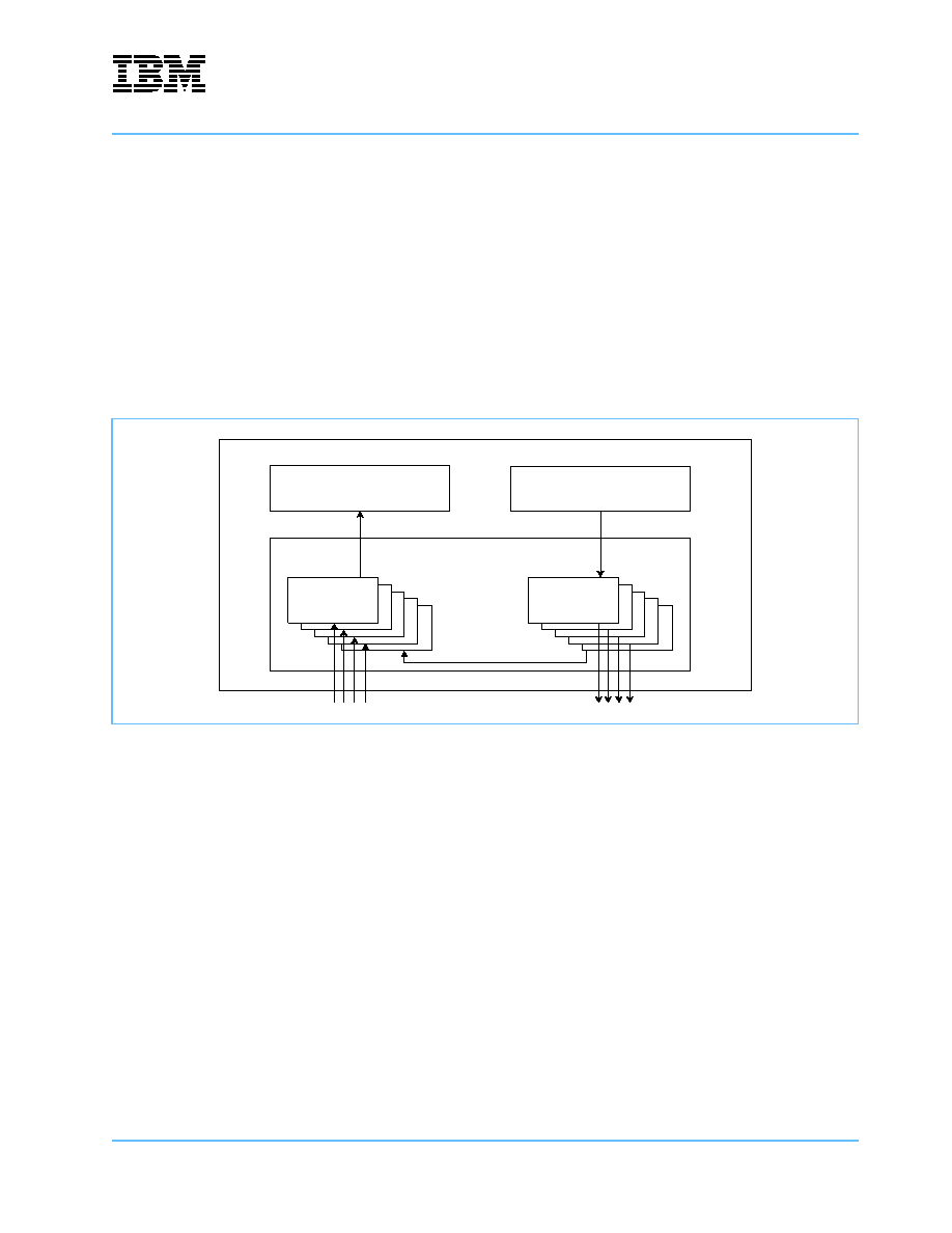
IBM PowerNP NP4GS3
Preliminary
Network Processor
np3_ds_sec03_pmm.fm.11
January 29, 2003
Physical MAC Multiplexer
Page 113 of 605
3. Physical MAC Multiplexer
The Physical MAC Multiplexer (PMM) moves data between physical layer devices and the network
processor. The PMM interfaces with the network processor's external ports in the ingress (I-PMM) and
egress (E-PMM) directions.
The PMM includes five Data Mover Units (DMUs), as illustrated in Figure 3-1. Four DMUs (A, B, C, and D)
can each be independently configured as an Ethernet Medium Access Control (MAC) or a packet over
SONET (POS) MAC. The device keeps a complete set of performance statistics on a per-port basis in either
mode. Each DMU moves data at 1 Gigabit per second (Gbps) in both the ingress and the egress directions.
The Wrap DMU enables traffic generated by the NP4GS3's egress side to move to the ingress side of the
device and up to the switch fabric.
Figure 3-1. PMM Overview
W
D
C
B
NP4GS3
Ingress EDS
DMU
A
B
C
D
PMM
W
Egress EDS
DMU
A
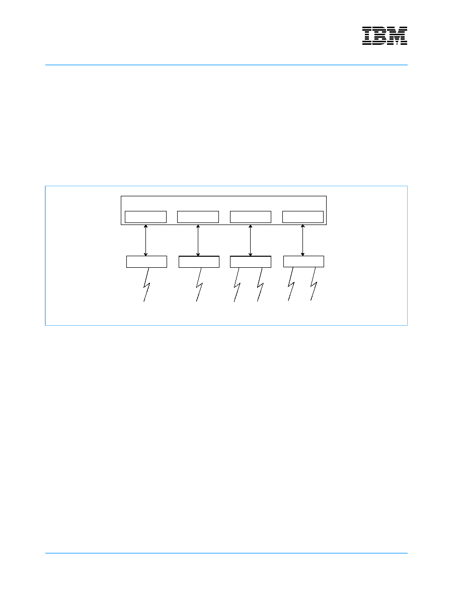
IBM PowerNP NP4GS3
Network Processor
Preliminary
Physical MAC Multiplexer
Page 114 of 605
np3_ds_sec03_pmm.fm.11
January 29, 2003
3.1 Ethernet Overview
A DMU configured in Ethernet mode can support either one port of Gigabit Ethernet or ten ports of Fast (10/
100) Ethernet. When in Gigabit Ethernet mode, each DMU can be configured with either a Gigabit Media-
Independent Interface (GMII) or a Ten-Bit Interface (TBI). When in Fast Ethernet mode, each DMU can be
configured with a Serial Media-Independent Interface (SMII). In this mode, the single DMU MAC can be
configured as ten ports. Each of these four DMUs can be configured in any of the Ethernet operation modes.
Figure 3-2: Ethernet Mode on page 114 shows a sample NP4GS3 with the PMM configured for Ethernet
interfaces. DMUs A and B are configured as Gigabit Ethernet MACs. DMUs C and D are configured as Fast
Ethernet MACs.
Figure 3-2. Ethernet Mode
DMU - A
NP4GS3
PHY
GMII or
TBI
1 Gigabit
Ethernet Port
DMU - B
PHY
1 Gigabit
Ethernet Port
DMU - C
PHY
DMU - D
PHY
SMII
SMII
Up to Ten
Fast Ethernet Ports
GMII or
TBI
Up to Ten
Fast Ethernet Ports

IBM PowerNP NP4GS3
Preliminary
Network Processor
np3_ds_sec03_pmm.fm.11
January 29, 2003
Physical MAC Multiplexer
Page 115 of 605
3.1.1 Ethernet Interface Timing Diagrams
The following figures show timing diagrams for the Ethernet interfaces:
� Figure 3-3: SMII Timing Diagram on page 115
� Figure 3-4: GMII Timing Diagram on page 115
� Figure 3-5: TBI Timing Diagram on page 116
� Figure 3-6: GMII POS Mode Timing Diagram on page 117.
Figure 3-3. SMII Timing Diagram
Figure 3-4. GMII Timing Diagram
Clock
Sync
Rx
CRS
RX_DV
RXD0
RXD1
RXD2
RXD3
RXD4
RXD5
RXD6
RXD7
CRS
TX_ER
TX_EN
TXD0
TXD1
TXD2
TXD3
TXD4
TXD5
TXD6
TXD7
TX_ER
Tx
RX_CLK
RX_DV
RXD<7:0>
RX_ER
FCS
preamble
SFD
Receive
TX_CLK
TX_EN
TXD<7:0>
TX_ER
FCS
preamble
Transmit

IBM PowerNP NP4GS3
Network Processor
Preliminary
Physical MAC Multiplexer
Page 116 of 605
np3_ds_sec03_pmm.fm.11
January 29, 2003
Figure 3-5. TBI Timing Diagram
T
R
I
TX_CLK
TX_EN
TXD[7:0]
TX_ER
FCS
preamble
TX Code Group
I = Idle
S = Start of Packet
D = Data
T = End of Packet (part 1)
R = End of Packet (part 2 or 3)
I
S
D
D
D
D
D
D
D
D
D
D
D
D
D
D
RX_CLK1
2.0 V
Rx_Code_Group[9:0]
1.4 V
0.8 V
RX_CLK0
t
HOLD
COMMA
Code-group
Valid
Data
t
SETUP
t
HOLD
t
SETUP
Receive Clocks and Receive Data
Transmit Data

IBM PowerNP NP4GS3
Preliminary
Network Processor
np3_ds_sec03_pmm.fm.11
January 29, 2003
Physical MAC Multiplexer
Page 117 of 605
3.1.2 Ethernet Counters
The NP4GS3 provides 36 Ethernet statistics counters per MAC (up to one million software-defined, hard-
ware-assisted counters), enabling support of many standard Management Information Bases (MIBs) at wire
speed.
Table 3-1: Ingress Ethernet Counters on page 118 and Table 3-2: Egress Ethernet Counters on page 119
show the statistics counters kept in each DMU when it operates in Ethernet mode. These counters are acces-
sible through the Control Access Bus (CAB) interface.
Figure 3-6. GMII POS Mode Timing Diagram
Rx_Data
Receive Valid Byte
Tx_Data
Transmit Byte Credit
valid
skip byte
do not send
ok to send
valid
valid
valid
do not send
ok to send
ok to send
Transmit Valid Byte

IBM PowerNP NP4GS3
Network Processor
Preliminary
Physical MAC Multiplexer
Page 118 of 605
np3_ds_sec03_pmm.fm.11
January 29, 2003
Table 3-1. Ingress Ethernet Counters
(Page 1 of 2)
Name / Group
Counter
No.
Group
Description
Notes
Short Frames
x`00'
Total number of frames received that were less than 64 octets long and were other-
wise well-formed (had a good CRC)
1, 2
Fragments
x`01'
Total number of frames received that were less than 64 octets long and had a bad
CRC
1, 2
Frames Received
(64 octets)
x`02'
Total number of frames (including bad frames) received that were 64 octets in length
1, 2
Frames Received
(65 to 127 octets)
x`03'
Total number of frames (including bad frames) received that were between 65 and
127 octets in length inclusive
1, 2
Frames Received
(128 to 255 octets)
x`04'
Total number of frames (including bad frames) received that were between 128 and
255 octets in length inclusive
1, 2
Frames Received
(256 to 511 octets)
x`05'
Total number of frames (including bad frames) received that were between 256 and
511 octets in length inclusive
1, 2
Frames Received
(512 to 1023 octets)
x`06'
Total number of frames (including bad frames) received that were between 512 and
1023 octets in length inclusive
1, 2
Frames Received
(1024 to 1518 octets)
x`07'
Total number of frames (including bad frames) received that were between 1024 and
1518 octets in length inclusive
1, 2
Jumbo Frames
x`14'
Total number of frames (including bad frames) received with a length between 1519
octets and the configured maximum length of a jumbo frame, or between 1519
octets and configured maximum length of a jumbo frame plus 4 if VLAN is asserted.
4
Long Frames Received
x`08'
4
Total number of long frames received with a good CRC that were either:
1)
Longer than 1518 octets (excluding framing bits, but including CRC octets), and
were otherwise well-formed (good CRC), VLAN and Jumbo deasserted
2)
VLAN frames that were longer than 1522 octets, with Jumbo deasserted
3)
Jumbo frames that were longer than the configured maximum length of a jumbo
frame in octets, with VLAN deasserted
4)
Jumbo VLAN frames that were longer than the configured maximum length
of a jumbo frame plus 4 in octets
3, 4
Jabber
x`09'
Total number of long frames received with bad CRC that were either:
1)
Longer than 1518 octets (excluding framing bits, but including CRC octets), and
were not well-formed (Bad CRC), VLAN and Jumbo not asserted
2)
VLAN frames that were longer than 1522 octets, with Jumbo deasserted
3)
Jumbo frames that were longer than the configured maximum length of a jumbo
frame in octets, with VLAN deasserted
4)
Jumbo VLAN frames that were longer than the configured maximum length of a
jumbo frame plus 4 in octets
3, 4
Frames with Bad CRC
x`0A'
Total number of frames received that were not long frames, but had bad CRC
2
Unicast Frames
Received
x`0B'
Total number of good frames received that were directed to the unicast address
(excluding multicast frames, broadcast frames, or long frames)
Broadcast Frames
Received
x`0C'
3
Total number of good frames received that were directed to the broadcast address
(excluding multicast frames or long frames)
1. The states of VLAN or Jumbo have no effect on this count.
2. Excluding framing bits but including CRC octets
3. Reception of frames meeting the criteria for this counter are aborted by the hardware. Abort is indicated in the Ingress Port Control
Block and in the Ingress Frame Control Block. If the frame has not been forwarded by the picocode, the picocode must enqueue the
frame to the ingress discard queue. If the frame has been forwarded, then the egress hardware will discard the frame. Further
reception at the MAC is inhibited until the next frame starts.
4. For NP4GS3C (R3.x) the maximum length of a jumbo frame is determined by the value in the Ethernet Jumbo Frame Size register
(see Section 13.27 beginning on page 536). For NP4GS3B (R2.0), the maximum length of a jumbo frame is fixed at a value of 9018
bytes.

IBM PowerNP NP4GS3
Preliminary
Network Processor
np3_ds_sec03_pmm.fm.11
January 29, 2003
Physical MAC Multiplexer
Page 119 of 605
Multicast Frames
Received
x`0D'
Total number of good frames received that were directed to the multicast address
(excluding broadcast frames, or long frames)
Total Frames Received
x`0E'
Total number of frames (including bad frames, broadcast frames, multicast frames,
unicast frames, and long frames) received
Receive Errors
x`0F'
Total number of frames received in which the PHY detected an error and asserted
the Rx_Err signal
Overruns
x`13'
2
Total number of frames received when the PMM internal buffer was full and the
frame couldn't be stored. Includes frames in the process of being received when the
PMM internal buffer becomes full.
Pause Frames
x`10'
Total number of MAC pause frames received that were well-formed and had a good
CRC
Total Pause Time
x`11'
1
Total amount of time spent in a pause condition as a result of receiving a good pause
MAC frame
Total Octets Received
x`12'
0
Total number of octets of data (including those in bad frames) received on the net-
work
2
Table 3-2. Egress Ethernet Counters
(Page 1 of 3)
Name
Counter
No.
Group
Description
Cnt
Short Frames
x`00'
Total number of frames transmitted with less than 64 octets that had good CRC.
1, 2
Runt Frames (Bad CRC)
x`01'
Total number of frames transmitted with less than 64 octets that had bad CRC.
1, 2
Frames Transmitted
(64 octets)
x`02'
Total number of frames (including bad frames) transmitted that were 64 octets
in length.
1
Frames Transmitted
(65 to 127 octets)
x`03'
Total number of frames (including bad frames) transmitted that were between
65 and 127 octets in length inclusive.
1, 3
Frames Transmitted
(128 to 255 octets)
x`04'
Total number of frames (including bad frames) transmitted that were between
128 and 255 octets in length inclusive
1, 3
Frames Transmitted
(256 to 511 octets)
x`05'
Total number of frames (including bad frames) transmitted that were between
256 and 511 octets in length inclusive.
1, 3
Frames Transmitted
(512 to 1023 octets)
x`06'
Total number of frames (including bad frames) transmitted that were between
512 and 1023 octets in length inclusive.
1, 3
1. The states of VLAN or Jumbo have no effect on this count.
2. Including the frame type byte.
3. Excluding framing bits but including CRC octets.
4. For NP4GS3C (R3.x) the maximum length of a jumbo frame is determined by the value in the Ethernet Jumbo Frame Size register
(see Section 13.27 beginning on page 536). For NP4GS3B (R2.0), the maximum length of a jumbo frame is fixed at a value of
9018 bytes.
Table 3-1. Ingress Ethernet Counters
(Page 2 of 2)
Name / Group
Counter
No.
Group
Description
Notes
1. The states of VLAN or Jumbo have no effect on this count.
2. Excluding framing bits but including CRC octets
3. Reception of frames meeting the criteria for this counter are aborted by the hardware. Abort is indicated in the Ingress Port Control
Block and in the Ingress Frame Control Block. If the frame has not been forwarded by the picocode, the picocode must enqueue the
frame to the ingress discard queue. If the frame has been forwarded, then the egress hardware will discard the frame. Further
reception at the MAC is inhibited until the next frame starts.
4. For NP4GS3C (R3.x) the maximum length of a jumbo frame is determined by the value in the Ethernet Jumbo Frame Size register
(see Section 13.27 beginning on page 536). For NP4GS3B (R2.0), the maximum length of a jumbo frame is fixed at a value of 9018
bytes.

IBM PowerNP NP4GS3
Network Processor
Preliminary
Physical MAC Multiplexer
Page 120 of 605
np3_ds_sec03_pmm.fm.11
January 29, 2003
Frames Transmitted
(1024 to 1518 octets)
x`07'
Total number of frames (including bad frames) transmitted that were between
1024 and 1518 octets in length inclusive.
1, 3
Jumbo Frames
x`16'
Total number of frames (including bad frames) transmitted with a length
between 1519 octets and the configured maximum length of a jumbo frame, or
between 1519 octets and configured maximum length of a jumbo frame plus 4 if
VLAN is asserted. If Jumbo is not asserted, the frame is a long frame.
4
Long Frames Transmitted
x`08'
4
Total number of frames with good CRC transmitted that were either:
1)
Longer than 1518 octets (excluding framing bits, but including CRC
octets), and were otherwise well-formed (good CRC), VLAN and Jumbo
are deasserted
2)
VLAN frames that were longer than 1522 octets with Jumbo deasserted
3)
Jumbo frames that were longer than the configured maximum length of a
jumbo frame in octets with Jumbo deasserted
4)
Jumbo VLAN frames that were longer than the configured maximum
length of a jumbo frame plus 4 in octets
4
Jabber
x`09'
Total number of frames with bad CRC transmitted that were either:
1)
Longer than 1518 octets (excluding framing bits, but including CRC
octets), and were otherwise well-formed (good CRC), VLAN and Jumbo
are deasserted
2)
VLAN frames that were longer than 1522 octets with Jumbo deasserted
3)
Jumbo frames that were longer than the configured maximum length of a
jumbo frame in octets with Jumbo deasserted
4)
Jumbo VLAN frames that were longer than the configured maximum
length of a jumbo frame plus 4 in octets
4
Late Collisions
x`0A'
Total number of frames transmitted that experienced a network collision after
64 bytes of the frame had been transmitted.
1
Total Collisions
x`0B'
3
Best estimate of the total number of collisions on this Ethernet segment
1
Single Collisions
x`0C'
Total number of frames transmitted that experienced one collision before 64
bytes of the frame were transmitted on the network
1
Multiple Collisions
x`0D'
Total number of frames transmitted that experienced more than one collision
before 64 bytes of the frame were transmitted on the network
1
Excessive Deferrals
x`0E'
Total number of frames whose transmission could not be started before the
deferral time out expired. The deferral time out value is 24,416 media bit times.
1
Underruns
x`0F'
Total number of frames that were not completely transmitted because the data
could not be obtained from the Egress EDS fast enough to maintain the media
data rate
Aborted Frames
x`17'
Total number of frames that had one of the following errors:
- link pointer parity errors,
- header QSB field specification which point beyond the end of frame,
- Invalid BCI specification
When one of these errors occurs, the frame transmission is aborted by the
Egress PMM and the event is counted. Information about the event is recorded
in the Aborted Frame Error Indicator register.
When an Invalid BCI specification is detected, twins associated with the frame
are not returned to the free queue.
Table 3-2. Egress Ethernet Counters
(Page 2 of 3)
Name
Counter
No.
Group
Description
Cnt
1. The states of VLAN or Jumbo have no effect on this count.
2. Including the frame type byte.
3. Excluding framing bits but including CRC octets.
4. For NP4GS3C (R3.x) the maximum length of a jumbo frame is determined by the value in the Ethernet Jumbo Frame Size register
(see Section 13.27 beginning on page 536). For NP4GS3B (R2.0), the maximum length of a jumbo frame is fixed at a value of
9018 bytes.

IBM PowerNP NP4GS3
Preliminary
Network Processor
np3_ds_sec03_pmm.fm.11
January 29, 2003
Physical MAC Multiplexer
Page 121 of 605
CRC Error
x`10'
2
Total number of frames transmitted that had a legal length (excluding framing
bit, but including CRC octets) of between 64 and 9018 octets, (64 and 9022 for
VLAN frames) inclusive, but had a bad CRC
Excessive Collisions
x`11'
Total number of frames that experienced more than 16 collisions during trans-
mit attempts. These frames are dropped and not transmitted
Unicast Frames
Transmitted
x`12'
Total number of good frames transmitted that were directed to the unicast
address (not including multicast frames or broadcast frames)
Broadcast Frames
Transmitted
x`13'
Total number of good frames transmitted that were directed to the broadcast
address (not including multicast frames)
Multicast Frames
Transmitted
x`14'
Total number of good frames transmitted that were directed to the multicast
address (not including broadcast frames)
Total Octets Transmitted
x`15'
0
Total number of octets of data (including those in bad frames) transmitted on
the network
3
Table 3-2. Egress Ethernet Counters
(Page 3 of 3)
Name
Counter
No.
Group
Description
Cnt
1. The states of VLAN or Jumbo have no effect on this count.
2. Including the frame type byte.
3. Excluding framing bits but including CRC octets.
4. For NP4GS3C (R3.x) the maximum length of a jumbo frame is determined by the value in the Ethernet Jumbo Frame Size register
(see Section 13.27 beginning on page 536). For NP4GS3B (R2.0), the maximum length of a jumbo frame is fixed at a value of
9018 bytes.

IBM PowerNP NP4GS3
Network Processor
Preliminary
Physical MAC Multiplexer
Page 122 of 605
np3_ds_sec03_pmm.fm.11
January 29, 2003
3.1.3 Ethernet Support
Table 3-3 lists the features and standards supported by a DMU in the different Ethernet modes.
Table 3-3. Ethernet Support
Feature
DMU Bus Mode
10/100
Ethernet
SMII
Gigabit
Ethernet
GMII
Gigabit
Ethernet
TBI
Compatible with IEEE 802.3
, 2000.
X
X
X
Compliant with RFC 1757 Management Registers and Counters (Tx/Rx Counters)
Additional receive counters for total number of pause frames and total aggregate pause time
Additional transmit counters for number of single collisions and number of multiple collisions
X
X
X
Supports the IEEE standards on flow control by honoring received pause frames and inhibiting frame
transmission while maintaining pause counter statistics
X
X
X
Supports SMII to the PHY
Interfaces with up to ten PHYs that support the SMII interface. Each of the ten interfaces can
have a bit rate of either 10 Mbps or 100 Mbps.
X
Capable of handling ten ports of 10 Mbps or 100 Mbps media speeds, any speed mix
X
Supports half-duplex operations at media speed on all ports
X
Supports Binary Exponential Back-off (BEB) compliant with the IEEE 802.3: 1993 (E)
X
Supports full duplex point-to-point operations at media speed
X
X
X
Detects VLAN (8100 frame type) Ethernet frames and accounts for them when calculating long frames
X
X
X
Supports two Ethernet frame types (programmable) and, based on these, detects received frames
with a type field that matches one of those types. A match instructs the Multi-port 10/100 MAC to strip
the DA, SA, and Type fields from the received frame and to instruct the higher device functions to
queue the frame in a different queue.
An example of a special function is to identify Ethernet encapsulated guided frames. A mismatch
results in normal frame queueing and normal higher device processing.
X
X
X
Programmable cyclic redundancy check (CRC) Insertion on a frame basis
With CRC Insertion disabled, MAC transmits frames as is (suitable for switch environments)
With CRC Insertion enabled, the MAC calculates and inserts the CRC
X
X
X
Includes jumbo frame support. When configured, can transmit and receive up to the configured maxi-
mum length of a jumbo frame in octets. This is increased by plus 4 octets when a VLAN tagged frame
is detected.
For NP4GS3C (R3.x) the maximum length of a jumbo frame is determined by the value in the Ethernet
Jumbo Frame Size register (see Section 13.27 beginning on page 536). For NP4GS3B (R2.0), the
maximum length of a jumbo frame is fixed at a value of 9018 bytes.
X
X
X
Supports the IBM Rx_Byte_Valid and Tx_Byte_Credit signals.
X
Can be combined with the TBI to form a complete TBI solution.
X
Interfaces with any PMA/PMI physical layer using the PMA service interface defined in the IEEE 802.3
standard
X
Synchronizes the data received from the PMA (two phase) clock with the MAC (single phase) clock.
Provides a signal to the MAC indicating those clock cycles that contain new data.
X
Checks the received code groups (10 bits) for commas and establishes word synchronization
X
Calculates and checks the TBI running disparity
X
Supports auto-negotiation including two next pages
X

IBM PowerNP NP4GS3
Preliminary
Network Processor
np3_ds_sec03_pmm.fm.11
January 29, 2003
Physical MAC Multiplexer
Page 123 of 605
3.2 POS Overview
A DMU configured in packet over Sonet (POS) mode can support both clear-channel and channelized Optical
Carrier (OCs) interfaces. A DMU can support the following types and speeds of POS framers: OC-3c, OC-12,
OC-12c, OC-48, and OC-48c.
Each DMU allows connection to OC-3c, OC-12, or OC-12c framers. To provide an OC-48 link, all four DMUs
must be attached to a single framer with each DMU providing four OC-3c channels or one OC-12c channel to
the framer. To provide an OC-48 clear channel (OC-48c) link, DMU A must be configured to attach to a 32-bit
framer and the other three DMUs, although configured for OC-48 mode, are disabled except for their interface
pins.
Table 3-4 shows the three DMU configuration modes: OC-3c, OC-12c, and OC-48c. When configured for
OC-3c, the DMU assumes that it must poll the four possible attached ports before transferring data. If the
DMU is configured for either OC-12c or OC-48c, the DMU does not poll the framer.
Figure 3-7 shows a configuration in which the PMM has OC-3c, OC-12, and OC-12c connections operating
simultaneously. Each of the four DMUs has been configured to operate as single port or as four ports. Each
of the four DMUs supports an 8-bit data interface in both the ingress and egress directions.
Table 3-4. DMU and Framer Configurations
DMU Configuration Mode
Networks Supported via POS Framer
OC-3c (8-bit mode)
4 x OC-3c per DMU or
1 x OC-12c per DMU
1 x OC-48c (all 4 DMUs required)
OC-12c (8-bit mode)
1 x OC-12c per DMU or
1 x OC-48c (all 4 DMUs required)
OC-48c (32-bit mode)
1 x OC-48c (DMU A in 32-bit mode)
Figure 3-7. OC-3c / OC-12 / OC-12c Configuration
Framer
Framer
Framer
Framer
4 x OC-3c
Connections
OC-12c
OC-12
4 x OC-3c
Connections
4 Ports
DMU - A
NP4GS3
DMU - B
DMU - C
DMU - D
4 Ports
4 Ports
1 Port
Connection Connection
OC-3c mode
OC-3c mode
OC-12c mode
OC-3c mode
4 x Logical
Channels
4 x Logical
Channels
4 x Logical
Channels
1 x Logical
Channels

IBM PowerNP NP4GS3
Network Processor
Preliminary
Physical MAC Multiplexer
Page 124 of 605
np3_ds_sec03_pmm.fm.11
January 29, 2003
Figure 3-8 shows an example of an OC-48 configuration. Each DMU can be configured to operate in a single-
port mode or in a multiport polling mode. The single-port mode supports an OC-12c channel, and the multi-
port polling mode supports four OC-3c channels. Each DMU supports an 8-bit data interface in both the
ingress and egress directions.
-
Figure 3-9 shows an OC-48c configuration. DMU A is configured to operate in a single-port 32-bit mode to
support OC-48c. DMUs B, C, and D must be configured for OC-48 mode and their data ports routed to DMU
A. Except for the I/Os, DMUs B, C, and D are not used in this configuration. The attached framer must also be
configured for a 32-bit data interface.
Figure 3-8. OC-48 Configuration
Figure 3-9. OC-48c Configuration
Framer
OC-48
Connection
4 Ports
DMU - A
NP4GS3
DMU - B
DMU - C
DMU - D
1 Port
4 Ports
1 Port
OC-3c mode
OC-12c mode
OC-12c mode
OC-3c mode
4
� OC-3c
channels
4
� OC-3c
channels
1
� OC-12c
channel
DMU - A
DMU - B
DMU - C
Framer
OC-48c
Connection
1 Port
NP4GS3
DMU - D
OC-48c mode
OC-48 mode
OC-48 mode
OC-48 mode

IBM PowerNP NP4GS3
Preliminary
Network Processor
np3_ds_sec03_pmm.fm.11
January 29, 2003
Physical MAC Multiplexer
Page 125 of 605
3.2.1 POS Timing Diagrams
The following figures show timing diagrams for the different POS modes:
� OC-3c
- Figure 3-10: Receive POS8 Interface Timing for 8-bit Data Bus (OC-3c) on page 125
- Figure 3-11: Transmit POS8 Interface Timing for 8-bit Data Bus (OC-3c) on page 126
� OC-12c
- Figure 3-12: Receive POS8 Interface Timing for 8-bit Data Bus (OC-12c) on page 126
- Figure 3-13: Transmit POS8 Interface Timing for 8-bit Data Bus (OC-12c) on page 127
� OC-48c
- Figure 3-14: Receive POS32 Interface Timing for 32-bit Data Bus (OC-48c) on page 127
- Figure 3-15: Transmit POS32 Interface Timing for 32-bit Data Bus (OC-48c) on page 128
Figure 3-10. Receive POS8 Interface Timing for 8-bit Data Bus (OC-3c)
RxClk
RxEOF
RxVAL
RxData
RxENB
RxAddr
RxPFA
1
2
3
4
5
6
7
8
9
10
11
12
13
14
15
16
17
18
19
20
0
P
1
P
2
P
3
P
0
P
1
P
2
DP
2
DP
0
DP
0
DP
0
DP
0
DP
0
DP
0
DP
0
P
3
P
0
P
2
P
3
P
0
P
1
P
2
P
3
P
0
P
1
P
2
P
3
P
0
P
1
P
2
XX
XX
XX
XX
21
DP
2
XX
XX
1. Data is being received from port #0 while the DMU is polling.
2. In clock cycle #3 the framer asserts RxPFA indicating data is available. In this example the DMU is configured for two
cycles of framer latency (bus_delay = 1), therefore it is port #2 responding with RxPFA (clock cycle #1).
3. In clock cycle #6 the DMU deasserts RxENB (negative active) to indicate it is starting the port selection process.
4. In clock cycle #8 the DMU puts P
2
on RxAddr.
5. In clock cycle #9 the DMU selects port P
2
by asserting RxENB. The port selected is the port whose address is on RxA-
ddr the cycle before RxENB is asserted.
6. In clock cycle #16 the framer deasserts RxVAL (assumed that the framer was not ready to continue data transfer) and
restarts data transfer to the DMU during clock cycle #17.
7. In clock cycle #18 the framer asserts RxEOF marking the last transfer for the frame.
8. In clock cycle #19 the framer deasserts both RxEOF and RxVAL completing the frame transfer.
9. In clock cycle #16 and #17 RxPFA is asserted indicating data is available on ports 0 and 1.
10. In clock cycle #20 the DMU starts the selection of the next port.
DP
0
DP
2
XX DP
2
DP
2
DP
2
DP
2
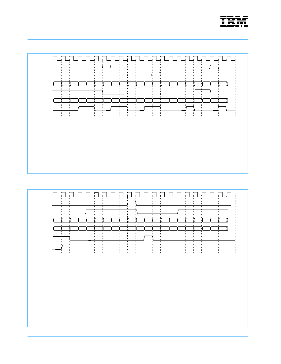
IBM PowerNP NP4GS3
Network Processor
Preliminary
Physical MAC Multiplexer
Page 126 of 605
np3_ds_sec03_pmm.fm.11
January 29, 2003
Figure 3-11. Transmit POS8 Interface Timing for 8-bit Data Bus (OC-3c)
Figure 3-12. Receive POS8 Interface Timing for 8-bit Data Bus (OC-12c)
TxClk
TxSOF
TxEOF
TxData
TxENB
TxAddr
TxPFA
1
2
3
4
5
6
7
8
9
10
11
12
13
14
15
16
17
18
19
20
0
P
1
P
2
P
3
P
0
P
1
P
2
DP
2
P
3
P
0
P
1
P
2
P
3
P
0
P
1
P
2
P
3
P
0
P
1
P
2
P
3
P
0
P
1
XX
XX
21
DP
2
1. In this figure it is assumed that the framer has a 2-cycle delay before responding to the DMU and that the DMU
has bus_delay = 1.
2. In clock cycle #3 the framer responds to the Poll by asserting TxPFA, this indicates that the FIFO for ports 2 and
3 have room for data (2 clock cycle delay).
3. In clock cycle #6 the DMU starts transferring a new frame to port 2 by asserting TxSOF, asserting TxENB (nega-
tive active), and putting data on TxData.
4. In clock cycle #12 the DMU asserts TxEOF indicating the last transfer of the frame.
5. In clock cycle #13 the DMU deasserts TxENB to indicate that the DMU is in the port selection process.
6. In clock cycle #16 the framer asserts TxPFA indicating it has data for port 3.
7. In clock cycle #19 the DMU asserts TxENB and selects port 3.
8. In clock cycle #19 the DMU asserts TxSOF indicating the start of a new frame for port 3 and places data on
TxData.
DP
2
XX
DP
2
DP
3
XX
XX
XX
XX
XX
XX DP
2
DP
2
XX
XX
XX
DP
3
DP
2
RxClk
RxEOF
RxVAL
RxData
RxAddr
RxPFA
1
2
3
4
5
6
7
8
9
10
11
12
13
14
15
16
17
18
19
20
0
P
0
P
0
P
0
P
0
P
0
P
0
XX
P
0
P
0
P
0
P
0
P
0
P
0
P
0
P
0
P
0
P
0
P
0
P
0
P
0
P
0
P
0
Data Data
21
Data
1. In clock cycle #1 the framer asserts RxPFA indicating it has data to transfer to the DMU (for OC-12c operation
the framer can tie RxPFA to a logical 1 and control data transfers with RxVAL).
2. In clock cycle #2 the DMU asserts RxENB (negative active) selecting the port whose address was on RxAddr
during clock cycle #1 (for OC-12c operation the DMU must provide RxAddr from the card).
3. In clock cycle #4 the framer asserts RxVAL and starts the data transfer to the DMU. Data transfer continues as
long as RxVAL is asserted. The framer must deassert RxVAL at the end of the frame, clock cycle #10, but can
deassert and then reassert anytime within the frame.
4. In clock cycle #11 the DMU deasserts RxENB in response to RxEOF being asserted at clock cycle #9.
5. In clock cycle #12 the DMU asserts RxENB in response to RxPFA being asserted.
6. In clock cycle #15 the framer starts the transfer of the next frame by asserting RxVAL. The DMU accepts data as
early as clock cycle #12 and will wait (no limit) until the framer asserts RxVAL before accepting data.
7. The framer can control data transfer using RxVAL and the DMU can control data transfer using RxENB. As noted
above, RxPFA can remain asserted.
Data
Data
XX
Data
XX
XX
XX XX
Data Data Data Data
Data
XX
XX
Data
XX
RxENB
Note: For OC-12c, RxAddr is not provided by the DMU. RxAddr must be provided by board logic. There is a two cycle delay
between the assertion of RxENB and RxVAL, the DMU can be configured to accept a one cycle delay.
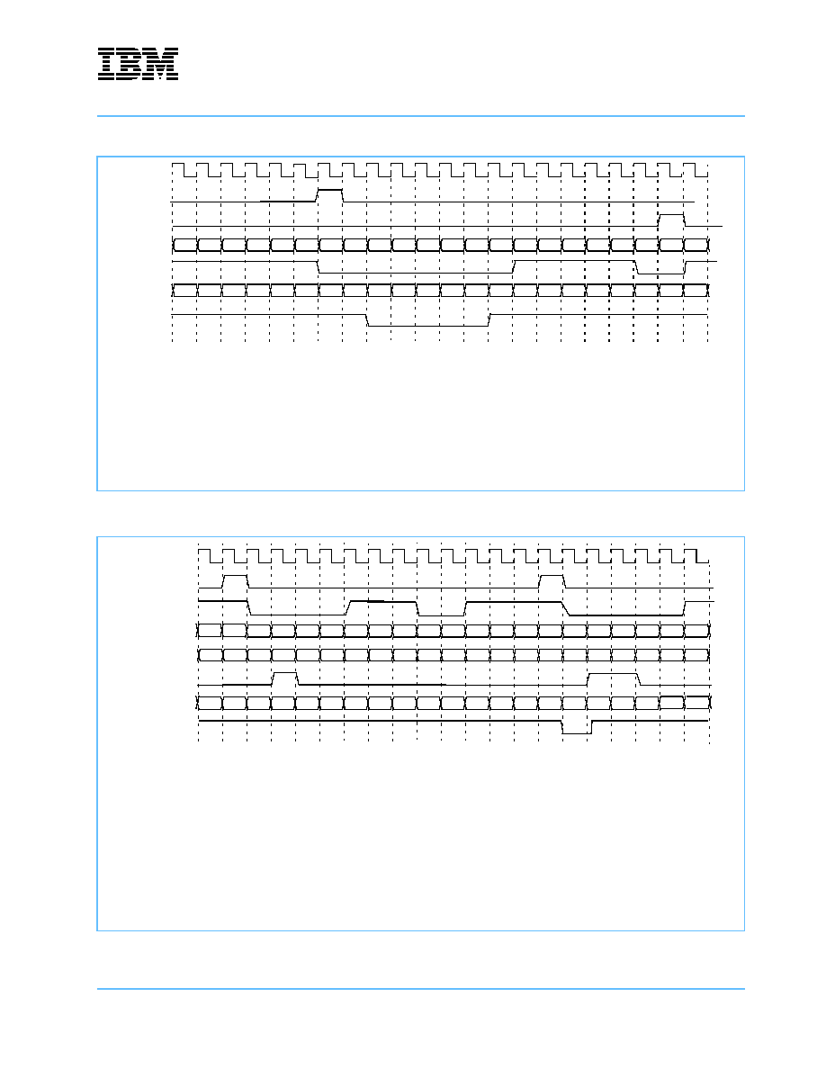
IBM PowerNP NP4GS3
Preliminary
Network Processor
np3_ds_sec03_pmm.fm.11
January 29, 2003
Physical MAC Multiplexer
Page 127 of 605
Figure 3-13. Transmit POS8 Interface Timing for 8-bit Data Bus (OC-12c)
Figure 3-14. Receive POS32 Interface Timing for 32-bit Data Bus (OC-48c)
TxClk
TxSOF
TxEOF
TxData
TxAddr
TxPFA
1
2
3
4
5
6
7
8
9
10
11
12
13
14
15
16
17
18
19
20
0
P
0
P
0
P
0
XX
P
0
P
0
P
0
P
0
P
0
P
0
P
0
P
0
P
0
P
0
P
0
P
0
P
0
P
0
P
0
XX
XX
21
DP
0
1. In clock cycle #0 the framer has TxPFA asserted indicating it can accept data from the DMU.
2. In clock cycle #6 the DMU selects port 0 by asserting TxENB (negative active). The DMU also asserts TxSOF
indicating the beginning of the frame and places data on TxData.
3. In clock cycle #8 the framer indicates it can not accept more data by deasserting TxPFA. The DMU requires 6
clock cycles to stop data transfer, hence data transfer stops after clock cycle #13 by deasserting TxEnb.
4. In clock cycle # 15 the framer asserts TxPFA indicating that it can accept more data.
5. In clock cycle #19 the DMU asserts TxENB indicating data is valid on TxData.
6. In clock cycle #20 the DMU asserts TxEOF indicating the last transfer of the frame.
7. In clock cycle #21 the DMU deasserts TxEOF and TxENB.
DP
0
XX
DP
0
DP
0
XX
XX
XX
DP
0
DP
0
DP
0
DP
0
DP
0
XX
DP
0
TxENB
Note: For OC-12c, TxAddr is not provided by the DMU. TxAddr must be provided by board logic.
XX
XX
XX
XX
P
0
P
0
P
0
P
0
RxClk
RxEOF
RxVAL
RxData
RxENB
RxPadL
RxPFA
1
2
3
4
5
6
7
8
9
10
11
12
13
14
15
16
17
18
19
20
0
0
3
0
0
Word
Word
Word
Word Word
XXXX
XXXX
XXXX
XXXX
XXXX
0
0
0
0
0
0
0
0
0
0
1
0
0
0
0
XXXX
XXXX
Word
Word
Word
XXXX
XXXX
XXXX
XXXX
Word
Word
0
0
RxAddr
P
0
P
0
P
0
Note: For OC-48c, RxAddr is not provided by the DMU. RxAddr must be provided by board logic. This figure shows a two clock
1. In clock cycle #0 the DMU is receiving data from the framer.
2. In clock cycle #1 the framer asserts RxEOF indicating the last data transfer of the current frame.
3. In clock cycle #2 the framer deasserts RxEOF and RxVal marking the end of the frame.
4. In clock cycle #3 the DMU deasserts RxENB starting the port selection process.
5. In clock cycle #4 the DMU checks RxPFA (asserted) and asserts RxENB indicating it can accept more data.
6. In clock cycle #6 the data transfer from the framer to the DMU is started. The data transfer continues until clock cycle #15.
The framer halts the transfer during cycles 9 and 10 by deasserting RxVal.
7. In clock cycle #14 the framer asserts RxEOF marking the end of the frame.
8. In clock cycle #16 the DMU deasserts RxENB. The DMU asserts RxENB in clock cycle #18 after detecting RxPFA asserted,
indicating that the framer has data to transfer. Assertion of RxENB in clock cycle #18 selects port 0 again and data transfer
begins in clock cycle #20.
P
0
P
0
P
0
P
0
P
0
P
0
P
0
P
0
P
0
P
0
P
0
P
0
P
0
P
0
P
0
P
0
P
0
P
0
cycle delay between deassertion of RxEnb and the assertion of RxVal. The DMU can be configured to accept a one cycle delay.

IBM PowerNP NP4GS3
Network Processor
Preliminary
Physical MAC Multiplexer
Page 128 of 605
np3_ds_sec03_pmm.fm.11
January 29, 2003
Figure 3-15. Transmit POS32 Interface Timing for 32-bit Data Bus (OC-48c)
TxClk
TxSOF
TxEOF
TxData
TxENB
TxPadL
TxPFA
0
0
0
0
Word Word Word XXXX
Word Word Word Word Word Word
0
0
0
0
0
0
2
0
0
0
1
0
0
0
0
XXXX XXXX Word Word Word XXXX XXXX XXXX XXXX XXXX XXXX
0
0
1
2
3
4
5
6
7
8
9
10
11
12
13
14
15
16
17
18
19
20
0
1. In clock cycle #2 the framer deasserts RxPFA, indicating it can not accept more data from the DMU.
2. In clock cycle #9 the DMU stops the data transfer in response to the deassertion of TxPFA in clock cycle #2.
3. In clock cycle #9 the DMU deasserts TxENB and begins its selection sequence.
4. In clock cycle #5 the framer asserts TxPFA indicating it can again accept data. Seven clock cycles later the DMU will assert
TxENB (clock cycle #12) and place the next data word on TxData.
5. In clock cycle #14 the DMU asserts TxEOF to indicate the end of the frame. The DMU also indicates the number of pad bytes
in the last data transfer (in this example 3 data bytes were set in the last data transfer).
6. In clock cycle #15 the DMU deasserts TxEOF and deasserts TxENB indicating the end of the frame.
7. In clock cycle #17 the framer deasserts TxPFA indicating that it can not accept more data.
Note: For OC-12c, TxAddr is not provided by the DMU. TxAddr must be provided by board logic.
TxAddr
P
0
P
0
P
0
P
0
P
0
P
0
P
0
P
0
P
0
P
0
P
0
P
0
P
0
P
0
P
0
P
0
P
0
P
0
P
0
P
0
P
0

IBM PowerNP NP4GS3
Preliminary
Network Processor
np3_ds_sec03_pmm.fm.11
January 29, 2003
Physical MAC Multiplexer
Page 129 of 605
3.2.2 POS Counters
Table 3-5 on page 129 and Table 3-6 on page 131 provide information about the counters maintained to
support POS interfaces.
Many of the counters defined in these tables deal with long frames. A long frame is a packet whose byte
count exceeds the value held in the packet over SONET Maximum Frame Size (POS_Max_FS) register (see
Configuration on page 459). The byte count includes the cyclic redundancy check (CRC) octets.
Reception of packets meeting the criteria for long frames is aborted by the hardware. Abort is indicated in the
Ingress Port Control Block and in the Ingress Frame Control Block. If the packet has not been forwarded by
the picocode, the picocode must enqueue the packet to the ingress discard queue. If the packet has been
forwarded, then the egress hardware will discard the frame. Further reception at the MAC is inhibited until the
next packet starts.
Table 3-5. Receive Counter RAM Addresses for Ingress POS MAC
(Page 1 of 2)
Port
Name
Counter Number
Description
Port 0
Long Frames Received
x`00'
Total number of frames received that were longer than the value
contained in the POS Maximum Frame Size Register
(POS_Max_FS) including CRC octets
Frames with Bad CRC
x`01'
Total number of frames received that had a length of the value
contained in the POS Maximum Frame Size Register
(POS_Max_FS) or less, but had a bad CRC
Total Good Frames Received
x`02'
Total number of frames (excluding frames with bad CRC, and long
frames) received
Receive Errors
x`03'
Total number of frames received in which the Framer detected an
error and asserted the Rx_Err signal
Total Octets Received
(including frames with errors)
x`10'
Total number of octets of data (including those in bad frames)
received on the network
Port 1
Long Frames Received
x`04'
Total number of frames received that were longer than the value
contained in the POS Maximum Frame Size Register
(POS_Max_FS) including CRC octets
Frames with Bad CRC
x`05'
Total number of frames received that had a length of the value
contained in the POS Maximum frame Size Register
(POS_Max_FS) or less, but had a bad CRC
Total Good Frames Received
x`06'
Total number of frames (excluding frames with a bad CRC, and
long frames) received
Receive Errors
x`07'
Total number of frames received in which the Framer detected an
error and asserted the Rx_Err signal
Total Octets Received
(including frames with errors)
x`11'
Total number of octets of data (including those in bad frames)
received on the network

IBM PowerNP NP4GS3
Network Processor
Preliminary
Physical MAC Multiplexer
Page 130 of 605
np3_ds_sec03_pmm.fm.11
January 29, 2003
Port 2
Long Frames Received
x`08'
Total number of frames received that were longer than the value
contained in the POS Maximum Frame Size Register
(POS_Max_FS) including CRC octets
Frames with Bad CRC
x`09'
Total number of frames received that had a length of the value
contained in the POS Maximum Frame Size Register
(POS_Max_FS) or less, but had a bad CRC
Total Good Frames Received
x`0A'
Total number of frames (excluding frames with a bad CRC, and
long frames) received
Receive Errors
x`0B'
Total number of frames received in which the Framer detected an
error and asserted the Rx_err signal
Total Octets Received
(including frames with errors)
x`12'
Total number of octets of data (including those in bad frames)
received on the network
Port 3
Long Frames Received
x`0C'
Total number of frames received that were longer than the value
contained in the POS Maximum Frame Size Register
(POS_Max_FS) including CRC octets
Frames with Bad CRC
x`0D'
Total number of frames received that had a length of the value
contained in the POS Maximum Frame Size Register
(POS_Max_FS) or less, but had a bad CRC
Total Good Frames Received
x`0E'
Total number of frames (excluding frames with a bad CRC, and
long frames) received
Receive Errors
x`0F'
Total number of frames received in which the Framer detected an
error and asserted the Rx_Err signal
Total Octets Received
(including frames with errors)
x`13'
Total number of octets of data (including those in bad frames)
received on the network
Table 3-5. Receive Counter RAM Addresses for Ingress POS MAC
(Page 2 of 2)
Port
Name
Counter Number
Description

IBM PowerNP NP4GS3
Preliminary
Network Processor
np3_ds_sec03_pmm.fm.11
January 29, 2003
Physical MAC Multiplexer
Page 131 of 605
Table 3-6. Transmit Counter RAM Addresses for Egress POS MAC
(Page 1 of 2)
Port
Name
Counter Number
Description
Port 0
Long Frames Transmitted
x`00'
Total number of frames transmitted that were longer than the value
contained in the POS Maximum Frame Size Register
(POS_Max_FS) including CRC octets
Frames with Bad CRC
x`01'
Total number of frames transmitted that had a length of the value
contained in the POS Maximum Frame Register (POS_Max_FS)
or less, but had bad CRC
Total Good Frames Transmitted
x`02'
Total number of frames (excluding frames with a bad CRC, and
long frames) transmitted
Transmit Underruns
x`03'
Total number of frames attempted to be transmitted but an under-
run occurred in the NP4GS3
1
Total Octets Transmitted
(including frames with errors)
x`10'
Total number of octets of data (including those in bad frames)
transmitted on the network
Aborted Frames
x`14'
Total number of frames that had one of the following errors:
- link pointer parity errors,
- header QSB field specification which point beyond the end of
frame,
- Invalid BCI specification
When one of these errors occurs, the frame transmission is
aborted by the Egress PMM and the event is counted. Information
about the event is recorded in the Aborted Frame Error Indicator
register.
When an Invalid BCI specification is detected, twins associated
with the frame are not returned to the free queue.
Port 1
Long Frames Transmitted
x`04'
Total number of frames transmitted that were longer than the value
contained in the POS Maximum Frame Size Register
(POS_Max_FS) including CRC octets
Frames with Bad CRC
x`05'
Total number of frames transmitted that had a length of the value
contained in the POS Maximum Frame Register (POS_Max_FS)
or less, but had bad CRC
Total Good Frames Transmitted
x`06'
Total number of frames (excluding frames with a bad CRC, and
long frames) transmitted
Transmit Underruns
x`07'
Total number of frames attempted to be transmitted, but an under-
run occurred in the NP4GS3
1
Total Octets Transmitted
(including frames with errors)
x`11'
Total number of octets of data (including those in bad frames)
transmitted on the network
Aborted Frames
x`15'
Total number of frames that had one of the following errors:
- link pointer parity errors,
- header QSB field specification which point beyond the end of
frame,
- Invalid BCI specification
When one of these errors occurs, the frame transmission is
aborted by the Egress PMM and the event is counted. Information
about the event is recorded in the Aborted Frame Error Indicator
register.
When an Invalid BCI specification is detected, twins associated
with the frame are not returned to the free queue.
1. NP4GS3B (R2.0) reports underrun errors when the PMM buffers run out of data during a burst to the framer. NP4GS3C (R3.x)
does not detect underrun errors; underrun detection is performed by the attached framer only.

IBM PowerNP NP4GS3
Network Processor
Preliminary
Physical MAC Multiplexer
Page 132 of 605
np3_ds_sec03_pmm.fm.11
January 29, 2003
Port 2
Long Frames Transmitted
x`08'
Total number of frames transmitted that were longer than the value
contained in the POS Maximum Frame Size Register
(POS_Max_FS) including CRC octets
Frames with Bad CRC
x`09'
Total number of frames transmitted that had a length of the value
contained in the POS Maximum Frame Register (POS_Max_FS)
or less, but had bad CRC
Total Good Frames Transmitted
x`0A'
Total number of frames (excluding frames with a bad CRC, and
long frames) transmitted
Transmit Underruns
x`0B'
Total number of frames attempted to be transmitted, but an under-
run occurred in the NP4GS3
1
Total Octets Transmitted
(including frames with errors)
x`12'
Total number of octets of data (including those in bad frames)
transmitted on the network
Aborted Frames
x`16'
Total number of frames that had one of the following errors:
- link pointer parity errors,
- header QSB field specification which point beyond the end of
frame,
- Invalid BCI specification
When one of these errors occurs, the frame transmission is
aborted by the Egress PMM and the event is counted. Information
about the event is recorded in the Aborted Frame Error Indicator
register.
When an Invalid BCI specification is detected, twins associated
with the frame are not returned to the free queue.
Port 3
Long Frames Transmitted
x`0C'
Total number of frames transmitted that were longer than the value
contained in the POS Maximum Frame Size Register
(POS_Max_FS) including CRC octets
Frames with Bad CRC
x`0D'
Total number of frames transmitted that had a length of the value
contained in the POS Maximum Frame Register (POS_Max_FS)
or less, but had bad CRC
Total Good Frames Transmitted
x`0E'
Total number of frames (excluding frames with a bad CRC, and
long frames) transmitted
Transmit Underruns
x`0F'
Total number of frames attempted to be transmitted but an under-
run occurred in the NP4GS3
1
Total Octets Transmitted
(including frames with errors)
x`13'
Total number of octets of data (including those in bad frames)
transmitted on the network
Aborted Frames
x`17'
Total number of frames that had one of the following errors:
- link pointer parity errors,
- header QSB field specification which point beyond the end of
frame,
- Invalid BCI specification
When one of these errors occurs, the frame transmission is
aborted by the Egress PMM and the event is counted. Information
about the event is recorded in the Aborted Frame Error Indicator
register.
When an Invalid BCI specification is detected, twins associated
with the frame are not returned to the free queue.
Table 3-6. Transmit Counter RAM Addresses for Egress POS MAC
(Page 2 of 2)
Port
Name
Counter Number
Description
1. NP4GS3B (R2.0) reports underrun errors when the PMM buffers run out of data during a burst to the framer. NP4GS3C (R3.x)
does not detect underrun errors; underrun detection is performed by the attached framer only.

IBM PowerNP NP4GS3
Preliminary
Network Processor
np3_ds_sec03_pmm.fm.11
January 29, 2003
Physical MAC Multiplexer
Page 133 of 605
3.2.3 POS Support
Table 3-7 lists the features and standards supported by a DMU in the different POS modes.
Table 3-7. POS Support
Feature
POS Mode
OC-3c &
OC-12c
(8-Bit)
OC-48c
(32-Bit)
Supports quad-port OC-3c connections, quad-port OC-12 connections, or single-port OC-12c connections
X
Supports a single port OC-48c connection
X
Compatible with FlexbusTM 3 - Quad- 8 bit bus operational mode
X
Compatible with FlexbusTM 3 - Single - 32 bit bus operational mode
X
Programmable CRC Insertion on a frame basis.
With CRC Insertion disabled, the MAC transmits frames as is (suitable for switch environments).
With CRC Insertion enabled, the MAC calculates and inserts the CRC.
X
X
The minimum frame length the NP4GS3 can handle at a sustainable rate is 18 bytes. Smaller frames can be
handled, but will consume the bandwidth of an 18-byte frame. An indirect back-pressure between the proces-
sor and the framer prevents frames from being lost, unless many small frames are received back-to-back.
X
X
Provides the following nine Tx Counters for testing and debugging purposes:
number of bytes transmitted / received
number of frames transmitted / received
number of long frames transmitted / received
number of frames with bad CRC transmitted / received
number of receive errors
X
X

IBM PowerNP NP4GS3
Network Processor
Preliminary
Physical MAC Multiplexer
Page 134 of 605
np3_ds_sec03_pmm.fm.11
January 29, 2003

IBM PowerNP NP4GS3
Preliminary
Network Processor
np3_ds_sec04_IEDS.fm.11
January 29, 2003
Ingress Enqueuer / Dequeuer / Scheduler
Page 135 of 605
4. Ingress Enqueuer / Dequeuer / Scheduler
4.1 Overview
The Ingress Enqueuer / Dequeuer / Scheduler (Ingress EDS) interfaces with the Physical MAC Multiplexer
(PMM), the Embedded Processor Complex (EPC), and the Ingress Switch Interface (Ingress SWI). Frames
that have been received on the Data Mover Unit (DMU) interface are passed through the PMM to the Ingress
EDS. The Ingress EDS collects the frame data in its internal Data Store; when it has received sufficient data,
the Ingress EDS enqueues the frame to the EPC for processing. The Ingress EDS does not need to receive
the entire frame before it enqueues the data (that is, it can operate in cut-through mode).
Once the EPC processes the frame, it provides forwarding and quality of service (QoS) information to the
Ingress EDS. The Ingress EDS then invokes hardware configured flow control mechanisms and then either
discards the frame or places it into a queue to await transmission.
The Ingress EDS schedules all frames that cross the Ingress SWI. After it selects a frame, the Ingress EDS
passes the frame data to the Ingress SWI, which segments the frame into data cells and sends them on to the
data-aligned synchronous link (DASL) interface (which, in turn, passes the data to the switch fabric).

IBM PowerNP NP4GS3
Network Processor
Preliminary
Ingress Enqueuer / Dequeuer / Scheduler
Page 136 of 605
np3_ds_sec04_IEDS.fm.11
January 29, 2003
4.2 Operation
Figure 4-1 illustrates the operations of the Ingress EDS discussed in this section.
The Frame Demultiplexer (FD) receives incoming frames from the PMM. An FCB is allocated on-the-fly from
the FCB Free queue as each new frame starts. The FD writes each frame as a list of chained data buffers into
its internal ingress Data Store. The buffer addresses are dequeued on-the-fly from the BCB Free queue,
which is the linked list of all currently available data buffer addresses.
The EPC can process the frames under one of the following conditions:
� Cut-through mode is disabled and the frame has been completely received.
� Cut-through mode is enabled and sufficient data has been received.
The quantity of sufficient data in cut-through mode is programmable in increments of 64 bytes. The first
64 bytes of a frame, in most cases, contain the information to be used in Layer 2, Layer 3, and Layer 4
forwarding.
When a frame is ready for processing by the EPC, the Ingress EDS enqueues its FCB to an input queue:
either the I-GFQ (for control frames) or the GDQ (for data frames).
Figure 4-1. Logical Organization of Ingress EDS Data Flow Management
. . .
UC Round-Robin Scheduler
SOF Rings
Priority
High
UniCast
TB-Run
Queues
0
1
62
63
MultiCast
TB-Run
Queues
To Switch Fabric
To any SOF Ring / from EPC
To EPC
Frame
Demultiplexer
From PMM
FCB
Free
Queue
BCB
Free
Queue
GDQ
Discard
TB-Run
Queues
Output Scheduler
MC/Discard Scheduler
TB#
. . .
Low
High Low
High Low
High Low
High Low
High Low
I-GFQ

IBM PowerNP NP4GS3
Preliminary
Network Processor
np3_ds_sec04_IEDS.fm.11
January 29, 2003
Ingress Enqueuer / Dequeuer / Scheduler
Page 137 of 605
The EPC is responsible for recognizing that a frame is ready to be processed, dequeueing and processing it,
and giving it back to the Ingress EDS (by enqueueing to a TDMU queue) for forwarding to the Ingress SWI.
The EPC returns each frame in an ingress enqueue operation to a specific target Data Mover Unit (TDMU)
queue (as determined by the routing table lookup). At this point in the flow, the Ingress EDS flow control logic
determines if the frame should be enqueued into the Ingress Scheduler (that is, added to the TDMU queue)
or if it should be discarded. See Section 4.3 Ingress Flow Control on page 140 for details.
TDMU queues are linked in start-of-frame (SOF) rings. An SOF ring can hold up to four TDMU queues. To
maintain optimal ring structure, only non-empty TDMU queue are included in an SOF ring.
Each SOF ring is associated with a particular TB-Run queue, creating an SOF ring / TB-Run queue set that
provides a fair initiation of frame transmission to all DMUs of a target Network Processor. Fairness is
achieved by a round-robin mechanism that successively selects each TDMU queue in the SOF Ring. When a
TDMU queue is selected, the frame currently at its head is dequeued from the TDMU queue and enqueued in
a TB-Run queue (the actual entry-point of data movement to the Ingress SWI) once sufficient data for
forwarding has been received.
For each target blade (TB) (the frame's destination across the switch), there are two SOF ring / TB-Run
queue sets: one for Unicast High Priority Traffic and one for Unicast Low Priority Traffic. Four other sets are
reserved for Multicast High and Low Priority Traffic, and for High and Low Priority Discard Traffic. All six sets
are scheduled for service at each switch cell time.
For each priority plane, round-robin scheduling is performed between the 64 unicast TB-Run queues and the
multicast and discard traffic. A second level of scheduling alternates between the selected unicast candidate
and the candidate from the multicast and discard TB-Run queues.
These schedulers are controlled by the status (empty or non-empty) of each TB-Run queue, and by the flow
control indication received from the Switch Interface (SWI). Congestion information from the SWI is
comprised of three "grants":
Absolute priority is enforced: the Low Priority candidate is used only if there is no High Priority candidate
present at the time.
The cut-through function is supported by queueing partial frames that contain enough data to fill a switch cell.
If, after scheduling to the switch, enough data remains in the frame to fill another switch cell, then the frame is
kept in the TB-Run queue. If all the frame data has not been received from the PMM, but there is insufficient
data in the data store to fill the next switch cell, the FCB is removed from the TB-Run queue and left "floating"
(not part of any queue). When the Frame Demultiplexer detects that there is enough data to fill a switch cell,
or the last byte of the frame is received, it re-enqueues the frame in its TB-Run queue. If all the frame data
has been received, the FCB stays in the TB-Run queue until all the data has been moved to the SWI. At that
point, the FCB is sent to the FCB free queue.
Master Grant
(Master_Grant_A/B)
Loss of Master Grant of a priority eliminates all queues of the indicated priority from
the round-robin selection, with the exception of the discard queues.
Multicast Grant
(MC_Grant_A/B)
Loss of Multicast Grant of a priority eliminates all multicast queues of the indicated
priority from the round-robin selection.
Output Queue Grant
(OQG)
Loss of OQG for a target blade and priority eliminates that target blade and priority
queue from the round-robin selection (see Section 5.4.2 Output Queue Grant
Reporting on page 156).

IBM PowerNP NP4GS3
Network Processor
Preliminary
Ingress Enqueuer / Dequeuer / Scheduler
Page 138 of 605
np3_ds_sec04_IEDS.fm.11
January 29, 2003
As can be seen from the above description, the I-EDS may have multiple frames "in flight". The number of
frames that may be simultaneously in a state of transmission is controlled by the configuration of the TB Mode
Register (TB_Mode) (see section 13.3 TB Mode Register (TB_Mode) on page 473). This value controls the
number of correlators available (see Table 5-1: Cell Header Fields on page 147). The I-EDS maintains corre-
lator free pools for unicast and multicast frames and for each priority (total of four free pools).
Note: For packed frames, two correlators are required, one for the frame completing and one for the frame
that is starting (see Table 5-1: Cell Header Fields on page 147 and Table 5-2: Frame Header Fields on page
150).
4.2.1 Operational Details
This section provides more details about some of the operations described in Section 4.2.
Figure 4-2 details the structure of the start-of-frame (SOF) rings acting as multiple-port entry points to the
target Data Mover Unit (TDMU) queues. An SOF ring is a circular linked list of TDMU queues dynamically
inserted into and removed from the ring. Note that the multicast and discard SOF rings contain only a single
TDMU queue.
Figure 4-3: Ingress EDS Logical Structure on page 139 illustrates the various logical structures of the EDS
that are discussed in the rest of this section.
A frame (or packet) is stored in the internal Ingress Data Store in the form of a linked list of data buffers. Each
data buffer is a 64-byte area of the Ingress Data Store. The Ingress Data Store has 2048 data buffers avail-
able, each with a unique identifier value (0 through 2047).
Data buffers are chained by Next Buffer Control Block Address (NBA) pointers located in buffer control blocks
(BCBs). One BCB is associated with each data buffer and shares the same identifier value (there are 2048
BCBs). BCBs are physically located in an independent imbedded memory.
Figure 4-2. SOF Ring Structure
Four TDMU Queues
Round-robin Scheduler
to TB-SOF Queue
(maximum for SOF queue)

IBM PowerNP NP4GS3
Preliminary
Network Processor
np3_ds_sec04_IEDS.fm.11
January 29, 2003
Ingress Enqueuer / Dequeuer / Scheduler
Page 139 of 605
Each frame is represented by a frame control block (FCB) that identifies the new frame by data location (the
address of the first buffer in the Data Store) and control information (the Source Port from which this frame
originated). 2048 FCBs are available in an independent embedded memory. Each FCB contains parameters
associated with the frame, such as the two pointers shown in Figure 4-3:
� The control block address (CBA) points to the first data buffer of a frame (for frames whose transmission
to the switch has not started), or the data buffer ready to be transmitted (for frames whose transmission to
the Ingress SWI has already started).
� The next FCB address (NFA) points to the FCB of the next frame in the queue.
The FCB also maintains information about the amount of one frame's data currently in the Ingress Data
Store. As the data is moved out of the Data Store across the SWI, the FCB accounting information reflects
the reduction in data present in the Data Store. At the same time, more of the frame's data may still be
arriving from the PMM, and the accounting information in the FCB will reflect the increase of data in the data
store.
Frames are chained in queues which consist of FIFO-linked lists of FCBs and the queue control blocks TDMU
queues. A TDMU queue contains the information necessary to manage the linked list of FCBs, particularly:
� Head pointer: points to the first FCB in the queue
� Tail pointer: points to the last FCB in the queue
� Count: indicates how many FCBs are present in the queue
� Next QCB Address (NQA) pointer: points to the next TDMU queue. This pointer enables the chaining of
TDMU queues and is the mechanism for creating the SOF ring and TDMU queues.
Figure 4-3. Ingress EDS Logical Structure
TDMU Queue
Head Pointer
Tail Pointer
Count
BCB
Data Buffer
NQA Pointer
TD
MU
Queue
Ch
aini
ng Used for
TDMU
Qu
eues
in
SOF
R
i
n
g
Frame
CBA
Data Buffer
Data Buffer
TDMU Queue
Head Pointer
Tail Pointer
Count
NQA Pointer
TDMU Queue
Head Pointer
Tail Pointer
Count
NQA Pointer
Linked List
NBA
NBA
BCB
BCB
NFA
NFA
NFA
FCB
FCB
FCB
NFA
FCB

IBM PowerNP NP4GS3
Network Processor
Preliminary
Ingress Enqueuer / Dequeuer / Scheduler
Page 140 of 605
np3_ds_sec04_IEDS.fm.11
January 29, 2003
4.3 Ingress Flow Control
Flow control (whether to forward or discard frames) in the network processor is provided by hardware assist
mechanisms and by picocode that implements a selected flow control algorithm. In general, flow control algo-
rithms require information about the congestion state of the data flow, the rate at which packets arrive, the
current status of the data store, the current status of target blades, and so on. A transmit probability for
various flows is an output of these algorithms.
The network processor implements flow control in two ways:
� Flow control is invoked when the frame is enqueued to a start-of-frame (SOF) queue. The hardware
assist mechanisms use the transmit probability along with tail drop congestion indicators to determine if a
forwarding or discard action should be taken during frame enqueue operation. The flow control hardware
uses the picocode's entries in the ingress transmit probability memory to determine what flow control
actions are required.
� Flow control is invoked when frame data enters the network processor. When the Ingress DS is suffi-
ciently congested, these flow control actions discard either all frames, all data frames, or new data
frames. The thresholds that control the invocation of these actions are BCB_FQ Threshold for Guided
Traffic, BCB_FQ_Threshold_0, and BCB_FQ_Threshold_1 (see Table 4-1: Flow Control Hardware Facili-
ties on page 141 for more information).
4.3.1 Flow Control Hardware Facilities
The hardware facilities listed in Table 4-1 are provided for the picocode's use when implementing a flow
control algorithm. The picocode uses the information from these facilities to create entries in the ingress
transmit probability memory. The flow control hardware uses these entries when determining what flow
control actions are required.

IBM PowerNP NP4GS3
Preliminary
Network Processor
np3_ds_sec04_IEDS.fm.11
January 29, 2003
Ingress Enqueuer / Dequeuer / Scheduler
Page 141 of 605
Table 4-1. Flow Control Hardware Facilities
Name Definition
Access
BCB Free Queue (BCB_FQ)
Control Block Register
Provides an instantaneous count of the number of free buffers available in the
Ingress Data Store.
CAB
BCB_FQ Threshold for Guided Traffic
Threshold for BCB_FQ. When BCB_FQ < BCB_FQ_GT_Th, no further buffers are
allocated for incoming data.
CAB
BCB_FQ_Threshold_0
Threshold for BCB_FQ. When BCB_FQ < BCB_FQ_Threshold_0, no further buff-
ers are allocated for incoming user traffic. Guided traffic can still allocate new buff-
ers. When this threshold is violated, an interrupt (Class 0, bit 0) is signaled.
In NP4GS3C (R3.x), a second threshold (BCB_FQ_Th_0_SA) can be configured
which the BCB_FQ must be exceeded before buffers will start being allocated
again for incoming user traffic after the BCB_FQ has dropped below the
BCB_FQ_Threshold_0 value (see BCB_FQ_Threshold_0 Register
(BCB_FQ_TH_0) on page 487).
CAB
BCB_FQ_Threshold_1
Threshold for BCB_FQ. When BCB_FQ < BCB_FQ_Threshold_1, no further buff-
ers are allocated for new incoming user traffic. Guided traffic and packets already
started can still allocate new buffers. When this threshold is violated, an interrupt
(Class 0, bit 1) is signaled.
In NP4GS3C (R3.x), a second threshold (BCB_FQ_Th_1_SA) can be configured
which the BCB_FQ must be exceeded before buffers will start being allocated
again for new incoming user traffic after the BCB_FQ has dropped below the
BCB_FQ_Threshold_0 value (see BCB_FQ_Threshold_0 Register
(BCB_FQ_TH_0) on page 487).
CAB
BCB_FQ_Threshold_2
Threshold for BCB_FQ. When BCB_FQ < BCB_FQ_Threshold_2, an interrupt
(Class 0, bit 2) is signaled.
CAB
Flow Control Ingress Free Queue
Threshold (FQ_P0_Th)
Threshold for BCB_FQ used when determining flow control actions against Priority
0 traffic. When BCB_FQ < FQ_P0_Th, the flow control hardware discards the
frame.
CAB
Flow Control Ingress Free Queue
Threshold (FQ_P1_Th)
Threshold for BCB_FQ used when determining flow control actions against Priority
1 traffic. When BCB_FQ < FQ_P1_Th, the flow control hardware discards the
frame.
CAB
BCB FQ Arrival Count
Arrival rate of data into the Ingress Data Store. This counter increments each time
there is a dequeue from the BCB free queue. When read by picocode via the CAB,
this counter is set to 0 (Read with Reset).
CAB
Ingress Free Queue Count Exponentially
Weighted Moving Average
Calculated EWMA of the BCB FQ (BCB_FQ_EWMA).
CAB
Flow Control Ingress Free Queue
Threshold (FQ_SBFQ_Th)
Threshold for BCB_FQ. When BCB_FQ < FQ_SBFQ_TH, the I_FreeQ_Th is set to
1. This may be used by external devices assisting in flow control.
CAB
LocalTB_MC_Status_0
Threshold status of the priority 0 TDMU queues and the multicast queue.
The count and the threshold are compared four times per target blade (once per
DMU). The results are combined into a single result on the target blade, and the
corresponding bit is set in LocalTB_MC_Status_0. If TDMU_QCB.QCnt >
TDMU_QCB.Th, the bit is set to 1; if not, it is set to 0.
Hard-
ware
only
TDMU Queue Control Block
(DMU_QCB)
Threshold for number of frames enqueued to the TDMU. These values are used to
compare against the queue count when setting LocalTB_MC_Status_0 bits.
CAB
Remote TB Status 0
This 64-bit register contains the congestion status of all remote target blades'
Egress Data Stores. The congestion status of each remote target blade is the result
of a comparison between the configured threshold and the EWMA of the offered
rate of priority 0 traffic (See Table 6-1: Flow Control Hardware Facilities on page
170). This information is collected via the res_data I/O.
Hard-
ware
only
Remote TB Status 1
This 64-bit register contains the congestion status of all remote target blades'
Egress Data Stores. The congestion status of each remote target blade is the result
of a comparison between the configured threshold and the EWMA of the offered
rate of priority 1 traffic (See Table 6-1: Flow Control Hardware Facilities on page
170). This information is collected via the res_data I/O.
Hard-
ware
only

IBM PowerNP NP4GS3
Network Processor
Preliminary
Ingress Enqueuer / Dequeuer / Scheduler
Page 142 of 605
np3_ds_sec04_IEDS.fm.11
January 29, 2003
4.3.2 Hardware Function
4.3.2.1 Exponentially Weighted Moving Average (EWMA)
The hardware generates EWMA values for the BCB_FQ count, thus removing the burden of this calculation
from the picocode. In general, EWMA for a counter X is calculated as follows:
EWMA_X = (1 - K) * EWMA_X + K * X
This calculation occurs for a configured sample period and K
{1, 1/2, 1/4, 1/8}.
4.3.2.2 Flow Control Hardware Actions
When the picocode enqueues a packet to be transmitted to a target blade, the flow control hardware exam-
ines the state of the FQ_P0_Th and FQ_P1_Th threshold statuses and the priority of the enqueued packet to
determine what flow control action is required.
� If the FCInfo field of the FCBPage of the enqueued packet is set to x'F', flow control is disabled and the
packet is forwarded.
� For priority 0 packets, if FQ_P0_TH or LocalTB_MC_Status_0 or Remote TB Status 0 is exceeded, the
packet is discarded (tail drop discard). The picocode must set up a counter block to count these discards.
� For priority 1 packets, if FQ_P1_TH is exceeded, the packet is discarded (tail drop discard). Otherwise,
the transmit probability table is accessed and the value obtained is compared against a random number
(
{0 ...1}) generated by the hardware. When the transmit probability is less than the random number, the
packet is discarded.
The index into the transmit probability table is QQQTCC, where:
QQQ
Quality of Service (QoS) Class taken from the DSCP (Ingress FCBpage TOS field bits
7:5)
T
Remote target blade (TB) Status; one bit corresponding to the target blade (zero when
the frame is multicast.)
CC
Diffserv code point (DSCP) assigned color (Ingress FCBpage FCInfo field bits 1:0)

IBM PowerNP NP4GS3
Preliminary
Network Processor
np3_ds_sec05_Swi.fm.11
January 29, 2003
Switch Interface
Page 143 of 605
5. Switch Interface
The Switch Interface (SWI) supports two high-speed data-aligned synchronous link (DASL) interfaces to
attach the NP4GS3 to itself, to other network processors, or to an external switch fabric. (For purposes of
discussion, this text assumes that the connection is to a switch fabric.) Each DASL link supports up to 3.25 to
4 Gbps throughput. The DASL links can be used in parallel (for example, to interconnect two network proces-
sors as dual network processors) or with one as the primary switch interface and the other as an alternate
switch interface (for increased system availability). The DASL interfaces enable up to 64 network processors
to be interconnected using an external switch fabric.
The SWI supports the following:
� Two DASL switch interfaces
� Simultaneous transfer of cells on the SWI in both ingress and egress directions
� Building a Cell Header and Frame Header for each frame
� Segmenting a frame into 64-byte switch cells
� Cell packing
The SWI's ingress side sends data to the switch fabric and its egress side receives data from the switch
fabric. The DASL bus consists of four paralleled links: one master and three slaves. The NP4GS3 supports
two DASL channels (A and B). An arbiter sits between the Ingress Switch Data Mover (I-SDM) and Ingress
Switch Cell Interfaces SCI_A-1 and SCI_B-1. The arbiter directs the data traffic from the I-SDM and Probe to
the appropriate I-SCI, based on switch_BnA device input and the settings in the DASL Configuration register
(see 13.35.1 DASL Configuration Register (DASL_Config) on page 547). Figure 5-1 on page 144 shows the
main functional blocks of the SWI.

IBM PowerNP NP4GS3
Network Processor
Preliminary
Switch Interface
Page 144 of 605
np3_ds_sec05_Swi.fm.11
January 29, 2003
The main units, described in following sections, are:
� I-SDM: Ingress Switch Data Mover
� I-SCI: Ingress Switch Cell Interface
� DASL: Data-Aligned Synchronous Links
� E-SCI: Egress Switch Cell Interface
� E-SDM: Egress Switch Data Mover
Figure 5-1. Switch Interface Functional Blocks
Switch Fabric A
I-SCI A
ARB
DASL TX
DASL RX
E-SCI A
E-SDM A
Switch Interface - Egress
from Ingress EDS
to Egress EDS
(E-SWI)
Switch Interface - Ingress
(I-SWI)
DASL Component A
Switch Fabric B
B
B
B
I-SDM
Probe
B
SDC

IBM PowerNP NP4GS3
Preliminary
Network Processor
np3_ds_sec05_Swi.fm.11
January 29, 2003
Switch Interface
Page 145 of 605
5.1 Ingress Switch Data Mover
The Ingress Switch Data Mover (I-SDM) is the logical interface between the Ingress Enqueuer / Dequeuer /
Scheduler's (EDS) frame data flow and the switch fabric's cell data flow. The I-SDM segments the frames into
cells and passes the cells to the I-SCI. The I-SDM also provides the following frame alteration functions:
� VLAN insert or overlay. The four bytes comprising the VLAN type field (x`8100') and the Tag control field
are placed after the 12th byte of the frame.
� n-byte delete. Bytes may be deleted from the incoming frame prior to being sent to the SWI.
The Ingress EDS controls the I-SDM data input by requesting the I-SDM to transmit data to the switch. To do
this, the Ingress EDS gives the I-SDM the control information necessary to transmit one segment (either 48 or
58 bytes) of data from the selected frame. The control information consists of a buffer control block (BCB)
address, frame control block (FCB) record contents, and the BCB address of the next frame going to the
same switch destination (used for packing). With this information, the I-SDM builds a switch cell under a
quadword-aligned format compatible with the data structure in the Egress Data Store. The logical switch cell
structure contains three fields: Cell Header, Frame Header, and Data.
The first cell of a frame contains a cell header, a frame header, and 48 bytes of frame data. Following cells of
a frame contain a cell header followed by 58 bytes of frame data. The final cell of a frame contains the cell
header, remaining bytes of frame data, and any necessary bytes to pad out the remainder of the cell.
To increase the effective bandwidth to the switch, the network processor implements frame packing where
the remaining bytes of a final cell contain the frame header and beginning bytes of the next frame. Packing is
used with unicast frames when the target blade and priority of the next frame are the same as the target blade
and priority of the preceding frame. In this case, the packed cell contains a 6-byte cell header, the remaining
data bytes of the first frame, a 10-byte frame header of the second frame, and some data bytes of the second
frame. Packing of frames occurs on 16-byte boundaries within a cell.
To complete the logical cell, the I-SDM assembles control information from the FCB that was sent from the
Ingress EDS, and utilizes data bytes read from the ingress data store buffers. Logical cells are passed to the
I-SCI using a grant handshake.

IBM PowerNP NP4GS3
Network Processor
Preliminary
Switch Interface
Page 146 of 605
np3_ds_sec05_Swi.fm.11
January 29, 2003
5.1.1 Cell Header
A cell header is a 6-byte field holding control information for the cell. The first three bytes are used by the
switch fabric for routing and flow control. The last three bytes are used by the target network processor.
A cell header is sent with each cell across the attached switch fabric. Figure 5-2 illustrates the format of a cell
header; Table 5-1 provides the field definitions. Figure 5-3 illustrates the cell header fields in a 32-blade
configuration.
Figure 5-2. Cell Header Format
Figure 5-3. Cell Header Format - 32-Blade Mode
MSb
Byte 0
Byte 1
Byte 2
64-blade mode
16-blade mode
Byte 3
Byte 4
Byte 5
SB
r
r
Correlator
QT
EndPtr
r
r
r
QT
ST
r
Low
(3:0)
Correlator
EndPtr
SB
Low
(3:0)
SB
Hi
(5:4)
ST
Target Blade
UC
n
M
C
Qualifier
UCn
MC
MSb
32-blade mode
Byte 3
Byte 4
Byte 5
SB
r
QT
EndPtr
ST
r
Low
(3:0)
UCnMC
Correlator
SB
Hi
(4)
r

IBM PowerNP NP4GS3
Preliminary
Network Processor
np3_ds_sec05_Swi.fm.11
January 29, 2003
Switch Interface
Page 147 of 605
Table 5-1. Cell Header Fields
(Page 1 of 2)
Field Name
Definition
Notes
Qualifier
This 8-bit field indicates the type of cell that is being transmitted.
7,2
Cell format value. The type of cell format used for this cell.
`10'
Frame format. Cell data is from a single frame (i.e., not packed, see below).
`11'
Packed frame format. The ST field must be set to '01', indicating the end of the
current frame. The Endptr field indicates the location of the last byte of the cur-
rent frame. The next frame starts on the next QW boundary. A frame may be
packed only if it is unicast format, has the same priority and TB destination as
the current frame, and is 49 bytes or larger. The correlator in the cell header
cannot be the same value as the correlator in the frame header of the next
frame found in the packed cell.
All other values are reserved.
6
Switch cell header parity. This even parity bit covers the Qualifier and the TB fields.
When a parity error is detected, the cell is discarded and the event is counted. Even
parity is achieved when the number of bits in the cell header that contain a `1' is even.
5:4
Data cell indicator.
`00'
Idle cell
`11' Data
cell
All other values are reserved.
3
Reserved. Set to `0'.
1:0
Cell Priority
`00'
Highest priority - used only for port mirroring traffic.
`01'
High priority traffic
`10'
Low priority traffic
`11'
Reserved
1
(cell
format
value)
3
(cell
priority)
Target Blade
Target blade address (16-bit field). Encoding of this field depends on the target blade mode.
16-blade
The Target Blade field is a bit map of the destination target blades. Target Blade 0
corresponds to the MSb of the Target Blade field.
32-blade
Valid unicast target blade field encodes are 0 through 31. Multicast encodes are in
the range of 512 through 65535.
64-blade
Valid unicast target blade field encodes are 0 through 63.
Multicast encodes are in the range of 512 through 65535.
2
UCnMC
Unicast - Multicast indicator. This 1-bit field indicates the format of the frame carried in this cell.
`0'
Multicast format. Guided traffic must be sent in multicast format.
`1' Unicast
format.
3
ST(1:0)
Frame State Indicator (2-bit field). Provides information about the status of the frame currently
being carried in the cell.
00
Continuation of current frame (the cell contains a middle portion of a frame, but no
start or end of a frame)
01
End of current frame. This code point must be used when the Cell format value is '11'
(packed frame format). (The cell contains the end of frame if "frame format" is indi-
cated by the cell format value, or the end of one frame and the beginning of another
frame if "packed frame format" is indicated.)
10
Start of new frame (the cell contains the start of a frame, but no end of a frame)
11
Start and end of new frame. Used for frames 48 bytes or smaller. This code point is
also used to indicate a reassembly abort command. Abort is indicated when the End
Pointer field value is `0'. An aborted frame is discarded by the E-EDS.
At the point of reassembly, cells for a frame are expected to follow a start, continuation (may
not be present for short frames) and end sequence. Hardware in the E-EDS detects when this
sequence is not followed and reports these errors in the Reassembly Sequence Error Count
Register. Frames with reassembly sequence errors are discarded.
1. Qualifier bits 1 and 2 are used by the NP4GS3's reassembly logic.
2. On egress, this field contains the output grant status information used by the ingress scheduler.
3. This field is used by the egress reassembly logic in selection of the reassembly control block.
4. On egress, this field is copied into the correlator field in the frame header when stored in the egress data store. It is also used by
the egress reassembly logic in selection of the reassembly control block.

IBM PowerNP NP4GS3
Network Processor
Preliminary
Switch Interface
Page 148 of 605
np3_ds_sec05_Swi.fm.11
January 29, 2003
SB
Source blade address. The size of this field depends on the blade operational mode and indi-
cates the value of the source blade.
4
Correlator
The size of this field depends on the blade operational mode. See Hardware Reference Man-
ual section 13.3 TB Mode Register (TB_Mode).
16-blade
Correlator values 0 - 63 are used for unicast traffic. Correlator values 0-31 are
used for multicast traffic.
32-blade
Correlator values 0 - 31 are used for unicast traffic. Correlator values 0-15 are
used for multicast traffic.
64-blade
Correlator values 0 - 15 are used for unicast traffic. Correlator values 0-7 are used
for multicast traffic.
3
QT(1:0)
Queue Type (2-bit field). Used to determine the required handling of the cell and the frame.
Bits 1:0
Description
0x
User traffic that is enqueued into a data queue (GRx or GBx).
1x
Guided traffic that is enqueued into the guided frame queue.
x0
Cell may be dropped due to switch congestion. This may be used by the attached
switch. NP4GS3 hardware does not take any action based on this value.
x1
Cell may not be dropped due to switch congestion. This may be used by the
attached switch. NP4GS3 hardware does not take any action based on this value.
QT(0) is set to 1 by the I-SWI hardware when FC Info field of the frame header is set to x`F'.
EndPtr
End Pointer (6-bit field). The EndPtr field is a byte offset within the cell which indicates the loca-
tion of the last data byte of the current frame in the cell when the ST field indicates end of cur-
rent frame (ST = `01' or `11').
Valid values of the EndPtr field are in the range of 6 through 63. An EndPtr value of 0 is used
only with an ST value of '11' to indicate an abort command. Values of 1 through 5 are reserved.
In all other cases (ST = `00' or `10'), this field contains sequence checking information used by
the frame reassembly logic in the network processor.
The sequence checking information consists of a sequence number placed into this field. The
first cell of a frame is assigned a sequence number of 0. In a packed cell, the sequence num-
ber is not placed into the EndPtr field since the field must contain the end pointer for the pre-
ceding frame; the next cell for this frame will contain a sequence number of 1. Sequence
numbers increment from 0 to 63 and will wrap if necessary.
r
Reserved field, transmitted as `0'. Should not be modified or checked by the switch fabric.
Table 5-1. Cell Header Fields
(Page 2 of 2)
Field Name
Definition
Notes
1. Qualifier bits 1 and 2 are used by the NP4GS3's reassembly logic.
2. On egress, this field contains the output grant status information used by the ingress scheduler.
3. This field is used by the egress reassembly logic in selection of the reassembly control block.
4. On egress, this field is copied into the correlator field in the frame header when stored in the egress data store. It is also used by
the egress reassembly logic in selection of the reassembly control block.
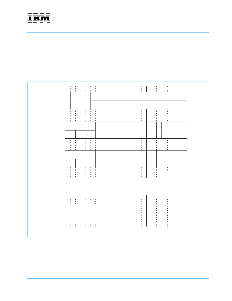
IBM PowerNP NP4GS3
Preliminary
Network Processor
np3_ds_sec05_Swi.fm.11
January 29, 2003
Switch Interface
Page 149 of 605
5.1.2 Frame Header
A frame header is a 10-byte field containing control information used by the target network processor and is
sent once per frame. A frame header can immediately follow the cell header, or with packing enabled, it can
also be placed at the start of the 2nd (D10), 3rd (D26), or 4th (D42) QW of the cell.
Figure 5-4 illustrates the format of a frame header; Table 5-2 provides the field definitions. Figure 5-5 illus-
trates the frame header fields in a 32-blade configuration.
Figure 5-4. Frame Header Format
1. See description of the correlator field in Frame Header Fields on page 150.
(1:0)
LID
Blade 64
r
r
r
r
r
r
Blade 16
Byte 0
Byte 1
Byte 2
FHE(31:8)
Byte 6
Byte 7
Byte 8
FHE(7:0)
Byte 9
Stake
(7:6)
MC
UC
MC
UC
MC
UC
(1:0)
LID
Stake(5:0)
Stake(5:0)
MID(16:0)
LID(20:2)
SP
SP
Byte 4
Byte 5
Byte 3
Correlator
1
with SB)
(overwritten
Correlator
1
with SB)
(overwritten
DSU
DSU
UC
nMC
FHF
FHF
FC Info

IBM PowerNP NP4GS3
Network Processor
Preliminary
Switch Interface
Page 150 of 605
np3_ds_sec05_Swi.fm.11
January 29, 2003
Figure 5-5. Frame Header Blade32 Format of Bytes 3-5
1. See description of the correlator field in Frame Header Fields on page 150.
Table 5-2. Frame Header Fields
Field Name
Description
Notes
UCnMC
Unicast - Multicast indicator. This 1-bit field indicates the format of the frame header.
`0'
Multicast format.
`1'
Unicast format.
1
FC Info
Flow Control Information (4-bit field). Indicates the type of connection used for this frame. Connection
type encoding is used by the NP4GS3's flow control mechanisms.
2
LID
Lookup Identifier (21 bit field). Used by the egress processing to locate the necessary information to
forward the frame to the appropriate target port with the correct QoS.
3
MID
Multicast Identifier (17 bit field). Used by the egress processing to locate the multicast tree informa-
tion which is used to forward the frame to the appropriate target ports with the correct QoS.
3
Stake
Available only for the multicast format of the frame header. This 8-bit field is used by egress process-
ing to locate the start of the Layer 3 header.
3
DSU
DSU indicator. Available only for the unicast format of the frame header. This 4-bit field indicates
which egress data stores are used by this frame when toggle mode is disabled (see 13.3 TB Mode
Register (TB_Mode) on page 473). Defined as follows (where "r" indicates a reserved bit that is trans-
mitted as `0' and is not modified or checked on receipt):
0rr0
Data store 0
0rr1
Data store 1
1rr0
Data store 0 and data store 1
1rr1
Data store 0 and data store 1
FHF
Frame Header Format. Software controlled field. This field, with the addition of the UC field, is used
by the hardware classifier in the EPC to determine the code entry point for the frame. The UC field
and the FHF form a 5-bit index into a configurable lookup table of code entry points used for egress
processing.
SP
Source port of the frame.
FHE
Frame Header Extension (32-bit field). Used by ingress processing to pass information to egress pro-
cessing. The contents of this field depend on the FHF value used by egress processing to interpret
the field. Information passed reduces the amount of frame parsing required by egress processing
when determining how to forward the frame.
r
Reserved field, transmitted as `0' . Should not be modified or checked by the switch fabric.
1. This field is used by egress reassembly logic in selection the reassembly control block. It is also used by the hardware classifier.
2. This field is passed through the ingress flow control before the frame is enqueued for transmission across the switch interface. It
can be used by software to allow the hardware to make further flow control decisions on egress by passing connection information
(type and DSCP).
3. This field is passed by the hardware but is defined and used by the software.
Blade 32
Byte 3
Byte 4
Byte 5
r
r
MC
UC
(1:0)
LID
Stake(5:0)
SP
Correlator
1
with SB)
(overwritten
DSU
FHF
r

IBM PowerNP NP4GS3
Preliminary
Network Processor
np3_ds_sec05_Swi.fm.11
January 29, 2003
Switch Interface
Page 151 of 605
Correlator
The size of this field depends on the blade operational mode. The SB information in the cell header is
copied into the byte occupied by the correlator (overlaying the correlator and some reserved bits)
when the frame header is written to the egress data store. This provides SB information for egress
processing.
16-blade Correlator values 0-63 are used for unicast traffic. Correlator values 0-31 are used for mul-
ticast traffic.
32-blade Correlator values 0-31 are used for unicast traffic. Correlator values 0-15 are used for mul-
ticast traffic.
64-blade Correlator values 0-15 are used for unicast traffic. Correlator values 0-7 are used for multi-
cast traffic.
Table 5-2. Frame Header Fields
Field Name
Description
Notes
1. This field is used by egress reassembly logic in selection the reassembly control block. It is also used by the hardware classifier.
2. This field is passed through the ingress flow control before the frame is enqueued for transmission across the switch interface. It
can be used by software to allow the hardware to make further flow control decisions on egress by passing connection information
(type and DSCP).
3. This field is passed by the hardware but is defined and used by the software.

IBM PowerNP NP4GS3
Network Processor
Preliminary
Switch Interface
Page 152 of 605
np3_ds_sec05_Swi.fm.11
January 29, 2003
5.2 Ingress Switch Cell Interface
The Ingress Switch Cell Interface (I-SCI) provides a continuous stream of transmit data to the DASL. After
power on or reset of the network processor, the I-SCI initialization process generates synchronization cells for
the DASL. When the DASL is synchronized, the I-SCI enters the operational state. When there are no data
cells to send, the I-SCI generates idle cells for transmission via the DASL. When there are data cells to send,
the I-SCI receives a logical cell from the I-SDM, translates the cell into the switch cell format, and transmits
the cell via the DASL. The I-SCI performs formatting on the cell headers to conform with the switch cell
format.
The I-SCI unit relies on an internal FIFO buffer (written by the I-SDM at the network processor core clock rate
and read at the Switch clock rate) performing the translation from logical cell format to switch cell format.
5.2.1 Idle Cell Format
When there is no data to send, idle cells are transmitted on the SWI. All bytes in an idle cell have the value
x`CC', except for the first three bytes in the master stream. Word 0, Word 1, and Word 2 of the master stream
contain H0, H1, and H2 respectively.
.
Table 5-3. Idle Cell Format Transmitted to the Switch Interface
Word #
Slave 1
(Byte 0)
Master
(Byte 1)
Slave 3
(Byte 2)
Slave 2
(Byte 3)
(bits 31:24)
(bits 23:16)
(bits 15:8)
(bits 7:0)
W0
x`CC'
H0
x`CC'
x`CC'
W1
x`CC'
H1 (x`CC')
x`CC'
x`CC'
W2
x`CC'
H2 (x`CC')
x`CC'
x`CC'
W3
x`CC'
x`CC'
x`CC'
x`CC'
W4
x`CC'
x`CC'
x`CC'
x`CC'
W5
x`CC'
x`CC'
x`CC'
x`CC'
W6
x`CC'
x`CC'
x`CC'
x`CC'
W7
x`CC'
x`CC'
x`CC'
x`CC'
W8
x`CC'
x`CC'
x`CC'
x`CC'
W9
x`CC'
x`CC'
x`CC'
x`CC'
W10
x`CC'
x`CC'
x`CC'
x`CC'
W11
x`CC'
x`CC'
x`CC'
x`CC'
W12
x`CC'
x`CC'
x`CC'
x`CC'
W13
x`CC'
x`CC'
x`CC'
x`CC'
W14
x`CC'
x`CC'
x`CC'
x`CC'
W15
CRC
CRC
CRC
CRC

IBM PowerNP NP4GS3
Preliminary
Network Processor
np3_ds_sec05_Swi.fm.11
January 29, 2003
Switch Interface
Page 153 of 605
5.2.1.1 CRC Bytes: Word 15
The cyclic redundancy check (CRC) bytes sent on each byte stream contain an 8-bit CRC checksum of the
polynomial X
8
+ X
4
+ X
3
+ X
2
+ 1. Each byte stream is independently calculated and the initial value loaded
into the CRC generator at the end of each idle cell (after Word 15) is x`D0'. The final CRC value is calculated
starting with the first byte following an idle cell up to (but not including) the byte sent as part of Word 15 in the
next idle cell. Figure 5-6 illustrates an example of the CRC calculation.
5.2.1.2 I-SCI Transmit Header for the Idle Cell
The idle cell header consists of three bytes, H0, H1, and H2, which are defined as follows:
� H0. Also referred to as the Qualifier byte, this 8-bit field indicates the type of cell being transmitted.
� H1 and H2. Set to x`CC'.
The following table provides the field definitions for H0:
Figure 5-6. CRC Calculation Example
Bit(s)
Definition
7
Reserved. Transmitted as `0'.
6
Switch cell header parity. This even parity bit covers the H0-H2 fields.
5:4
Data cell indicator.
`00'
Idle cell
`11'
Data cell
All other values are Reserved.
3:2
Reserved. Transmitted as `00'.
1:0
Reserved. This field should not be examined by the switch.
Idle cell
0
15
Data cell
0
15
Data cell
0
15
Idle cell
0
15
Bytes in
Stream
CRC calculated on these bytes
x`D0'
Initial
Value
Loaded
14
CRC Value
Stored in
Byte 15

IBM PowerNP NP4GS3
Network Processor
Preliminary
Switch Interface
Page 154 of 605
np3_ds_sec05_Swi.fm.11
January 29, 2003
5.2.2 Switch Data Cell Format - Ingress and Egress
Table 5-4 shows the format of data cells sent to and from the SWI via the DASL bus. Notice that the Packet
Routing Switch cell header bytes (H0, H1, and H2) are all contained in the master byte stream. Bytes desig-
nated CH0 through CH5 are the cell header bytes described in Figure 5-2. Cell Header Format on page 146.
Table 5-4. Switch Data Cell Format
Word #
Slave 1
DASL_Out_0
DASL_Out_1
Master
DASL_Out_2
DASL_Out_3
Slave 3
DASL_Out_4
DASL_Out_5
Slave 2
DASL_Out_6
DASL_Out_7
(bits 31:24)
(bits 23:16)
(bits 15:8)
(bits 7:0)
W0
CH5
CH0 (H0)
D9
D7
W1
D0
CH1 (H1)
D4
D2
W2
D1
CH2 (H2)
D5
D3
W3
CH4
CH3
D8
D6
W4
D25
D23
D21
D19
W5
D12
D10
D16
D14
W6
D13
D11
D17
D15
W7
D24
D22
D20
D18
W8
D41
D39
D37
D35
W9
D28
D26
D32
D30
W10
D29
D27
D33
D31
W11
D40
D38
D36
D34
W12
D57
D55
D53
D51
W13
D44
D42
D48
D46
W14
D45
D43
D49
D47
W15
D56
D54
D52
D50
1. DASL_Out_x (where x
{1, 3, 5, 7}) carry the even bits of the indicated bytes.
2. DASL_Out_x (where x
{0, 2, 4, 6}) carry the odd bits of the indicated bytes.
3. Dxx indicates the data byte in the cell from the SDM interface.
4. CHx indicates the cell header.

IBM PowerNP NP4GS3
Preliminary
Network Processor
np3_ds_sec05_Swi.fm.11
January 29, 2003
Switch Interface
Page 155 of 605
5.3 Data-Aligned Synchronous Link Interface
The data-aligned synchronous link (DASL) interface is a macro that facilitates high speed point-to-point inter-
chip communication. It provides the application designer the ability to relieve I/O constraints imposed by the
device package or card connector. The DASL interface performs multi-bit serialization and de-serialization to
reduce the I/O pin count. The interface is frequency-synchronous, which removes the need for asynchronous
interfaces that introduce additional interface latency. DASL links are intended to operate over a back-plane
without any additional components.
The DASL interface macro was developed to interface the core area of a CMOS ASIC to a high speed link.
The macro incorporates all the high-speed circuitry necessary to initialize and perform dynamic link timing
and data serialization/de-serialization without exposing the core designer to the specific implementation. The
core ASIC interface to DASL is a parallel interface. The DASL macro is scalable based on application needs.
The DASL macro was designed for high levels of integration. It uses reduced voltage differential transceivers
to reduce power consumption. The macro has been partitioned such that multiple sub-macros share a
common controller as well as a common phase-locked loop (PLL).
On the most basic level, the DASL macro is designed to provide a 4-to-1 serialization/de-serialization inter-
face. The NP4GS3 application utilizes a 32- to 8-bit (32-bit port) pin reduction. The shared DASL controller
(SDC) provides control for the DASL TX and DASL RX ports.

IBM PowerNP NP4GS3
Network Processor
Preliminary
Switch Interface
Page 156 of 605
np3_ds_sec05_Swi.fm.11
January 29, 2003
5.4 Egress Switch Cell Interface
The Egress Switch Cell Interface (E-SCI) receives cells from the switch fabric and passes data cells to the
Egress Switch Data Mover (E-SDM). The E-SCI discards idle cells received from the switch fabric, checks the
parity of the received cells, and discards cells with bad parity. The E-SCI strips out the target blade per-port
grant information from the switch cells and sends this grant information to the network processor Ingress units
for use in ingress data flow control. The E-SCI assists in egress data flow control by throttling the switch fabric
to prevent data overruns.
5.4.1 Master and Multicast Grant Reporting
The master and multicast grant (Master_Grant and MC_Grant) I/O signals report congestion in the attached
switch to the NP4GS3. When Master_Grant (see Section Table 2-1. Signal Pin Functions on page 40) indi-
cates congestion, the ingress scheduler is disabled from sending any traffic to the switch interface. When
Multicast_grant (see Section Table 2-1. Signal Pin Functions on page 40) indicates congestion, the Ingress
Scheduler is disabled from sending any multicast traffic to the switch interface.
5.4.2 Output Queue Grant Reporting
Most fields in the cell header must pass through the switch fabric unchanged (idle cells are not transmitted
through a switch fabric; they originate at the output port of the switch). The exception to this is the Target
Blade field (see Figure 5-2: Cell Header Format on page 146) which contains Output Queue Grant (OQG)
information used by the network processor's Ingress EDS when selecting data to be sent to the switch. A
target port is not selected if its corresponding Output Queue Grant information is set to `0'.
Further, Output Queue Grant information is sent for each of the three priorities supported by the network
processor. This is done using multiple cell transfers; starting with priority 0, reporting Output Queue Grant for
all supported target blades, then repeating this process for each priority level until a value of 2 is reached, and
starting over at priority 0 again.
For 16-blade operational mode, the sequence is:
1. Priority 0; OQG for blades 0:15 (H1 contains 0:7, H2 contains 8:15)
2. Priority 1; OQG for blades 0:15 (H1 contains 0:7, H2 contains 8:15)
3. Priority 2; OQG for blades 0:15 (H1 contains 0:7, H2 contains 8:15)
4. Start over at step 1.
The idle cell indicates the priority of the OQG it carries. This allows the network processor to synchronize with
the external switch.
For 32-blade operational mode, the sequence is:
1. Priority 0; OQG for blades 0:15 (H1 contains 0:7, H2 contains 8:15)
2. Priority 0; OQG for blades 16:31 (H1 contains 16:23, H2 contains 24:31)
3. Priority 1; OQG for blades 0:15 (H1 contains 0:7, H2 contains 8:15)
4. Priority 1; OQG for blades 16:31 (H1 contains 16:23, H2 contains 24:31)
5. Priority 2; OQG for blades 0:15 (H1 contains 0:7, H2 contains 8:15)
6. Priority 2; OQG for blades 16:31 (H1 contains 16:23, H2 contains 24:31)
7. Start over at step 1.

IBM PowerNP NP4GS3
Preliminary
Network Processor
np3_ds_sec05_Swi.fm.11
January 29, 2003
Switch Interface
Page 157 of 605
For 32-blade mode, this sequence is interrupted when an idle cell is sent. Table 5-7: Idle Cell Format
Received from the Switch Interface - 32-blade Mode on page 161 shows an idle cell that carries the OQG for
all blades. Status for each priority is given in increasing order; (P0 followed by P1 followed by P2). The
network processor restarts the sequence at step one with the arrival of the next data cell.
For 64-blade operational mode, the sequence is:
1. Priority 0; OQG for blades 0:15 (H1 contains 0:7, H2 contains 8:15)
2. Priority 0; OQG for blades 16:31 (H1 contains 16:23, H2 contains 24:31)
3. Priority 0; OQG for blades 32:47 (H1 contains 32:39, H2 contains 40:47)
4. Priority 0; OQG for blades 48:63 (H1 contains 48:55, H2 contains 56:63)
5. Priority 1; OQG for blades 0:15 (H1 contains 0:7, H2 contains 8:15)
6. Priority 1; OQG for blades 16:31 (H1 contains 16:23, H2 contains 24:31)
7. Priority 1; OQG for blades 32:47 (H1 contains 32:39, H2 contains 40:47)
8. Priority 1; OQG for blades 48:63 (H1 contains 48:55, H2 contains 56:63)
9. Priority 2; OQG for blades 0:15 (H1 contains 0:7, H2 contains 8:15)
10. Priority 2; OQG for blades 16:31 (H1 contains 16:23, H2 contains 24:31)
11. Priority 2; OQG for blades 32:47 (H1 contains 32:39, H2 contains 40:47)
12. Priority 2; OQG for blades 48:63 (H1 contains 48:55, H2 contains 56:63)
13. Start over at step 1.
For 64-blade mode, this sequence is interrupted when an idle cell is sent. Table 5-8 shows an idle cell that
carries the OQG for all blades. Status for each priority is given in increasing order; (P0 followed by P1
followed by P2). The network processor restarts the sequence at step one with the arrival of the next data
cell.
5.4.2.1 OQG Reporting in External Wrap Mode
When the NP4GS3 is configured for External Wrap mode (see bit 31 in Section 13.35.1 DASL Configuration
Register (DASL_Config) on page 547), OQG is not collected as described in Section 5.4.2. Instead, the
master grant I/O signals are used to collect this information.
In this mode of operation, only target blades 0 and 1 are valid addresses. OQG status for all other blade
addresses is always reported as zero to the Ingress Scheduler. Master_Grant_A is connected to
Send_Grant_A of the same NP4GS3, while Master_Grant _B of one NP4GS3 is connected to Send_Grant_B
of the other. Thus, the OQG status for TB0 is provided by Master_Grant_A on TB0 and from Master_Grant_B
on TB1. The OQG status for TB1 is provided by Master_Grant_B on TB0 and from Master_Grant_A on TB1.
Internally to both NP4GS3s, master grant is derived from the logical AND of both master grant I/O signals
(per priority).

IBM PowerNP NP4GS3
Network Processor
Preliminary
Switch Interface
Page 158 of 605
np3_ds_sec05_Swi.fm.11
January 29, 2003
Figure 5-8 on page 159 illustrates a single NP configuration. Note that in this configuration, the DASL A inter-
face is used. With Switch_BnA tied to 1, this makes this interface the "Alternate" (See 13.35.1.1 Dynamic
Switch Interface Selection on page 549). Since the NP must have the "Primary" active, even though it is not
used in this configuration, DASL_Bypass_Wrap must be enabled for the DASL B interface (13.35.2 DASL
Bypass and Wrap Register (DASL_Bypass_Wrap) on page 551) for proper operation.
My_TB is set to 0 for this blade, and both OQG status and internal Master Grant is provided by
Master_Grant_A.
Figure 5-7. External Wrap Mode (Two NP4GS3 interconnected)
TB1
TB0
DASL_In_B
DASL_Out_B
Master_Grant_
A
Send_Grant_B
DASL_In_A
Sen
d_Grant_A
DASL_Out_A
MC_Grant
_A
DASL A
Master_Grant
_A
DASL_In_A
Send_
Grant_A
D
A
SL_Out_A
MC
_Grant_A
DASL A
Master_Grant_B
DASL_In
_
B
DASL_Ou
t
_B
S
end
_G
ran
t
_
B
Master_Gran
t
_B
DASL B
DASL B
MC_
G
rant_B
MC_Grant_B
Switch_BnA
Switch_BnA
Tie 1
Tie 1
Tie 1
Tie 1
Note: In this configuration OQG status and Master Grant are not differentiated by priority.

IBM PowerNP NP4GS3
Preliminary
Network Processor
np3_ds_sec05_Swi.fm.11
January 29, 2003
Switch Interface
Page 159 of 605
5.4.3 Switch Fabric to Network Processor Egress Idle Cell
The Egress SWI Interface requires idle cells when there is no data. An idle cell requires:
� The last bytes on each stream contain a Trailer cyclic redundancy check (CRC).
� For the master stream, the header H0 as described in Table 5-5 on page 160.
� For the master stream, H1 - H2 contain the target blade grant priority information when in 16-blade mode.
� For the master stream, H1 - H2 contain x`CC' when in 32-blade mode.
� For the master stream, H1 - H2 contain x`CC' when in 64-blade mode.
� All other bytes contain x'CC' when in 16-blade mode or OQG (see Table 5-6 on page 160) when in
64-blade mode. For 32-blade mode see Table 5-7: Idle Cell Format Received from the Switch Interface -
32-blade Mode on page 161.
Figure 5-8. External Wrap Mode (single NP4GS3 configuration)
TB0
DASL_Out_B
M
a
ster_Grant_A
DASL_In_A
Send_Grant
_A
DASL_Out_A
MC_Grant
_A
DASL A
Master_Gran
t
_B
DASL_In_B
Se
nd_
Gra
n
t
_B
DASL B
MC
_Grant_B
Switch_BnA
Tie 1
Tie 1
Note: In this configuration OQG status and Master Grant are not differentiated by priority.
DASL B must be set up for internal wrap
The alternate port must be enabled:
DASL_Config(31) = 1 (External_Wrap_Mode)
DASL_Config(30:29) = '01' (GS_Mode)
MY_TB = 0
[DASL_ByPass_Wrap_En(31:30) = '10']
Tie 1
Tie 1

IBM PowerNP NP4GS3
Network Processor
Preliminary
Switch Interface
Page 160 of 605
np3_ds_sec05_Swi.fm.11
January 29, 2003
.
Table 5-5. Receive Cell Header Byte H0 for an Idle Cell
Bit(s)
Definition
7
Reserved. Transmitted as `0'.
6
Switch cell header parity. This even parity bit covers the H0-H2 fields.
5:4
Data cell indicator.
`00'
Idle cell
`11' Data
cell
All other values are Reserved.
3:2
Reserved. Transmitted as `00'.
1:0
Output Queue Grant priority. When in 16-blade mode, indicates the priority level of the Output Queue Grant information
carried in H1-H2. Otherwise the network processor ignores this field.
Table 5-6. Idle Cell Format Received from the Switch Interface - 16-blade Mode
Slave 1
Master 1
Slave 3
Slave 2
Byte 0
Byte 1
Byte 2
Byte 3
x`CC'
H0
x`CC'
x`CC'
x`CC'
H1 (OQG (0:7))
x`CC'
x`CC'
x`CC'
H2 (OQG (8:15))
x`CC'
x`CC'
x`CC'
x`CC'
x`CC'
x`CC'
x`CC'
x`CC'
x`CC'
x`CC'
x`CC'
x`CC'
x`CC'
x`CC'
x`CC'
x`CC'
x`CC'
x`CC'
x`CC'
x`CC'
x`CC'
x`CC'
x`CC'
x`CC'
x`CC'
x`CC'
x`CC'
x`CC'
x`CC'
x`CC'
x`CC'
x`CC'
x`CC'
x`CC'
x`CC'
x`CC'
x`CC'
x`CC'
x`CC'
x`CC'
x`CC'
x`CC'
x`CC'
x`CC'
x`CC'
x`CC'
CRC
CRC
CRC
CRC
IBM PowerNP NP4GS3
Preliminary
Network Processor
np3_ds_sec05_Swi.fm.11
January 29, 2003
Switch Interface
Page 161 of 605
Table 5-7. Idle Cell Format Received from the Switch Interface - 32-blade Mode
Slave 1
Master
Slave 3
Slave 2
Byte 0
Byte 1
Byte 2
Byte 3
x`CC'
H0
x`CC'
x`CC'
x`CC'
H1 (x`CC')
x`CC'
x`CC'
x`CC'
H2 (x`CC')
x`CC'
x`CC'
0 1
0
1
2
3
2
3
4
5
4
5
6
7
6
7
8
9
8
9
10 11 10 11 12 13 12 13 14 15 14 15
16 17 16 17 18 19 18 19 20 21 20 21 22 23 22 23 24 25 24 25 26 27 26 27 28 29 28 29 30 31 30 31
x`CC'
x`CC'
x`CC'
x`CC'
x`CC'
x`CC'
x`CC'
x`CC'
0 1
0
1
2
3
2
3
4
5
4
5
6
7
6
7
8
9
8
9
10 11 10 11 12 13 12 13 14 15 14 15
16 17 16 17 18 19 18 19 20 21 20 21 22 23 22 23 24 25 24 25 26 27 26 27 28 29 28 29 30 31 30 31
x`CC'
x`CC'
x`CC'
x`CC'
x`CC'
x`CC'
x`CC'
x`CC'
0 1
0
1
2
3
2
3
4
5
4
5
6
7
6
7
8
9
8
9
10 11 10 11 12 13 12 13 14 15 14 15
16 17 16 17 18 19 18 19 20 21 20 21 22 23 22 23 24 25 24 25 26 27 26 27 28 29 28 29 30 31 30 31
x`CC'
x`CC'
x`CC'
x`CC'
x`CC'
x`CC'
x`CC'
x`CC'
CRC
CRC
CRC
CRC
Table 5-8. Idle Cell Format Received from the Switch Interface - 64-blade Mode
Slave 1
Master
Slave 3
Slave 2
Byte 0
Byte 1
Byte 2
Byte 3
x`CC'
H0
x`CC'
x`CC'
x`CC'
H1 (x`CC')
x`CC'
x`CC'
x`CC'
H2 (x`CC')
x`CC'
x`CC'
0 1
0
1
2
3
2
3
4
5
4
5
6
7
6
7
8
9
8
9
10 11 10 11 12 13 12 13 14 15 14 15
16 17 16 17 18 19 18 19 20 21 20 21 22 23 22 23 24 25 24 25 26 27 26 27 28 29 28 29 30 31 30 31
32 33 32 33 34 35 34 35 36 37 36 37 38 39 38 39 40 41 40 41 42 43 42 43 44 45 44 45 46 47 46 47
48 49 48 49 50 51 50 51 52 53 52 53 54 55 54 55 56 57 56 57 58 59 58 59 60 61 60 61 62 63 62 63
CRC
CRC
CRC
CRC

IBM PowerNP NP4GS3
Network Processor
Preliminary
Switch Interface
Page 162 of 605
np3_ds_sec05_Swi.fm.11
January 29, 2003
5.4.4 Receive Header Formats for Sync Cells
Sync cells are a special type of idle cells. They are similar to the received idle cell for 16-blade mode (see
Table 5-6 on page 160) but H0, H1, and H2 are set to a value of x`CC'. All sync cells are discarded.
5.5 Egress Switch Data Mover
The Egress Switch Data Mover (E-SDM) is the logical interface between the switch cell data flow of the E-SCI
and the frame data flow of the Egress EDS. The E-SDM serves as a buffer for cells flowing from the E-SCI to
the Egress EDS. The E-SDM extracts control information, such as the frame correlator, which is passed to
the Egress EDS. The Egress EDS uses this control information, along with data from the E-SDM, to re-
assemble the cells into frames.
5.6 IBM Packet Routing Switch PRS28.4G Configuration Notes
When using the IBM Packet Routing Switch PRS28.4G, the following configuration settings are required.
1
� Mode Register
- Flow Control Check Enable must be inactive.
� Configuration Register 0
- Three threshold Enable must be set to `1'
- Enable one of the speed expansion modes. Internal when using a single PRS28.4G (provides 8
ports) or External when using two PRS28.4G (provides 16 ports).
- Priority Enable must be set to `10', which enables priority 0, 1 and 2.
- Grant Enable is set.
� Maximum recommended settings for Shared Memory Threshold Registers
- Shared Memory Threshold Register 0
� Threshold for Priority 0
`10101'
� Threshold for Priority 1
`10100'
- Shared Memory Threshold Register 1
� Threshold for Priority 2
`10011'
1. This list is not exhaustive, please contact your IBM field application engineer for assistance in using the IBM Packet Routing
Switch PRS28.4G with the NP4GS3.

IBM PowerNP NP4GS3
Preliminary
Network Processor
np3_ds_sec06_EEDS.fm.11
January 29, 2003
Egress Enqueuer / Dequeuer / Scheduler
Page 163 of 605
6. Egress Enqueuer / Dequeuer / Scheduler
The Egress Enqueuer / Dequeuer / Scheduler (Egress EDS) interfaces with the Physical MAC Multiplexer
(PMM), the Embedded Processor Complex (EPC), and the Egress Switch Interface (Egress SWI). It is
responsible for handling all the buffer, frame, and queue management for reassembly and transmission on
the egress side of the network processor.
The Egress EDS reassembles data that have been transported from a switch fabric through the data-aligned
synchronous link (DASL) interface to the Egress PMM. It reassembles frames sent from up to 64 network pro-
cessors (up to 3072 simultaneous reassemblies). Each switch cell received from the Egress SWI is examined
and stored in the appropriate Egress Data Store (Egress DS) for reassembly into its original frame. When the
frame is completely received from the SWI, the Egress EDS enqueues it to the EPC for processing.
Once the EPC processes the frame, it provides forwarding and quality of service (QoS) information to the
Egress EDS. The Egress EDS then invokes hardware configured flow control mechanisms and then
enqueues it to either the Scheduler, when enabled, or to a target port (TP) queue for transmission to the
Egress PMM (which, in turn, sends the data to physical layer devices).
The Egress EDS supports the following functions, as illustrated in Figure 6-1 on page 164:
� External Egress Data Store
� Automatic allocation of buffer and frame control blocks for each frame
� EPC queues (GFQ, GTQ, GR0, GR1, GB0, GB1, and GPQ)
� Target port queues with two priorities
� Buffer thresholds and flow control actions
� Bandwidth and best effort scheduling
� Reading and writing of frame data stored in Egress Data Store
� Up to 512 K buffer twins depending on memory configuration
� Up to 512 K of frame control blocks (FCBs) depending on memory configuration
� Unicast and multicast frames
� Cell packing
� 40 external ports plus wrap port interface to the PMM
� Discard function
� Hardware initialization of internal and external data structures
IBM PowerNP NP4GS3
Network Processor
Preliminary
Egress Enqueuer / Dequeuer / Scheduler
Page 164 of 605
np3_ds_sec06_EEDS.fm.11
January 29, 2003
6.1 Functional Blocks
Figure 6-1 illustrates the functional blocks of the Egress EDS. The list following the figure explains each func-
tional block.
Figure 6-1. Egress EDS Functional Blocks
E
Data Store Interface
Writes the external Egress DS during frame reassembly and reads them during
frame transmission. Also gives the EPC access to the Egress DS. The Data Store
Interface supports two external data stores: DS0 and DS1.
DPQ
Discard Port Queue. Releases twin buffers back to the free queue stack. The pico-
code uses this queue to discard frames where header twins have been allocated.
E-GDQ
Discard Queue Stack. Holds frames that need to be discarded. The hardware uses
this queue to discard frames when the egress DS is congested or to re-walk a
frame marked for discard for a half-duplex port. The picocode uses this queue to
discard frames that do not have header twins allocated.
Egress PCB
Egress Port Control Block. Contains the necessary information to send a frame to
the Egress PMM for transmission. The Egress EDS uses this information to walk
the twin buffer chain and send the data to the Egress PMM's output port. There is a
PCB entry for each target port, plus one for Discard and one for Wrap. Each entry
holds information for two frames: the current frame being sent to the PMM port and
the next frame to be sent.
Data
Store
Interface
Egress PCB
RCB
Release
Logic
MCC Tables
Fl
o
w
Co
ntrol
WRAPQ
DP
Q
T
P
39Q_P1
T
P
0Q_PO
GB1
GB0
GR1
GR0
GT
Q
GF
Q
FQ
S
Egress
PMM
Egress
EPC
E-GDQ
SWI
DS
GPQ
FCBF
Q
Sched
uler

IBM PowerNP NP4GS3
Preliminary
Network Processor
np3_ds_sec06_EEDS.fm.11
January 29, 2003
Egress Enqueuer / Dequeuer / Scheduler
Page 165 of 605
FCBFQ
Frame Control Block Free Queue. Lists free Egress FCBs. FCBs store all the infor-
mation needed to describe the frame on the egress side, such as starting buffer,
length, MCC address, frame alteration, and so on. The Egress EDS obtains an
FCB from the free queue when the EPC enqueues the frame to either a flow QCB
(see Flow Queues on page 180) or a TP after EPC processing and flow control
actions are complete.
FQS
Free Queue Stack. Holds a list of free egress twin buffers which are used by the
Egress EDS during frame reassembly and by the EPC during frame alteration. The
twin buffers store the frame data or frame alteration header twins and also contain
the link pointer to the next buffer in the chain. The FQS obtains a new free twin
buffer any time the Egress EDS needs one and returns free twin buffers after
frames are discarded or transmitted.
GB0, GB1
Low Priority Data Queues. GB0 is for frames stored in Egress DS0. GB1 is for
frames stored in Egress DS1.
GFQ
Guided Frame Queue. Queue that contains guided frames for delivery for the
Egress side of the network processor to the Guided Frame Handler.
GPQ
PowerPC queue. Queue that contains frames re-enqueued for delivery to the
General PowerPC Handler (GPH) thread for processing.
GR0, GR1
High Priority Data Queues. GR0 is for frames stored in Egress DS0. GR1 is for
frames stored in Egress DS1.
GTQ
General Table Queue. Queue that contains guided frames re-enqueued by pico-
code for delivery to the General Table Handler (GTH) thread.
MCC Table
Multicast Count Table. Each entry stores the number of multicast frames associ-
ated with a particular set of twin buffers. If a frame is to be multicast to more than
one target port, the EPC enqueues the frame to each target port, causing an entry
in the MCC Table to be incremented. As each target port finishes its copy of the
frame, the MCC Table entry is decremented. When all ports have sent their copies
of the frame, the associated twin buffers are released.
RCB
Reassembly Control Block. Used by the Egress EDS to reassemble the cells
received from the switch fabric into their original frames. Contains pointers to the
Egress DS to specify where the contents of the current cell should be stored. Helps
the Egress EDS keep track of the frame length and which EPC queue to use.
Release Logic
Releases twin buffers after the PMM has finished with the contents of the buffer.
The Release Logic checks the MCC Table to determine if the buffer can be
released or is still needed for some other copy of a multicast frame.
TP0Q - TP39Q
Target Port Queues. Hold linked lists of frames destined for a TP. Two queues are
associated with each of the 40 possible TPs. These queues are prioritized from
high (P0) to low (P1) using a strict priority service scheme (all higher priority
queues within a target port set must be empty before starting a lower priority
queue).

IBM PowerNP NP4GS3
Network Processor
Preliminary
Egress Enqueuer / Dequeuer / Scheduler
Page 166 of 605
np3_ds_sec06_EEDS.fm.11
January 29, 2003
6.2 Operation
The Egress EDS receives switch cells from the Egress Switch Interface (SWI) along with information that has
been preprocessed by the Egress Switch Data Mover (SDM) such as the Reassembly Correlator, source
blade, multicast indication, priority, and target data store (DS). In order to optimize the data transfer to an
Egress DS, the Egress EDS uses the target DS's information to determine which Egress SDM to service. The
two Egress DSs, DS0 and DS1, use alternating write windows, meaning the Egress EDS can write one cell to
one data store each "cell window time" (the time needed to store an entire switch cell (64 bytes) in external
DRAM). Cell window time is configured using the DRAM Parameter Register's 11/10 field.
After the appropriate Egress SDM has been selected, the Egress EDS reads the cell data out of the SDM and
uses the Reassembly Correlator, source blade, multicast indication, and priority information to index into the
Reassembly Control Block (RCB). The RCB contains all the information needed to reassemble the frame,
including the buffer address to use in the Egress DS. The cell data is stored in the buffer and the RCB is
updated to prepare for the next cell associated with the same frame. The Egress EDS manages 3072 RCB
entries, and each entry contains information such as start-of-frame indicator, data store buffer address,
current reassembled frame length, and queue type. Cells from several source blades are interleaved coming
from the SWI, and the Egress EDS uses the RCB information to rebuild each frame.
The RCB information is also used to check for missing cells. The length of the currently assembled frame is
compared to the sequence number in the end pointer field of the cell header of each incoming cell except the
final cell of a frame. In cells containing frame-ends, the end pointer field contains the actual end pointer value.
As a result, the hardware cannot detect missing cells just prior to the last cell of a frame.
The Egress EDS uses a free buffer from the head of the free queue stack (FQS) as needed to store frame
data in the Egress DS. The Egress EDS stores the cell data in the appropriate buffer and also stores the
buffer chaining information over the cell header data. When a packed cell arrives, the Egress EDS stores
each frame's information in two separate twin buffers. The first portion of the packed cell contains the end of
a frame. This data is stored in the appropriate twin buffer as pointed to by the RCB. The remaining portion of
the packed cell is the beginning of another frame and this data is stored in a second twin buffer as indicated
by the second frame's RCB entry. Figure 6-2 illustrates the cell buffers and storage in an Egress DS.
WRAPQ
Wrap Queue. Two wrap queues, one for guided frames and one for data frames,
send frames from the egress side to the ingress side of the network processor.
These queues allow the network processor to respond to a guided frame sent from
a remote control point function (CPF). The guided frame is received from the switch
fabric on the egress side and is wrapped to the ingress side to allow a response to
be sent to the CPF across the switch fabric. A data frame may be wrapped when
processing on a remote CPF is required.

IBM PowerNP NP4GS3
Preliminary
Network Processor
np3_ds_sec06_EEDS.fm.11
January 29, 2003
Egress Enqueuer / Dequeuer / Scheduler
Page 167 of 605
When the entire frame is reassembled, the Egress EDS enqueues it to one of several EPC queues. If the
reassembled frame is a guided frame, the Egress EDS uses the GFQ. High priority frames are placed in
either the GR0 or the GR1. Low priority frames are placed in either the GB0 or the GB1. The EPC services
these queues and requests a programmable amount of read data from the various frames in order to process
them (see Table 7-84: Port Configuration Memory Content on page 287). The Egress EDS reads the data
from the Egress Data Store and passes it back to the EPC. Additional reads or writes can occur while the
EPC is processing the frame. The Egress EDS performs all necessary reads or writes to the Egress Data
Store as requested by the EPC.
When the frame has been processed, the EPC enqueues the frame to the Egress EDS. If the frame's destina-
tion is the General Table Handler (GTH), the Egress EDS enqueues the frame to the GTQ. If the frame is to
Figure 6-2. Cell Formats and Storage in the Egress DS
CH
1
(0:5)
FH
1
(0:9)
FD
1
(00:15)
FD
1
(16:31)
FD
1
(32:47)
CH
1
(0:5)
FH
1
(0:9)
FD
1
(00:15)
FD
1
(16:31)
FD
1
(32:47)
CH
1
(0:5)
FD
1
(48:57)
FD
1
(58:73)
FD
1
(74:89)
FD
1
(90:105)
LP
1
(0:5)
FD
1
(48:57)
FD
1
(58:73)
FD
1
(74:89)
FD
1
(90:105)
FQS
FQS
CH
2
(0:5)
FD
2
(22:31)
FD
2
(32:47)
FD
2
(48:63)
FD
2
(64:79)
LP
2
(0:5)
FD
2
(22:31)
FD
2
(32:47)
FD
2
(48:63)
FD
2
(64:79)
CH
1
(0:5)
FD
1
(106:115)
FD
1
(116:120)
FH
2
(0:9)
FD
2
(00:05)
FD
2
(06:21)
CH
1
(0:5)
FD
1
(106:115)
FD
1
(116:120)
na (0:10)
FH
2
(0:9)
FD
2
(00:05)
FD
2
(06:21)
128-byte Linked Twin Buffers
for Frame 1
128-byte Linked Twin Buffers
for Frame 2
Non-Packed Start
of Frame Cell
Non-Packed
Continuation Cell
Packed End of
Frame Cell
Non-Packed
Continuation Cell
CH = Cell Header
FH = Frame Header
FD = Frame Data
LP = Link Pointer
na = unused bytes
Data Buffer
Data Buffer
Twin Buffer

IBM PowerNP NP4GS3
Network Processor
Preliminary
Egress Enqueuer / Dequeuer / Scheduler
Page 168 of 605
np3_ds_sec06_EEDS.fm.11
January 29, 2003
be discarded, it is placed in the DPQ. If the frame needs to be wrapped to the Ingress side, it is placed in the
Wrap Queue (if the scheduler is disabled) or into a QCB configured for wrap traffic. All other frames are
subject to flow control actions. If flow control does not discard the frame, the frame is placed into the Sched-
uler, if enabled, or placed directly into a target port queue. Each target port supports two priorities and there-
fore has two queues. The EPC indicates which target port and which priority should be used for each frame
enqueued. The two queues per port use a strict priority scheme, which means that all high priority traffic must
be transmitted before any lower priority traffic will be sent.
Frames destined for the Scheduler, target ports, or wrap ports have a frame control block (FCB) assigned by
the Egress EDS. The FCB holds all the information needed to transmit the frame including starting buffer
address, frame length, and frame alteration information, as illustrated in Figure 6-3. If the EPC needs to
forward more than one copy of the frame to different target ports, an entry in the MCC Table is used to indi-
cate the total number of copies to send. The EPC enqueues the frame to different target ports or different flow
QCBs and each enqueue creates a new FCB with (possibly) its own unique frame alteration.
Figure 6-3. TPQ, FCB, and Egress Frame Example
Target Port Queues
Frame Control
Blocks
Target Port 5
Target Port 9
Multicast Frame
Last Frame in
Target Port Queue 5
First Frame in
Target Port Queue 9
Unicast Frame
Last Frame in
Target Port Queue 9
Unicast Frame
First Frame in
Target Port Queue 5
H C = 2 T
H C = 2 T
FBA FL = y
FBA FL = y
FBA FL = x
FBA FL = z
H = Head
T = Tail
C = Queue Count
FBA = First Buffer Address
FL = Frame Length
Buf = Buffer
LP = Link Pointer
Frame Length
= x bytes
Frame Length
= y bytes
Frame Length
= z bytes
Buf 32
Buf 12
Buf 3
Buf 9
Buf 7
Buf 23
Buf 15
Buf 39
Buf 99
LP = 9
LP = 15
LP = 23
LP = 39
LP = 99
LP = 7

IBM PowerNP NP4GS3
Preliminary
Network Processor
np3_ds_sec06_EEDS.fm.11
January 29, 2003
Egress Enqueuer / Dequeuer / Scheduler
Page 169 of 605
When a frame reaches the head of a target port queue, it is placed in the Egress Port Control Block (PCB)
entry for that port and the FCB for that frame is placed on the FCB Free Queue. The Egress EDS uses the
PCB to manage frames being sent to the PMM for transmission. The PCB stores information needed to
retrieve frame data, such as current buffer address and frame length, from the Egress DS. The PCB allows
up to 40 frames to be retrieved simultaneously from the Egress DS. The PCB also supports the Wrap Port
and the Discard Port Queue. As data is retrieved from the Egress DS and passed to the PMM, the PCB moni-
tors transfers and stores buffer link pointers that enable the PCB to walk the buffer chain for the frame. When
the entire buffer chain has been traversed, the PCB entry is updated with the next frame for that target port.
As the PMM uses the data from each buffer, it passes the buffer pointer back to the Release Logic in the
Egress EDS. The Release Logic examines the MCC Table entry to determine if the buffer should be returned
to the FQS. (Half-Duplex ports will not have their twin buffers released until the entire frame has been trans-
mitted, in order to to support the recovery actions that are necessary when a collision occurs on the Ethernet
media.) If the MCC entry indicates that no other copies of this frame are needed, the buffer pointer is stored in
the FQS. However, if the MCC entry indicates that other copies of this frame are still being used, the Egress
EDS decrements the MCC entry, but does no further action with this buffer pointer.
The DPQ contains frames that have been enqueued for discard by the EPC and by the Release Logic. The
hardware uses the DPQ to discard the last copy of frames transmitted on half duplex ports. The DPQ is
dequeued into the PCB's discard entry, where the frame data is read from the DS to obtain buffer chaining
information necessary to locate all twin buffers of the frame and to release these twin buffers back to the free
pool (FQS).
6.3 Egress Flow Control
Flow control (whether to forward or discard frames) in the network processor is provided by hardware assist
mechanisms and picocode that implements a selected flow control algorithm. In general, flow control algo-
rithms require information about the congestion state of the data flow, including the rate at which packets
arrive, the current status of the data store, the current status of target blades, and so on. A transmit proba-
bility for various flows is an output of these algorithms.
The network processor implements flow control in two ways:
� Flow control is invoked when the frame is enqueued to either a target port queue or a flow queue control
block (QCB). The hardware assist mechanisms use the transmit probability along with tail drop conges-
tion indicators to determine if a forwarding or discard action should be taken during frame enqueue oper-
ation. The flow control hardware uses the picocode's entries in the egress transmit probability memory to
determine what flow control actions are required.
� Flow control is invoked when frame data enters the network processor. When the Egress DS is suffi-
ciently congested, these flow control actions discard all frames. The threshold that controls the invocation
of these actions is FQ_ES_Threshold_0 (see Table 6-1: Flow Control Hardware Facilities on page 170 for
more information).
6.3.1 Flow Control Hardware Facilities
The hardware facilities listed in Table 6-1 are provided for the picocode's use when implementing a flow
control algorithm. The picocode uses the information from these facilities to create entries in the Egress
transmit probability memory. The flow control hardware uses these entries when determining what flow
control actions are required.

IBM PowerNP NP4GS3
Network Processor
Preliminary
Egress Enqueuer / Dequeuer / Scheduler
Page 170 of 605
np3_ds_sec06_EEDS.fm.11
January 29, 2003
Table 6-1. Flow Control Hardware Facilities
(Page 1 of 2)
Name Definition
Access
Free Queue Count
Instantaneous count of the number of free twins available in the Egress Data Store.
CAB
FQ_ES_Threshold_0
Threshold for Free Queue Count. When the Free Queue Count < FQ_ES_Threshold_0, no
further twins are allocated for incoming data. User packets that have started reassembly are
discarded when they receive data when this threshold is violated. Guided traffic is not dis-
carded. The number of packets discarded is counted in the Reassembly Discard Counter.
When this threshold is violated, an interrupt (Class 0, bit 4) is signaled.
CAB
FQ_ES_Threshold_1
Threshold for Free Queue Count. When the Free Queue Count < FQ_ES_Threshold_1, an
interrupt (Class 0, bit 5) is signaled.
CAB
FQ_ES_Threshold_2
Threshold for Free Queue Count. When the Free Queue Count < FQ_ES_Threshold_2, an
interrupt (Class 0, bit 6) is signaled, and if enabled by DMU configuration, the Ethernet MAC
preamble is reduced to 6 bytes.
CAB
Arrival Rate Counter
The arrival rate of data into the Egress Data Store. This counter increments each time there
is a dequeue from the Twin Free Queue. When read by picocode via the CAB, this counter is
set to 0 (Read with Reset).
CAB
FQ Count EWMA
The calculated EWMA of the Free Queue Count.
CAB
P0 Twin Count
The number of Twins in priority 0 packets that have been enqueued to flow queues, but have
not been dequeued from target port queues.
CAB
P1 Twin Count
The number of twins in priority 1 packets that have been enqueued to flow queues, but have
not been dequeued from target port queues.
CAB
P0 Twin Count Threshold
Threshold for P0 Twin Count. It is used when determining flow control actions against Priority
0 traffic.
When P0 Twin Count > P0 Twin Count Threshold, the flow control hardware will discard the
frame.
CAB
P1 Twin Count Threshold
Threshold for P1 Twin Count. It is used when determining flow control actions against Priority
1 traffic.
When P1 Twin Count > P1 Twin Count Threshold, the flow control hardware will discard the
frame.
CAB
Egress P0 Twin Count EWMA
The calculated EWMA based on the count of the number of twins allocated to P0 traffic dur-
ing the sample period. Hardware maintains a count of the number of twins allocated to P0
traffic at enqueue.
CAB
Egress P1Twin Count EWMA
The calculated EWMA based on the count of the number of twins allocated to P1 traffic dur-
ing the sample period. Hardware maintains a count of the number of twins allocated to P1
traffic at enqueue.
CAB
Egress P0 Twin Count EWMA
Threshold
The congestion status of the Egress Data Store in each target blade. It is the result of a com-
parison between this configured threshold and the EWMA of the offered rate of priority 0 traf-
fic (P0 Twin Count EWMA > P0 Twin Count EWMA threshold). This information is
transmitted to remote blades via the res_data I/O and is collected in the Remote TB Status 0
register in the ingress flow control hardware.
CAB

IBM PowerNP NP4GS3
Preliminary
Network Processor
np3_ds_sec06_EEDS.fm.11
January 29, 2003
Egress Enqueuer / Dequeuer / Scheduler
Page 171 of 605
6.3.2 Remote Egress Status Bus
The Remote Egress Status (RES) Bus communicates the congestion state of the Egress Data Stores of all
nets in a system to the Ingress Flow Control of every NP4GS3 in that system. The ingress portion of each
NP4GS3 can then preemptively discard frames destined for a congested NP4GS3 without consuming addi-
tional bandwidth through the switch.
6.3.2.1 Bus Sequence and Timing
The RES Bus consists of two bidirectional signals:
1. RES_Data. This signal is time-division multiplexed between all the NP4GS3s in a system. Only one
NP4GS3 at a time drives this signal. Each NP4GS3 drives two priorities of congestion status sequentially.
All of the NP4GS3s in a system sample this data and store it for use by the Ingress Flow Control to make
discard decisions.
2. RES_Sync. This signal is received by all NP4GS3s in a system. Each NP4GS3 detects a transition of this
signal to derive its time slot to drive Egress data store congestion information. In NP4GS3B (R2.0), the
falling transition is used. In NP4GS3C (R3.x), either the falling or rising edge can be used and is config-
urable using the Remote Egress Status Bus Configuration Enables register's RES_Sync_Polarity field
(see 13.15.6 Remote Egress Status Bus Configuration Enables (RES_Data_Cnf) on page 515). This sig-
nal is periodic and repeats to allow the NP4GS3s to resynchronize after 16, 32, or 64 time slots have
passed, depending on the value of the TB Mode register. In a system, one NP4GS3 can be configured to
drive this signal to the other NP4GS3s. Alternatively, an external device can provide the stimulus for this
signal.
Figure 6-4 on page 172 shows a timing diagram of the operation of the RES Bus.
Egress P1 Twin Count EWMA
Threshold
The congestion status of the Egress Data Store in each target blade. It is the result of a com-
parison between this configured threshold and the EWMA of the offered rate of priority 0 traf-
fic. (P1 Twin Count EWMA > P1 Twin Count EWMA threshold). This information is
transmitted to remote blades via the res_data I/O and is collected in the Remote TB Status 1
register in the ingress flow control hardware.
CAB
Target Port TH_PQ+FQ
Target Port port queue plus egress scheduler (flow QCB) threshold. The target port queues
maintain a count of the number of twins allocated to the target port. The count is incremented
on enqueue (after flow control transmit action is taken) and decremented on dequeue from
the target port. Thresholds for each priority can be configured for for all ports (0:39). When
the number of twins assigned to a target port queue exceeds the threshold, its threshold
exceed status is set to 1. The status is used to index into the transmit probability memory for
packets going to the target port.
CAB
QCB Threshold
Flow queue threshold. When the number of twins assigned to this flow queue exceeds this
threshold, the threshold exceed status is set to 1. The status is used to index into the trans-
mit probability memory.
CAB
Table 6-1. Flow Control Hardware Facilities
(Page 2 of 2)
Name Definition
Access
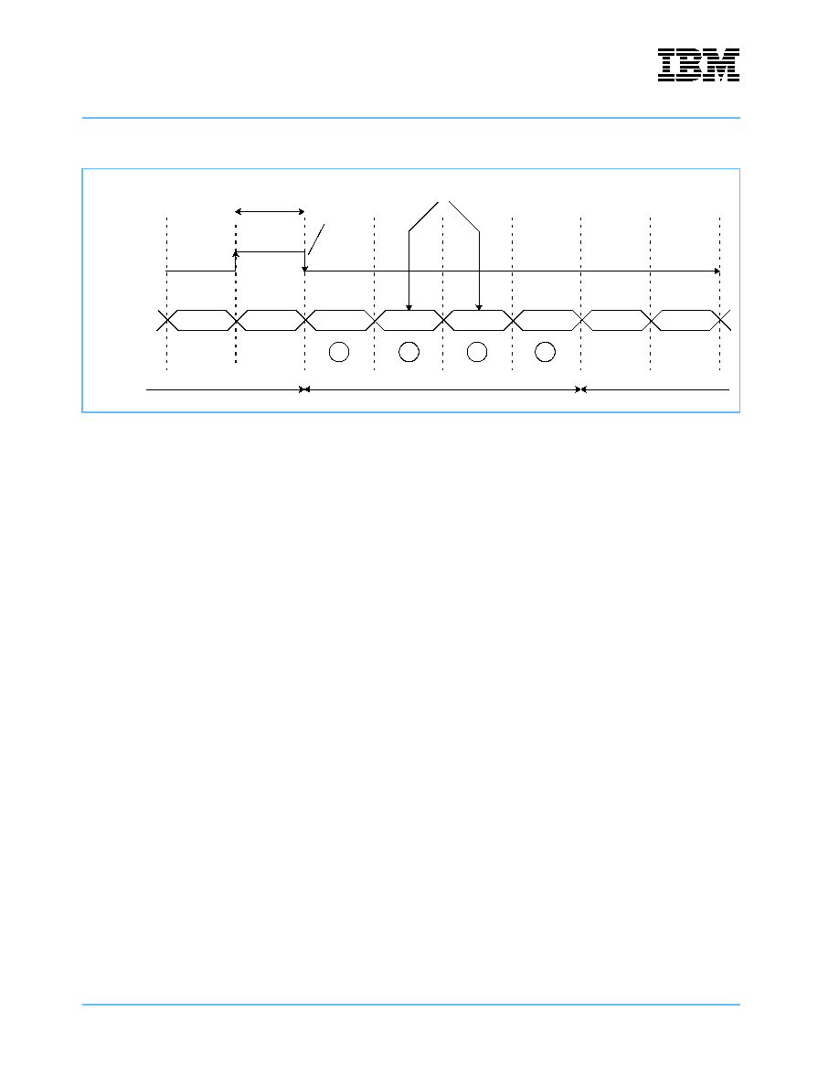
IBM PowerNP NP4GS3
Network Processor
Preliminary
Egress Enqueuer / Dequeuer / Scheduler
Page 172 of 605
np3_ds_sec06_EEDS.fm.11
January 29, 2003
Figure 6-4 illustrates the timings used for Res_Sync and Res_Data. Res_Sync is shown positive active (the
falling transition is used to determine where the Res_data bus sequence starts).
This is the operation for NP4GS3B (R2.0) and is configured in NP4GS3C (R3.x) using the reset value of
Remote Egress Status Bus Configuration Enables offset 1.
The RES Bus operates on the same clock frequency as the internal DASL clock. This clock period can range
from 8 ns to 10 ns. However, the RES Bus clock is not necessarily in phase with the DASL clock. In addition,
each NP4GS3 is not necessarily in phase with other NP4GS3s in the same system. The RES_Sync signal is
used for synchronizing all the NP4GS3s' usage of the RES data bus.
The RES Bus is time-division multiplexed between every NP4GS3 in the system. Each NP4GS3 moves its
congestion information onto the RES Bus in the order of its My_TB register (that is, the NP4GS3 with a
My_TB setting of 0 drives immediately after the active transition of RES_Sync, followed by the NP4GS3 with
a My_TB setting of 1, and so on).
Within each NP4GS3 time slot, the NP4GS3 puts four values on the RES_Data signal. Each value is held for
eight DASL clock cycles. Therefore, each NP4GS3 time slot is 32 DASL clock cycles. The protocol for
sending the congestion information is as follows:
1. High-Z. The NP4GS3 keeps its RES_Data line in high impedance for eight DASL clock cycles. This
allows the bus to turn around from one NP4GS3 to another.
2. P0. The NP4GS3 drives its Priority 0 (P0) Egress Data Store congestion information for eight DASL clock
cycles. Congestion is indicated when the Egress P0 Twin Count EWMA register value is greater than the
Egress P0 Twin Count EWMA Threshold register value. An NP4GS3B (R2.0) drives the Res_Data bus
high when congestion is indicated and low when it is not indicated. An NP4GS3C (R3.x) can be config-
ured via the Remote Egress Status Bus Configuration Enables offset 1 register (see 13.15.6 Remote
Egress Status Bus Configuration Enables (RES_Data_Cnf) on page 515) to operate in the same manner
as the NP4GS3B (R2.0) (using the reset state), or can drive the Res_Data bus low when congestion is
indicated and high when it is not.
3. P1. The NP4GS3 drives its Priority 1 (P1) Egress Data Store congestion information for eight DASL clock
cycles. Congestion is indicated when the Egress P1 Twin Count EWMA register value is greater than the
Egress P1 Twin Count EWMA Threshold register value. An NP4GS3B (R2.0) drives the Res_Data bus
high when congestion is indicated and low when it is not indicated. An NP4GS3C (R3.x) can be config-
Figure 6-4. RES Bus Timing
RES_Sync
RES_Data
P1
Reserved
Z
P0
P1
Reserved
Z
P0
1
2
3
4
NP 0
NP 1
NP N
8 DASL
cycles
Sampling
Points
Active
Transition

IBM PowerNP NP4GS3
Preliminary
Network Processor
np3_ds_sec06_EEDS.fm.11
January 29, 2003
Egress Enqueuer / Dequeuer / Scheduler
Page 173 of 605
ured via the Remote Egress Status Bus Configuration Enables offset 1 register (see 13.15.6 Remote
Egress Status Bus Configuration Enables (RES_Data_Cnf) on page 515) to operate in the same manner
as the NP4GS3B (R2.0) (using the reset state of the register), or can drive the Res_Data bus low when
congestion is indicated and high when it is not.
4. Reserved. The NP4GS3 drives a low value for eight DASL clock cycles. This is reserved for future use.
The Ingress Flow Control samples RES_Data during the midpoint of its eight DASL clock cycles in the
NP4GS3B (R2.0), and is configurable in the NP4GS3C (R3.x) (see 13.15.6 Remote Egress Status Bus
Configuration Enables (RES_Data_Cnf) on page 515).
The RES_Sync signal is driven to its active state during the Reserved cycle of the last NP4GS3's time slot. In
NP4GS3B (R2.0) the active state is high. In NP4GS3C (R3.x), the active state is configurable using the
Remote Egress Status Bus Configuration Enables register's RES_Sync_Polarity field (see 13.15.6 Remote
Egress Status Bus Configuration Enables (RES_Data_Cnf) on page 515). The RES_Sync signal therefore
has a period equal to 32 DASL clock periods multiplied by the number of NP4GS3s supported in this system.
The number of NP4GS3s can be either 16, 32, or 64 depending on the value of the TB Mode register.
6.3.2.2 Configuration
The RES Bus is activated by enabling the ingress and egress functions of the internal RES data logic via the
RES_Bus_Configuration_En register. Three bits in this register enable different functions:
� The I_RES_Data_En bit enables the ingress logic to capture the RES_Data.
� The E_RES_Data_En bit enables the egress logic to send its status on RES_Data.
� The E_RES_Sync_En bit enables one of the NP4GS3s to drive RES_Sync.
In a standard blade configuration (one NP4GS3 on each blade in a system), the RES Bus supports up to two
NP4GS3s without using external transceivers. The RES_Sync and RES_Data lines are wired together, and
one of the NP4GS3s is configured to drive RES_Sync. If, however, more than two NP4GS3s are to coexist in
a system and external transceivers are NOT used, a hub-based configuration must be implemented. Figure
6-5 shows such a configuration.

IBM PowerNP NP4GS3
Network Processor
Preliminary
Egress Enqueuer / Dequeuer / Scheduler
Page 174 of 605
np3_ds_sec06_EEDS.fm.11
January 29, 2003
The hub is necessary to drive the required signal strength to all of the NP4GS3s in a system when not using
external transceivers, and is connected point-to-point to each NP4GS3. The hub collects all RES_Data infor-
mation from the Egress logic of every NP4GS3 and then distributes it based on the timing diagram in Figure
6-5 to every NP4GS3's Ingress logic. The RES_Sync signal should be generated by the hub.
In either the Hub-based configuration or the shared bus configuration (with or with out the external drivers)
the following is recommended:
1. Board traces for all res_data bus connections to all NPs must be the same length (sync and data must
also be the same length).
2. By following rule 1 above, some variation can be handled with the sample offset controls provided in
Remote Egress Status Bus Configuration Enables (RES_Data_Cnf) Offset 2 (page 515).
3. For configurations greater than two NP4GS3s, a separate source for the sync is recommended since the
sync source gets the sync immediately while the other NP4GS3s will be offset by any cable delay. This
may make finding a sample point more difficult when comparing the use of an external source to the use
of an NP source for the sync pulse.
The NP4GS3C (R3.x) provides additional configuration support for implementing a solution using external
transceivers. The RES_Data_Active_Drv_En and RES_Sync_Active_Drv_En bits of the Remote Egress
Status Bus Configuration Enables (RES_Data_Cnf) Offset 1 (page 515) must be set high when external
transceivers are used. This enables all of the NP4GS3s in a system to drive separate enable lines to activate
external transceivers. Figure 6-6 on page 175 shows an example of external transceiver usage with the RES
Bus.
Figure 6-5. Hub-based RES Bus configuration to support more than two NP4GS3s
RES_Sync
RES_Data
NP 0
NP 1
NP N
RES Bus Hub
RES_Sync
RES_Sync
RES_Data
RES_Data
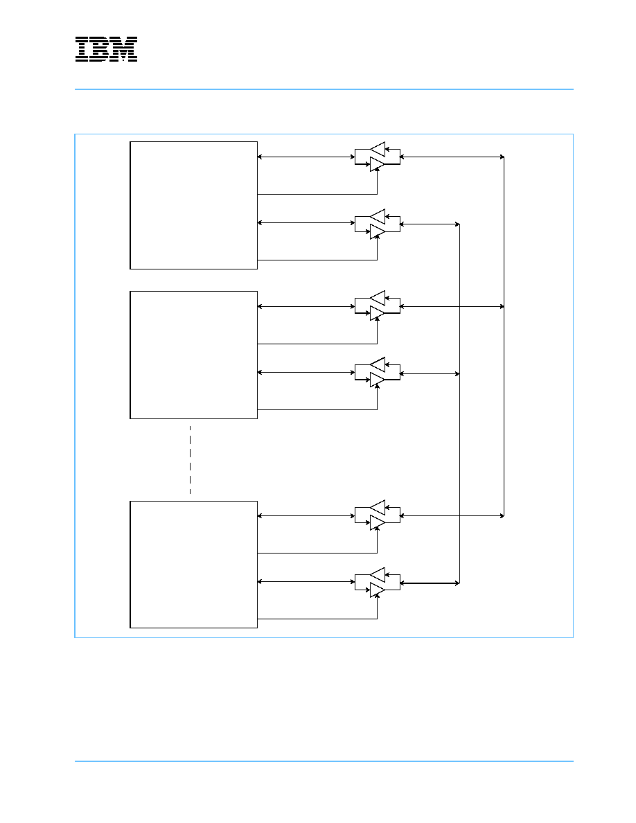
IBM PowerNP NP4GS3
Preliminary
Network Processor
np3_ds_sec06_EEDS.fm.11
January 29, 2003
Egress Enqueuer / Dequeuer / Scheduler
Page 175 of 605
6.3.3 Hardware Function
6.3.3.1 Exponentially Weighted Moving Average
The hardware generates exponentially weighted moving average (EWMA) values for the Free queue count
and the P0/P1 twin counts, thus removing the burden of this calculation from the picocode. In general, EWMA
for a counter X is calculated as follows:
EWMA_X = (1 - K) * EWMA_X + K * X
Figure 6-6. RES Bus Configuration Using External Transceivers
NP4GS3
RES_Data
RES_Data_Drv_En
RES_Sync
RES_Sync_Drv_En
NP4GS3
RES_Data
RES_Data_Drv_En
RES_Sync
RES_Sync_Drv_En
NP4GS3
RES_Data
RES_Data_Drv_En
RES_Sync
RES_Sync_Drv_En
0
1
N
R
E
S
_
Data_Bus
RES_Sync_Bus

IBM PowerNP NP4GS3
Network Processor
Preliminary
Egress Enqueuer / Dequeuer / Scheduler
Page 176 of 605
np3_ds_sec06_EEDS.fm.11
January 29, 2003
This calculation occurs for a configured sample period and K
{1, 1/2, 1/4, 1/8}.
6.3.3.2 Flow Control Hardware Actions
When the picocode enqueues a packet to be transmitted to a target port, the flow control logic examines the
state of the target port TH_PQ+FQ, and the priority of the enqueued packet to determine if any flow control
actions are required.
� If the FCInfo field of the FCBPage of the enqueued packet is set to x`F', flow control is disabled and the
packet is forwarded without regard to any of the congestion indicators.
� For priority 0 packets, if target port TH_PQ+FQ or P0 Twin Count Threshold is exceeded, then the packet
is discarded. The picocode must set up a counter block to count these discards.
� For priority 1 packets, if P1 Twin Count Threshold is exceeded, then the packet will be discarded. Other-
wise the transmit probability found in the QCB (available only when the Scheduler is enabled) and the
transmit probability table are accessed. The smaller of these values is compared against a random num-
ber (
{ 0 ... 1} ) generated by the hardware. When the transmit probability is zero or is less than the ran-
dom number, the packet is discarded. The picocode must set up a counter block to count these discards.
The index into the transmit probability table is TTCCFP, where:
TT
Packet type (Egress FCBpage FCInfo field bits 3:2).
CC
DSCP assigned color (Egress FCBpage FCInfo field bits 1:0)
F
Threshold exceeded status of the target flow queue (QCB threshold exceeded)
P
Threshold exceeded status of the target port queue (Target port TH_PQ+FQ
exceeded)

IBM PowerNP NP4GS3
Preliminary
Network Processor
np3_ds_sec06_EEDS.fm.11
January 29, 2003
Egress Enqueuer / Dequeuer / Scheduler
Page 177 of 605
6.4 The Egress Scheduler
The Egress Scheduler provides shaping functions in the network processor. The Egress scheduler manages
bandwidth on a per frame basis by determining the bandwidth a frame requires (that is, the number of bytes
to be transmitted) and comparing this against the bandwidth permitted by the configuration of the frame's flow
queue. The bandwidth used by the first frame affects when the Scheduler permits the transmission of the
second frame of a flow queue. The Egress Scheduler characterizes flow queues with the parameters listed in
Table 6-2. Table 6-3 lists valid combinations of the parameters described in Table 6-2.
Figure 6-7 on page 178 presents a graphical representation of the Egress Scheduler.
Table 6-2. Flow Queue Parameters
Parameter
Description
Low -latency sustainable bandwidth (LLS)
Provides guaranteed bandwidth with qualitative latency reduction.
LLS has higher service priority than NLS. Flow queues connected to LLS have bet-
ter latency characteristics than flow queues connected to NLS.
Normal-latency sustainable bandwidth (NLS)
Provides guaranteed bandwidth.
Peak bandwidth service (PBS)
Provides additional bandwidth on a best-effort basis.
Queue Weight
Allows the scheduler to assign available (that is, not assigned or currently not used
by LLS and NLS) bandwidth to flow queues using best effort or PBS services.
Assignment of different ratios of the available bandwidth is accomplished by assign-
ing different queue weights to queues that share the same target port.
Table 6-3. Valid Combinations of Scheduler Parameters
QoS
LLS
NLS
Weight
PBS
Low Latency with Guaranteed BW Shaping
X
Normal Latency with Guaranteed BW Shaping
X
Best Effort
X
Best Effort with Peak Rate
X
X
Normal Latency with Guaranteed BW Shaping
and Best Effort
X
X
Normal Latency with Guaranteed BW Shaping
and Best Effort and Peak Rate
X
X
X

IBM PowerNP NP4GS3
Network Processor
Preliminary
Egress Enqueuer / Dequeuer / Scheduler
Page 178 of 605
np3_ds_sec06_EEDS.fm.11
January 29, 2003
Figure 6-7. The Egress Scheduler
5
NLS
Flow
0
Flow
1
LLS
511
0
511
0
511
511
FlowID
0
FlowID
511
0
511
0
511
511
FlowID
0
WFQ
Port 39
Peak Bandwidth
Service (PBS)
511
0
511
0
511
511
FlowID
0
1
0
Flow
2047
511
FlowID
0
WFQ
Port 0
511
0
3
1
2
4
2
1
3
Discard
Wrap
Port 0
Port 1
Port 39
Port 0
Port 39
Port 1
Port 38
Port 38
High-Priority Target Port Queues
Low-Priority Target Port Queues
4

IBM PowerNP NP4GS3
Preliminary
Network Processor
np3_ds_sec06_EEDS.fm.11
January 29, 2003
Egress Enqueuer / Dequeuer / Scheduler
Page 179 of 605
6.4.1 Egress Scheduler Components
The Egress Scheduler consists of the following components:
� Scheduling calendars
� 2047 flow queues (flow QCB addresses 1-2047) and 2047 associated scheduler control blocks (SCBs)
� Target port queues
� Discard Queue
� Wrap Queue
6.4.1.1 Scheduling Calendars
The Egress Scheduler selects a flow queue to service every scheduler_tick. The duration of a scheduler_tick
is determined by the configuration of the DRAM Parameter register 11/10 field (bit 6 only). When this register
field is set to 0, a scheduler_tick is 150 ns. When the field is set to 1, a scheduler_tick is 165 ns.
There are three types of scheduling calendars used in the egress calendar design: time-based, weighted fair
queuing (WFQ), and wrap.
Time-Based Calendars
The time-based calendars are used for guaranteed bandwidth (LLS or NLS) and for peak bandwidth service
(PBS).
Weighted Fair Queuing Calendars
The WFQ calendars allocate available bandwidth to competing flows on a per-port basis. Available bandwidth
is the bandwidth left over after the flows in the time-based calendars get their bandwidth. A WFQ calendar is
selected for service only when no service is required by the time-based calendars and the target port queue
does not exceed a programmable threshold. The use of this threshold is the method that assures the WFQ
calendar dequeues frames to the target port at a rate equal to the port's available bandwidth.
Wrap Calendar
The wrap calendar is a 2-entry calendar for flows that use the wrap port.
Calendar Type Selection Algorithm
Selection among calendar types occurs each scheduler_tick based on the following priority list:
1. Time-based LLS
2. Time-based NLS
3. Time-based PBS
4. WFQ
5. Wrap

IBM PowerNP NP4GS3
Network Processor
Preliminary
Egress Enqueuer / Dequeuer / Scheduler
Page 180 of 605
np3_ds_sec06_EEDS.fm.11
January 29, 2003
6.4.1.2 Flow Queues
There are 2047 flow queues (flow queue control block (QCB) addresses 1-2047) and scheduler control
blocks. A flow QCB contains information about a single flow, as well as information that must be configured
before the flow QCB can be used.
Configuring Sustainable Bandwidth (SSD)
The Sustained Service Rate (SSR) is defined as the minimum guaranteed bandwidth provided to the flow
queue. It is implemented using either the LLS or NLS calendars. The following transform is used to convert
the SSR from typical bandwidth specifications to scheduler step units (SSD field in the QCB):
SSD = (512 (bytes) / scheduler_tick (sec)) / Sustained_Service_Rate (bytes/sec)
The flow QCB SSD field is entered in exponential notation as X *16
Y
, where X is the SSD.V field and Y is the
SSD.E field . When an SSR is not specified, the flow QCB SSD field must be set to 0 during configuration.
Values of SSD that would cause the calendars to wrap should not be specified. Once the maximum frame
size is known, SSD
MAX
can be bound by:
SSD
MAX
1.07 * (10E
+
9) / Maximum Frame Size (bytes)
For best scheduler accuracy, the smallest value for SSD.E should be specified. In order to accomplish this,
SSD.V
MIN
that shall be specified is:
SSD.E
SSD.V
MIN
Comments
0
10
Allows 2.4Gb/s flow specification
1..3
32
An SSD value of 0 indicates that this flow queue has no defined guaranteed bandwidth component (SSR).
Configuring Flow QCB Flow Control Thresholds
When the number of bytes enqueued in the flow queue exceeds the Flow QCB Threshold (TH), the flow
queue is congested. The flow control hardware uses this congestion indication to select the transmit proba-
bility. The following transform is used to specify this threshold:
TH.V and TH.E fields are components of the Flow Control Threshold field . A twin buffer contains approxi-
mately 106 bytes. A TH value of 0 disables threshold checking.
TH.E
Threshold value (units in twin buffers)
0
TH.V * 2**6
1
TH.V * 2**9
2
TH.V * 2**12
3
TH.V * 2**15

IBM PowerNP NP4GS3
Preliminary
Network Processor
np3_ds_sec06_EEDS.fm.11
January 29, 2003
Egress Enqueuer / Dequeuer / Scheduler
Page 181 of 605
Configuring Best Effort Service (QD)
The Queue weight is used to distribute available bandwidth among queues assigned to a port. The remaining
available bandwidth on a port is distributed among contending queues in proportion to the flow's queue
weight.
The following transform is used to convert the Queue Weight into scheduler step units (QD field in the QCB):
QD
=
1 / (Queue Weight)
A QD of 0 indicates that the flow queue has no best effort component.
Configuring Peak Best Effort Bandwidth (PSD)
Peak Service Rate is defined as the additional bandwidth that this flow queue is allowed to use (the difference
between the guaranteed and the peak bandwidth). For example, if a service level agreement provided for a
guaranteed bandwidth of 8 Mbps and a peak bandwidth of 10 Mbps, then the Peak Service Rate is 2 Mbps.
The following transform is used to convert Peak Service Rate from typical bandwidth specifications to sched-
uler step units (PSD field in the QCB):
PSD
=
(512 (bytes) / scheduler_tick (sec)) / Peak_Service_Rate (bytes/sec)
The flow QCB PSD field is expressed in exponential notation as X *16
Y
, where X is the PSD.V field and Y is
the PSD.E field. A PSD value of 0 indicates that this flow queue has no Peak Service Rate component.
For best scheduler accuracy, the smallest value for PSD.E should be specified. In order to accomplish this,
PSD.V
MIN
that shall be specified is:
PSD.E
PSD.V
MIN
0
10
1..3
32
Target Port
The destination target port (TP) ID.
Target Port Priority
The Target Port Priority (P) field selects either the low-latency sustainable bandwidth (LLS) or normal-latency
sustainable bandwidth (NLS) calendar for the guaranteed bandwidth component of a flow queue. Values of 0
(high) and 1 (low) select the LLS or NLS calendar respectively.
During an enqueue to a TP queue, the P selects the correct queue. This field is also used in flow control.
Transmit Probability
Flow control uses the transmit probability field. The picocode flow control algorithms update this field periodi-
cally.

IBM PowerNP NP4GS3
Network Processor
Preliminary
Egress Enqueuer / Dequeuer / Scheduler
Page 182 of 605
np3_ds_sec06_EEDS.fm.11
January 29, 2003
6.4.1.3 Target Port Queues
There are 82 target port queues, including 40 target ports with two priorities, a discard port, and a wrap port.
The Scheduler dequeues frames from flow QCBs and places them into the target port queue that is desig-
nated by the flow QCB's Target Port (TP) and Priority (P) fields. A combination of a work-conserving round-
robin and absolute priority selection services target port queues. The round-robin selects among the 40
media ports (target port IDs 0 - 39) within each priority class (high and low, as shown in Figure 6-7 on page
178). The absolute priority makes a secondary selection based on the following priority list:
1. High Priority Target Port queues
2. Low Priority Target Port queues
3. Discard queue
4. Wrap queue
The following information must be configured for each target port queue.
Port Queue Threshold (Th_PQ)
When the number of bytes enqueued in the target port queue exceeds the port queue threshold, the corre-
sponding weighted fair queueing (WFQ) calendar cannot be selected for service. This back pressure to the
WFQ calendars assures that best effort traffic is not allowed to fill the target port queue ahead of frames
dequeued from the low-latency sustainable bandwidth (LLS) and normal-latency sustainable bandwidth
(NLS) calendars. The back pressure is the mechanism by which the target port bandwidth is reflected in the
operation of the WFQ calendars.
The following transform is used to specify Th_PQ:
Th_PQ
=
Port_Queue_Threshold (bytes) / 106 (bytes)
When configuring this threshold, use a value larger than the maximum transmission unit (MTU) of the target
port.
Port Queue
+
Flow Queue Threshold (Th_PQ+FQ)
This is the threshold for the total number of bytes in the target port queue plus the total number of bytes in all
flow queues that are configured for this target port. When this threshold is exceeded by the value in the
queue, the target port is congested. The flow control mechanisms use this congestion indication to select a
transmit probability.
The following transform is used to specify Th_PQ+FQ:
Th_PQ+FQ
=
Port_Queue+Scheduler_Threshold (bytes) / 106 (bytes)

IBM PowerNP NP4GS3
Preliminary
Network Processor
np3_ds_sec06_EEDS.fm.11
January 29, 2003
Egress Enqueuer / Dequeuer / Scheduler
Page 183 of 605
6.4.2 Configuring Flow Queues
Table 6-4 on page 183 illustrates how to configure a flow QCB using the same set of Scheduler parameter
combinations found in Table 6-3: Valid Combinations of Scheduler Parameters on page 177.
6.4.2.1 Additional Configuration Notes
� Once the scheduler is enabled via the Memory Configuration Register, the picocode is unable to enqueue
directly to a target port queue. To disable the Scheduler, the software system design must assure that the
Scheduler is drained of all traffic. The control access bus (CAB) can examine all target port queue counts;
when all counts are zero, the Scheduler is drained.
� A flow queue control block (QCB) must be configured for discards (TP
=
41). A sustained service rate
must be defined (SSD
0). A peak service rate and queue weight must not be specified (PSD
=
0 and
QD
=
0).
� Two flow QCBs must be defined for wrap traffic. One must be defined for guided traffic (TP
=
40), and one
for frame traffic (TP
=
42). For these QCBs, the peak service rate and sustained service rate must not be
specified (PSD
=
0 and SSD
=
0). Queue weight must not be zero (QD
0).
6.4.3 Scheduler Accuracy and Capacities
Scheduler capacity and accuracy is affected by the scheduler_tick value and the DRAM refresh overhead,
both of which are controlled by configuration of the DRAM Parameter register 11/10 (bit 6) and refresh rate
(bit 13) fields. These values limit the total number of packets per second that can be processed by the sched-
uler. When this limit is exceeded, the packets are delayed, scheduler accuracy is diminished, and best effort
traffic might not be serviced at all.
The total number of packets that can be scheduled is determined as follows:
packets/second = (1 - refresh_overhead) / tick_rate
For example, if the tick_rate = 165 ns and the refresh_overhead = 1%, the scheduler will accurately schedule
6 Mpps.
For a given media rate, the minimum sustainable packet size for the scheduler is determined as follows:
bytes/packet = (1 / (1 - refresh_overhead)) * tick_rate/packet * media_rate (b)/(s) * 1 (byte)/8 (b)
For example, if the tick_rate = 165 ns, the refresh_overhead = 1%, and the media_rate = 2.48 Gbps, the
minimum sustainable packet size is 51.7 bytes.
Table 6-4. Configure a Flow QCB
QoS
QCB.P
QCB.SD
QCB.PSD
QCB.QD
Low latency with Guaranteed BW shaping
0
0
0
0
Normal latency with Guaranteed BW shaping
1
0
0
0
Best Effort
1
0
0
0
Best Effort with Peak Rate
1
0
0
0
Normal latency with Guaranteed BW shaping with Best Effort
1
0
0
0
Normal latency with Guaranteed BW shaping with Best Effort, and Peak Rate
1
0
0
0

IBM PowerNP NP4GS3
Network Processor
Preliminary
Egress Enqueuer / Dequeuer / Scheduler
Page 184 of 605
np3_ds_sec06_EEDS.fm.11
January 29, 2003
For a given minimum packet length, the maximum bandwidth that can be successfully scheduled is deter-
mined as follows:
Max bandwidth scheduled (b/s) = packet_length (bytes) * 8 (b/byte) * (1/tick_rate (s)) *
(1 - refresh_overhead)
For example, if the tick_rate = 165 ns, the refresh_overhead = 1%, and the packet_length = 48 bytes, the
maximum bandwidth that can be successfully scheduled is 2.3 Gbps.

IBM PowerNP NP4GS3
Preliminary
Network Processor
np3_ds_sec07_EPC.fm.11
January 29, 2003
Embedded Processor Complex
Page 185 of 605
7. Embedded Processor Complex
7.1 Overview
The Embedded Processor Complex (EPC) performs all processing functions for the NP4GS3. It provides and
controls the programmability of the NP4GS3. In general, the EPC accepts data for processing from both the
Ingress and Egress Enqueuer / Dequeuer / Schedulers. The EPC, under picocode control and with hardware-
assisted coprocessors, determines what forwarding action is to be taken on the data. The data may be
forwarded to its final destination, or may be discarded.
The EPC consists of the following components, as illustrated in Figure 7-1 on page 188:
� Eight Dyadic Protocol Processor Units (DPPU)
Each DPPU consists of two Core Language Processors (CLPs), 10 shared coprocessors, one coproces-
sor data bus, one coprocessor command bus, and a shared memory pool.
Each CLP contains one arithmetic and logic unit (ALU) and supports two picocode threads, so each
DPPU has four threads (see Section 7.1.1 Thread Types on page 189 for more information). Although
there are 32 independent threads, each CLP can execute the command of only one of its picocode
threads, so at any instant only 16 threads are executing on all of the CLPs.
The CLPs and coprocessors contain independent copies of each thread's registers and arrays. Most
coprocessors perform specialized functions as described below, and can operate concurrently with each
other and with the CLPs.
� Interrupts and Timers
The NP4GS3 has four Interrupt Vectors. Each interrupt can be configured to initiate a dispatch to occur to
one of the threads for processing.
The device also has four timers that can be used to generate periodic interrupts.
� Instruction Memory
The Instruction Memory consists of eight embedded RAMs that are loaded during initialization and con-
tain the picocode for forwarding frames and managing the system. The total size is 32 K instructions. The
memory is 8-way interleaved, with each interleave providing four instruction words per access.

IBM PowerNP NP4GS3
Network Processor
Preliminary
Embedded Processor Complex
Page 186 of 605
np3_ds_sec07_EPC.fm.11
January 29, 2003
� Control Store Arbiter (CSA)
The CSA controls access to the Control Store (CS) which allocates memory bandwidth among the
threads of all the dyadic protocol processors. The CS is shared among the tree search engines and the
picocode can directly access the CS through commands to the Tree Search Engine (TSE) coprocessor.
The TSE coprocessor also accesses the CS during tree searches.
� Dispatch Unit
The Dispatch Unit dequeues frame information from the Ingress-EDS and Egress-EDS queues. After
dequeue, the Dispatch Unit reads part of the frame from the Ingress or Egress Data Store (DS) and
places it into the DataPool. As soon as a thread becomes idle, the Dispatch Unit passes the frame (with
appropriate control information) to the thread for processing.
The Dispatch Unit also handles timers and interrupts by dispatching the work required for these to an
available thread.
� Completion Unit (CU)
The CU performs two functions:
- It provides the interfaces between the EPC and the Ingress and Egress EDSs. Each EDS performs
an enqueue action whereby a frame address, together with appropriate parameters, is queued in a
transmission queue or a Dispatch Unit queue.
- The CU guarantees frame sequence. Since multiple threads can process frames belonging to the
same flow, the CU ensures that all frames are enqueued in the Ingress or Egress transmission
queues in the proper order.
� Hardware Classifier (HC)
The HC parses frame data that is dispatched to a thread. The results are used to precondition the state of
a thread by initializing the thread's general purpose and coprocessor scalar registers and a starting
instruction address for the CLP.
Parsing results indicate the type of Layer 2 encapsulation, as well as some information about the Layer 3
packet. Recognizable Layer 2 encapsulations include PPP, 802.3, DIX V2, LLC, SNAP header, and
VLAN tagging. Reportable Layer 3 information includes IP and IPX network protocols, five programmable
network protocols, the detection of IP option fields, and transport protocols (UDP, TCP) for IP.
� Ingress and Egress Data Store Interface and Arbiter
Each thread has access to the Ingress and Egress Data Store through a Data Store coprocessor. Read
access is provided when reading "more Data" and write access is provided when writing back the con-
tents of the Shared Memory Pool (SMP) to the Data Store. One arbiter is required for each data store
since only one thread at a time can access either data store.
� Control Access Bus (CAB) Arbiter
Each thread has access to the CAB, which permits access to all memory and registers in the network
processor. The CAB Arbiter arbitrates among the threads for access to the CAB.

IBM PowerNP NP4GS3
Preliminary
Network Processor
np3_ds_sec07_EPC.fm.11
January 29, 2003
Embedded Processor Complex
Page 187 of 605
� Debugging and Single-Step Control
The CAB enables the GFH thread to control each thread on the device for debugging purposes. For
example, the CAB can be used by the GFH thread to run a selected thread in single-step execution
mode. (See Section 12. Debug Facilities on page 457 for more information.)
� Policy Manager
The Policy Manager is a hardware assist of the EPC that performs policy management on up to 1 K
ingress flows. It supports four management algorithms. The two algorithm pairs are "Single Rate Three
Color Marker" and "Two Rate Three Color Marker," both of which can be operated in color-blind or color-
aware mode. The algorithms are specified in IETF RFCs 2697 and 2698, available at
http://www.ietf.org
.
� Counter Manager
The Counter Manager is a hardware assist engine used by the EPC to manage counters defined by the
picocode for statistics, flow control, and policy management. The Counter Manager is responsible for
counter updates, reads, clears, and writes. The Counter Manager's interface to the Counter coprocessor
provides picocode access to these functions.
� Semaphore Manager
The Semaphore Manager assists in controlling access to shared resources, such as tables and control
structures, through the use of semaphores. It grants semaphores either in dispatch order (ordered sema-
phores) or in request order (unordered semaphores).
� LuDefTable, CompTable, and Free Queues are tables and queues for use by the tree search engine. For
more information, see Section 8.2.5.1 The LUDefTable on page 333.

IBM PowerNP NP4GS3
Network Processor
Preliminary
Embedded Processor Complex
Page 188 of 605
np3_ds_sec07_EPC.fm.11
January 29, 2003
Figure 7-1. Embedded Processor Complex Block Diagram
Control Store Arbiter
H0
H1
Z0
D1
D2
D6
On-Chip Memories
Off-Chip Memories
Dispatch Unit
Ingress
DS
Egress
DS
interface
Instruction
Memory
CAB Arbiter
Debug &
Single Step Control
Ingress EDS
Queue
Egress EDS
Queue
Ingress
Data
Ingress
Data Store
Interface
(Rd)
Egress
Data
Egress
Data Store
Interface
(Rd)
CAB
LUDefTable
CompTable
FreeQs
Interrupts
FreezeEPC
Exception
D0
Completion Unit
Counter
Manager
Policy
Manager
Hardware
Classifier
D3
PowerPC
Core
Interrupt
DPPU 1
DPPU 8
Tree Search
Engine
Store
and
Arbiter
(Rd+Wr)
and
Arbiter
(Rd+Wr)
Store
Interface
Interface
Interrupts &
Timers
405
Semaphore
Manager

IBM PowerNP NP4GS3
Preliminary
Network Processor
np3_ds_sec07_EPC.fm.11
January 29, 2003
Embedded Processor Complex
Page 189 of 605
7.1.1 Thread Types
The EPC has 32 threads that can simultaneously process 32 frames. A thread has a unique set of General
Purpose, Scalar, and Array registers, but shares execution resources in the CLP with another thread and
execution resources in the coprocessors with three other threads. Each CLP within a DPPU can run two
threads, making four threads per DPPU, or 32 total. The first DPPU contains the GFH, GTH, and the PPC
threads and the other seven DPPUs contain the GDH threads. These five types of threads are described in
the following list:
� General Data Handler (GDH)
There are 28 GDH threads. GDHs are used for forwarding frames.
� Guided Frame Handler (GFH)
There is one GFH thread available in the EPC. A guided frame can only be processed by the GFH thread,
but the GFH can be configured to process data frames like a GDH thread. The GFH executes guided
frame-related picocode, runs device management related picocode, and exchanges control information
with a control point function or a remote network processor. When there is no such task to perform and
the option is enabled, the GFH may execute frame forwarding-related picocode.
� General Table Handler (GTH)
There is one GTH thread available in the EPC. The GTH executes tree management commands not
available to other threads. The GTH performs actions including hardware assist to perform tree inserts,
tree deletes, tree aging, and rope management. The GTH can process data frames like a GDH when
there are no tree management functions to perform.
� General PowerPC Handler Request (GPH-Req)
There is one GPH-Req thread available in the EPC. The GPH-Req thread processes frames bound to the
embedded PowerPC. Work for this thread is the result of a re-enqueue action from another thread in the
EPC to the GPQ queue. The GPH-Req thread moves data bound for the PowerPC to the PowerPC's
Mailbox (a memory area) and then notifies the PowerPC that it has data to process. See Section 10.8
Mailbox Communications and DRAM Interface Macro on page 408 for more information.
� General PowerPC Handler Response (GPH-Resp)
There is one GPH-Resp thread available in the EPC. The GPH-Resp thread processes responses from
the embedded PowerPC. Work for this thread is dispatched due to an interrupt initiated by the PowerPC
and does not use Dispatch Unit memory. All the information used by this thread is found in the embedded
PowerPC's Mailbox. See Section 10.8 Mailbox Communications and DRAM Interface Macro on page
408 for more information.

IBM PowerNP NP4GS3
Network Processor
Preliminary
Embedded Processor Complex
Page 190 of 605
np3_ds_sec07_EPC.fm.11
January 29, 2003
7.2 Dyadic Protocol Processor Unit (DPPU)
This section describes the basic functionality of the DPPU. Two aspects of the DPPU are discussed in detail
in separate sections: Section 7.3 beginning on page 197 discusses the operational codes (opcodes) for the
Core Language Processors (CLPs), and Section 7.4 beginning on page 226 cover's the DPPU's coproces-
sors.
Each DPPU consists of the following functional blocks, as illustrated in Figure 7-2.
Two Core Language Processors (CLPs)
� Ten coprocessors
� A coprocessor data bus
� A coprocessor command bus (the Coprocessor Databus and Coprocessor Execution interfaces)
� A 4-KB shared memory pool (1 KB per thread)
Each CLP supports two threads, so each DPPU has four threads which execute the picocode that is used to
forward frames, update tables, and maintain the network processor.
Each DPPU interfaces with the following functional blocks of the EPC:
� Instruction Memory
� Dispatch Unit
� Control Store Arbiter (CSA)
� Completion Unit (CU)
� Hardware Classifier
� Interface and arbiter to the Ingress and Egress Data Stores
� Control Access Bus (CAB) Arbiter
� Debugging facilities
� Counter Manager
� Policy Manager
� LuDefTable Queue
� Comp Free Queue
� Semaphore Manager

IBM PowerNP NP4GS3
Preliminary
Network Processor
np3_ds_sec07_EPC.fm.11
January 29, 2003
Embedded Processor Complex
Page 191 of 605
7.2.1 Core Language Processor (CLP)
Each DPPU contains two CLPs. The CLP executes the EPC's core instruction set and controls thread swap-
ping and instruction fetching. Each CLP is a 32-bit picoprocessor consisting of:
� 16 32-bit or 32 16-bit General Purpose Registers (GPRs) per thread. (For more information, see Table 7-
1: Core Language Processor Address Map on page 193.)
� A one-cycle ALU supporting an instruction set that includes:
- Binary addition and subtraction
- Bit-wise logical AND, OR, and NOT
- Compare
- Count leading zeros
- Shift left and right Logical
- Shift right arithmetic
- Rotate Left and Right
Figure 7-2. Dyadic Protocol Processor Unit Functional Blocks
Processor
Processor
Shared
Memory Pool
CPDI Arbiter
CPEI Arbiter
Checksum
String
CAB
Interface
Counter
Policy
4
CAB Arbiter
Counter Manager
Policy Ma
nager
Tree Search Engine
Coprocessor
Coprocessor
Instruction Memory Interface
Instruction Memory Interface
Hardware Classifier
Hardware Classifier
C
A
B Acces
s
Core Language
Core Language
Dyadic Protocol Processor Unit
Copy
Execution Interface
Co
m
p
l
e
t
i
o
n
Un
i
t
Enqueue
Data
Ingress DS
Interface
Egress DS
Interface
Dispatcher
SMDI
Data Interface
Dispatcher
Arbiter
Shared
Memory
Data
Interface
Semaphore
Semaph
ore Manag
er
Store
CRB
COP Response Bus

IBM PowerNP NP4GS3
Network Processor
Preliminary
Embedded Processor Complex
Page 192 of 605
np3_ds_sec07_EPC.fm.11
January 29, 2003
- Bit manipulation commands: set, clear, test, and flip
- GPR transfer of Halfword to Halfword, Word to Word, and Halfword to Word with and without sign
extensions
- All instructions can be coded to run conditionally. This eliminates the need for traditional branch-and-
test coding techniques, which improves performance and reduces the size of the code. All arithmetic
and logical instructions can be coded to execute without setting ALU status flags.
� Management for handling two threads with zero overhead for context switching
� Read-only scalar registers that provide access to the following information:
- Interrupt vectors
- Timestamps
- Output of a pseudo random number generator
- Picoprocessor status
- Work queue status (such as the ingress and egress data queues)
- Configurable identifiers (such as the blade identification)
For more information, see Table 7-1: Core Language Processor Address Map on page 193.
� 16-word instruction prefetch shared by each thread
� Instruction Execution unit that executes branch instructions, instruction fetch, and coprocessor access
� Coprocessor Data Interface (CPDI) with the following features:
- Access from any byte, halfword, or word of a GPR to an array, or from an array to a GPR
- Access to coprocessor scalar registers
- Various sign, zero, and one extension formats
- Quadword transfers within the coprocessor arrays
- Quadword reset to zero of coprocessor arrays
� Coprocessor Execution Interface (CPEI) with the following features:
- Synchronous or asynchronous coprocessor operation
- Multiple coprocessor synchronization
- Synchronization and Branch-on-Coprocessor Return Code

IBM PowerNP NP4GS3
Preliminary
Network Processor
np3_ds_sec07_EPC.fm.11
January 29, 2003
Embedded Processor Complex
Page 193 of 605
7.2.1.1 Core Language Processor Address Map
Figure 7-3. Core Language Processor
Table 7-1. Core Language Processor Address Map
(Page 1 of 3)
Name
Register
(Array)
1
Number
Size (Bits)
Access
Description
PC
x`00'
16
R
Program Counter. Address of the next instruction to be executed.
ALUStatus
x`01'
4
R
The current ALU status flags:
3
Zero
2
Carry
1
Sign
0
Overflow
LinkReg
x`02'
16
R/W
Link Register. Return address for the most recent subroutine
1. A number in parentheses is the array number for this coprocessor. Each array has a register number and an array number.
ALU
Instruction
Execution
Unit
CPEI
interface
CPDI
interface
Instruction
Fetch
interface
Instruction
Stack
8x32b
Flags
Control
Immediate Data
CPEI
CPDI
Instruction Memory
128b interface
GPR Pool
16x32b
GPR Pool
16x32b
CPEI
Arbiter
CPDI
Arbiter
Scalar
Registers
Coprocessor Data
interface

IBM PowerNP NP4GS3
Network Processor
Preliminary
Embedded Processor Complex
Page 194 of 605
np3_ds_sec07_EPC.fm.11
January 29, 2003
CoPStatus
x`03'
10
R
Indicates whether the coprocessor is busy or idle. A coprocessor that is
Busy will stall the CLP when the coprocessor command was executed
synchronously or a wait command was issued for the coprocessor.
1
Coprocessor is Busy
0
Coprocessor is Idle
CoPRtnCode
x`04'
10
R
The definition of OK/KO is defined by the coprocessor.
1
OK
0
Not OK
ThreadNum
x`05'
5
R
The thread number (0..31)
Stack_link_ptr
x`06'
4
R
The current pointer value into the CLP link stack.
TimeStamp
x`80'
32
R
Free-running, 1 ms timer
RandomNum
x`81'
32
R
Random number for programmer's use
IntVector0
x`83'
32
R
Read-Only copy of Interrupt Vector 0. Reading this register has no
effect on the actual Interrupt Vector 0.
IntVector1
x`84'
32
R
Read-Only copy of Interrupt Vector 1. Reading this register has no
effect on the actual Interrupt Vector 1.
IntVector2
x`85'
32
R
Read-Only copy of Interrupt Vector 2. Reading this register has no
effect on the actual Interrupt Vector 2.
IntVector3
x`86'
32
R
Read-Only copy of Interrupt Vector 3. Reading this register has no
effect on the actual Interrupt Vector 3.
IdleThreads
x`87'
32
R
Indicates that a thread is enabled and idle
QValid
x`88'
32
R
Indicates status of the queues (valid or invalid).
My_TB
x`89'
6
R
My Target Blade. The blade number of the blade in which this network
processor is currently residing (see Section 13.14.9 My Target Blade
Address Register (My_TB) on page 500)
SW_Defined_A
x`8A'
32
R
Software-Defined Register
SW_Defined_B
x`8B'
32
R
Software-Defined Register
SW_Defined_C
x`8C'
32
R
Software-Defined Register
SW_Defined_D
x`8D'
32
R
Software-Defined Register
Version_ID
x`8F'
32
R
Contains the version number of the hardware.
GPRW0
x`C0'
32
R
General Purpose Register W0
GPRW2
x`C1'
32
R
General Purpose Register W2
GPRW4
x`C2'
32
R
General Purpose Register W4
GPRW6
x`C3'
32
R
General Purpose Register W6
GPRW8
x`C4'
32
R
General Purpose Register W8
GPRW10
x`C5'
32
R
General Purpose Register W10
GPRW12
x`C6'
32
R
General Purpose Register W12
GPRW14
x`C7'
32
R
General Purpose Register W14
GPRW16
x`C8'
32
R
General Purpose Register W16
Table 7-1. Core Language Processor Address Map
(Page 2 of 3)
Name
Register
(Array)
1
Number
Size (Bits)
Access
Description
1. A number in parentheses is the array number for this coprocessor. Each array has a register number and an array number.

IBM PowerNP NP4GS3
Preliminary
Network Processor
np3_ds_sec07_EPC.fm.11
January 29, 2003
Embedded Processor Complex
Page 195 of 605
7.2.2 CLP Opcode Formats
The core instructions (opcodes) of the CLP, their formats, and their definitions are discussed in detail in Sec-
tion 7.3 beginning on page 197.
7.2.3 DPPU Coprocessors
All data processing occurs in the 10 DPPU coprocessors. They are discussed in detail in Section 7.4 begin-
ning on page 226.
GPRW18
x`C9'
32
R
General Purpose Register W18
GPRW20
x`CA'
32
R
General Purpose Register W20
GPRW22
x`CB'
32
R
General Purpose Register W22
GPRW24
x`CC'
32
R
General Purpose Register W24
GPRW26
x`CD'
32
R
General Purpose Register W26
GPRW28
x`CE'
32
R
General Purpose Register W28
GPRW30
x`CF'
32
R
General Purpose Register W30
PgramStack0
x`FC'
(0)
128
R/W
Entries in the Program Stack (used by the CLP hardware to build
instruction address stacks for the branch and link commands)
PgramStack1
x`FD'
(1)
128
R/W
Entries in the Program Stack (used by the CLP hardware to build
instruction address stacks for the branch and link commands)
Table 7-1. Core Language Processor Address Map
(Page 3 of 3)
Name
Register
(Array)
1
Number
Size (Bits)
Access
Description
1. A number in parentheses is the array number for this coprocessor. Each array has a register number and an array number.

IBM PowerNP NP4GS3
Network Processor
Preliminary
Embedded Processor Complex
Page 196 of 605
np3_ds_sec07_EPC.fm.11
January 29, 2003
7.2.4 Shared Memory Pool
The 4-Kb shared memory pool is used by all threads running in the DPPU. Each thread uses 1 Kb and is
subdivided into the following areas:
Table 7-2. Shared Memory Pool
Quadword Address
Owning Coprocessor
Array
0-2
Enqueue
FCB Page 1A
3
Data Store
Configuration Quadword
4-6
Enqueue
FCB Page 1B
7
CLP
Stack 0
8-10
Enqueue
FCB Page 2
11
CLP
Stack 1
12-15
Data Store
Scratch Memory 0
16-23
Data Store
DataPool
24-31
Data Store
Scratch Memory 1
32-47
TSE
Tree Search Results Area 0
40-47
TSE
Tree Search Results Area 1
48-63
TSE
Tree Search Results Area 2
56-63
TSE
Tree Search Results Area 3

IBM PowerNP NP4GS3
Preliminary
Network Processor
np3_ds_sec07_EPC.fm.11
January 29, 2003
Embedded Processor Complex
Page 197 of 605
7.3 CLP Opcode Formats
This section describes the core instructions (opcodes) of the CLP, their formats, and their definitions. CLP
opcodes fall into four categories: control opcodes, ALU opcodes, data movement opcodes, and coprocessor
execution opcodes. Shaded areas of the opcode show which bits uniquely identify the opcode.
7.3.1 Control Opcodes
Most control opcodes have a condition field (Cond) that indicates under what condition of the ALU flags Z
(zero), C (carry), N (negative), and V (overflow) this command should be executed. The CLP supports 15 dif-
ferent signed and unsigned conditions.
Table 7-3. Condition Codes (Cond Field)
Value
ALU Flag Comparison
Meaning
0000
Z = 1
equal or zero
0001
Z = 0
not equal or not zero
0010
C = 1
carry set
0011
C = 1 AND Z = 0
unsigned higher
0100
C = 0 OR Z = 1
unsigned lower or equal
0101
C = 0
unsigned lower
0110
-
Reserved
0111
Don't Care
Always
1000
N = 0
signed positive
1001
S = 1
signed negative
1010
N = V
signed greater or equal
1011
Z = 0 AND N = V
signed greater than
1100
Z = 1 OR (N/ = V)
signed less than or equal
1101
N/ = V
signed less than
1110
V = 1
overflow
1111
V = 0
no overflow

IBM PowerNP NP4GS3
Network Processor
Preliminary
Embedded Processor Complex
Page 198 of 605
np3_ds_sec07_EPC.fm.11
January 29, 2003
7.3.1.1 Nop Opcode
The nop opcode executes one cycle of time and does not change any state within the processor.
7.3.1.2 Exit Opcode
The exit opcode terminates the current instruction stream. The CLP will be put into an idle state and made
available for a new dispatch. The exit command is executed conditionally, and if the condition is not true, it
will be equivalent to a nop opcode.
pseudocode:
IF (cond) THEN
clp_state_machine <- idle
ELSE
nop
END IF
7.3.1.3 Test and Branch Opcode
The test and branch opcode tests a single bit within a GPR register. If the desired condition is met, the thread
will branch. The R field is the GPR register to be tested. The bp field represents the bit position within the
GPR to be tested. The c field represents the test condition: if c = 1, the branch is taken if the bit tested is a `1';
if c = 0, the branch is taken if the bit tested is a `0'. The branch target ID is calculated by using the disp16 field
as a displacement from the program counter (PC). This command does not set the ALU flags.
pseudocode:
IF R(bp)=c THEN
PC <- PC + disp16
ELSE
nop
END IF
Type
31 30 29 28 27 26 25 24 23 22 21 20 19 18 17 16 15 14 13 12 11 10 9
8
7
6
5
4
3
2
1
0
nop
0
0
0
0
1
0
0
0
0
0
0
0
0
0
0
0
0
0
0
0
0
0
0
0
0
0
0
0
0
0
0
0
exit
0
0
0
1
0
0
0
0
Cond
0
0
0
0
0
0
0
0
0
0
0
0
0
0
0
0
0
0
0
0
test and
branch
0
0
0
1
0
1
c
bp
R
disp16
branch and
Link
0
0
0
1
1
h
1
1
Cond
Rt
target16
return
0
0
0
1
1
0
0
0
Cond
0
0
0
0
0
0
0
0
0
0
0
0
0
0
0
0
0
0
0
0
branch
register
0
0
0
1
1
h
0
0
Cond
Rt
0
0
0
0
0
0
0
0
0
0
0
1
0
0
0
0
branch pc
relative
0
0
0
1
1
0
1
0
Cond
0
0
0
0
disp16
branch
reg+off
0
0
0
1
1
0
0
1
Cond
Rt
target16

IBM PowerNP NP4GS3
Preliminary
Network Processor
np3_ds_sec07_EPC.fm.11
January 29, 2003
Embedded Processor Complex
Page 199 of 605
7.3.1.4 Branch and Link Opcode
The branch and link opcode performs a conditional branch, adds one to the value of the current program
counter, and places it onto the program stack. Opcode fields Rt, h, and target16 determine the destination of
the branch. If Rt is in the range of 1 - 15, it is the word address of a GPR register, the contents of which are
used as the base of the branch destination. If Rt is 0, the base of the branch destination will be 0x`0000'. The
h field indicates which half of the GPR register is used as the base address. An h = 0 indicates the even half
of the GPR register (high half of the GPR) and h = 1 indicates the odd half. The target16 field is added to the
base to form the complete branch destination. If the LinkPtr register indicates that the Branch and Link will
overflow the 16-entry program stack, a stack error occurs.
pseudocode:
IF (cond) THEN
-- put IA+1 onto the program stack
IF (LinkPtr=EndOfStack) THEN
StackErr <- 1
ELSE
ProgramStack(LinkPtr+1) <- PC + 1
END IF
-- load the IA with the branch target
IF (Rt=0) THEN
PC <- target16
ELSIF (h=0) THEN
PC <- GPR(Rt)(31:16) + target16
ELSE
PC <- GPR(Rt)(15:0) + target16
END IF
ELSE
nop
END IF

IBM PowerNP NP4GS3
Network Processor
Preliminary
Embedded Processor Complex
Page 200 of 605
np3_ds_sec07_EPC.fm.11
January 29, 2003
7.3.1.5 Return Opcode
The return opcode performs a conditional branch with the branch destination being the top of the program
stack. If the LinkPtr register indicates that the stack is empty, a stack error occurs.
pseudocode:
IF (cond) THEN
IF (LinkPtr=EmptyStack) THEN
StackErr <- 1
ELSE
PC <- ProgramStack(LinkPtr)
END IF
ELSE
nop
END IF
7.3.1.6 Branch Register Opcode
The branch register opcode performs a conditional branch. Opcode fields Rt and h determine the destination
of the branch. The Rt field is the word address of a GPR register of which the contents will be used as the
branch destination. The h field indicates which half of the GPR register will be used. An h = 0 indicates the
even half of the GPR register (high half of the GPR), and h = 1 indicates the odd half.
pseudocode:
IF (cond) THEN
IF (h=0) THEN
PC <- GPR(Rt)(31:16) + target16
ELSE
PC <- GPR(Rt)(15:0) + target16
END IF
ELSE
nop
END IF
7.3.1.7 Branch PC Relative Opcode
The branch PC relative opcode performs a conditional branch. Opcode fields PC and disp16 determine the
destination of the branch. The contents of the PC field are used as the base of the branch destination. The
disp16 field will be added to the base to form the complete branch destination.
pseudocode:
IF (cond) THEN
PC <- PC + disp16
ELSE
nop
END IF

IBM PowerNP NP4GS3
Preliminary
Network Processor
np3_ds_sec07_EPC.fm.11
January 29, 2003
Embedded Processor Complex
Page 201 of 605
7.3.1.8 Branch Reg+Off Opcode
The branch register plus offset opcode will perform a conditional branch. The Opcode fields Rt and target16
determine the destination of the branch. If Rt is in the range of 1 - 15, it is the word address of a GPR register
of which the contents of the high halfword (or even half) are used as the base of the branch destination. If Rt
is 0, the base of the branch destination is x`0000'. The target16 field is added to the base to form the com-
plete branch destination.
pseudocode:
IF (cond) THEN
IF (Rt=0) THEN
PC <- target16
ELSE
PC <- GPR(Rt)(31:16) + target16
END IF
ELSE
nop
END IF

IBM PowerNP NP4GS3
Network Processor
Preliminary
Embedded Processor Complex
Page 202 of 605
np3_ds_sec07_EPC.fm.11
January 29, 2003
7.3.2 Data Movement Opcodes
The data movement opcodes are used to transfer data to and from the coprocessor's scalar registers and
arrays. The opcodes support 23 options of direction, size, extension, and fill, represented by the ot5 field.
Data movement opcodes access the processor data interface (PDI).
Figure 7-4. ot5 Field Definition: Loading Halfword/Word GPRs from a Halfword/Word Array
GPR Word
Register
0
1
2
ot5
Field
Load odd halfword
register from
array halfword
0
Array
d
d
d
d
Load even halfword
register from
array halfword
d
d
d
d
1
2
3
Load word
register from
array halfword
zero extended
0
s
Load word
register from
array halfword
sign extended
d
d
Load word
register from
array word
byte
hw
0
1
6
(hex)
3

IBM PowerNP NP4GS3
Preliminary
Network Processor
np3_ds_sec07_EPC.fm.11
January 29, 2003
Embedded Processor Complex
Page 203 of 605
Figure 7-5. ot5 Field Definition: Loading GPR Byte From Array Byte
GPR Word
Register
ot5
Field
Load byte 3 of
GPR from
array byte
8
Array
d
d
Load byte 2 of
GPR from
array byte
9
A
B
Load byte 1 of
GPR from
array byte
Load byte 0 of
GPR from
array byte
byte
hw
0
1
d
d
d
d
d
d
(hex)
2
3
0
1
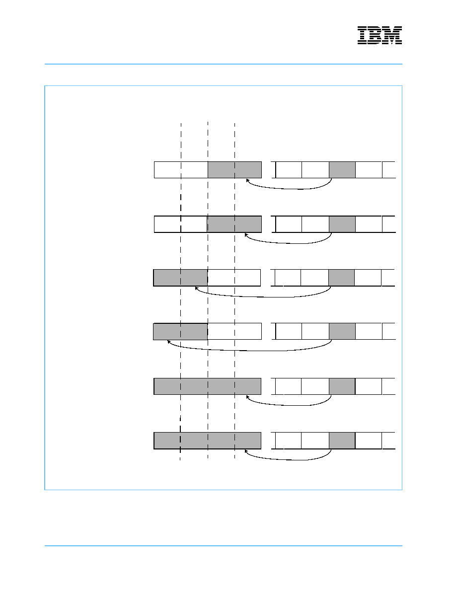
IBM PowerNP NP4GS3
Network Processor
Preliminary
Embedded Processor Complex
Page 204 of 605
np3_ds_sec07_EPC.fm.11
January 29, 2003
Figure 7-6. ot5 Field Definition: Loading GPR Halfword/Word from Array Byte
GPR Word
Register
ot5
Field
Load odd halfword
GPR from
array byte
C
Array
d
d
Load even halfword
GPR from
array byte
D
E
F
Load even halfword
GPR from
array byte
zero extended
Load halfword
GPR from
array byte
sign extended
byte
hw
0
1
d
d
d
d
0
s
d
0
d
s
4
d
d
5
d
d
0
0
0
s
s
s
Load word
GPR from
array byte
zero extended
Load word
GPR from
array byte
sign extended
(hex)
2
3
0
1
zero extended
sign extended

IBM PowerNP NP4GS3
Preliminary
Network Processor
np3_ds_sec07_EPC.fm.11
January 29, 2003
Embedded Processor Complex
Page 205 of 605
Figure 7-7. ot5 FIeld Definition: Store GPR Byte/Halfword/Word to Array Byte/Halfword/Word
GPR Word
Register
ot5
Field
Store byte 3 of
GPR to
array byte
18
Array
d
d
19
1A
1B
byte
hw
0
1
d
d
d
d
d
d
d
d
d
d
10
11
d
d
16
Store byte 2 of
GPR to
array byte
Store byte 1 of
GPR to
array byte
Store byte 0 of
GPR to
array byte
Store odd halfword
GPR to
array halfword
Store even halfword
GPR to
array halfword
Store word
GPR to
array word
(hex)
2
3
0
1

IBM PowerNP NP4GS3
Network Processor
Preliminary
Embedded Processor Complex
Page 206 of 605
np3_ds_sec07_EPC.fm.11
January 29, 2003
7.3.2.1 Memory Indirect Opcode
The memory indirect opcode transfers data between a GPR and a coprocessor array via a logical address in
which the base offset into the array is contained in a GPR. The logical address consists of a coprocessor
number, coprocessor array, base address, and an offset. The C# field indicates the coprocessor which will be
accessed. The Ca field indicates which array of the coprocessor will be accessed. The offset into the array is
the contents of GPR, indicated by Ra as a base plus the six bits of immediate offset, off6. Ra is a half-word
address in the range of 0 - 7. The x indicates whether or not the transaction will be in cell header skip mode.
The memory indirect opcode is executed conditionally if the ALU flags meet the condition represented by the
Cond field. The word address of the GPR register used to transfer or receive data from the array is indicated
by the field R. The actual direction, size, extension format, and location of GPR bytes affected are indicated
by the ot5 field.
pseudocode:
IF (cond) THEN
addr.coprocessor number <= C#
addr.coprocessor array
<= Ca
addr.array offset
<= GPR(Ra)+off6
addr.x_mode
<= x
IF (ot5 = load) THEN
GPR(R,ot5) <= array(addr)
ELSE
array(addr) <= GPR(R,ot5)
END IF;
END IF
Type
31 30 29 28 27 26 25 24 23 22 21 20 19 18 17 16 15 14 13 12 11 10
9
8
7
6
5
4
3
2
1
0
memory
indirect
0
0
1
ot5
Cond
R
x
Ra
C#
Ca
off6
memory add
indirect
0
1
0
ot5
Cond
R
x
Ra
0
0
0
0
off8
memory
direct
0
1
1
ot5
Cond
R
x
0
off2
C#
Ca
off6
scalar
access
0
1
1
ot5
Cond
R
0
1
0
0
C#
Cr
scalar immed
1
1
0
1
C#
Cr
Imm16
transfer
QW
1
1
0
0
C#d
Cad
0
0
QWoffd
0
0
0
0
C#s
Cas
0
1
QWoffs
zero
array
1
1
0
0
0
0
size
Cond
Boffset
x
0
0
0
C#
Ca
1
1
QWoffs

IBM PowerNP NP4GS3
Preliminary
Network Processor
np3_ds_sec07_EPC.fm.11
January 29, 2003
Embedded Processor Complex
Page 207 of 605
7.3.2.2 Memory Address Indirect Opcode
The memory address indirect opcode transfers data between a GPR and a coprocessor data entity (scalar or
array) by mapping the coprocessor logical address into the base address held in the GPR indicated by Ra.
Since not all of the coprocessors have arrays, maximum size arrays, or the maximum number of scalars, the
address map will have many gaps. Data access via this method is the same as access via the more logic-
based method. The final address is formed by the contents of GPR indicated by Ra plus off8 (eight bits). Ra
is a half-word address in the range of 0 - 7. The x indicates whether or not the transaction will be in cell
header skip mode.
The memory address indirect opcode is executed conditionally if the ALU flags meet the condition repre-
sented by the Cond field. The word address of the GPR register used to transfer or receive data from the
array is indicated by the field R. The actual direction, size, extension format, and location of GPR bytes
affected are indicated by the ot5 field.
pseudocode:
IF (cond) THEN
address <= GPR(Ra) + off8
addr.array_notScalar <=
address(14)
addr.coprocessor number <= address(13:10)
addr.coprocessor array
<= address(9:8) (if an array access)
addr.scalar address
<= address(7:0) (if a scalar access)
addr.array offset
<= address(7:0) (if an array access)
addr.x_mode
<= x
IF (ot5 = load) THEN
IF (addr.array_notScalar='1') THEN
GPR(R,ot5) <= array(addr)
ELSE
GPR(R,ot5) <= scalar(addr)
END IF;
ELSE
IF (addr.array_notScalar='1') THEN
array(addr) <= GPR(R,ot5)
ELSE
scalar(addr) <= GPR(R,ot5)
END IF;
END IF;
END IF

IBM PowerNP NP4GS3
Network Processor
Preliminary
Embedded Processor Complex
Page 208 of 605
np3_ds_sec07_EPC.fm.11
January 29, 2003
7.3.2.3 Memory Direct Opcode
The memory direct opcode transfers data between a GPR and a coprocessor array via a logical address that
is specified in the immediate portion of the opcode. The logical address consists of a coprocessor number,
coprocessor array, and an offset. The C# field indicates the coprocessor that is accessed. The Ca field indi-
cates which array of the coprocessor is accessed. The offset is made up of eight bits: the most significant two
bits are located in field off2 and the remaining six bits are in off6. The x indicates whether or not the transac-
tion will be in cell header skip mode. The memory direct opcode is executed conditionally if the ALU flags
meet the condition represented by the Cond field. The word address of the GPR register used to transfer or
receive data from the array is indicated by the R field. The actual direction, size, extension format, and loca-
tion of GPR bytes affected are indicated by the ot5 field.
pseudocode:
IF (cond) THEN
addr.coprocessor number <= C#
addr.coprocessor array
<= Ca
addr.array offset
<= off2&off6
addr.x_mode
<= x
IF (ot5 = load) THEN
GPR(R,ot5) <= array(addr)
ELSE
array(addr) <= GPR(R,ot5)
END IF;
END IF
7.3.2.4 Scalar Access Opcode
The scalar access opcode transfers data between a GPR and a scalar register via a logical address that con-
sists of a coprocessor number and a scalar register number. The C# field indicates the coprocessor that is
accessed. The scalar register number is indicated by the Cr field. The scalar access opcode is executed con-
ditionally if the ALU flags meet the condition represented by the Cond field. The word address of the GPR
register used to transfer or receive data from the scalar register is indicated by the R field. The actual direc-
tion, size, extension format, and location of GPR bytes affected are indicated by the ot5 field.
pseudocode:
IF (cond) THEN
addr.coprocessor number <= C#
addr.scalar number
<= Ca
IF (ot5 = load) THEN
GPR(R,ot5) <= scalar(addr)
ELSE
scalar(addr) <= GPR(R,ot5)
END IF;
END IF

IBM PowerNP NP4GS3
Preliminary
Network Processor
np3_ds_sec07_EPC.fm.11
January 29, 2003
Embedded Processor Complex
Page 209 of 605
7.3.2.5 Scalar Immediate Opcode
The scalar immediate opcode writes immediate data to a scalar register via a logical address that is com-
pletely specified in the immediate portion of the opcode. The logical address consists of a coprocessor num-
ber and a coprocessor register number. The C# field indicates the coprocessor that is accessed. The Cr field
indicates the scalar register number. The data to be written is the Imm16 field.
pseudocode:
addr.coprocessor number
<= C#
addr.scalar register number <= Ca
scalar(addr) <= Imm16
7.3.2.6 Transfer Quadword Opcode
The transfer quadword opcode transfers quadword data from one array location to another using one instruc-
tion. The source quadword is identified by the C#s (coprocessor number), Cas (source array number), and
QWoffs (quadword offset into the array). The destination quadword is identified by the C#d, Cad, and
QWoffd.This transfer is only valid on quadword boundaries.
pseudocode:
saddr.coprocessor number <= C#s
saddr.array number
<= Cas
saddr.quadword offset
<= QWoffs
daddr.coprocessor number <= C#d
daddr.array number
<= Cad
daddr.quadword offset
<= QWoffd
array(daddr) <= array(saddr)

IBM PowerNP NP4GS3
Network Processor
Preliminary
Embedded Processor Complex
Page 210 of 605
np3_ds_sec07_EPC.fm.11
January 29, 2003
7.3.2.7 Zero Array Opcode
The zero array opcode zeroes out a portion of an array with one instruction. The size of the zeroed-out por-
tion can be a byte, halfword, word, or quadword. Quadword access must be on quadword address bound-
aries. Accesses to a byte, halfword, or word can begin on any byte boundary and will have the same
characteristics as any GPR-based write to the array. For example, if the array is defined to wrap from the end
to the beginning, the zero array command wraps from the end of the array to the beginning. The C# field indi-
cates the coprocessor that will be accessed. The Ca field indicates which array of the coprocessor is
accessed. The QWoff is the quadword offset into the array, and the Boff is the byte offset into the array. The
x indicates whether or not the transaction is in cell header skip mode. The opcode is executed conditionally if
the ALU flags meet the condition represented by the Cond field. The actual size of the access is defined by
the size field (byte = 00, halfword = 01, word = 10, quadword = 11). For quadword accesses Boff should equal
0x0.
pseudocode:
IF (cond) THEN
addr.coprocessor number <= C#
addr.array number
<= Ca
addr.quadword offset
<= QWoff
addr.byte offset
<= Boff
IF size = 00 THEN
array(addr) <= 0x00
IF size = 01 THEN
array(addr : addr+1) <= 0x0000
IF size = 10 THEN
array(addr : addr+3) <= 0x00000000
IF size = 11 THEN
array(addr : addr+15) <= 0x0000000000000000000000000000000
END IF;
IBM PowerNP NP4GS3
Preliminary
Network Processor
np3_ds_sec07_EPC.fm.11
January 29, 2003
Embedded Processor Complex
Page 211 of 605
7.3.3 Coprocessor Execution Opcodes
The coprocessor execution opcodes are used to initiate operations or synchronize operations with the copro-
cessors. The execution type opcodes initiate accesses on the processor execution interface (PEI). A com-
mand to a coprocessor consists of six bits of coprocessor operation and 44 bits of coprocessor arguments.
The definition of the operation and argument bits is coprocessor dependent.
A coprocessor can operate synchronously or asynchronously. Synchronous operation means the execution
of the thread initiating the coprocessor command stalls until the coprocessor operation is complete. Asyn-
chronous operation means the executing thread will not stall when a coprocessor execution command is
issued, but rather can continue operating on the instruction stream. It is important to re-synchronize a copro-
cessor command that was issued asynchronously before using resources that the coprocessor needs for
execution of the command. This can be done with the "wait" coprocessor execution opcodes.
The CLP runs the instruction stream of two threads in which only one thread can actually execute in a given
cycle. The CLP thread that owns priority cannot be stalled by the execution of the non-priority thread. Priority
is granted to the only active thread in a CLP or to the thread that is given priority by the other thread. The
coprocessor execution opcodes indicated by the P bit in the following opcode map can give up the priority
status of the thread.
Type
31 30 29 28 27 26 25 24 23 22 21 20 19 18 17 16 15 14 13 12 11 10 9
8
7
6
5
4
3
2
1
0
execute
direct
1
1
1
1
C#
p
CPop
a
0
Imm16
execute
indirect
1
1
1
1
C#
p
CPop
a
1
R
Imm12
execute
direct
conditional
1
1
1
0
C#
Cond
op
0
1
Imm16
execute
indirect
conditional
1
1
1
0
C#
Cond
op
1
1
R
Imm12
wait
1
1
1
0
0
0
0
0
p
0
0
0
0
0
0
0
mask16
wait and
branch
1
1
1
0
C#
p
0
0
0
1
0
ok
0
Target16

IBM PowerNP NP4GS3
Network Processor
Preliminary
Embedded Processor Complex
Page 212 of 605
np3_ds_sec07_EPC.fm.11
January 29, 2003
7.3.3.1 Execute Direct Opcode
The execute direct opcode initiates a coprocessor command in which all of the operation arguments are
passed immediately to the opcode. The C# field indicates which coprocessor will execute the command. The
CPopfield is the coprocessor operation field. The Imm16 field contains the operation arguments that are
passed with the command. The a field indicates whether the command should be executed asynchronously.
The p field indicates if the thread should give up priority.
pseudocode:
exe.coprocessor number
<= C#
exe.coprocessor operation
<= CPop
exe.coprocessor arguments <= "0000000000000000000000000000" & Imm16
coprocessor <= exe
IF a=1 THEN
PC <= PC+1
ELSE
PC <= stall
END IF
IF p=1 THEN
PriorityOwner(other thread)<= TRUE
ELSE
PriorityOwner(other thread)<= PriorityOwner(other thread)
END IF;

IBM PowerNP NP4GS3
Preliminary
Network Processor
np3_ds_sec07_EPC.fm.11
January 29, 2003
Embedded Processor Complex
Page 213 of 605
7.3.3.2 Execute Indirect Opcode
The execute indirect opcode initiates a coprocessor command in which the operation arguments are a combi-
nation of a GPR register and an immediate field. The field C# indicates which coprocessor the command is to
be executed on. The field CPop is the coprocessor operation field. The R field is the GPR register to be
passed as part of the operation arguments. The Imm12 field contains the immediate operation arguments
that are passed. The a field indicates whether the command should be executed asynchronously. The p field
indicates if the thread should give up priority.
pseudocode:
exe.coprocessor number
<= C#
exe.coprocessor operation
<= CPop
exe.coprocessor arguments <= Imm12 & GPR(R)
coprocessor <= exe
IF a=1 THEN
PC <= PC+1
ELSE
PC <= stall
END IF
IF p=1 THEN
PriorityOwner(other thread)<= TRUE
ELSE
PriorityOwner(other thread)<= PriorityOwner(other thread)
END IF;
7.3.3.3 Execute Direct Conditional Opcode
The execute direct conditional opcode is similar to the execute direct opcode except that the execute direct
conditional opcode command can be issued conditionally based on the Cond field. To make room in the
opcode for the Cond field, the coprocessor opcode field (op) is shortened to two bits. Because the high order
four bits of the coprocessor operation are assumed to be zeros, conditional operations are restricted to the
lower four commands of a coprocessor. he command is assumed to be synchronous because the opcode
does not have a bit to indicate whether it is asynchronous or synchronous. Priority cannot be released with
this opcode.
pseudocode:
IF (Cond) THEN
exe.coprocessor number
<= C#
exe.coprocessor operation
<= "0000"&op
exe.coprocessor arguments <= "0000000000000000000000000000" & Imm16
coprocessor <= exe
END IF

IBM PowerNP NP4GS3
Network Processor
Preliminary
Embedded Processor Complex
Page 214 of 605
np3_ds_sec07_EPC.fm.11
January 29, 2003
7.3.3.4 Execute Indirect Conditional Opcode
The execute indirect conditional opcode is similar to the execute indirect opcode except that the execute indi-
rect command can be issued conditionally based on the Cond field. To make room in the opcode for the Cond
field, the coprocessor opcode field (op) is shortened to two bits. Because the high order four bits of the copro-
cessor operation are assumed to be 0s, conditional operations are restricted to the lower four commands of a
coprocessor. The command is assumed to be synchronous because the opcode does not have a bit to indi-
cate whether it is asynchronous or synchronous. Priority cannot be released with this opcode.
pseudocode:
IF (Cond) THEN
exe.coprocessor number
<= C#
exe.coprocessor operation
<= "0000"&op
exe.coprocessor arguments <= Imm12 & GPR(R)
coprocessor <= exe
END IF
7.3.3.5 Wait Opcode
The wait opcode synchronizes one or more coprocessors. The mask16 field (see the register bit list table in
Section 7.3.3 on page 211) is a bit mask (one bit per coprocessor) in which the bit number corresponds to the
coprocessor number. The thread stalls until all coprocessors indicated by the mask complete their operations.
Priority can be released with this command.
pseudocode:
IF Reduction_OR(mask16(i)=coprocessor.busy(i)) THEN
PC <= stall
ELSE
PC <= PC + 1
END IF
IF p=1 THEN
PriorityOwner(other thread)<= TRUE
ELSE
PriorityOwner(other thread)<= PriorityOwner(other thread)
END IF;

IBM PowerNP NP4GS3
Preliminary
Network Processor
np3_ds_sec07_EPC.fm.11
January 29, 2003
Embedded Processor Complex
Page 215 of 605
7.3.3.6 Wait and Branch Opcode
The wait and branch opcode synchronizes with one coprocessor and branch on its one bit OK/KO flag. This
opcode causes the thread to stall until the coprocessor represented by C# is no longer busy. The OK/KO flag
is then compared with the field OK. If they are equal, the thread branches to the address in the target16 field.
Priority can be released with this command.
pseudocode:
IF coprocessor.busy(C#)=1 THEN
PC <= stall
ELSIF coprocessor.ok(C#)=ok THEN
PC <= target16
ELSE
PC <= PC+1
END IF
IF p=1 THEN
PriorityOwner(other thread)<= TRUE
ELSE
PriorityOwner(other thread)<= PriorityOwner(other thread)
END IF;

IBM PowerNP NP4GS3
Network Processor
Preliminary
Embedded Processor Complex
Page 216 of 605
np3_ds_sec07_EPC.fm.11
January 29, 2003
7.3.4 ALU Opcodes
ALU opcodes are used to manipulate GPR registers with arithmetic and logical functions. All of these
opcodes execute in a single cycle. These opcodes are also used to manipulate the ALU status flags used in
condition execution of opcodes. All ALU opcodes are executed conditionally based upon the Cond field.
7.3.4.1 Arithmetic Immediate Opcode
The arithmetic immediate opcode performs an arithmetic function on a GPR register in which the second
operand is a 12-bit immediate value. The word GPR operand and destination GPR are specified in the R field
and the immediate operand is represented by Imm4&Imm8. The actual portion of the GPR and extension of
the immediate operand are shown in the ot3i table. The arithmetic function performed is given in the AluOp
field. This AluOp functions of AND, OR, XOR, TST, and COMPARE are not used with this opcode and have a
different opcode when the second operand is an immediate value. Arithmetic opcodes can be performed
without changing the ALU status flags if the i field is a 1.
pseudocode:
IF (Cond) THEN
alu.opr1
<= GPR(R,ot3i)
alu.opr2 <=
ot3i(Imm4&Imm8)
GPR(R,ot3i) <= Aluop.result(alu.opr1,alu.opr2)
IF (i=0) THEN
AluStatus <= Aluop.flags(alu.opr1, alu.opr2)
END IF
END IF
Type
31 30 29 28 27 26 25 24 23 22 21 20 19 18 17 16 15 14 13 12 11 10
9
8
7
6
5
4
3
2
1
0
Arithmetic
Immediate
1
0
0
0
i
ot3i
Cond
R
Imm12(11:8)
AluOp
Imm12(7:0)
Logical
Immediate
1
0
0
1
i
h
Lop
Cond
R
Imm16
Compare
Immediate
1
0
1
0
0
0
ot2i
Cond
R
Imm16
Load
Immediate
1
0
1
1
ot4i
Cond
R
Imm16
Arithmetic/
Logical
Register
1
1
0
0
i
ot3r
Cond
Rd
Rs
AluOp
0
0
0
0
w
h
n
m
Count
Leading
Zeros
1
0
1
0
1
hd
w
i
Cond
Rd
Rs
0
0
0
0
0
0
0
0
0
h
n
0

IBM PowerNP NP4GS3
Preliminary
Network Processor
np3_ds_sec07_EPC.fm.11
January 29, 2003
Embedded Processor Complex
Page 217 of 605
Table 7-4. AluOp Field Definition
AluOp
Function
Pseudocode
Flags Modified
Z
C
N
V
0000
add
result = opr1 + opr2
x
x
x
x
0001
add
w/carry
result = opr1 + opr2 + C
x
x
x
x
0010
subtract
result = opr1 - opr2
x
x
x
x
0011
subtract w/carry
result = opr1 - opr2 - C
x
x
x
x
0100
xor
result = orp1 XOR opr2
x
x
0101
and
result = opr1 AND opr2
x
x
0110
or
result = opr1 OR opr2
x
x
0111
shift left
logical
result = opr1
<-opr2
, fill with 0s
C = C when opr2 = 0 else
C = 0 when opr2 > n else
C = opr1(n - opr2); where n = size of opr1
x
x
x
1000
shift right logical
result = fill with 0, opr1
->opr2
C = C when opr2 = 0 else
C = 0 when opr2 > n else
C = opr1(opr2 - 1); where n = size of opr1
x
x
x
1001
shift right
arithmetic
result = fill with S, opr1
->opr2
C = C when opr2 = 0 else
C = opr1(n - 1) when opr2 > n else
C = opr1(opr2 - 1); where n = size of opr1
x
x
x
1010
rotate right
result = fill with opr1, opr1
->opr2
C = C when opr 2 = 0 else
C= opr1(MODn(opr2 - 1)); where n = size of opr1
x
x
x
1011
compare
opr1 - opr2
x
x
x
x
1100
test
opr1 AND opr2
x
x
1101
not
result = NOT(opr1)
x
x
1110
transfer
result = opr2
1111
reserved
reserved

IBM PowerNP NP4GS3
Network Processor
Preliminary
Embedded Processor Complex
Page 218 of 605
np3_ds_sec07_EPC.fm.11
January 29, 2003
Figure 7-8. ot3i Field Definition
GPR Register
ot3i
Field
Odd halfword GPR,
0
Imm12
Imm12
Imm12
1
2
3
0
s
byte
hw
0
1
Imm12
0
0
0
Imm12
1
Imm12
s
s
Immediate field with
0 extend
Even halfword GPR,
Immediate field with
0 extend
Odd halfword GPR,
Immediate field with
sign extend
Even halfword GPR,
Immediate field with
sign extend
Word GPR,
Immediate field with
0 extend
Word GPR,
Immediate field with
sign extend
0
1
2
3

IBM PowerNP NP4GS3
Preliminary
Network Processor
np3_ds_sec07_EPC.fm.11
January 29, 2003
Embedded Processor Complex
Page 219 of 605
7.3.4.2 Logical Immediate Opcode
The logical immediate opcode performs the logical functions AND, OR, XOR, and TEST on a GPR register in
which the second operand is a 16-bit immediate value. the R field specifies the word GPR operand and desti-
nation GPR, and the h field specifies the even (h = 0) or odd (h = 1) halfword of this GPR. The immediate
operand is represented by Imm16. The arithmetic function performed is given in the Lop field. Logical
opcodes can be performed without changing the ALU status flags if the i field is a 1.
pseudocode:
IF (Cond) THEN
alu.opr1
<= GPR(R:h)
alu.opr2 <=
Imm16
GPR(R:h) <= Lop.result(alu.opr1,alu.opr2)
IF (i=0) THEN
AluStatus <= Lop.flags(alu.opr1, alu.opr2)
END IF
END IF
7.3.4.3 Compare Immediate Opcode
The compare immediate opcode performs the compare functions on a GPR register in which the second
operand is a 16-bit immediate value. The source GPR operand and destination GPR are specified in the R
field, and the immediate operand is represented by Imm16. The actual portion of the GPR and extension of
the immediate operand are shown in Figure 7-9. The compare immediate opcode always changes the ALU
status flags.
pseudocode:
IF (Cond) THEN
alu.opr1
<= GPR(R,ot2i)
alu.opr2 <=
ot2i(Imm16)
AluStatus <= compare(alu.opr1, alu.opr2)
END IF
Table 7-5. Lop Field Definition
LOp
Function
Pseudocode
Flags Modified
Z
C
N
V
00
xor
result = orp1 XOR opr2
x
x
01
and
result = opr1 AND opr2
x
x
10
or
result = opr1 OR opr2
x
x
11
test
opr1 AND opr2
x
x

IBM PowerNP NP4GS3
Network Processor
Preliminary
Embedded Processor Complex
Page 220 of 605
np3_ds_sec07_EPC.fm.11
January 29, 2003
7.3.4.4 Load Immediate Opcode
The operation arguments of the load immediate opcode are a combination of a GPR register and a 16-bit
immediate field. The source GPR operand and destination GPR are specified by the R field and the immedi-
ate operand is represented by Imm16. The actual portion of the GPR and extension of the immediate oper-
and are shown in Figure 7-10 and Figure 7-11. Load immediate opcode never changes the ALU status flags if
executed.
pseudocode:
IF (Cond) THEN
GPR(R,ot4i) <= ot4i(Imm16)
END IF
Figure 7-9. ot2i Field Definition: Compare Halfword/Word Immediate
GPR Register
ot2i
Field
Compare odd GPR
register with
Immediate data
0
Imm16
Imm16
Compare even GPR
register with
Immediate data
Imm16
Imm16
1
2
3
Compare word GPR
register with
Immediate data
zero extend
0
s
Compare word GPR
register with
immediate data
sign extend
byte
hw
0
1
0
1
2
3

IBM PowerNP NP4GS3
Preliminary
Network Processor
np3_ds_sec07_EPC.fm.11
January 29, 2003
Embedded Processor Complex
Page 221 of 605
Figure 7-10. ot4i Field Definition Load Immediate Halfword/Word
GPR Register
ot5
Field
Load odd halfword
GPR from
Immediate data
0
Imm16
Load even halfword
GPR from
Immediate data
1
Load word GPR
from
Immediate data
zero extended
Load word GPR
from
immediate data
0 postpend
Load word GPR
from
immediate data
byte
hw
0
1
2
6
Imm16
Imm16
Imm16
4
Imm16
1 extended
5
Imm16
Load word GPR
from
immediate data
1 postpend
3
Imm16
Load word GPR
from
immediate data
sign extended
s
1
1
0
0
0
1
2
3
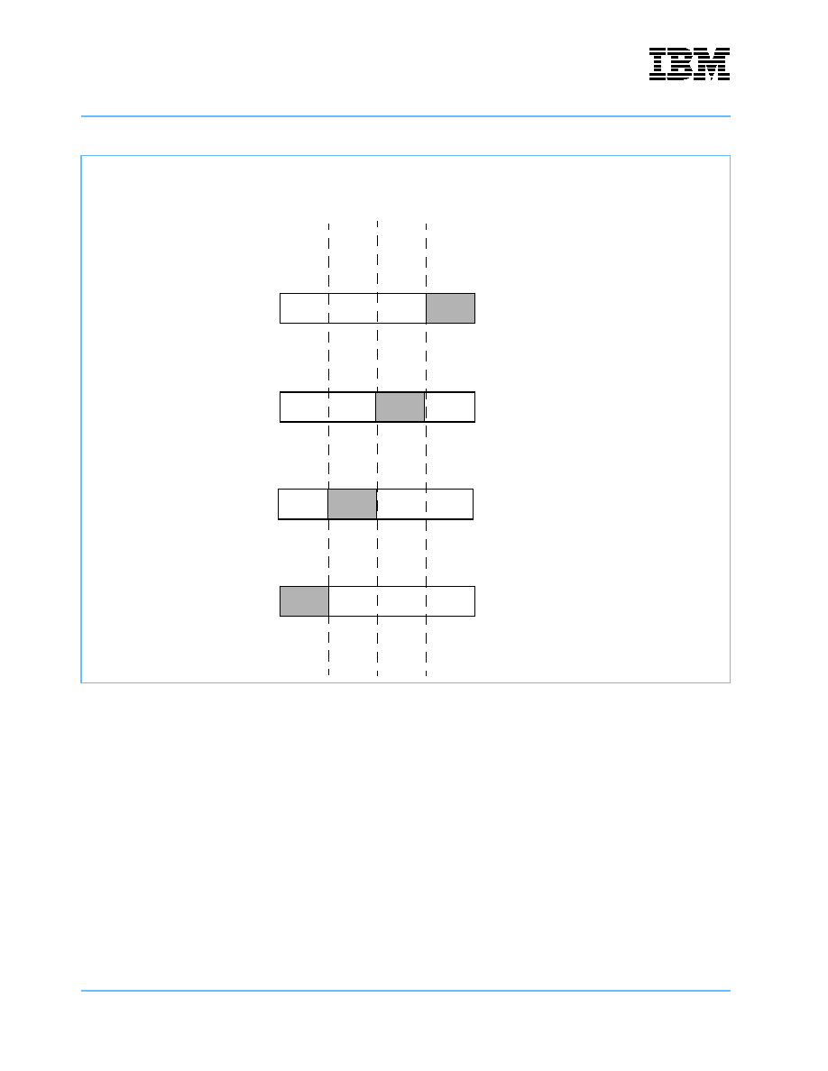
IBM PowerNP NP4GS3
Network Processor
Preliminary
Embedded Processor Complex
Page 222 of 605
np3_ds_sec07_EPC.fm.11
January 29, 2003
Figure 7-11. ot4i Field Definition: Load Immediate Byte
ot4i
Field
Load GPR byte 3
from low byte of
immediate data
8
d
Load GPR byte 2
from low byte of
9
A
B
Load GPR byte 1
from low byte of
immediate data
Load GPR byte 0
from low byte of
immediate data
byte
hw
0
1
d
d
d
immediate data
GPR Register
0
1
2
3

IBM PowerNP NP4GS3
Preliminary
Network Processor
np3_ds_sec07_EPC.fm.11
January 29, 2003
Embedded Processor Complex
Page 223 of 605
7.3.4.5 Arithmetic Register Opcode
The arithmetic register opcode performs an arithmetic function on a GPR register in which the second oper-
and is also a GPR register. The first GPR operand and the destination GPR are specified by the word
address R1 and the specific portion to be used is encoded in ot3r. The second operand source is represented
by word address R2 with the h field determining the even or odd halfword if the ot3r field indicates a halfword
is needed. If the AluOp is a shift or rotate command, the second operand source is used as the amount of the
shift or rotate. Otherwise, ot3r indicates the relationship between the two operands. If the AluOp is a logical
operation (AND, OR, XOR, TEST), the second operand source can then further be modified by the m and n
fields. The m field is the mask field and, if active, creates a 1-bit mask in which the "1" bit is represented by
the second operand source. The n field is the invert field and, if active, will invert the second operand source.
If both the m and n fields are "1", the mask is created before the inversion. Table 7-6 show how to use these
fields to create other operations from the basic logic commands. The arithmetic function performed is given in
the AluOp field. Arithmetic opcodes can be performed without changing the ALU status flags if the "i" field is a
1. Arithmetic opcodes can be performed without writing back the data if the "w" field is a 1.
pseudocode:
IF (Cond) THEN
alu.opr1
<= GPR(R1,ot3r)
alu.opr2 <=
GPR(R2,h)
IF `m'='1' THEN
alu.opr2 <= bitmask(alu.opr2)
END IF
IF `n'='1' THEN
alu.opr2 <= NOT(alu.opr2)
END IF
IF `w'='0' THEN
GPR(R2,ot3i) <= Aluop.result(alu.opr1,alu.opr2)
END IF
IF (i=0) THEN
AluStatus <= Aluop.flags(alu.opr1, alu.opr2)
END IF
END IF
Table 7-6. Arithmetic Opcode Functions
Function
AluOp
m
n
Bit clear
AND
1
1
Bit set
OR
1
0
Bit flip
XOR
1
0

IBM PowerNP NP4GS3
Network Processor
Preliminary
Embedded Processor Complex
Page 224 of 605
np3_ds_sec07_EPC.fm.11
January 29, 2003
Figure 7-12. ot3r Field Definition
GPR (R1) Register
ot3r
Field
odd halfword of
0
gpr2
even halfword of
GPR R1 is operand1
GPR R2 is a halfword
gpr2
gpr2
1
2
3
word GPR R1 is
operand 1
zero extended
0
s
word GPR R1 is
operand 1
GPR R2 is halfword
zero extend
gpr2
word GPR R1 is
operand 1
GPR R2 is a word
byte
hw
0
1
6
GPR R1 is operand1
GPR R2 is a halfword
GPR R2 is halfword
operand
gpr2
0
1
2
3

IBM PowerNP NP4GS3
Preliminary
Network Processor
np3_ds_sec07_EPC.fm.11
January 29, 2003
Embedded Processor Complex
Page 225 of 605
7.3.4.6 Count Leading Zeros Opcode
The count leading zeros opcode returns the number of zeros from left to right until the first 1-bit is encoun-
tered. This operation can be performed on a halfword or word GPR register. There is a second variation of
this command in which the return value of this command is the bit position of the first "1" from left to right in
the GPR. The GPR to be analyzed is determined by the R fields. If the GPR is a halfword instruction, the h
field indicates whether the even or odd half is used. The destination register is always a halfword register and
is represented by the Rd field and halfword indicator `hd'. The w field indicates whether the operation is a
word or halfword. The n field determines if the command counts the number of leading zeros (n = 0) or if the
command returns the bits position of the first one (n = 1). The only flag for this command is the overflow flag,
which is set if the GPR being tested contains all zeros. The setting of this flag can be inhibited if the i field is a
one.
pseudocode:
IF (Cond) THEN
alu.opr1
<= GPR(Rs,h)
alu.result <= count_zero_left_to_right(alu.opr1)
IF `n'='1' THEN
GPR(Rd,hd) <= NOT(alu.result)
ELSE
GPR(Rd,hd) <= alu.result
END IF
IF (i=0) THEN
AluStatus <= Aluop.flags(alu.opr1, alu.opr2)
END IF
END IF

IBM PowerNP NP4GS3
Network Processor
Preliminary
Embedded Processor Complex
Page 226 of 605
np3_ds_sec07_EPC.fm.11
January 29, 2003
7.4 DPPU Coprocessors
Each DPPU coprocessor is a specialized hardware assist engine that runs in parallel with the two CLPs and
performs functions that would otherwise require a large amount of serialized picocode. DPPU functions
include modifying IP headers, maintaining flow information used in flow control algorithms, accessing internal
registers via the CAB, maintaining counts for flow control and for standard and proprietary Management Infor-
mation Blocks (MIB), and enqueueing frames to be forwarded.
The DPPU coprocessors are:
A thread's address space is a distributed model in which registers and arrays reside within the coprocessors
(each coprocessor maintains resources for four threads and, for address mapping purposes, the CLP is
considered to be a coprocessor). Each coprocessor can have a maximum of 252 scalar registers and four
arrays.
The address of a scalar register or array within the DPPU becomes a combination of the coprocessor number
and the address of the entity within the coprocessor. Likewise, the coprocessor instruction is a combination of
the coprocessor number and the coprocessor opcode.
The EPC coprocessors are numbered as shown in Table 7-7. The number is used in accesses on both the
coprocessor execute and data interfaces. The TSE is mapped to two coprocessor locations so that a thread
can execute two searches simultaneously.
Tree Search Engine
See Section 8. Tree Search Engine on page 311.
Data Store
See Section 7.4.2 beginning on page 227.
Control Access Bus (CAB) Interface
See Section 7.4.3 beginning on page 244.
Enqueue See
Section 7.4.4 beginning on page 247.
Checksum See
Section 7.4.5 beginning on page 266.
String Copy
See Section 7.4.6 beginning on page 271.
Policy See
Section 7.4.7 beginning on page 272.
Counter See
Section 7.4.8 beginning on page 273.
Coprocessor Response Bus
See Section 7.4.9 beginning on page 277.
Semaphore
See Section 7.4.10 beginning on page 278.

IBM PowerNP NP4GS3
Preliminary
Network Processor
np3_ds_sec07_EPC.fm.11
January 29, 2003
Embedded Processor Complex
Page 227 of 605
7.4.1 Tree Search Engine Coprocessor
The Tree Search Engine (TSE) coprocessor has commands for tree management, direct access to the
Control Store (CS), and search algorithms such as full match (FM), longest prefix match (LPM), and software-
managed tree (SMT).
For complete information, see Section 8. Tree Search Engine on page 311.
7.4.2 Data Store Coprocessor
The Data Store coprocessor provides an interface between the EPC and the Ingress Data Store, which
contains frames that have been received from the media, and the Egress Data Store, which contains reas-
sembled frames received from the switch interface. The Data Store coprocessor also receives configuration
information during the dispatch of a timer event or interrupt.
Each thread supported by the Data Store coprocessor has one set of scalar registers and arrays defined for
it. The scalar registers control the accesses between the shared memory pool and the ingress and egress
data stores. The Data Store coprocessor maintains them. The arrays are defined in the shared memory pool
(see 7.2.4 Shared Memory Pool on page 196):
� The DataPool, which can hold eight quadwords
� Two scratch memory arrays, which hold eight and four quadwords respectively
� The configuration quadword array, which holds port configuration data dispatched to the thread.
The shared memory pool arrays function as a work area for the Data Store coprocessor: instead of reading or
writing small increments (anything less than a quadword, or 16 bytes) directly to a data store, a larger amount
(one to four quadwords per operation) of frame data is read from the data store into these shared memory
pool arrays or from the these arrays into the data store.
The Data Store coprocessor has nine commands available to it. These commands are detailed in Section
7.4.2.2 Data Store Coprocessor Commands on page 234.
Table 7-7. Coprocessor Instruction Format
Coprocessor Number
Coprocessor
0
Core Language Processor (CLP)
1
Data Store Interface
2
Tree Search Engine 0
3
Tree Search Engine 1
4
CAB Interface
5
Enqueue
6
Checksum
7
String Copy
8
Policy
9
Counter
10
Coprocessor Response Bus (CRB)
11
Semaphore

IBM PowerNP NP4GS3
Network Processor
Preliminary
Embedded Processor Complex
Page 228 of 605
np3_ds_sec07_EPC.fm.11
January 29, 2003
7.4.2.1 Data Store Coprocessor Address Map
Table 7-8. Data Store Coprocessor Address Map
(A thread's scalar registers and arrays that are mapped within the
Data Store coprocessor) (Page 1 of 2)
Name
Register
(Array)
1
Number
Size
(bits)
Access
Description
DSA
x`00'
19
R/W
Address of Ingress or Egress Data Store. Used in all commands
except "read more" and "dirty". (Ingress uses the least significant 11
bits and Egress uses all 19 bits for the address.)
LMA
x`01'
6
R/W
Quadword address of Shared Memory Pool. Used in all commands
except "read more". (See 7.2.4 Shared Memory Pool on page 196.)
CCTA
x`02'
19
R/W
Current address of the ingress data buffer or the egress twin that was
dispatched to the thread into the datapool. Used in "read more" and
"dirty" commands. The value is unitized at dispatch and updated on
"read more" commands that pass though cell or twin boundaries.
NQWA
x`03'
3
R/W
Indicates the QW address used for both the Datapool and the QW in
the datastore buffer/twin. See EDIRTY (Update Egress Dirty Quad-
words) Command on page 242, IDIRTY (Update Ingress Dirty Quad-
words) Command on page 243, RDMOREE (Read More Quadword
From Egress) Command on page 239, and RDMOREI (Read More
Quadword From Ingress) Command on page 241 for details.
iProtocolType
x`04'
16
R
Layer 3 Protocol identifier set by the hardware classifier (see 7.7
Hardware Classifier on page 289).
DirtyQW
x`05'
8
R/W
Quadwords in the DataPool that have been written and therefore may
not be equivalent to the corresponding Data Store data. Used by the
dirty update commands to write back any modified data into the corre-
sponding Data Store.
BCI2Byte
x`06'
14/20
R/W
A special-purpose register. The picocode running in the CLP writes a
BCI value, but when the register is read, it returns the 14-bit byte
count represented by the BCI.
In NP4GS3C (R3.x), the format of the BCI can be changed by config-
uration (see Section 13.3 TB Mode Register (TB_Mode) on page
473). The BCI value input to this register must match the configured
format.
Disp_DSU
x`07'
2
R/W
Initialized during dispatch to contain the same value as the DSU field
in the Egress FCBPage. This register is used by Egress write com-
mands to determine which Egress Data Store the Data Store copro-
cessor should access when writing data.
This register has no meaning for Ingress frames.
Disp_DSUSel
x`08'
1
R/W
Initialized during dispatch to contain the same value as the DSU_Sel
field in the Egress FCBPage. This register is used by Egress read
commands to determine which Egress Data Store the Data Store
coprocessor should access when reading data.
This register has no meaning for Ingress frames.
Disp_Ingress
x`09'
1
R
Dispatched frame's type
0
Egress frame
1
Ingress frame
1. A number in parentheses is the array number for this coprocessor. Each array has a register number and an array number.

IBM PowerNP NP4GS3
Preliminary
Network Processor
np3_ds_sec07_EPC.fm.11
January 29, 2003
Embedded Processor Complex
Page 229 of 605
The DataPool and Data Store Access
Upon frame dispatch, the Dispatch Unit automatically copies the first N quadwords of a frame from the Data
Store into the first N quadword positions of the DataPool. The value of N is programmable in the Port Config-
uration Memory. Typically, values of N are as follows:
The read more commands (RDMOREI and RDMOREE) assist the picocode's reading of additional bytes of a
frame by automatically reading the frame data into the DataPool at the next quadword address and wrapping
automatically to quadword 0 when the boundary of the DataPool is reached. The picocode can also read or
write the Ingress and Egress Data Stores at an absolute address, independent of reading sequential data
after a dispatch.
BCI2Byte_WChk
x`0E'
24
W
In NP4GS3C (R3.x), the BCI2Byte_WChk write only register is added.
BCI values (the format of which can be configured (see Section 13.3
TB Mode Register (TB_Mode) on page 473)) written to this register
are checked and a byte count value is generated. The results are read
from the BC2Byte register. When an invalid BCI value is written, a
result of zero is returned.
An invalid BCI is defined in one of the following ways:
�
Number of data buffers (weight) = 0
�
Number of data buffers (weight) = 1 and
ending byte location < starting byte location
�
Starting byte location or ending byte location < 6
ConfigQW
x`FC'
(0)
128
R/W
Port Configuration Table Entry for this frame
ScratchMem0
x`FD'
(1)
512
R/W
User Defined Array (use to store temporary information, build new
frames, and so on)
ScratchMem1
x`FE'
(2)
1024
R/W
User Defined Array (use to store temporary information, build new
frames, and so on)
DataPool
x`FF'
(3)
1024
R/W
Contains frame data from the Dispatch Unit
N = 4
Ingress frame dispatch
N = 2
Egress unicast frame dispatch
N = 4
Egress multicast frame dispatch
N = 0
Interrupts and timers
Table 7-8. Data Store Coprocessor Address Map
(A thread's scalar registers and arrays that are mapped within the
Data Store coprocessor) (Page 2 of 2)
Name
Register
(Array)
1
Number
Size
(bits)
Access
Description
1. A number in parentheses is the array number for this coprocessor. Each array has a register number and an array number.

IBM PowerNP NP4GS3
Network Processor
Preliminary
Embedded Processor Complex
Page 230 of 605
np3_ds_sec07_EPC.fm.11
January 29, 2003
The DataPool for Ingress Frames
For an Ingress Dispatch, the N quadwords are stored in the DataPool at quadword-address 0, 1, ... N - 1.
Each quadword contains raw frame-bytes, (there are no cell header or frame headers for ingress frames in
the DataPool). After an Ingress Dispatch, the DataPool contains the first N*16 bytes of the frame, where the
first byte of the frame has byte address 0. The Ingress DataPool Byte Address Definitions are listed in Table
7-9.
When reading more than N quadwords of a frame (using the RDMOREI command), the hardware automati-
cally walks the Data Store's buffer control block (BCB) chain as required. Quadwords read from the Data
Store are written to the DataPool at consecutive quadword-locations, starting at quadword address N (where
N is the number of quadwords written to the DataPool by the Dispatch Unit during frame dispatch). The quad-
word-address wraps from 7 - 0. Therefore, the picocode must save quadword 0 in case it is required later (for
example, the quadword can be copied to a scratch array).
The Ingress Data Store can also be written and read with an absolute address. The address is a BCB
address.
Reading from an absolute address can be used for debugging and to inspect the contents of the Ingress DS.
For absolute Ingress Data Store access (reads and writes), the picocode must provide the address in the
Ingress Data Store, the quadword address in the DataPool, and the number of quadwords to be transferred.
Figure 7-13 shows an example of a frame stored in the Ingress Data Store:
Table 7-9. Ingress DataPool Byte Address Definitions
Quadword
Byte Address
0
0
1
2
3
4
5
6
7
8
9
10
11
12
13
14
15
1
16
17
18
19
20
21
22
23
24
25
26
27
28
29
30
31
2
32
33
34
35
36
37
38
39
40
41
42
43
44
45
46
47
3
48
49
50
51
52
53
54
55
56
57
58
59
60
61
62
63
4
64
65
66
67
68
69
70
71
72
73
74
75
76
77
78
79
5
80
81
82
83
84
85
86
87
88
89
90
91
92
93
94
95
6
96
97
98
99
100
101
102
103
104
105
106
107
108
109
110
111
7
112
113
114
115
116
117
118
119
120
121
122
123
124
125
126
127

IBM PowerNP NP4GS3
Preliminary
Network Processor
np3_ds_sec07_EPC.fm.11
January 29, 2003
Embedded Processor Complex
Page 231 of 605
The DataPool for Egress Frames
For an Egress Dispatch, the N quadwords are stored in the DataPool at a starting quadword-address that is
determined by where the frame header starts in the twin, which in turn depends on how the frame is packed
in the Switch cell and stored in the Egress Data Store (see Figure 7-14). General-purpose register (GPR) R0
is initialized during dispatch as shown in Table 7-10: Egress Frames DataPool Quadword Addresses on page
232. GPR R0 can be used as an index into the DataPool so that the variability of the location of the start of
the frame in the datapool is transparent to the picocode.
Figure 7-13. A Frame in the Ingress Data Store
Quadword A
Quadword B
Quadword C
Quadword D
Frame
Quadword A
Quadword B
Quadword C
Quadword D
Data
Quadword A
Quadword B
Quadword C
Quadword D
Frame
Data
Frame
Data
Cell Address A0
Cell Address A1
Cell Address A2
Ingress Data Store
A1
A2
A0 (Current Buffer)
A2
A1
BCBs

IBM PowerNP NP4GS3
Network Processor
Preliminary
Embedded Processor Complex
Page 232 of 605
np3_ds_sec07_EPC.fm.11
January 29, 2003
Figure 7-14. Frame in the Egress Data Store
(Illustrating the effects of different starting locations)
Table 7-10. Egress Frames DataPool Quadword Addresses
Frame Start In Twin Buffer
Frame Quadword Address in the DataPool
GPR R0
Quadword A
0
0
Quadword B
1
10
Quadword C
2
26
Quadword D
3
42
Quadword A
Quadword B
Quadword C
Quadword D
Start Quadword A
CH
CH
CH
CH
Quadword A
Quadword B
Quadword C
Quadword D
Quadword A
Quadword B
Quadword C
Quadword D
Quadword A
Quadword B
Quadword C
Quadword D
Quadword A
Quadword B
Quadword C
Quadword D
Start Quadword B
CH
CH
CH
CH
Quadword A
Quadword B
Quadword C
Quadword D
Quadword A
Quadword B
Quadword C
Quadword D
Quadword A
Quadword B
Quadword C
Quadword D
FH
FH
Quadword A
Quadword B
Quadword C
Quadword D
Start Quadword C
CH
CH
CH
CH
Quadword A
Quadword B
Quadword C
Quadword D
Quadword A
Quadword B
Quadword C
Quadword D
Quadword A
Quadword B
Quadword C
Quadword D
FH
Quadword A
Quadword B
Quadword C
Quadword D
Start Quadword D
CH
CH
CH
CH
Quadword A
Quadword B
Quadword C
Quadword D
Quadword A
Quadword B
Quadword C
Quadword D
Quadword A
Quadword B
Quadword C
Quadword D
FH
Quadword A
Quadword B
Quadword C
Quadword D
Quadword A
Quadword B
Quadword C
Quadword D

IBM PowerNP NP4GS3
Preliminary
Network Processor
np3_ds_sec07_EPC.fm.11
January 29, 2003
Embedded Processor Complex
Page 233 of 605
The relationship between quadwords A, B, C, and D in the twin buffer and the location of the quadword in the
DataPool is always maintained. That is, Quadword A is always stored at quadword address 0 or 4, Quadword
B is always stored at quadword address 1 or 5, Quadword C is always stored at quadword address 2 or 6,
and Quadword D is always stored at quadword address 3 or 7.
In contrast with the ingress side, the Egress DataPool contains cell headers. When the exact content of the
twin-buffer is copied into the DataPool, it may include the 6-byte NP4GS3 cell header if the quadword being
copied comes from Quadword A in the twin buffer.
The DataPool can be accessed in two modes:
� Normal DataPool access:
Accesses all bytes in the DataPool, including the 6-byte cell header. For example, it can be used for
guided frames where information in the cell header may be important, or for debugging and diagnostics.
� Cell Header Skip DataPool access:
Automatically skips the cell header from the DataPool. The hardware assumes a cell header to be
present at quadword-address 0 and 4. For example, accessing DataPool[2] accesses the byte with phys-
ical address 8, DataPool[115] accesses the byte with physical address 127, and DataPool[118] also
accesses the byte with physical address 8. The maximum index that can be used for this access mode is
231. This mode is shown in Table 7-11.
Fewer frame-bytes may be available in the DataPool for the Egress due to the presence of cell headers.
Table 7-12 shows the number of frame-bytes in the DataPool after a frame dispatch.
Table 7-11. DataPool Byte Addressing with Cell Header Skip
Quadword
Byte Address
0
--
--
--
--
--
--
0
116
1
117
2
118
3
119
4
120
5
121
6
122
7
123
8
124
9
125
1
10
126
11
127
12
128
13
129
14
130
15
131
16
132
17
133
18
134
19
135
20
136
21
137
22
138
23
139
24
140
25
141
2
26
142
27
143
28
144
29
145
30
146
31
147
32
148
33
149
34
150
35
151
36
152
37
153
38
154
39
155
40
156
41
157
3
42
158
43
159
44
160
45
161
46
162
47
163
48
164
49
165
50
166
51
167
52
168
53
169
54
170
55
171
56
172
57
173
4
--
--
--
--
--
--
58
174
59
175
60
176
61
177
62
178
63
179
64
180
65
181
66
182
67
183
5
68
184
69
185
70
186
71
187
72
188
73
189
74
190
75
191
76
192
77
193
78
194
79
195
80
196
81
197
82
198
83
199
6
84
200
85
201
86
202
87
203
88
204
89
205
90
206
91
207
92
208
93
209
94
210
95
211
96
212
97
213
98
214
99
215
7
100
216
101
217
102
218
103
219
104
220
105
221
106
222
107
223
108
224
109
225
110
226
111
227
112
228
113
229
114
230
115
231

IBM PowerNP NP4GS3
Network Processor
Preliminary
Embedded Processor Complex
Page 234 of 605
np3_ds_sec07_EPC.fm.11
January 29, 2003
For example, when 24 bytes of frame data are always needed, the Port Configuration Memory must be
programmed with the N (number of quadwords to dispatch) equal to two. When 32 bytes are always needed,
the number of quadwords to dispatch must be set to three.
After a dispatch, picocode can use the RDMOREE command when more frame data is required. One, two,
three, or four quadwords can be requested. Consult the "Guaranteed" column in Table 7-12 to translate the
necessary number of bytes into the greater number of quadwords that must be read. For example, if the pico-
code must dig into the frame up to byte 64, five quadwords are required. In this example, the number of quad-
words specified with the RDMOREE command equals 5 - N, where N is the number of quadwords initially
written in the DataPool by the dispatch unit.
As a general rule, each set of four quadwords provides exactly 58 bytes.
7.4.2.2 Data Store Coprocessor Commands
The Data Store coprocessor provides the following commands:
Table 7-12. Number of Frame-bytes in the DataPool
Number Of Quadwords Read
Start Quadword A
Start Quadword B
Start Quadword C
Start Quadword D
Guaranteed
1
10
16
16
16
10
2
26
32
32
26
26
3
42
48
42
42
42
4
58
58
58
58
58
5
68
74
74
74
68
6
84
90
90
84
84
7
100
106
100
100
100
8
116
116
116
116
116
Command
Opcode
Description
WREDS
0
Write Egress Data Store. Enables the CLP to read data from one of the arrays in the Shared Memory
Pool (DataPool and Scratch Memory Array) and write it to the Egress Data Store (in multiples of quad-
words only).
For more information, see WREDS (Write Egress Data Store) Command on page 236.
RDEDS
1
Read Egress Data Store. Enables the CLP to read data from the Egress Data Store and write it into
one of the arrays in the Shared Memory Pool (in multiples of quadwords only).
For more information, see RDEDS (Read Egress Data Store) Command on page 237.
WRIDS
2
Write Ingress Data Store. Enables the CLP to write data to the Ingress data store (in multiples of quad-
words only).
For more information, see WRIDS (Write Ingress Data Store) Command on page 238.
RDIDS
3
Read Ingress Data Store. Enables the CLP to read data from the Ingress Data Store (in multiples of
quadwords only).
For more information, see RDIDS (Read Ingress Data Store) Command on page 238.

IBM PowerNP NP4GS3
Preliminary
Network Processor
np3_ds_sec07_EPC.fm.11
January 29, 2003
Embedded Processor Complex
Page 235 of 605
Note: The Egress Data Store has a longer access time than the Ingress Data Store. For better performance,
as much frame parsing should be done on the Ingress side as possible.
RDMOREE
5
Read More Frame Data from the Egress Data Store. A hardware assisted read from the Egress Data
Store. RDMOREE continues reading the frame from where the dispatch or last "read more" command
left off and places the data into the DataPool. As data is moved into the DataPool, the hardware tracks
the current location in the frame that is being read and captures the link pointer from the twin buffers in
order to determine the address of the next twin buffer. This address is used by the hardware for subse-
quent RDMOREE requests until the twin is exhausted and the next twin is read. Since the DataPool is
essentially a map of a twin's content, the frame data might wrap within the DataPool; the picocode
keeps track of the data's location within the DataPool.
For more information, see EDIRTY (Update Egress Dirty Quadwords) Command on page 242
RDMOREI
7
Read More Frame Data from the Ingress Data Store. A hardware assisted read from the Ingress Data
Store. RDMOREI continues reading the frame from where the dispatch or last "read more" command
left off and places the data into the DataPool. As data is moved into the DataPool, the hardware tracks
the current location in the frame that is being read and captures the link maintained in the buffer control
block area in order to determine the address of the frame's next data buffer. This address is used by
the hardware for subsequent RDMOREI requests until the data buffer is exhausted and the next buffer
is read. The picocode keeps track of the frame data's location within the DataPool.
For more information, see RDMOREI (Read More Quadword From Ingress) Command on page 241.
LEASETWIN
8
Lease Twin Buffer. Returns the address of a free twin buffer. Use this command when creating new
data in the Egress Data Store.
For more information, see7.4.3 Control Access Bus (CAB) Coprocessor on page 244
EDIRTY
10
Update Dirty Quadword Egress Data Store. The coprocessor keeps track of the quadwords within the
current twin that have been modified in the DataPool array. EDIRTY enables the CLP to write only the
"dirty" data back to the Egress data store (in multiples of quadwords only). This command is only valid
within the DataPool array and for the buffer represented by the scalar register Current Cell/Twin
Address.
For more information, see EDIRTY (Update Egress Dirty Quadwords) Command on page 242
IDIRTY
12
Update Dirty Quadword Ingress Data Store. The coprocessor keeps track of the quadwords within the
current buffer that have been modified in the DataPool array. IDIRTY enables the CLP to write only the
"dirty" data back to the Ingress Data Store (in multiples of quadword units only). This command is only
valid within the DataPool array and for the buffer represented by the scalar register Current Cell/Twin
Address.
For more information, see IDIRTY (Update Ingress Dirty Quadwords) Command on page 243
Command
Opcode
Description

IBM PowerNP NP4GS3
Network Processor
Preliminary
Embedded Processor Complex
Page 236 of 605
np3_ds_sec07_EPC.fm.11
January 29, 2003
WREDS (Write Egress Data Store) Command
WREDS writes to an absolute address in the Egress Data Store. It can be specified if the quadwords are
written to DS0, DS1, both DS0 and DS1, based on twin format (NP4GS3C (R3.x)) when toggle mode is
enabled, or if the decision is made automatically by information in the Dispatch DSU register.
The Data Store Address can be any address in the Egress Data Store, but the picocode must ensure that no
twin overflow occurs during writing. For example, it is not a good idea to make the LMA point to the last quad-
word in a 64-byte buffer and set NrOfQuadword to four.
Table 7-13. WREDS Input
Name
Size
Operand Source
Description
Direct
Indirect
NrOfQuadWord
2
Imm16(1..0)
GPR(1..0)
Defines the number of quadwords to be written:
01 1
quadword
10 2
quadwords
11 3
quadwords
00 4
quadwords
DSControl
2
Imm16(3..2)
Imm12(3..2)
Defines if the quadwords are written to DS0, DS1, or both when
toggle mode is disabled:
00
Writes to the default DSU
01
Writes to DS0
10
Writes to DS1
11
Writes to DS0 and DS1
When toggle mode is enabled:
00
Uses the twin format determined at dispatch and cap-
tured in the Disp_DSU
01
Forces twin format 0
10
Forces twin format 1
11
Invalid
Disp_DSU
2
R
The default DSU, initialized at Dispatch.
DSA
19
R
Data Store Address. The target twin address in the Egress Data
Stores. The starting QW destination within the twin is determined
by the 3 low-order bits of the LMA.
000 - 011 QW 0-3 of the first buffer of the twin.
100 - 111 QW 0-3 of the second buffer of the twin.
LMA
6
R
Local Memory Address. The quadword source address in the
Shared Memory Pool (see 7.2.4 Shared Memory Pool on page
196).
Table 7-14. WREDS Output
Name
Size
Operand Source
Description
Direct
Indirect
LMA
6
R
Local Memory Address. The LMA will be the input value of the
LMA incremented by the number of quadword transfers com-
pleted by the command.

IBM PowerNP NP4GS3
Preliminary
Network Processor
np3_ds_sec07_EPC.fm.11
January 29, 2003
Embedded Processor Complex
Page 237 of 605
RDEDS (Read Egress Data Store) Command
RDEDS reads from an absolute address in the Egress Data Store. It can be specified if the quadwords are
read from DS0 or DS1, based on twin format (NP4GS3C (R3.x)) when toggle mode is enabled, or if this deci-
sion is made automatically by information in the Dispatch DSU register.
When DSControl is set to 00, the quadwords are read from the default DS or the default twin format when
toggle mode is enabled, which is determined based on the Dispatch DSUSel field.
Table 7-15. RDEDS Input
Name
Size
Operand Source
Description
Direct
Indirect
NrOfQuadWord
2
Imm16(1..0)
GPR(1..0)
Defines the number of quadwords to be read:
01 1
quadword
10 2
quadwords
11 3
quadwords
00 4
quadwords
DSControl
2
Imm16(3..2)
Imm12(3..2)
Defines if the quadwords are read from DS0 or DS1 when tog-
gle mode is disabled:
00
Reads from the default DS
01
Reads from DS0
10
Reads from DS1
11
Reserved
When toggle mode is enabled:
00
Uses the twin format determined at dispatch and cap-
tured in the Disp_DSUSel
01
Forces twin format 0
10
Forces twin format 1
11
Invalid
Disp_DSUSel
1
R
Indicates the default DS chosen at dispatch. When toggle mode
is disabled:
0
DS0
1
DS1
When toggle mode is enabled (see Section 13.3 TB Mode Reg-
ister (TB_Mode) on page 473), indicates the twin format:
0
Twin format 0
1
Twin format 1
DSA
19
R
Data Store Address. The source address in the Egress Data
Store.
LMA
6
R
Local Memory Address. The quadword target address in the
shared memory pool (see 7.2.4 Shared Memory Pool on page
196).

IBM PowerNP NP4GS3
Network Processor
Preliminary
Embedded Processor Complex
Page 238 of 605
np3_ds_sec07_EPC.fm.11
January 29, 2003
WRIDS (Write Ingress Data Store) Command
WRIDS writes to an absolute address in the Ingress Data Store.
The Data Store Address (DSA) can be any address in the Ingress Data Store but the picocode must ensure
that no buffer overflow occurs during writing. For example, it is not a good idea to make the DSA point to the
last quadword in a 64-byte buffer and set NrOfQuadword to four.
RDIDS (Read Ingress Data Store) Command
RDIDS reads from an absolute address in the Ingress Data Store.
Table 7-16. RDEDS Output
Name
Size
Operand Source
Description
Direct
Indirect
OK/KO
1
Flag
KO - An error occurred when reading the fourth quadword of a
twin buffer indicating the link pointer contained in the data
had a parity error.
OK - Indicates that the link pointer had valid parity or that the
link pointer wasn't read on this access.
LMA
6
R
Local Memory Address. The LMA will be the input value of the
LMA incremented by the number of quadword transfers com-
pleted by the command.
Table 7-17. WRIDS Input
Name
Size
Operand Source
Description
Direct
Indirect
NrOfQuadWord
2
Imm16(1..0)
GPR(1..0)
Defines the number of quadwords to be written:
01 1
quadword
10 2
quadwords
11 3
quadwords
00 4
quadwords
DSA
19
R
Data Store Address. The target address in the Ingress Data
Store.
The 11 LSBs of the DSA contain the address. The remaining
eight MSBs are not used.
LMA
6
R
Local Memory Address. The quadword source address in the
Shared Memory Pool (see 7.2.4 Shared Memory Pool on page
196).
Table 7-18. WRIDS Output
Name
Size
Operand Source
Description
Direct
Indirect
LMA
6
R
Local Memory Address. The LMA will be the input value of the
LMA incremented by the number of quadword transfers com-
pleted by the command.

IBM PowerNP NP4GS3
Preliminary
Network Processor
np3_ds_sec07_EPC.fm.11
January 29, 2003
Embedded Processor Complex
Page 239 of 605
The Data Store Address (DSA) can be any address in the Ingress Data Store. The picocode must ensure that
no buffer overflow occurs during reading. For example, it is not a good idea to make the DSA point to the last
quadword in a 64-byte buffer and set NrOfQuadword to four.
RDMOREE (Read More Quadword From Egress) Command
After an Egress frame dispatch, the hardware stores the first N quadwords of the frame in the DataPool.
RDMOREE is used to read more quadwords from the Egress Data Store. It uses three internal registers that
are maintained by the Data Store coprocessor hardware (Dispatch DSUSel, Current Cell/Twin Address, and
Next Quadword Address registers) to maintain the current position in the Egress Data Store and the Shared
Memory Pool. During a RDMOREE, the hardware automatically reads the link pointer to update the Current/
Cell Twin register when a twin boundary is crossed. The RDMOREE can be executed more than once if more
quadwords are required.
Table 7-19. RDIDS Input
Name
Size
Operand Source
Description
Direct
Indirect
NrOfQuadWord
2
Imm16(1..0)
GPR(1..0)
Defines the number of quadwords to be read:
01 1
quadword
10 2
quadwords
11 3
quadwords
00 4
quadwords
DSA
19
R
Data Store Address. The source address in the Ingress Data
Store
LMA
6
R
Local Memory Address. The quadword target address in the
Shared Memory Pool (see 7.2.4 Shared Memory Pool on page
196).
Table 7-20. RDIDS Output
Name
Size
Operand Source
Description
Direct
Indirect
LMA
6
R
Local Memory Address. The LMA will be the input value of the
LMA incremented by the number of quadword transfers com-
pleted by the command.

IBM PowerNP NP4GS3
Network Processor
Preliminary
Embedded Processor Complex
Page 240 of 605
np3_ds_sec07_EPC.fm.11
January 29, 2003
Table 7-21. RDMOREE Input
Name
Size
Operand Source
Description
Direct
Indirect
NrOfQuadWord
2
Imm16(1..0)
GPR(1..0)
Defines the number of quadwords to be read.
01 1
quadword
10 2
quadwords
11 3
quadwords
00 4
quadwords
DSControl
2
Imm16(3..2)
Imm12(3..2)
Defines if the quadwords are read from DS0 or DS1 when tog-
gle mode is disabled:
00
Reads from the default DS
01
Reads from DS0
10
Reads from DS1
11
Reserved
When toggle mode is enabled:
00
Uses the twin format determined at dispatch and cap-
tured in the Disp_DSU
01
Forces twin format 0
10
Forces twin format 1
11
Invalid
Disp_DSUSel
1
R
Indicates the default DS chosen at dispatch when toggle mode
is disabled:
0
DS0
1
DS1
When toggle mode is disabled (see Section 13.3 TB Mode Reg-
ister (TB_Mode) on page 473, indicates the twin format:
0
Twin format 0
1
Twin format 1
CCTA
19
R
Current Cell/Twin Address. Contains the twin source address in
the Egress Data Store. This register is initialized at dispatch to
point to the current twin fetched at dispatch.
NQWA
3
R
Next Quadword Address. The contents of this register indicates
both the target quadword address in the Datapool as well as the
source quadword of the twin buffer. This register is initialized at
dispatch to point to the next QW after the data fetched at dis-
patch.
Table 7-22. RDMOREE Output
Name
Size
Operand Source
Description
Direct
Indirect
OK/KO
1
Flag
KO - An error occurred when reading the fourth quadword of a
Twin buffer indicating that the Link Pointer contained in
the data had a parity error.
OK - Indicates that the link pointer had valid parity or that the
link pointer wasn't read on this access.
CCTA
19
R
Current Cell/Twin Address. This register is updated by hard-
ware. Executing RDMOREE again reads the next quadwords
from Egress Data Store.
NQWA
3
R
Next QuadWord Address. This register is updated by hardware.
Executing RDMOREE again causes the quadwords being read
to be stored in the next locations in the DataPool.

IBM PowerNP NP4GS3
Preliminary
Network Processor
np3_ds_sec07_EPC.fm.11
January 29, 2003
Embedded Processor Complex
Page 241 of 605
RDMOREI (Read More Quadword From Ingress) Command
After an Ingress frame dispatch, the hardware stores the first N quadwords of the frame in the DataPool.
RDMOREI is used to read more quadwords from the Ingress Data Store. It uses two internal registers that are
maintained by the Data Store coprocessor hardware (Current Cell/Twin Address and Next Quadword
Address registers) to maintain the current position in the Ingress Data Store and the Shared Memory Pool.
During a RDMOREI, the hardware automatically reads the BCB to update the Current/Cell Twin register
when a cell-boundary is crossed. RDMOREI can be executed more than once if more quadwords are
required.
LEASETWIN Command
This command leases a 19-bit twin address from the Egress pool of free twins.
Table 7-23. RDMOREI Input
Name
Size
Operand Source
Description
Direct
Indirect
NrOfQuadWord
2
Imm16(1..0)
GPR(1..0)
Defines the number of quadwords to be read.
01 1
quadword
10 2
quadwords
11 3
quadwords
00 4
quadwords
CCTA
19
R
Current Cell/Twin Address. Contains the source ingress data
buffer address in the Ingress Data Store. This register is initial-
ized at dispatch to point to the next data buffer after the data
fetched at dispatch.
NQWA
3
R
Next Quadword Address. The contents of this register indicates
both the target quadword address in the Datapool as well as the
source quadword of the ingress data buffer. The low two bits
indicate the QW in the ingress data buffer, while all three bits
are used to indicate the QW in the datapool. This register is ini-
tialized at dispatch to point to the next QW after the data fetched
at dispatch.
Table 7-24. RDMOREI Output
Name
Size
Operand Source
Description
Direct
Indirect
CCTA
19
R
Current Cell/Twin Address. This register is updated by hard-
ware. Executing RDMOREE again reads the next quadwords
from Egress Data Store.
NQWA
3
R
Next QuadWord Address. This register is updated by hardware.
Executing RDMOREE again causes the quadwords being read
to be stored in the next locations in the DataPool.

IBM PowerNP NP4GS3
Network Processor
Preliminary
Embedded Processor Complex
Page 242 of 605
np3_ds_sec07_EPC.fm.11
January 29, 2003
EDIRTY (Update Egress Dirty Quadwords) Command
EDIRTY writes a quadword from the DataPool array to the Egress Data Store if the quadword has been modi-
fied since being loaded into the DataPool by a dispatch or a RDMOREE command. The Data Store copro-
cessor maintains a register (Dirty Quadword) which indicates when a quadword within the DataPool has been
modified. The EDIRTY command uses the Dispatch DSU register to determine which egress Data Store
(DS0, DS1, or both) must be updated. When the Current Cell/Twin Address is modified due to a RDMOREE
command, all dirty bits are cleared, indicating no quadwords need to be written back to the egress Data
Store.
Table 7-25. LEASETWIN Output
Name
Size
Operand Source
Description
Direct
Indirect
OK/KO
1
Flag
KO - No twins are currently available.
OK - The command was successful.
CCTA
19
R
Current Cell/Twin Address. Contains the address of the newly
leased twin.
Table 7-26. EDIRTY Inputs
Name
Size
Operand Source
Description
Direct
Indirect
CCTA
19
R
Current Cell/Twin Address. Contains the twin target address in
the Egress Data Store.
NQWA
3
R
Next Quadword Address. The contents of this register indicates
which QWs are considered for EDirty processing.
NQWA
Datapool QW
Target Twin QW
0
7-0
7-0
1
0
0
2
1-0
1-0
3
2-0
2-0
4
3-0
3-0
5
4-0
4-0
6
5-0
5-0
7
6-0
6-0

IBM PowerNP NP4GS3
Preliminary
Network Processor
np3_ds_sec07_EPC.fm.11
January 29, 2003
Embedded Processor Complex
Page 243 of 605
IDIRTY (Update Ingress Dirty Quadwords) Command
IDIRTY writes a quadword from the DataPool array to the Ingress Data Store if the quadword has been modi-
fied since being loaded into the DataPool by a dispatch or a RDMOREI command. The Data Store copro-
cessor maintains a register (Dirty Quadword) which indicates when a quadword within the DataPool has been
modified. The IDIRTY command uses the Next Quadword Address to determine which cell within the
DataPool is represented by the Current Cell/Twin Address. When the Current Cell/Twin Address is modified
due to a RDMOREI command, all dirty bits are cleared, indicating no quadwords need to be written back to
the Ingress Data Store.
DirtyQW
8
R
Indicates which quadwords need to be updated
DSControl
2
Imm16(3..2)
Imm12(3..2)
Defines if the quadwords are written to DS0, DS1, or both when
toggle mode is disabled:
00
Writes to the default DSU
01
Writes to DS0
10
Writes to DS1
11
Writes to DS0 and DS1
When toggle mode is enabled:
00
Uses the twin format determined at dispatch and cap-
tured in the Disp_DSU
01
Forces twin format 0
10
Forces twin format 1
11
Invalid
Disp_DSU
2
R
The default DSU, initialized at dispatch, when toggle mode is
disabled:
00
Invalid
01
DS0
10
DS1
11
Both DS0 and DS1
When toggle mode is enabled:
00
Invalid
01
Twin format 0
10
Twin format 1
11
Invalid
Table 7-27. EDIRTY Output
Name
Size
Operand Source
Description
Direct
Indirect
DirtyQW
8
R
Dirty Quadwords. Bits which represent the data quadwords that
were updated on this command will be reset to `0'.
Table 7-26. EDIRTY Inputs
Name
Size
Operand Source
Description
Direct
Indirect

IBM PowerNP NP4GS3
Network Processor
Preliminary
Embedded Processor Complex
Page 244 of 605
np3_ds_sec07_EPC.fm.11
January 29, 2003
7.4.3 Control Access Bus (CAB) Coprocessor
The CAB coprocessor provides interfaces to the CAB arbiter and the CAB for a thread. A thread must load
the operands for a CAB access, such as CAB address and data. The protocol to access the CAB is then
handled by the CAB interface coprocessor.
7.4.3.1 CAB Coprocessor Address Map
The CAB coprocessor has three scalar registers that are accessible to a thread and are shown in Table 7-30:
Table 7-28. IDIRTY Inputs
Name
Size
Operand Source
Description
Direct
Indirect
CCTA
19
R
Current Cell/Twin Address. The source address in the Ingress
Data Store. Initially, this register is set during a dispatch.
NQWA
3
R
Next Quadword Address. The contents of this register indicates
which QW are considered for action by the IDirty command.
NQWA
Datapool QW
Target Ingress data buffer QW
0
7-4
3-0
1
0
0
2
1-0
1-0
3
2-0
2-0
4
3-0
3-0
5
4
0
6
5-4
1-0
7
6-4
2-0
DirtyQW
8
R
Indicates which quadwords need to be updated
Table 7-29. IDIRTY Output
Name
Size
Operand Source
Description
Direct
Indirect
DirtyQW
8
R
Dirty Quadwords. Bits which represent the data quadwords that
were updated on this command will be reset to `0'.
Table 7-30. CAB Coprocessor Address Map
Symbolic Register Name
Register Number
Size (bits)
Access
Description
CABStatus
x`00'
3
R
Status Register
Bit 2
Busy
Bit 1
0 = write access
1 = read access
Bit 0
Arbitration granted
CABData
x`01'
32
R/W
Data to be written to CAB, or Data read from CAB
CABAddress
x`02'
32
W
Address used during last CAB access

IBM PowerNP NP4GS3
Preliminary
Network Processor
np3_ds_sec07_EPC.fm.11
January 29, 2003
Embedded Processor Complex
Page 245 of 605
7.4.3.2 CAB Access to NP4GS3 Structures
The Control Address Bus (CAB) is the NP4GS3's facility for accessing internal registers. The CAB is assess-
able via picocode and is used for both configuration and operational functions. CAB addresses consist of
three fields and are defined as follows:
The first field, which is comprised of the five most significant bits of the address, selects one of 32 possible
functional islands within the device. The correspondence between the encoded functional island value and
the functional island name is shown in the CAB Address, Functional Island Encoding table below. Although
some functional islands have Island_ID values, they are not accessed via the CAB. These functional islands
are the Ingress Data Store, Egress Data Store, and Control Store. Structures in these functional islands are
accessed via the Data Store coprocessor and the TSE.
Table 7-31. CAB Address Field Definitions
Island ID
Structure Address
Element Address
Word Addr
5
23
4
32
Table 7-32. CAB Address, Functional Island Encoding
Island_ID
Functional Island Name
Notes
`00000'
Ingress Data Store
1
`00001'
Ingress PMM
`00010'
Ingress EDS
`00011'
Ingress SDM
`00100'
Embedded Processor Complex
`00101'
SPM
`00110'
Ingress Flow Control
`00111'
Embedded PowerPC
`01000'
Control Store
1
`01111'
Reserved
`10000'
Egress Data Store
1
`10001'
Egress PMM
`10010'
Egress EDS
`10011'
Egress SDM
`10100'
Configuration Registers
`10101'
DASL
`10110'
Egress Flow Control
`10111-11111'
Reserved
1. These functional islands are not accessible via the CAB

IBM PowerNP NP4GS3
Network Processor
Preliminary
Embedded Processor Complex
Page 246 of 605
np3_ds_sec07_EPC.fm.11
January 29, 2003
The second portion of the CAB address consists of the next most significant 23 bits. This address field is
segmented into structure address and element address. The number of bits used for each segment can vary
from functional island to functional island. Some functional islands contain only a few large structures while
others contain many small structures. The structure address addresses an array within the functional island
while the element address addresses an element within the array. The data width of an element is variable
and can exceed the 32-bit data width of the CAB.
The third portion of the CAB address consists of a 4-bit word address for selecting 32-bit segments of the
element addressed. This address is necessary for moving structure elements wider than 32-bits across the
CAB.
7.4.3.3 CAB Coprocessor Commands
The CAB Coprocessor provides the following commands:
CABARB (CAB Arbitration) Command
CABARB Requests to become a master on the CAB interface or requests to release the CAB after master
status has been granted. CABARB does not cause a stall in the CLP even if run synchronously. The CAB
coprocessor always indicates that CABARB was executed immediately, even if the arbiter did not grant the
CAB interface to the coprocessor. The picocode must release ownership of the CAB interface when it is
finished accessing the CAB or a lockout condition could occur for all non-preempt accesses.
Command
Opcode
Description
CABARB
0
CAB Arbitration. Used by a thread to gain access to the CAB. Once access is granted, that
thread maintains control of the CAB until it releases the CAB.
For more information, see CABARB (CAB Arbitration) Command on page 246
CABACCESS
1
Access CAB. Moves data onto or from the CAB and the attached CAB accessible registers. The
source and destination within the DPPU are GPRs.
For more information, see CABACCESS Command on page 247
CABPREEMPT
3
Preempt CAB. Used only by the GFH thread, it enables the GFH to gain control of the CAB for a
single read/write access, even if the CAB has already been granted to another thread.
For more information, see CABPREEMPT Command on page 247
Table 7-33. CABARB Input
Name
Size
Operand Source
Description
Direct
Indirect
Start_NEnd
1
Imm16(0)
1
Start arbitration
0
Release arbitration

IBM PowerNP NP4GS3
Preliminary
Network Processor
np3_ds_sec07_EPC.fm.11
January 29, 2003
Embedded Processor Complex
Page 247 of 605
CABACCESS Command
Performs a read or write access on the CAB. Before a CAB access can be performed, a CABARB command
must have been issued to acquire ownership of the CAB interface.
CABPREEMPT Command
CABPREEMPT has the same input and output parameters as CABACCESS, except that a high-priority
access to the CAB is performed. No CABARB command is required before CABPREEMPT. If any other
coprocessor is CAB bus master (because it previously executed a CABARB), CABPREEMPT takes control of
the CAB bus and executes the CAB read or write. After command execution, control of the CAB bus returns
to the previous owner.
Use CABPREEMPT with care. For example, it might be used in debug mode when the GFH is single stepping
one or more other coprocessors. To give a single step command, a CAB write must be executed using the
CABREEMPT command because the coprocessor being single stepped may be executing a CABACCESS
command and become CAB bus master. If the GFH used the CABACCESS command instead of CABPRE-
EMPT, a deadlock would occur.
7.4.4 Enqueue Coprocessor
The Enqueue coprocessor manages the interface between a thread and the Completion Unit and manages
the use of the FCBPage that is maintained in the Shared Memory Pool. Each thread has three FCBPage
locations in which enqueue information about a frame may be maintained. Two of the pages improve the
performance of the Completion Unit interface when they are alternated during consecutive enqueues. The
picocode written for the thread does not differentiate between these two pages because hardware manages
the swap. The thread uses the third page to allow the picocode to create new frames.
When a thread issues an enqueue command, the first FCBPage is marked as in-use. If the other FCBPage is
available, the coprocessor is not considered "busy" and will not stall the CLP even if the command was issued
synchronously. The Completion Unit fetches the FCBPage from the Shared Memory pool through the
Enqueue coprocessor and provides its information to the EDS (either ingress or egress as indicated by the
enqueue command). The FCBPage is then marked as free. If both FCBPages are marked in use, the
Enqueue coprocessor is considered busy and stalls the CLP if a synchronous command initiated enqueue.
To guarantee that FCBPage data is not corrupted, enqueue commands must always be synchronous.
Table 7-34. CABACCESS Input
Name
Size
Operand Source
Description
Direct
Indirect
Read_NWrite
1
Imm12(0)
1
Perform a CAB read
0
Perform a CAB write
Address
32
GPR(31..0)
The CAB address
CABData
32
R
Load for CAB write command
Table 7-35. CABACCESS Output
Name
Size
Operand Source
Description
Direct
Indirect
CABData
32
R
Set for CAB read command

IBM PowerNP NP4GS3
Network Processor
Preliminary
Embedded Processor Complex
Page 248 of 605
np3_ds_sec07_EPC.fm.11
January 29, 2003
Note: When an enqueue command is issued and the other location of the FCBPage becomes the "active"
page, the data is not transferred between the FCBPages and should be considered uninitialized. This is an
important consideration for picocode written to handle egress multicast frames.
7.4.4.1 Enqueue Coprocessor Address Map
FCBPage Format
The FCBPage contains dispatch and enqueue information (fields) and is stored in three FCBPage arrays
(ActiveFCBPage1, InActiveFCBPage2, and FCBPage2). There are two FCBPage formats, ingress and
egress. The FCBPage format defines fields on byte boundaries. Information that is not an integral number of
bytes is right-justified in a field sized to accommodate the information. Since the FCBPage is stored in arrays
within the Shared Memory Pool, fields within the FCBPage can be accessed using all of the standard
methods of accessing arrays.
Table 7-36. Enqueue Coprocessor Address Map
Name
Register Address
Size
Access
Description
Disp_Label
x`00'
1
R/W
Indicates whether a label was dispatched to the completion unit
for this frame. If the nolabel parameter is not passed during an
ENQI or ENQE command, then this bit is used to determine if
the enqueue will be done with or without a label.
0
Indicates that a label was not passed to the completion
unit for this frame.
1
Indicates that a label was passed to the Completion Unit
for this frame.
ActiveFCBPage1
x`FC'
384
R/W
Active FCB Page for the current thread. This page is initialized
at dispatch.
InActiveFCBPage1
x`FD'
384
R/W
Inactive FCB Page for the current thread. This page is not ini-
tialized at dispatch. This array should never be written.
FCBPage2
x`FE'
384
R/W
Alternate FCBPage

IBM PowerNP NP4GS3
Preliminary
Network Processor
np3_ds_sec07_EPC.fm.11
January 29, 2003
Embedded Processor Complex
Page 249 of 605
Figure 7-15. Ingress FCBPage Format
0
1
2
3
4
5
6
7
SP
(6)
Abort
(1)
GT
(1)
FCInfo
(4)
WBC
(15)
FCBA
(12)
8
9
10
11
12
13
14
15
CurrentBuffer
(11)
Not Used
(8)
Not Used
(8)
TDMU
(2)
L3Stk/iDSU
(8/4)
PIB
(6)
TOS
(8)
16
17
18
19
20
21
22
23
TB
(16)
iUCnMC
(1)
Priority_SF
(2)
LID / MID
(21 / 17)
24
25
26
27
28
29
30
31
VLANHdr
(16)
Ins_OvlVLAN
(2)
FHF
(4)
FHE
(32)
32
33
34
35
36
37
38
39
Not Used
(8)
Not Used
(8)
Not Used
(8)
Not Used
(8)
Not Used
(8)
Not Used
(8)
Not Used
(8)
Not Used
(8)
40
41
42
43
44
45
46
47
CounterControl
(14)
CounterData
(16)
CounterBlockIndex
(20)
Table 7-37. Ingress FCBPage Description
(Page 1 of 3)
Field
FCB
Page
Offset
Initialized by
Dispatch
Unit
Enqueue
Info
Size
(bits)
Description
SP
x`00'
Y
N
6
Source Port is the port identifier where this frame was received.
Abort
x`01'
Y
N
1
Aborted Frame indicates that the frame had been marked abort at
the time of Dispatch.
GT
x`02'
Y
N
1
Guided Traffic indicator. This bit must be set to `1' when the frame
is guided traffic.
FCInfo
x`03'
Y
Y
4
Flow Control color and frame drop information. See Table 7-89:
Flow Control Information Values on page 294.
Setting this field to x`F' disables flow control. Flow control must be
disabled when enqueing to the GDQ, GFQ, or the discard queue.
WBC
x`04'
Y
N
15
Working byte count. This is the number of bytes available in the
Ingress Data Store for this frame at the time it was dispatched.
FCBA
x`06'
Y
Y
11
Frame Control Block address for the frame dispatched
CurrentBuffer
x`08'
Y
Y
11
Ingress Data Store Buffer Address of the frame dispatched
TDMU
x`0C'
N
Y
2
Egress Target DMU. Encode is
TDMU(1:0)
DMU
00
A
01
B
10
C
11
D

IBM PowerNP NP4GS3
Network Processor
Preliminary
Embedded Processor Complex
Page 250 of 605
np3_ds_sec07_EPC.fm.11
January 29, 2003
L3Stk/iDSU
x`0D'
N
Y
8/4
L3Stk (8-bit field). When iUCnMC = 0 (frame is multicast), this
field contains the value of the DLL termination offset. The DLL ter-
mination offset is defined as the number of bytes starting at the
beginning of the frame to the position one byte beyond the end of
the data link layer. This value is based upon the encapsulation
type. Typically, this is the same as the start of the Layer 3 protocol
header, an exception would be for MPLS.
iDSU (4-bit field). Data Store unit field in the frame header. Indi-
cates where the frame should be stored when entering the egress
side when toggle mode is disabled. When iUCnMC = 1 (frame is
unicast). When set to 0, hardware determines the value of the
Data Store unit field by using the value of the TDMU field and con-
tents of the Ingress TDMU Data Storage Map Register
(I_TDMU_DSU) (see 13.13 Ingress Target DMU Data Storage
Map Register (I_TDMU_DSU) on page 491).
PIB
x`0E'
N
Y
6
Point in Buffer. Prior to enqueue, indicates location of the first byte
of the frame to be sent across the switch interface
TOS
x`0F'
Y
Y
8
If the frame is an IP frame these bits will be the TOS field in the IP
Header, otherwise they will be initialized to 0's.
For differentiated services, the following subfields are defined:
7:5
AF Class. Bits are used by the flow control hardware
when addressing the Transmit Probability table.
4:2 Drop
precedence
1:0
CU (currently unused).
TB
x`10'
N
Y
16
Target Blade Vector or Target Blade Address. When in 16-blade
mode these 16 bits are used as a target blade vector for multicast
frames. In all other modes and for UC frames this is a target blade
address. As a target blade vector, bit 15 corresponds to target
blade address 0, that is, TB(0:15)
In 32-blade mode, valid unicast target blade addresses are 0
through 31, multicast addresses are 512 to 65535.
In 64-blade mode, valid unicast target blade addresses are 0
through 63, multicast addresses are 512 to 65535.
iUCnMC
x`12'
N
Y
1
Unicast/Multicast indicator
0
Multicast frame
1
Unicast frame
Priority_SF
x`13'
N
Y
2
Priority and special field indicators defined as:
Bit
Description
0
Special Field. When set to `1', indicates enqueues to the
discard queue, GDQ, or I-GFQ. This is normally set by
hardware when the QCLASS is used in the ENQI com-
mand. In NP4GS3C (R3.x), flow control is disabled when
this field is set to `1'.
1
Priority. Ingress scheduler priority indicates the user pri-
ority assigned to the frame. High priority is indicated by a
value of 0.
LID/MID
x`14'
N
Y
21/17
Lookup ID (21-bit field). Ingress picocode uses to pass information
to the egress picocode. Used when iUCnMC = 1 (frame is uni-
cast).
Multicast ID (17-bit field). Ingress picocode uses to pass informa-
tion to the egress picocode. Used when iUCnMC = 0 (frame is
multicast).
VLANHdr
x`18'
N
Y
16
VLAN Header. This is the Tag Control Information field defined in
the IEEE 802.3 standard.
Table 7-37. Ingress FCBPage Description
(Page 2 of 3)
Field
FCB
Page
Offset
Initialized by
Dispatch
Unit
Enqueue
Info
Size
(bits)
Description

IBM PowerNP NP4GS3
Preliminary
Network Processor
np3_ds_sec07_EPC.fm.11
January 29, 2003
Embedded Processor Complex
Page 251 of 605
Ins_OvlVLAN
x`1A'
N
Y
2
Insert or overlay VLAN. Indicates if the VLAN header provided in
the VLANHdr scalar register is inserted or overlays an existing
VLAN Tag.
Bit
Description
0
Overlay VLAN
1
Insert VLAN
FHF
x`1B'
N
Y
4
Frame Header Format. 4-bit field used by hardware and set up by
picocode. Hardware Classifier uses this value on the egress side
to determine the starting instruction address for the frame.
FHE
x`1C'
N
Y
32
Frame header extension. A 4-byte field whose contents are
defined by picocode.
CounterControl
x`28'
N
Y
14
Passed to Flow Control for delayed counter manager functions.
Bits
Description
13
When set to 1 enables counter operation for this
enqueue. Counter updates on an enqueue work only
when the target is a target blade. Counter updates do not
occur when enqueueing to the GDQ, GFQ, or the discard
queue.
12
Add/Increment
11:8
Counter Number
7:0
Counter Definition Table Index
CounterData
x`2A'
N
Y
16
Data passed to Ingress Flow Control for delayed counter manager
add functions
CounterBlockIndex
x`2C'
N
Y
20
Block Index passed to Ingress Flow Control for delayed counter
manager functions
Figure 7-16. Egress FCBPage Format (NP4GS3B (R2.0))
0
1
2
3
4
5
6
7
SB
(6)
eUCMC
(3)
DSUSel
(1)
FCInfo
(4)
BCI
(20)
8
9
10
11
12
13
14
15
CurrTwin
(20)
Type
(3)
DSU
(2)
QHD
(1)
OW
(4)
16
17
18
19
20
21
22
23
QID
(20)
EtypeAct (3)
EtypeValue (16)
DATAFirstTwin (19)
24
25
26
27
28
29
30
31
SAPtr
(10)
DA47_32
(16)
DA31_0
(32)
32
33
34
35
36
37
38
39
SAInsOvl
(2)
VLAN_MPLS
_HWA (2)
CRCAction
(2)
DLLStake
(6)
TTLAssist
(2)
Not Used
(8)
Not Used
(8)
Not Used
(8)
40
41
42
43
44
45
46
47
CounterControl
(14)
CounterData
(16)
CounterBlockIndex
(20)
Table 7-37. Ingress FCBPage Description
(Page 3 of 3)
Field
FCB
Page
Offset
Initialized by
Dispatch
Unit
Enqueue
Info
Size
(bits)
Description

IBM PowerNP NP4GS3
Network Processor
Preliminary
Embedded Processor Complex
Page 252 of 605
np3_ds_sec07_EPC.fm.11
January 29, 2003
Figure 7-17. Egress FCBPage Format (NP4GS3C (R3.x))
0
1
2
3
4
5
6
7
SB (6)
MPLS_3 (8)
eUCMC
(3)
DSUSel(1)
MPLS_4 (8)
FCInfo
(4)
BCI
(20/24)
8
9
10
11
12
13
14
15
CurrTwin
(20)
Type (3)
MPLS_5 (8)
DSU
(2)
QHD
(1)
OW
(7)
16
17
18
19
20
21
22
23
QID
(20)
EtypeAct (3)
EtypeValue (16)
DATAFirstTwin (19)
24
25
26
27
28
29
30
31
SAPtr (10)
DA47_32 (16)
DA31_0 (32)
DAPtr (6)
SAPTr (6)
MPLS_6 (8)
MPLS_7 (6)
MPLS_8 (8)
MPLS_9 (8)
MPLS_10 (8)
MPLS_11 (8)
32
33
34
35
36
37
38
39
EN_HWA
(6)
VLAN_MPLS
_HWA (5)
CRCAction
(2)
DLLStake
(6)
TTLAssist
(2)
MPLS_0
(8)
MPLS_1
(8)
MPLS_2
(8)
40
41
42
43
44
45
46
47
CounterControl
(14)
CounterData
(16)
CounterBlockIndex
(20)

IBM PowerNP NP4GS3
Preliminary
Network Processor
np3_ds_sec07_EPC.fm.11
January 29, 2003
Embedded Processor Complex
Page 253 of 605
Table 7-38. Egress FCBPage Description
(Page 1 of 8)
Field
FCB Page
Offset
Initialized by
Dispatch
Unit
Size
(bits)
Description
SB
x`00'
Y
6
Source Blade. Value is initialized during dispatch. Data is found in the frame
header (see Section 5.1.2 Frame Header on page 149).
MPLS_3
x`00'
N
8
MPLS insert byte 3 of 11. Enables insertion of an MPLS label of up to 12
bytes. The data is inserted prior to the byte in the received frame indicated
by the DLLStake. The number of bytes inserted (starting at MPLS_0) is con-
trolled by the expanded VLAN_MPLS_HWA. (NP4GS3C (R3.x))
eUCMC
x`01'
Y
3
Egress Unicast/Multicast bits
000
Unicast The frame is enqueued a single time. The twins used to
hold the data for this frame are released to the free pool after trans-
mission.
001
First Multicast
The first enqueue for a frame that is enqueued multiple times. The
frame data is not replicated; all instances of the frame transmission
use the same source in the Data Store, but frame alterations might
be different. The last instance of the multicast frame to be transmit-
ted releases the twins back to the free pool.
010
Middle Multicast
The middle enqueues for a frame that is enqueued multiple times.
There may not be a middle frame if the frame is not transmitted
more than twice.
011
Last Multicast
The last enqueue for a frame that is enqueued multiple times.
100
Unicast Static Frame enqueueThe frame is enqueued a single
time. The twins used to hold the data are not released to the free
pool after transmission.
101
First Multicast Static FrameSimilar to '001', but the twins used to
hold the data are not released to the free pool.
110
Middle Multicast Static FrameSimilar to '010', but the twins used to
hold the data are not released to the free pool.
111
Last Multicast Static FrameSimilar to '011', but the twins used to
hold the data are not released to the free pool.
DSUSel
x`02'
Y
1
Indicates which DSU was used on dispatch but was not read back by the
hardware. To override the DSU, the picocode must use the Disp_DSU or
Disp_DSUSel registers (see Table 7-8 on page 228).
When toggle mode is disabled:
0 DS0
1 DS1
When toggle mode is enabled, frame data is placed into DS0 and DS1
based on twin format:
0
Twin format 0
1
Twin format 1
MPLS_4
x`02'
N
8
MPLS insert byte 4 of 11. Enables insertion of an MPLS label of up to 12
bytes. The data is inserted prior to the byte in the received frame indicated
by the DLLStake. The number of bytes inserted (starting at MPLS_0) is con-
trolled by the expanded VLAN_MPLS_HWA. (NP4GS3C (R3.x))
FCInfo
x`03'
Y
4
Flow control color information pulled from the frame header by the hardware
classifier. See Table 7-89: Flow Control Information Values on page 294.

IBM PowerNP NP4GS3
Network Processor
Preliminary
Embedded Processor Complex
Page 254 of 605
np3_ds_sec07_EPC.fm.11
January 29, 2003
BCI
x`04'
Y
20
24 (R3.x)
Byte count indicator passed from a queue (GR0, GR1, GB0, GB1, GPQ,
GTQ, GFQ) to the FCBPage. Indicates starting byte location within the first
twin, number of data buffers, and ending byte location within the last twin.
In NP4GS3C (R3.x), the format of this field is controlled by the BCI Format
control (see Section 13.3 TB Mode Register (TB_Mode) on page 473). In
versions prior to NP4GS3C (R3.x), the format of the BCI is always the com-
pact format described below.
BCI_Format_Ctl Description
0
Compact format.
Bit
Description
19:14
Starting Byte (of user data, not frame header)
13:6
Number of Data Buffers (Weight)
5:0
Ending Byte
1
Expanded format.
Bit
Description
21:16
Starting Byte (of user data, not frame header)
15:8
Number of Data Buffers (Weight)
7:6
Reserved
5:0
Ending Byte
Byte numbering within the data buffers starts at 0 and goes to 63. An invalid
BCI specification might result in unpredictable behavior. An invalid BCI is
defined in one of the following ways:
�
Number of data buffers (weight) = 0
�
Number of data buffers (weight) = 1 and ending byte < starting byte
�
Starting byte or ending byte < 6
CurrTwin
x`08'
Y
20
At dispatch, indicates the first twin address of the frame
Type
x`0C'
Y
3
Type indicates frame type and data store used.
Type (2:1):
00
Frame
01
Reserved
10
Reserved
11
Abort
Type (0) for GTQ, GPQ when toggle mode is disabled:
0
DSU0
1
DSU1
Type(0) for GR0, GB0 when toggle mode is disabled:
0
DSU0
1
Both DSU0 and 1
Type(0) GR1, GB1 when toggle mode is disabled:
0
DSU1
1
Both DSU0 and 1
Type(0) for GR0, GR1, GB0, GB1, GFQ, GTQ, GPQ when toggle is
enabled:
0
Twin format 0
1
Twin format 1
MPLS_5
x`0C'
N
8
MPLS insert byte 5 of 11. Enables insertion of an MPLS label of up to 12
bytes. The data is inserted prior to the byte in the received frame indicated
by the DLLStake. The number of bytes inserted (starting at MPLS_0) is con-
trolled by the expanded VLAN_MPLS_HWA. (NP4GS3C (R3.x))
Table 7-38. Egress FCBPage Description
(Page 2 of 8)
Field
FCB Page
Offset
Initialized by
Dispatch
Unit
Size
(bits)
Description

IBM PowerNP NP4GS3
Preliminary
Network Processor
np3_ds_sec07_EPC.fm.11
January 29, 2003
Embedded Processor Complex
Page 255 of 605
DSU
x`0D'
Y
2
Indicates in which DSU(s) the data for this frame is stored. Value is
DSU(1:0). When toggle mode is disabled:
Value
Description
00 Reserved
01
Stored in DSU 0
10
Stored in DSU 1
11
Stored in both DSU 0 and 1
When toggle mode is enabled (see Section 13.3 TB Mode Register
(TB_Mode) on page 473), data is placed into DS0 and DS1 based on twin
format:
00
Invalid
01
Forces twin format 0
10
Forces twin format 1
11
Invalid
QHD
x`0E'
N
1
Twin Header Qualifier. Indicates type of twin pointed to by CurrTwin. Used
for egress frame alteration.
0
The twin pointed to by the CurrTwin is a data twin
1
The twin pointed to by the CurrTwin is a header twin
OW
x`0F'
N
4 (R2.0)
7 (R3.x)
Orphan twin weight. Number of twins orphaned by frame alteration actions.
When this field is greater than 0, the DATAFirstTwin scalar must be loaded
with the location of the first Data Twin.
When this field is 0, the EtypeAct and EtypeValue scalar registers can be
loaded for insert and overlay Ethertype frame alterations.
QID
x`10'
N
20
Queue identifier. The format of the QID is determined by QID(19:18) as fol-
lows:
QID(19:18)
00
and Scheduler is active, the queue is a Flow QCB
QID(10:0)
Flow QCBAddress
00
and Scheduler disabled, the queue is a indicates the Target Port
where:
QID (6)
Priority
QID (5:0)
Target Port ID
11
G queue identifier, where QID(17:0) indicates the queue as:
QID (17:0)
queue
000 GR0
001 GR1
010 GB0
011 GB1
100 GFQ
101 GTQ
110 GPQ
111 Discard
DATAFirstTwin
`14'
N
19
Address of frame's first data twin. Valid when OW is not 0.
Table 7-38. Egress FCBPage Description
(Page 3 of 8)
Field
FCB Page
Offset
Initialized by
Dispatch
Unit
Size
(bits)
Description

IBM PowerNP NP4GS3
Network Processor
Preliminary
Embedded Processor Complex
Page 256 of 605
np3_ds_sec07_EPC.fm.11
January 29, 2003
EtypeAct x`15'
N
3
The field is defined as
Bits(2:0) Definition
000
Etype value is invalid
001
Etype value is valid and is used when SA/DA insert/overlay hard-
ware assisted frame alteration is active to insert or overlay the
Etype field of the frame being processed.
010
EtypeValue is valid and is used when SA/DA insert/overlay hard-
ware assisted frame alteration is active to insert or overlay the
Length/Type field of the frame when the EN_HWA(1:0) field is set
to either `01' (overlay) or `10' (insert). A 3-byte IP SAP, x`06 0603',
is inserted or overlaid following the Length/Type field. (NP4GS3C
(R3.x))
011
EtypeValue is valid and is used when SA/DA insert/overlay hard-
ware assisted frame alteration is active to insert or overlay the
Length/Type field of the frame when the EN_HWA(1:0) field is set
to either `01' (overlay) or `10' (insert). Additionally, an 8-byte IP
SNAP, x`AAAA 0300 0000 0800', is inserted or overlaid following
the Length/Type field. (NP4GS3C (R3.x))
100
EtypeValue is valid and is used when SA/DA insert/overlay hard-
ware assisted frame alteration is active to insert or overlay the
Length/Type field of the frame when the EN_HWA(1:0) field is set
to either `01' (overlay) or `10' (insert). Additionally, an 8-byte MPLS
UC SNAP header, x'AAAA 0300 0000 8847', is inserted or overlaid
following the Length/Type field. (NP4GS3C (R3.x))
101
EtypeValue is valid and is used when SA/DA Insert/Overlay hard-
ware assisted frame alteration is active to insert or overlay the
Length/Type field of the frame when the EN_HWA(1:0) field is set
to either `01' (overlay) or `10' (insert). Additionally, 8-byte MPLS MC
SNAP header, x'AAAA 0300 0000 8848', is inserted or overlaid fol-
lowing the Length/Type field. (NP4GS3C (R3.x))
010 - 111 Reserved (NP4GS3B (R2.0)).
110 - 111 Reserved (NP4GS3C (R3.x)).
EtypeValue
x`16'
N
16
Ethertype value used in insert / overlay egress frame alteration
DAPtr
x`18'
N
6
Destination Address Pointer for egress frame alteration. This field contains
the index into the DA_Array. For this field definition to be used to access the
DA_Array, bit 2 of EN_HWA must be set to `1'. (NP4GS3C (R3.x))
SAPtr
x`18' (R2.0)
x`19' (R3.x)
N
10 (R2.0)
6 (R3.x)
Source Address Pointer for egress frame alteration. Indicates the SA Array
address used by the E-PMM to locate the source address for egress frame
alterations. Valid ranges are 0 - 63.
DA47_32
x`1A'
N
16
Destination address bits (47:32) used for frame alteration SA/DA insert or
overlay actions.
MPLS_6
x`1A'
N
8
MPLS insert byte 6 of 11. Enables insertion of an MPLS label of up to 12
bytes. The data is inserted prior to the byte in the received frame indicated
by the DLLStake. The number of bytes inserted (starting at MPLS_0) is con-
trolled by the expanded VLAN_MPLS_HWA. (NP4GS3C (R3.x))
MPLS_7
x`1B'
N
8
MPLS insert byte 7 of 11. Enables insertion of an MPLS label of up to 12
bytes. The data is inserted prior to the byte in the received frame indicated
by the DLLStake. The number of bytes inserted (starting at MPLS_0) is con-
trolled by the expanded VLAN_MPLS_HWA. (NP4GS3C (R3.x))
DA31_0
x`1C'
N
32
Destination address bits (31:0) used for frame alteration SA/DA insert or
overlay actions.
Table 7-38. Egress FCBPage Description
(Page 4 of 8)
Field
FCB Page
Offset
Initialized by
Dispatch
Unit
Size
(bits)
Description

IBM PowerNP NP4GS3
Preliminary
Network Processor
np3_ds_sec07_EPC.fm.11
January 29, 2003
Embedded Processor Complex
Page 257 of 605
MPLS_8
x`1C'
N
8
MPLS insert byte 8 of 11. Enables insertion of an MPLS label of up to 12
bytes. The data is inserted prior to the byte in the received frame indicated
by the DLLStake. The number of bytes inserted (starting at MPLS_0) is con-
trolled by the expanded VLAN_MPLS_HWA. (NP4GS3C (R3.x))
MPLS_9
x`1D'
N
8
MPLS insert byte 9 of 11. Enables insertion of an MPLS label of up to 12
bytes. The data is inserted prior to the byte in the received frame indicated
by the DLLStake. The number of bytes inserted (starting at MPLS_0) is con-
trolled by the expanded VLAN_MPLS_HWA. (NP4GS3C (R3.x))
MPLS_10
x`1E'
N
8
MPLS insert byte 10 of 11. Enables insertion of an MPLS label of up to 12
bytes. The data is inserted prior to the byte in the received frame indicated
by the DLLStake. The number of bytes inserted (starting at MPLS_0) is con-
trolled by the expanded VLAN_MPLS_HWA. (NP4GS3C (R3.x))
MPLS_11
x`1F'
N
8
MPLS insert byte 11 of 11. Enables insertion of an MPLS label of up to 12
bytes. The data is inserted prior to the byte in the received frame indicated
by the DLLStake. The number of bytes inserted (starting at MPLS_0) is con-
trolled by the expanded VLAN_MPLS_HWA. (NP4GS3C (R3.x))
Table 7-38. Egress FCBPage Description
(Page 5 of 8)
Field
FCB Page
Offset
Initialized by
Dispatch
Unit
Size
(bits)
Description

IBM PowerNP NP4GS3
Network Processor
Preliminary
Embedded Processor Complex
Page 258 of 605
np3_ds_sec07_EPC.fm.11
January 29, 2003
EN_HWA
x`20'
N
6
Enable Hardware Assist control.
Bits 1:0 of this field replace the SAInsOvl field documented in previous ver-
sions of this datasheet:
Bits 1:0:
00
No hardware assist.
01
Overlay SA/DA. Overlay Etype as indicated by the EtypeAct field.
SA data is found in the SA_Array, as indexed by the SAPtr. DA
data is found either in the DA field (DA47_32 and DA31_0) when
EN_HWA bit 2 is set to `0', or in the DA_Array, as indexed by the
DAPtr, when EN_HWA bit 2 is set to `1'.
10
Insert SA/DA. Insert Etype as indicated by the EtypeAct field. SA
data is found in the SA_Array, as indexed by the SAPtr. DA data is
found either in the DA field (DA47_32 and DA31_0) when
EN_HWA bit 2 is set to `0', or in the DA_Array, as indexed by the
DAPtr, when EN_HWA bit 2 is set to `1'.
11
Reserved.
The following information applies to versions NP4GS3C (R3.x) and later.
Bit 2 controls use of the DA_Array. The SAPtr field defined in NP4GS3B
(R2.0) is split into two registers. When this bit is set to `1', the FCBPage off-
set x'18' contains the DAPtr and offset x'19' contains the SAPtr (the impor-
tant data for the SAPtr is always in offset x'19' due to the alignment of the
data).
Bit 2 (NP4GS3C (R3.x)):
0
FCBPage Offsets x'1A' to x'1F' contain immediate DA data and can
be used for SA/DA insert or overlay as controlled by EN_HWA.
1
DA data for SA/DA insert, as determined by the value of EN_HWA,
is found in the DA_Array and is indexed by the value of DAPtr.
FCBPage offsets x'1A' to x'1F' can be used for MPLS_n byte insert
Bit 3 disables hardware assisted padding:
Bit 3 (NP4GS3C (R3.x)):
0
Hardware Assisted Pad. When set to `0', enables the DMU to pad
the frame to a configured number of bytes with a configured pad-
ding byte. See Section 13.26 Frame Pad Configuration Register
(DMU_Pad) (NP4GS3C (R3.x)) on page 535) for more information.
1
No hardware assist.
Bits 5:4 control a two-byte overlay of the protocol field. The protocol field
consists of the two bytes preceding the DLLStake byte; the DLLStake must
be greater than or equal to two.
Bits 5:4 (NP4GS3C (R3.x)):
00
No overlay action.
01
Overlay the protocol field with the PPP-IP protocol value x'0021'
10
Overlay the protocol field with the PPP-MPLS protocol value
x'0281' (MPLS unicast)
11
Overlay the protocol field with the protocol value held in the Etype-
Value field.
Table 7-38. Egress FCBPage Description
(Page 6 of 8)
Field
FCB Page
Offset
Initialized by
Dispatch
Unit
Size
(bits)
Description

IBM PowerNP NP4GS3
Preliminary
Network Processor
np3_ds_sec07_EPC.fm.11
January 29, 2003
Embedded Processor Complex
Page 259 of 605
VLAN_MPLS_HWA
x`21'
N
2 (R2.0)
5 (R3.x)
Hardware assist for deleting VLAN Tags, deleting MPLS Labels and per-
forming MPLS Label swap. The field is defined as follows:
Bits 1:0:
00
No action
01
MPLS Label Delete.
10
VLAN Tag Delete
11
MPLS Label Swap
The location of the VLAN Tag is fixed at offset 12. The location of the MPLS
label is determined by the value of the DLL stake field.
The MPLS Label Swap function modifies the label stack entry (4 bytes) as
follows:
- The 20-bit label field is replaced by the contents of the DA(47:28) field
- The stack entry Exp and S fields are unchanged.
- The stack entry TTL field is decremented.
Bits 4:2 (NP4GS3C (R3.x)) define the MPLS_n bytes to be inserted prior to
the byte in the received frame indicated by the DLLStake.
Bits 4:2:
000
No insert action.
001
MPLS_0 through MPLS_1.
010
MPLS_0 through MPLS_3.
011
MPLS_0 through MPLS_5.
100
MPLS_0 through MPLS_7. DA immediate is not available for use,
the DAPtr must be used if insert or overlay SA/DA hardware assist
is active.
101
MPLS_0 through MPLS_9. DA immediate is not available for use,
the DAPtr must be used if insert or overlay SA/DA hardware assist
is active.
110
MPLS_0 through MPLS_11. DA immediate is not available for use,
the DAPtr must be used if insert or overlay SA/DA hardware assist
is active.
111
MPLS_8 through MPLS_11. DA immediate is not available for use,
the DAPtr must be used if insert or overlay SA/DA hardware assist
is active.
CRCAction
x`22'
N
2
Egress frame alteration controls for modifying the CRC of a frame.
Value
Description
00
No operation
01
Reserved (NP4GS3B (R2.0) and NP4GS3C (R3.0))
01
CRC delete (NP4GS3C (R3.1) only)
10 Append
CRC
11 Overlay
CRC
DLLStake
x`23'
N
6
The value of the DLL termination offset. The DLL termination offset is
defined as the number of bytes starting at the beginning of the frame to the
position one byte beyond the end of the data link layer. This value is based
upon the encapsulation type. Typically, this is the same as the start of the
Layer 3 protocol header, an exception would be for MPLS.
TTLAssist
x`24'
N
2
Egress frame alteration controls for modifying the time to live field in IP
headers or the next hop field in IPX headers. Value is TTLAssist(1:0) below:
Value Description
00 Disabled
01
IPv4, decrement TTL
10
IPX, increment hop count
11 Reserved
Table 7-38. Egress FCBPage Description
(Page 7 of 8)
Field
FCB Page
Offset
Initialized by
Dispatch
Unit
Size
(bits)
Description

IBM PowerNP NP4GS3
Network Processor
Preliminary
Embedded Processor Complex
Page 260 of 605
np3_ds_sec07_EPC.fm.11
January 29, 2003
FCBPage Initialization During Dispatch
During a dispatch to a thread, the Hardware Classifier and the Dispatch unit provide information about the
frame being dispatched that is used to initialize some of the fields within the FCBPage. Values initialized at
the time of dispatch are indicated in Table 7-37 and Table 7-38. Values that are not indicated as initialized at
dispatch are initialized to `0' for the "active" FCBPage.
7.4.4.2 Enqueue Coprocessor Commands
The following commands are supported by the Enqueue coprocessor:
MPLS_0
x`25'
N
8
MPLS insert byte 0 of 11. Enables insertion of an MPLS label of up to 12
bytes. The data is inserted prior to the byte in the received frame indicated
by the DLLStake. The number of bytes inserted (starting at MPLS_0) is con-
trolled by the expanded VLAN_MPLS_HWA. (NP4GS3C (R3.x))
MPLS_1
x`26'
N
8
MPLS insert byte 1 of 11. Enables insertion of an MPLS label of up to 12
bytes. The data is inserted prior to the byte in the received frame indicated
by the DLLStake. The number of bytes inserted (starting at MPLS_0) is con-
trolled by the expanded VLAN_MPLS_HWA. (NP4GS3C (R3.x))
MPLS_2
x`27'
N
8
MPLS insert byte 2 of 11. Enables insertion of an MPLS label of up to 12
bytes. The data is inserted prior to the byte in the received frame indicated
by the DLLStake. The number of bytes inserted (starting at MPLS_0) is con-
trolled by the expanded VLAN_MPLS_HWA. (NP4GS3C (R3.x))
CounterControl
x`28'
N
14
Passed to Flow Control for delayed counter manager functions
Bits
Description
13
When set to 1 enables counter operation for this enqueue. Counter
updates on an enqueue work only when the target is a target port
or flow queue. Counter updates do not occur when enqueing to the
GRx, GBx, GFQ, GPQ, GTQ or E-GDQ. Counter updates are sup-
ported for the Discard Port (PortID = 41) and the Wrap Ports
(PortID = 40, 42)
12
Add/Increment
11:8
Counter Number
7:0
Counter Definition Table Index
CounterData
x`2A'
N
16
Data passed to Egress Flow Control for delayed counter manager add func-
tions.
CounterBlockIndex
x`2C'
N
20
Block Index passed to Egress Flow Control for delayed counter manager
functions
Command
Opcode
Description
ENQE
0
Enqueue Egress. Enqueues to the Egress EDS via the Completion Unit.
For more information, see ENQE (Enqueue Egress) Command on page 261.
ENQI
1
Enqueue Ingress. Enqueues to the Ingress EDS via the Completion Unit.
For more information, see ENQI (Enqueue Ingress) Command on page 263.
ENQCLR
2
Enqueue Clear. Clears (sets all fields to zero in) the specified FCBPage.
For more information, see ENQCLR (Enqueue Clear) Command on page 265.
Release_Label
3
Release Label. Releases the label in the Completion Unit for this frame.
For more information, see RELEASE_LABEL Command on page 265.
Table 7-38. Egress FCBPage Description
(Page 8 of 8)
Field
FCB Page
Offset
Initialized by
Dispatch
Unit
Size
(bits)
Description

IBM PowerNP NP4GS3
Preliminary
Network Processor
np3_ds_sec07_EPC.fm.11
January 29, 2003
Embedded Processor Complex
Page 261 of 605
ENQE (Enqueue Egress) Command
ENQE enqueues frames to the Egress target queues.
The QID field in the FCBPage selects the Egress target queue. Table 7-40 shows the coding of the QID for
this selection. ENQE takes a QueueClass as a parameter, and some values of QueueClass automatically set
some bits in the QID field to a predefined value.
When a frame is enqueued, the parameters from the FCBPage parameters are extracted and passed to the
Egress Target Queue.
Table 7-39. ENQE Target Queues
ENQE command enqueues a frame in one of these Egress target queues
Target Queue
Description
Note
Target Port/Flow Queues
If the Scheduler is disabled, enqueued frames are transmitted on target ports 0-39,
and logical ports 40-42.
If the Scheduler is enabled, enqueued frames are enqueued into the flow queues.
GR0
Enqueued frames are destined for any GDH (or the GFH when it is enabled for data
frame processing). A unicast frame must be stored in DS0 when queue GR0 is used.
A multicast frame must always be stored in both DS0 and DS1.
1
GR1
Enqueued frames are destined for any GDH (or the GFH when it is enabled for data
frame processing). A unicast frame must be stored in DS1 when queue GR1 is used.
A multicast frame must always be stored in both DS0 and DS1.
1
GB0
Same as GR0, but treated by the Dispatch Unit as lower priority
1
GB1
Same as GR1, but treated by the Dispatch Unit as lower priority
1
GFQ
Enqueued frames in this queue are destined for the GFH
1
GTQ
Enqueued frames in this queue are destined for the GTH
1
GPQ
Enqueued frames in the queue are destined for the embedded PowerPC
1
Discard Queue (E-GDQ)
Enqueued frames in this queue are discarded, which involves freeing E-DS space
(twins). Frames are only discarded when the MCCA (Multicast Counter Address)
enqueue parameter equals zero, or when the Multicast Counter itself has the value 1.
1. When enqueuing to the GR0, GR1, GB0, GB1, GFQ, GTQ, or the GPQ it is recommended to check the depth of the queue. A dead
lock can occur if an attempt is made to enqueue to a full queue. When the queue is full, the enqueue should be re-directed to the
discard queue, an action performed by code, and the event reported either via a count or guided traffic.
Table 7-40. Egress Target Queue Selection Coding
Scheduler
Enabled?
QID(19-18)
Target Queue Class
Queue
Address
Priority
Target Queue
Yes
00
Flow Queue
QID(10..0)
-
Flow Queue
No
00
Target Port Queue
QID(5..0)
(TPQID)
QID(6)
(TPPri)
0-39
40
41
42
Ports
Wrap to Ingress GFQ
Discard (DPQ)
Wrap to Ingress GDQ
-
11
GQueue
QID(2..0)
(GQID)
-
000
GR0
001
GR1
010
GB0
011
GB1
100
GFQ
101
GTQ
110
GPQ
111
Discard (E-GDQ)

IBM PowerNP NP4GS3
Network Processor
Preliminary
Embedded Processor Complex
Page 262 of 605
np3_ds_sec07_EPC.fm.11
January 29, 2003
ENQE takes three parameters: the QueueClass, a NoLabel flag, and the FCBPage. According to the Queue
Class parameter, bits 19, 18, and 5..0 in the QID field of the FCBPage are changed by the coprocessor
according to Table 7-44. Like ENQI, ENQE does not modify the FCBPage.
Table 7-41. Egress Target Queue Parameters
Queue Type
Queue Select
Enqueue Parameters
Target Port/Flow
Queue
QID
QID, BCI, QHD, OW, DATAFirstTwin, SB, CurrTwin, MCCA, MPLS_VLANDel, SAInsOvl,
CRCAction, L3Stake, TTLAssist, DSU, SAPtr, DA, FCInfo, CounterControl, CounterData,
CounterBlockIndex
GR0,
GR1,
GB0,
GB1,
GFQ,
GTQ,
GPQ
QID
CurrTwin, Type, BCI, MCCA, CounterControl, CounterData, CounterBlockIndex
Discard (E-GDQ)
QID
CurrTwin, Type (see Table 7-42), BCI, MCCA
Table 7-42. Type Field for Discard Queue
Type
Definition
001
Discard DS0
010
Discard DS1
Others
Reserved
Table 7-43. ENQE Command Input
Name
Size
Operand Source
Description
Direct
Indirect
QueueClass
5
Imm16(4..0)
GPR(4..0)
Egress Queue Class as defined in Table 7-44.
NoLabel
1
Imm16(5)
Imm12(5)
0
The CU will use a label if one was dispatched with this
frame. This is determined by the status of the Disp_Label
register.
1
The Completion Unit will not use a Label for this enqueue.
This enqueue is directly executed and is not part of the
frame sequence maintenance.
FCBPageID
2
Imm16(7..6)
Imm12(7..6)
00
Active FCBPage is enqueued.
10
FCBPage 2 is enqueued.

IBM PowerNP NP4GS3
Preliminary
Network Processor
np3_ds_sec07_EPC.fm.11
January 29, 2003
Embedded Processor Complex
Page 263 of 605
ENQI (Enqueue Ingress) Command
ENQI enqueues frames to the Ingress target queues.
Ingress target queues are selected by means of three fields that are part of the FCBPage: iUCnMC,
Priority_SF, and TDMU. Table 7-46 shows the coding of this selection.
Table 7-44. Egress Queue Class Definitions
QueueClass QID19
QID18 QID2
QID1 QID0
Target
Queue
Notes
0
-
- - - -
Reserved
1
0
0
-
-
-
Port/Flow queue
2
0
0
QID(5..0) = 40
Wrap GFQ queue
4
3
0
0
QID(5..0) = 41
Discard queue (DPQ)
4
0
0
QID(5..0) = 42
Wrap Frame queue
5
1
1
0
0
S
GRx queue
1
6
1
1
0
1
S
GBx queue
1
7
1
1
1
0
0
GFQ
8
1
1
1
0
1
GTQ
9
1
1
1
1
0
GPQ
10
1
1
1
1
1
Discard queue (GDQ)
3
15
-
-
-
-
-
Any queue
2
1. The ENQE instruction may automatically select the appropriate Data Store or queue, depending on the DSUSel bit.
2. Queue class 15 does not modify any QID bits and allows picocode full control of the target queue.
3. The Type field is modified: bit 2 is set to 0 and the DSU bits are copied to bits 0 and 1 of the Type field.
4. When using Queue Class 2, 3, or 4 and the scheduler is enabled, it is the responsibility of the picocode to insure that QCB 40, 41,
and 42 are initialized for the Wrap GRQ (40), the Discard port (41), and wrap data queue (42).
Note: `-` - the field is not modified by the enqueue instruction
S - the value of the DSUSel bit in the FCBPage
Table 7-45. ENQI Target Queues
Target Queue
Description
Ingress Multicast queue
Priorities 0/1
Enqueued frames are treated as multicast frames. Guided frames must be enqueued in a multi-
cast queue, even when their destination is a single port.
Ingress TP queue
Priorities 0/1
Enqueued frames are treated as unicast frames. There are a total of 512 TDMU queues: 256
high priority (priority 0) and 256 low priority.
Ingress Discard queue
Priorities 0/1
Enqueued frames are discarded, which involves freeing Ingress buffer space (BCBs and FCBs).
Discarding frames on Ingress consumes ingress scheduler slots, i.e., frames are discarded at 58
bytes per slot. The FCBPage's target blade field (TB) must be set to 0.
Ingress GDQ
Enqueued frames are destined for any GDH (or GFH when enabled for data frame processing).
Ingress GFQ
Enqueued frames are destined for the GFH.

IBM PowerNP NP4GS3
Network Processor
Preliminary
Embedded Processor Complex
Page 264 of 605
np3_ds_sec07_EPC.fm.11
January 29, 2003
When a frame is enqueued the parameters from the FCBPage are extracted and passed to the Ingress
Target Queue. Table 7-47 shows the parameters that are passed to the Ingress EDS.
ENQI takes three parameters: the QueueClass, a NoLabel flag, and a FCBPage. According to the Queue-
Class parameter, the Priority_SF and TDMU fields in the FCBPage are modified by the Enqueue coprocessor
according to Table 7-49 when passed to the Ingress EDS. For example, to enqueue a unicast frame for trans-
mission, the picocode prepares the FCBPage, including the Priority and TP fields and invokes ENQI with
QueueClass set to 5.
Table 7-46. Ingress Target Queue Selection Coding
iUCnMC
Priority SF TDMU
Target
Queue
0
0
0
-
Ingress Multicast queue - priority 0
0
1
0
-
Ingress Multicast queue - priority 1
1
0
0
0 - 3
Ingress TP queue - priority 0
1
1
0
0 - 3
Ingress TP queue - priority 1
1
0
1
0
Ingress Discard queue - priority 0
1
1
1
0
Ingress Discard queue - priority 1
1
x
1
2
Ingress GDQ
1
x
1
3
Ingress GFQ
Table 7-47. Ingress Target Queue FCBPage Parameters
Frame Type
Parameters
UC Ethernet
FCBA, CounterControl, CounterData, CounterBlockIndex,
TB, TDMU, FCInfo, Priority_SF, iUCnMC, LID, iDSU, FHF, FHE, VLANHdr, PIB, Ins_OvlVLAN
MC Ethernet
FCBA, CounterControl, CounterData, CounterBlockIndex,
TB, Priority_SF, iUCnMC, FCInfo, MID, L3Stk, FHF, FHE, VLANHdr, PIB, Ins_OvlVLAN
Table 7-48. ENQI Command Input
Name
Size
Operand Source
Description
Direct
Indirect
QueueClass
5
Imm16(4..0)
GPR(4..0)
Table 7-49: Ingress-Queue Class Definition on page 265
NoLabel
1
Imm16(5)
Imm12(5)
0
The CU will use a label if one was dispatched with this
frame. This is determined by the status of the
Disp_Label register.
1
The Completion Unit will not use a Label for this
enqueue. This enqueue is directly executed and is not
part of the frame sequence maintenance.
FCBPageID
2
Imm16(7..6)
Imm12(7..6)
00
Active FCBPage 1 is enqueued.
10
FCBPage 2 is enqueued.

IBM PowerNP NP4GS3
Preliminary
Network Processor
np3_ds_sec07_EPC.fm.11
January 29, 2003
Embedded Processor Complex
Page 265 of 605
ENQI does not modify the FCBPage. For example, if the QueueClass parameter is set to TXQ, the SF field is
set to `0'. This means that in the SF field received by the Completion Unit and passed to the Ingress-EDS is
modified to `0'. The SF field in the FCBPage is not modified.
ENQCLR (Enqueue Clear) Command
ENQCLR takes one parameter, the FCBPage, and fills the entire FCBPage register with zeros.
RELEASE_LABEL Command
This command releases the label in the Completion Unit for this frame. This command has no inputs.
Table 7-49. Ingress-Queue Class Definition
Queue
Class
Symbolic
Name
iUCnMC
Priority
SF
TDMU Target
Queue
0
DQ
1
-
1
0
Discard queue. Picocode must set the Priority field. TB field
must be set to 0 by the picocode. FCInfo field must be set to
x`F'.
2
I-GDQ
1
1
1
2
GDH queue. FCInfo field must be set to x`F'.
4
GFQ
1
1
1
3
GFH queue. FCInfo field must be set to x`F'.
5
TXQ
-
-
0
-
Multicast queue or TDMU QCB queues (transmission queues).
Picocode must set iUCnMC and TP fields.
7
ANYQ
-
-
-
-
Any queue.
Picocode must set iUCnMC, Priority, SF and TP fields.
Note: A `-` means the FCBPage field is not modified by the ENQI command when passed to the Ingress-EDS.
Table 7-50. ENQCLR Command Input
Name
Size
Operand Source
Description
Direct
Indirect
FCBPageID
2
Imm16(7..6)
Imm12(7..6)
Indicates which FCB Is to be cleared by the command.
00
Active FCBPage is cleared.
10
FCBPage 2 is cleared.
Table 7-51. ENQCLR Output
Name
Size
Operand Source
Description
Direct
Indirect
FCBPage
384
Array
The FCBPage array indicated by the input FCBPageID will be
reset to all `0's.
Table 7-52. RELEASE_LABEL Output
Name
Size
Operand Source
Description
Direct
Indirect
Disp_Label
1
R
The Disp_Label register is reset on the execution of the release
label command.

IBM PowerNP NP4GS3
Network Processor
Preliminary
Embedded Processor Complex
Page 266 of 605
np3_ds_sec07_EPC.fm.11
January 29, 2003
7.4.5 Checksum Coprocessor
The checksum coprocessor generates checksums using the algorithm found in the IETF Network Working
Group RFC 1071 "Computing the Internet Checksum" (available at
http://www.ietf.org
). As such, it performs
its checksum operation on halfword data with a halfword checksum result.
7.4.5.1 Checksum Coprocessor Address Map
Table 7-53. Checksum Coprocessor Address Map
Name
Register
(Array)
Number
Access
Size (Bits)
Description
ChkSum_Stat
x`00'
R
2
Status of Checksum coprocessor
Bits
Description
1
Insufficient Indicator (if set to 1)
0
Bad Checksum (if set to 1)
ChkSum_Acc
x`01'
R/W
16
When writing this register, the value is a checksum. When reading
this register, the value is a Header Checksum (the one's comple-
ment of a checksum).
ChkSum_Stake
x`02'
R/W
10
Pointer into Data Store Coprocessor Arrays where Checksum is to
be performed.
Bits
Description
9:8
Data Store Coprocessor Array Number
7:0
Byte Offset into the Array
ChkSum_Length
x`03'
R/W
8
Working Length remaining in the Checksum calculation

IBM PowerNP NP4GS3
Preliminary
Network Processor
np3_ds_sec07_EPC.fm.11
January 29, 2003
Embedded Processor Complex
Page 267 of 605
7.4.5.2 Checksum Coprocessor Commands
Data for the Checksum coprocessor must be in one of the Data Store coprocessor's arrays. The commands
to the Checksum coprocessor include:
When an IP is indicated, the starting location (i.e., stake) for the Layer 3 header is passed. The hardware
determines the length of the IP header from the header length field and loads this value into the Length scalar
register. When generating the checksum, a value of zero is substituted for the halfword that contains the
current checksum.
When Cell Header Skip is indicated, the cell header in the egress frame is skipped in checksum operations.
See The DataPool for Egress Frames on page 231 for more details of Cell Header Skip.
Command
Opcode
Description
GENGEN
0
Generate Checksum. Generates a checksum over a data block with a specified length. Options of
this command include initiating a new checksum operation or continuing a checksum where a pre-
vious checksum has left off.
For more information, see GENGEN/GENGENX Commands on page 268.
GENGENX
4
Generate Checksum with Cell Header Skip.
For more information, see GENGEN/GENGENX Commands on page 268.
GENIP
1
Generate IP Checksum.
For more information, see GENIP/GENIPX Commands on page 269.
GENIPX
5
Generate IP Checksum with Cell Header Skip.
For more information, see GENIP/GENIPX Commands on page 269.
CHKGEN
2
Check Checksum. Checks a checksum over a data block with a specified length. Options of this
command include initiating a new checksum operation or continuing a checksum where a previous
checksum has left off.
For more information, see CHKGEN/CHKGENX Commands on page 269.
CHKGENX
6
Check Checksum with Cell Header Skip.
For more information, see CHKGEN/CHKGENX Commands on page 269.
CHKIP
3
Check IP Checksum.
For more information, see CHKIP/CHKIPX Commands on page 270.
CHKIPX
7
Check IP Checksum with Cell Header Skip.
For more information, see CHKIP/CHKIPX Commands on page 270.

IBM PowerNP NP4GS3
Network Processor
Preliminary
Embedded Processor Complex
Page 268 of 605
np3_ds_sec07_EPC.fm.11
January 29, 2003
GENGEN/GENGENX Commands
Table 7-54. GENGEN/GENGENX Command Inputs
Name
Size
Operand Source
Description
Direct
Indirect
Load New Stake
1
Imm(6)
Imm(6)
Indicates:
1
Stake value is passed in the command.
0
Stake value is in ChkSum_Stake.
Clear Accumulation
1
Imm(5)
Imm(5)
ChkSum_Acc contains the seed for the checksum operation.
The value in this register indicates whether to use or clear the
data in ChkSum_Acc.
0
Use data
1
Clear ChkSum_Acc
Stake Argument
10
Imm(1:0,15:8)
Imm(1:0)
GPR(23:16)
The new stake value to be used for the checksum operation if
the Load New Stake argument is `1'. The stake argument is
comprised of two parts. The first (Imm1:0) is the Data Store
coprocessor Array number. The second(Imm(15:8) or
GPR(23:16)) is the byte offset within the array.
ChkSum_Stake
10
R
The stake value to be used for the checksum operation if the
Load New Stake argument is `0'.
ChkSum_Acc
16
R
Contains the seed for the next checksum operation if the
"Clear Accumulation" argument is a `0'. (Otherwise there is no
data in ChkSum_Acc).
ChkSum_Length
8
R
The number of halfwords to read when calculating checksum
Table 7-55. GENGEN/GENGENX/GENIP/GENIPX Command Outputs
Name
Size
Operand Source
Description
Direct
Indirect
Return Code
1
CPEI Signal
0
KO, operation failed because there was not enough
data in the DataPool
1
OK, operation completed successfully.
ChkSum_Stat
2
R
Status of Checksum coprocessor
Bits
Description
1
Insufficient data in DataPool
0
Bad Checksum
ChkSum_Stake
10
R
Stake Register. Points to the halfword of data following the
last halfword used in the checksum command.
ChkSum_Acc
16
R
The seed for the next checksum operation. Contains the
resulting checksum if the Return Code is OK.

IBM PowerNP NP4GS3
Preliminary
Network Processor
np3_ds_sec07_EPC.fm.11
January 29, 2003
Embedded Processor Complex
Page 269 of 605
GENIP/GENIPX Commands
For GENIP/GENIPX Command Outputs, see Table 7-55: GENGEN/GENGENX/GENIP/GENIPX Command
Outputs on page 268.
CHKGEN/CHKGENX Commands
Table 7-56. GENIP/GENIPX Command Inputs
Name
Size
Operand Source
Description
Direct
Indirect
Load New Stake
1
Imm(6)
Imm(6)
Indicates:
1
Stake value is passed in the command.
0
Stake value is in ChkSum_Stake.
Clear Accumulation
1
Imm(5)
Imm(5)
ChkSum_Acc contains the seed for the checksum operation.
The value in this register indicates whether or not to use or
clear the data in ChkSum_Acc.
0
Use data
1
Clear ChkSum_Acc
Clear IP Count
1
Imm(4)
Imm(4)
IP Count clear control.
0
Continue with current count in the Checksum Length
register
1
Clear counter and load with value in IP length field.
Stake Argument
10
Imm(1:0,15:8)
Imm(1:0)
GPR(23:16)
The new stake value to be used for the checksum operation if
the Load New Stake argument is `1'. The stake argument is
comprised of two parts. The first (Imm1:0) is the Data Store
coprocessor Array number. The second(Imm(15:8) or
GPR(23:16)) is the byte offset within the array.
ChkSum_Stake
10
R
The stake value to be used for the checksum operation if the
Load New Stake argument is `0'.
ChkSum_Acc
16
R
Contains the seed for the next checksum operation if the
"Clear Accumulation" argument is a `0' (otherwise there is no
data in ChkSum_Acc).
Table 7-57. CHKGEN/CHKGENX Command Inputs
Name
Size
Operand Source
Description
Direct
Indirect
Load New Stake
1
Imm(6)
Imm(6)
Indicates:
1
Stake value is passed in the command.
0
Stake value is in ChkSum_Stake.
Stake Argument
10
Imm(1:0,15:8)
Imm(1:0)
GPR(23:16)
The new stake value to be used for the checksum operation if
the Load New Stake argument is `1'. The stake argument is
comprised of two parts. The first (Imm1:0) is the Data Store
coprocessor Array number. The second(Imm(15:8) or
GPR(23:16)) is the byte offset within the array.
ChkSum_Stake
10
R
The stake value to be used for the checksum operation if the
Load New Stake argument is `0'.
ChkSum_Acc
16
R
This is the checksum to be verified.
ChkSum_Length
8
R
The number of halfwords to read when calculating the check-
sum.

IBM PowerNP NP4GS3
Network Processor
Preliminary
Embedded Processor Complex
Page 270 of 605
np3_ds_sec07_EPC.fm.11
January 29, 2003
CHKIP/CHKIPX Commands
For CHKIP/CHKIPX Command Outputs, see Table 7-58: CHKGEN/CHKGENX/CHKIP/CHKIPX Command
Outputs on page 270.
Results of the commands are found in ChkSum_Acc, ChkSum_Stake, and the 1-bit return code to the CLP.
ChkSum_Acc contains the result of the checksum calculation. ChkSum_Stake contains the byte location
following the last halfword included in the checksum. The return code indicates the operation completed
successfully or was verified. The Status register may need to be read to determine the status on a bad return
code.
Table 7-58. CHKGEN/CHKGENX/CHKIP/CHKIPX Command Outputs
Name
Size
Operand Source
Description
Direct
Indirect
Return Code
1
CPEI Signal
0
KO, operation failed. Check status register for reason.
1
OK, operation completed successfully.
ChkSum_Stat
2
R
Status of Checksum coprocessor
Bits
Description
1
Insufficient data in DataPool
0
Bad Checksum
ChkSum_Stake
10
R
Stake Register. Points to the halfword of data following the
last halfword used in the checksum command.
ChkSum_Acc
16
R
The seed for the next checksum operation. If equal to 0 the
checksum was correct.
Table 7-59. CHKIP/CHKIPX Command Inputs
Name
Size
Operand Source
Description
Direct
Indirect
Load New Stake
1
Imm(6)
Imm(6)
Indicates:
1
Stake value is passed in the command.
0
Stake value is in ChkSum_Stake.
Clear Accumulation
1
Imm(5)
Imm(5)
ChkSum_Acc contains the seed for the checksum operation.
The value in this register indicates whether or not to use or
clear the data in ChkSum_Acc.
0
Use data
1
Clear ChkSum_Acc
Clear IP Count
1
Imm(4)
Imm(4)
IP Count clear control.
0
Continue with current count in the Checksum Length
register.
1
Clear counter and load with value in IP length field.
Stake Argument
10
Imm(1:0,15:8)
Imm(1:0)
GPR(23:16)
The new stake value to be used for the checksum operation if
the Load New Stake argument is `1'. The stake argument is
comprised of two parts. The first (Imm1:0) is the Data Store
coprocessor Array number. The second(Imm(15:8) or
GPR(23:16)) is the byte offset within the array.
ChkSum_Stake
10
R
The stake value to be used for the checksum operation if the
Load New Stake argument is `0'.
ChkSum_Acc
16
R
This is the checksum to be verified.

IBM PowerNP NP4GS3
Preliminary
Network Processor
np3_ds_sec07_EPC.fm.11
January 29, 2003
Embedded Processor Complex
Page 271 of 605
7.4.6 String Copy Coprocessor
The String Copy coprocessor extends the DPPU's capabilities to move blocks of data without tying up the
CLP. The data is moved within the Shared Memory Pool and can start and end on any byte boundary within a
defined array.
7.4.6.1 String Copy Coprocessor Address Map
7.4.6.2 String Copy Coprocessor Commands
StrCopy (String Copy) Command
StrCopy moves multiple bytes of data between arrays in the Shared Memory Pool. The CLP passes the
starting byte locations of the source and destination data blocks, and the number of bytes to move.
Table 7-60. String Copy Coprocessor Address Map
Name
Register
Number
Size (Bits)
Access
Description
StrCpy_SAddr
x`00'
14
R/W
The source address for the data to be copied:
Bit
Description
14
Cell header skip access mode
13:10 Coprocessor
Number
9:8
Array Number from coprocessor address maps
7:0
Byte Offset within the Array
StrCpy_DAddr
x`01'
14
R/W
The destination address for the data to be copied:
Bit
Description
14
Cell header skip access mode
13:10 Coprocessor
Number
9:8
Array Number from coprocessor address maps
7:0
Byte Offset within the Array
StrCpy_ByteCnt
x`02'
8
R
The number of bytes remaining to be moved. This is a working reg-
ister. Once the coprocessor starts, this register will no longer be
valid (it will show the number of bytes remaining).
Command
Opcode
Description
STRCOPY
0
For more information, see StrCopy (String Copy) Command on page 271
Table 7-61. StrCopy Command Input
Name
Size
Operand Source
Description
Direct
Indirect
StrCpy_SAddr
14
R
Source Address. See Table 7-60: String Copy Coprocessor
Address Map on page 271
StrCpy_DAddr
14
R
Destination Address. See Table 7-60: String Copy Coprocessor
Address Map on page 271
NumBytes
8
Imm(7:0)
GPR(7:0)
Number of Bytes to transfer
IBM PowerNP NP4GS3
Network Processor
Preliminary
Embedded Processor Complex
Page 272 of 605
np3_ds_sec07_EPC.fm.11
January 29, 2003
7.4.7 Policy Coprocessor
The Policy coprocessor provides an interface to the Policy Manager for threads. A thread requests an update
to the "color" of a frame through this interface. Frame color is part of the network processor's configurable
flow control mechanism which determines what actions may be taken on the frame. A thread must wait until
the Policy Manager, via the Policy coprocessor, returns a result.
7.4.7.1 Policy Coprocessor Address Map
7.4.7.2 Policy Coprocessor Commands
PolAccess (Access Policy Manager) Command
PolAccess requests that the Policy Manager accesses the policy control block for the flow that this frame is a
member of. Operands include the policy control block address, the length of the packet (usually the IP packet
length), and the color currently assigned to the frame. The result returned is a new frame color.
Table 7-62. StrCopy Command Output
Name
Size
Operand Source
Description
Direct
Indirect
StrCpy_SAddr
14
R
Source Address. The offset field of the source address will be
incremented by the number of bytes transferred.
StrCpy_DAddr
14
R
Destination Address. The offset field of the destination address will
be incremented by the number of bytes transferred.
NumBytes
8
R
This field is 0.
Table 7-63. Policy Coprocessor Address Map
Name
Register
Number
Size (bits)
Access
Description
PolColor
x`00'
2
R/W
Both the color that is passed to the Policy Manager and the
result color that is passed back from the Policy Manager.
PolPktLen
x`01'
16
R/W
The packet length sent to the Policy Manager.
PolCBA
x`02'
20
R
A value of the Policy Control Block Address that was found in a
leaf after the frame has been classified and a search was per-
formed.
Bit
Description
19:10
Reserved.
9:0
Policy Control Block address.
Command
Opcode
Description
POLACCESS
0
For more information, see PolAccess (Access Policy Manager) Command on page 272

IBM PowerNP NP4GS3
Preliminary
Network Processor
np3_ds_sec07_EPC.fm.11
January 29, 2003
Embedded Processor Complex
Page 273 of 605
7.4.8 Counter Coprocessor
The Counter coprocessor provides an interface to the Counter Manager for threads. The Counter copro-
cessor has an eight-deep queue for holding Counter Access commands issued by any of the four threads
running in each DPPU. Except for counter reads, the Counter coprocessor will not stall a thread on synchro-
nous commands unless the queue is full. This allows for one thread to have multiple counter commands
outstanding simultaneously. For example one of the threads may have all the outstanding commands in the
queue or each thread may have two each. Normal coprocessor operation would only allow one outstanding
command per thread.
7.4.8.1 Counter Coprocessor Address Map
Table 7-64. PolAccess Input
Name
Size
Operand Source
Description
Direct
Indirect
Policy CBA
20
GPR(19:0)
PolCBA Address
PolColor
2
R
Policy Color
PolPktLen
16
R
Policy Packet Length
Table 7-65. PolAccess Output
Name
Size
Operand Source
Description
Direct
Indirect
PolColor
2
R
Returned Policy Color
Table 7-66. Counter Coprocessor Address Map
Name
Register
Number
Size (bits)
Access
Description
CtrDataLo
x`00'
32
R/W
Counter Data Low. This register holds the least significant 32 bits
of a counter on a read commands. On write or add commands the
lower 16 bits serve as the data passed to the Counter Manager.
(Only bits 15..0 are write accessible).
CtrDataHi
x`01'
32
R
Counter Data High. This register holds the most significant 32 bits
of a counter on a read commands.
CtrControl
x`02'
12
R/W
Counter Control.
11:8
Counter Number. Defines which counter in the Counter
Set should be updated.
7:0
Counter Definition Table Index. Defines which counter
definition would be used for this update.

IBM PowerNP NP4GS3
Network Processor
Preliminary
Embedded Processor Complex
Page 274 of 605
np3_ds_sec07_EPC.fm.11
January 29, 2003
7.4.8.2 Counter Coprocessor Commands
The Counter coprocessor provides the following commands:
CtrInc/CtrRInc (Counter Increment) Commands
CtrInc and CtrRInc perform an accesses to the central counter manager to increment a counter. This
command does not cause synchronous commands to stall if the Counter coprocessor queue is not full.
Command
Opcode
Description
CtrInc
0
Counter Increment. Initiates a Modify and Increment command to the Counter Manager.
For more information, see CtrInc/CtrRInc (Counter Increment) Commands on page 274.
CtrRInc
2
NP4GS3C (R3.x) only.
Reduced Counter Increment. Initiates a Modify and Increment command to the Counter Manager using an
immediate field instead of loading the CtrControl scalar register.
For more information, see CtrInc/CtrRInc (Counter Increment) Commands on page 274.
CtrAdd
1
Counter Add. Initiates a Modify and Add command to the Counter Manager. The coprocessor passes the
Counter Manager a 16-bit value to add to the indicated counter.
For more information, see CtrAdd/CtrRAdd (Counter Add) Commands on page 275.
CtrRAdd
3
NP4GS3C (R3.x) only.
Reduced Counter Add. Initiates a Modify and Add command to the Counter Manager. The coprocessor
passes the Counter Manager a 16-bit value to add to the indicated counter. This command uses an immediate
field instead of loading the CtrControl scalar register.
For more information, see CtrAdd/CtrRAdd (Counter Add) Commands on page 275
CtrRd
4
Counter Read. Initiates a Read and No Clear command to the Counter Manager. The Counter Manager
returns the counter value to the Counter coprocessor and leaves the counter unmodified.
For more information, see CtrRd (Counter Read) / CtrRdClr (Counter Read Clear) Command on page 276.
CtrRdClr
5
Counter Read with Counter Clear. Initiates a Read and Clear command to the Counter Manager. The Counter
Manager returns the counter value to the Counter coprocessor and resets the counter to zero.
For more information, see CtrRd (Counter Read) / CtrRdClr (Counter Read Clear) Command on page 276.
CtrWr15_0
6
Counter Write Bits 15:0 of a Counter. Initiates a Write Command to the Counter Manager. The coprocessor
passes a 16-bit value to be loaded into bits 15:0 of the counter. Uses LSB of counter data low register.
For more information, see CtrWr15_0 (Counter Write 15:0) / CtrWr31_16 (Counter Write 31:16) Command on
page 276.
CtrWr31_16
7
Counter Write Bits 31:16 of a Counter. Initiates a Write Command to the Counter Manager. The coprocessor
passes a 16-bit value to be loaded into bits 31:16 of the counter. Uses LSB of counter data low register.
For more information, see CtrWr15_0 (Counter Write 15:0) / CtrWr31_16 (Counter Write 31:16) Command on
page 276.
Table 7-67. Ctrinc Input
Name
Size
Operand Source
Description
Direct
Indirect
SetIndex
20
GPR(19..0)
Selects which set of counters to reference for this counter action.
CtrControl
12
R(11..0)
Counter Control.
11:8
Counter Number. Defines which counter in the Counter Set
should be updated.
7:0
Counter Definition Table Index. Defines which counter defi-
nition should be used for this update.

IBM PowerNP NP4GS3
Preliminary
Network Processor
np3_ds_sec07_EPC.fm.11
January 29, 2003
Embedded Processor Complex
Page 275 of 605
CtrAdd/CtrRAdd (Counter Add) Commands
CtrAdd and CtrRAdd perform accesses to the central counter manager to add a 16-bit value to a counter.
This command will not cause synchronous commands to stall if the Counter coprocessor queue is not full.
Table 7-68. CtrRInc Input (NP4GS3C (R3.x))
Name
Size
Operand Source
Description
Direct
Indirect
SetIndex
20
GPR(19..0)
Selects which set of counters to reference for this counter action.
CtrControl
12
Imm (11:0)
Counter Control.
11:8
Counter Number. Defines which counter in the Counter Set
should be updated.
7:0
Counter Definition Table Index. Defines which counter defi-
nition should be used for this update.
Table 7-69. CtrAdd Input
Name
Size
Operand Source
Description
Direct
Indirect
SetIndex
20
GPR (19..0)
Selects which set of counters to reference for this counter
action.
CtrDataLo
16
R(15..0)
The value to be added to the counter.
CtrControl
12
R(11..0)
Counter Control.
11:8
Counter Number. Defines which counter in the Counter
Set should be updated.
7:0
Counter Definition Table Index. Defines which counter
definition should be used for this update.
Table 7-70. CtrRAdd Input (NP4GS3C (R3.x))
Name
Size
Operand Source
Description
Direct
Indirect
SetIndex
16
GPR (31:16)
Selects which set of counters to reference for this counter
action.
CtrDataLo
16
GPR (15:0)
The value to be added to the counter.
CtrControl
12
Imm (11:0)
Counter Control.
11:8
Counter Number. Defines which counter in the Counter
Set should be updated.
7:0
Counter Definition Table Index. Defines which counter
definition should be used for this update.

IBM PowerNP NP4GS3
Network Processor
Preliminary
Embedded Processor Complex
Page 276 of 605
np3_ds_sec07_EPC.fm.11
January 29, 2003
CtrRd (Counter Read) / CtrRdClr (Counter Read Clear) Command
CtrRd / CtrRdClr performs an access to the central counter manager to read a counter. The CtrRdClr
command also clears the counter after the read is performed.
CtrWr15_0 (Counter Write 15:0) / CtrWr31_16 (Counter Write 31:16) Command
CtrWr15_0/CtrWr31_16 performs an access to the central counter manager to write a 16-bit value to a
counter. The CtrWr15_0 writes the 16-bit data value to bits 15..0 of the counter and the CtrWr31_16 writes
the value to bits 31..16 of the counter. This command does not cause synchronous commands to stall if the
Counter coprocessor queue is not full.
Table 7-71. CtrRd/CtrRdClr Input
Name
Size
Operand Source
Description
Direct
Indirect
SetIndex
20
GPR(19..0)
Selects which set of counters to reference for this counter
action.
CtrControl
12
R(11..0)
Counter Control.
11:8
Counter Number. Defines which counter in the Counter
Set should be updated.
7:0
Counter Definition Table Index. Defines which counter
definition should be used for this update.
Table 7-72. CtrRd/CtrRdClr Output
Name
Size
Operand Source
Description
Direct
Indirect
CtrDataLo
32
R
For 32-bit counters this register contains the value of the
counter once the read is performed. For 64-bit counters, this
register contains the least significant 32 bits of the counter once
the read is performed.
CtrDataHi
32
R
For 32-bit counters this register is not valid. For 64-bit counters,
this register contains the most significant 32 bits of the counter
once the read is performed.
Table 7-73. CtrWr15_0/CtrWr31_16 Input
Name
Size
Operand Source
Description
Direct
Indirect
SetIndex
20
GPR(19..0)
Selects which set of counters to reference for this counter action.
CtrDataLo
16
R(15..0)
The value to be written to the counter
CtrControl
12
R(11..0)
Counter Control.
11:8
Counter Number. Defines which counter in the Counter Set
should be updated.
7:0
Counter Definition Table Index. Defines which counter definition
should be used for this update.

IBM PowerNP NP4GS3
Preliminary
Network Processor
np3_ds_sec07_EPC.fm.11
January 29, 2003
Embedded Processor Complex
Page 277 of 605
7.4.9 Coprocessor Response Bus
The coprocessor response bus (CRB) is a bus interface and an internal coprocessor that enables an external
coprocessor to write the CrbResults register and reset the busy bit of the CRB coprocessor. The 20-bit
CrbResults register is written by an external device via the 14-bit coprocessor response bus. The 20 bits
written into the CrbResults register by the external device are defined by the user. When the CrbResults
register is written, the busy bit of the corresponding thread is automatically reset to indicate that the external
device is done.
7.4.9.1 Coprocessor Response Bus Address Map
7.4.9.2 Coprocessor Response Bus Commands
CrbSetBusy Command
When the CrbSetBusy command is executed, the busy bit is set. The busy bit is reset when the CrbResults
register is written by an external device. The CRB coprocessor does not indicate to the external device that
the busy bit has been set. The external device must receive its data or commands via some other method.
Table 7-74. Coprocessor Response Bus Coprocessor Address Map
Name
Register
(Array)
Number
Size (Bits)
Access
Description
CrbResults
x`00'
20
R
Coprocessor response bus results. This field contains the 20
bits of data written to this thread's CrbResults register from an
external device. Data is written into the register via the 14-bit
coprocessor response bus.
Table 7-75. Coprocessor Response Bus Coprocessor Command Summary
Opcode
Command
Detail Section
0
CrbSetBusy
See CrbSetBusy Command.
Table 7-76. CrbSetBusy Output
Name
Size (Bits)
Operand Source
Description
Direct
Indirect
Return Code
1
CPEI signal
The operation always returns an OK `1'.
CrbResults
20
R
Coprocessor response bus results. This field contains the 20
bits of data written to this thread's CrbResults register from an
external device. Data is written into the register via the 14-bit
coprocessor response bus.

IBM PowerNP NP4GS3
Network Processor
Preliminary
Embedded Processor Complex
Page 278 of 605
np3_ds_sec07_EPC.fm.11
January 29, 2003
7.4.9.3 14-bit Coprocessor Response Bus
From the 14-bit coprocessor response bus, thirty-two 20-bit registers can be written. One register is associ-
ated with each thread. These 20-bit registers are the CrbResults registers.
The 14-bit coprocessor response bus is a 14-bit input-only bus. These inputs are synchronous with the
Z0 LU_Clk (see Table 2-4: Z0 ZBT SRAM Interface Pins on page 44). That is, the setup and hold require-
ments on these inputs are relative to the Z0 LU_Clk.
To write one of the 20-bit Crb0Results scalar registers, two consecutive clock cycles are used. The bit defini-
tions for each clock cycle are shown in Table 7-77.
7.4.10 Semaphore Coprocessor
The Semaphore coprocessor provides an interface for threads to the Semaphore Manager. The Semaphore
coprocessor supports one outstanding coprocessor command per thread, and indicates a busy status until
the command has been serviced.
7.4.10.1 Semaphore Coprocessor Commands
The Semaphore coprocessor provides the following commands:
Table 7-77. 14-bit Response Bus Bit and Cycle Definition
Cycle
Response_Bus
Bit
Description
0
13
Bit 13 is set to `1'. The first of two consecutive cycles is indicated by bit 13 being high.
12:7
Thread number. The thread number indicates to which of the 32 CrbResults scalar registers the 20
bits of data are written. The thread number is a binary encoded value from 000000 to 011111.
6:0
CrbResults (6:0).This cycle also contains seven of the 20 bits of data to be loaded into a CrbResults
register.
1
13
Don't care. This cycle always follows a cycle 0 and bit 13 is set to "don't care."
12:0
CrbResults (19:7). This cycle contains the remaining 13 bits of data to be loaded into a CrbResults
register.
Idle
13
Bit 13 is set to `0'. When the external device does not have any data to write into any of the 32
CrbResults registers, the external device must hold bit 13 low.
12:0
Don't care. During an idle cycle, these bits are set to "don't care."
Command
Opcode
Description
Semaphore
Lock
0
Request to lock a semaphore. Parameters include: thread semaphore number, orderID, semaphore
value, and TimeOutEnable. This command is complete when the semaphore is locked. The minimum
time to complete a lock is five cycles. This represents the amount of time busy signal is asserted: five
cycles if the lock is granted immediately, more if it is blocked.
Semaphore
Unlock
1
Request to unlock a semaphore. Parameters include: thread semaphore number. This command is
complete when the semaphore is unlocked. The time to complete an unlock is three cycles (the amount
of time the busy signal is asserted).
Reservation
Release
2
Request to remove a semaphore reservation from a queue. Parameters include: orderID. This command
is complete when the reservation is released. The time to complete a release is three cycles (the amount
of time the busy signal is asserted).

IBM PowerNP NP4GS3
Preliminary
Network Processor
np3_ds_sec07_EPC.fm.11
January 29, 2003
Embedded Processor Complex
Page 279 of 605
Note: The busy signal will not be asserted if a Lock no-op, Unlock no-op, or Reservation Release no-op is
issued.
The following tables show the details of what is included in the commands:
Table 7-78. Semaphore Lock Input
Name
Size
Operand Source
Description
Direct
Indirect
SemNr
1
Imm16(0)
Imm12(0)
Selects one of the two semaphores that can be owned by a
thread.
TimeOutEnable
1
Imm16(1)
Imm12(1)
Enables timeout of command after one try. If a lock is not
granted, the command returns with a KO. If a lock is granted, the
command returns with an OK. (NP4GS3C (R3.x)).
OrderID
2
Imm16(3..2)
Imm12(3..2)
00: Use Unordered Semaphore
01: Use Ordered Semaphore ID = 0
10: Use Ordered Semaphore ID = 1
11: no-op
4MSBAddressBits
4
Imm16(7..4)
Imm12(7..4)
These four bits are ORed to the upper 4 bits of address.
Address
32
Imm16(15..8)
GPR(31..0)
The Semaphore Value (in Direct Mode, the 8 Address bits are
right-justified, the 4 MSBAddress Bits are ORed with x`0' and
left-justified, and the remaining bits are 0s)
Note: There are no restrictions about how OrderID and SemNr are used in conjunction with each other. For example, although perfectly
legal, there is no requirement that a lock request wishing to use Ordered Semaphore ID = 1 also request SemNr = 1. It is acceptable to
request Ordered Semaphore ID = 1 and SemNr = 0, and vice versa.
Table 7-79. Semaphore Unlock Input
Name
Size
Operand Source
Description
Direct
Indirect
SemNr
2
Imm16(1..0)
GPR(1..0)
Selects the semaphores that can be owned by a Thread.
00: no-op
01: Unlock Semaphore SemNr 0
10: Unlock Semaphore SemNr 1
11: Unlock Semaphore SemNr 0 AND 1
Table 7-80. Reservation Release Input
Name
Size
Operand Source
Description
Direct
Indirect
OrderID
2
Imm16(3..2)
GPR(1..0)
00: no-op
01: Release Ordered Semaphore ID 0
10: Release Ordered Semaphore ID 1
11: Release Ordered Semaphore ID 0 AND 1
Note: When using the Reservation Release instruction, the thread must wait for completion of this instruction before exiting. The Res-
ervation Release command must be issued synchronously, or it must be issued asynchronously followed by a wait command to the
Semaphore coprocessor.

IBM PowerNP NP4GS3
Network Processor
Preliminary
Embedded Processor Complex
Page 280 of 605
np3_ds_sec07_EPC.fm.11
January 29, 2003
7.4.10.2 Error Conditions
These error conditions generate error interrupts on a per-thread basis:
1. Exit and Locked. If an Exit instruction is executed and the thread still has a locked semaphore, the sema-
phore manager will receive information from the DPPU indicating that a thread has exited. The sema-
phore manager unlocks the semaphore and then generates an error. In NP4GS3B (R2.0), if another
thread was pending on the thread that causes the error, the pending thread might hang.
If a thread issues an asynchronous lock request that goes pending and then exits before the request is
completed, this error will be reported via the Semaphore Errors Register. This might cause this thread to
hang during a subsequent dispatch, or cause another thread requiring the requested semaphore to hang.
2. Lock Same Sem Value. If a thread tries to lock a second semaphore with the same value as the first one
it already has locked, the semaphore manager will not lock the semaphore and an error will be reported
via the Semaphore Errors Register.
3. Lock Same Sem Number. If a thread tries to lock a semaphore number (0 or 1) that it already has locked
(regardless of semaphore value), the semaphore manager will not grant the lock. It will unlock the sema-
phore that was in that position and will generate an error. In NP4GS3B (R2.0), if another thread was
pending on the thread that causes the error, the pending thread might hang.
4. Queue Not Enabled. If a thread tries to lock an ordered semaphore, but the OrderEnable[ThreadNum] bit
is not set, an error is generated. The semaphore manager will grant the lock anyway. The lock request will
internally be made to look like an unordered lock request and will be processed as though it were an
unordered lock request originally.
5. Label Released and Reservation Unused. When an Enqueue With Label or a Release Label instruction is
executed and the thread still has an entry pending on the ordered semaphore queues ID = 0 or ID = 1
which it has not used, an error will be reported via the Semaphore Errors Register.
There is a precedence with regard to multiple errors present in one command (only errors 2, 3, and 4
described above can happen all in one request). The error precedence order for errors 2, 3, and 4 is as
follows:
1. Error 3 (Lock Same Sem Number) will be detected and will prevent Errors 2 and 4 from being detected.
2. Error 4 (Queue Not Enabled) and Error 2 (Lock Same Sem Val) will both be detected if Error 3 is not
present.
For example, a thread in its initial state might have no OrderID queues enabled and SemNr 0 locked with a
Semaphore Value X. If that thread sends in a request for an ordered lock of SemNr 0 and Semaphore Value
X, it results in error conditions 2, 3, and 4. However, the Semaphore Manager will detect one of the errors first
(Error 3), generate the error interrupt and complete the request before detecting any of the other errors. On
the other hand, assuming the same initial state as above, if a thread sends in a request for an ordered lock of
SemNr 1 and Semaphore Value X, which results in errors 2 and 4, both errors will be detected and reported.

IBM PowerNP NP4GS3
Preliminary
Network Processor
np3_ds_sec07_EPC.fm.11
January 29, 2003
Embedded Processor Complex
Page 281 of 605
7.4.10.3 Software Use Models
A few rules should be followed when writing software that will use semaphores in order to prevent software
lockups due to improper use of semaphores. These rules apply when the software is attempting to have two
semaphores locked at the same time.
1. SemNr 0 and SemNr 1 should always be different "families" of semaphore values. In other words, a
semaphore value locked in position SemNr 0 should never be locked in position SemNr 1. One way to
accomplish this is to use the four most significant address bits to represent resources that are allowed to
be locked in one of the two "families" of semaphore values.
2. SemNr 0 should always be locked first, followed by SemNr 1.
3. Ordered semaphore operations (ordered lock requests or reservation releases) must be completed
before the first enqueue and are not permitted after that.
4. NP4GS3C (R3.x) supports use of two semaphores when ordered semaphores are enabled. When using
ordered semaphores, only one ordered semaphore should be used at a time and it should be locked first.
A second semaphore can be locked at the same time if it is unordered.

IBM PowerNP NP4GS3
Network Processor
Preliminary
Embedded Processor Complex
Page 282 of 605
np3_ds_sec07_EPC.fm.11
January 29, 2003
7.5 Interrupts and Timers
The NP4GS3 provides a set of hardware and software interrupts and timers for the management, control, and
debug of the processor. When an interrupt event occurs or a timer expires a task is scheduled to be
processed by the Embedded Processor Complex. The interrupt or timer task does not preempt threads
currently processing other tasks, but is scheduled to be dispatched to the next idle thread that is enabled to
process the interrupt or timer. The starting address of the task is determined by the Interrupt or Timer Class
and read from Table 7-84: Port Configuration Memory Content on page 287.
7.5.1 Interrupts
The interrupt mechanism within the NP4GS3 has several registers: the Interrupt Vector Registers 0-3, Inter-
rupt Mask Register 0-3, Interrupt Target Register 0-3. and the Software Interrupt Registers.
7.5.1.1 Interrupt Vector Registers
The Interrupt Vector Register is a collection of interrupts that will share a common code entry point upon
dispatch to a thread in the EPC. A bit representing the individual interrupt within the Interrupt Vector Register
is only set on the initial event of the interrupt. Even if the Interrupt Vector Register is cleared, an outstanding
interrupt will not set the bit in the register again until it is detected that the interrupt condition is going from an
inactive to active state. Picocode can access the Interrupt Vector registers either as scalar registers (see
7.2.1.1 Core Language Processor Address Map on page 193) or through the CAB interface to the master
copy. The Interrupt Vector register is cleared when it is read from its Master Copy through the CAB interface
but not when read as a scalar register.
7.5.1.2 Interrupt Mask Registers
The Interrupt Mask Registers have a bit to correspond with each bit in the Interrupt Vector Registers. The
Interrupt Mask Registers indicate which interrupts in the Interrupt Vector Registers cause an task to be
scheduled for processing by the EPC. The Interrupt Mask Registers have no affect on the setting of the Inter-
rupt Vector Registers.
7.5.1.3 Interrupt Target Registers
The Interrupt Target Register indicates which Thread types in the EPC are enabled to process the interrupt of
a given class 0-3.
7.5.1.4 Software Interrupt Registers
The Software Interrupt Registers provide 12 unique interrupts (three in each of the four classes) that can be
defined by Software and accessed through CAB addresses. Writing a Software Interrupt Register sets the
corresponding bit within the Interrupt Vector Register 0-3 and has the same effect as a hardware-defined
interrupt.

IBM PowerNP NP4GS3
Preliminary
Network Processor
np3_ds_sec07_EPC.fm.11
January 29, 2003
Embedded Processor Complex
Page 283 of 605
7.5.2 Timers
The NP4GS3 has four Timer Interrupt Counters that can be used to generate delayed interrupts to the EPC.
7.5.2.1 Timer Interrupt Counters
Timer Interrupt Counters 0-2 are 24 bits in length and decrement at 1 ms intervals. Timer Interrupt Counter 3
is 32 bits in length and decrements at 10
�s intervals. The Timer Interrupt Counters are activated by writing a
non-zero value to the register. When the Timer decrements to a zero value it will schedule a timer task to be
processed by the EPC

IBM PowerNP NP4GS3
Network Processor
Preliminary
Embedded Processor Complex
Page 284 of 605
np3_ds_sec07_EPC.fm.11
January 29, 2003
7.6 Dispatch Unit
The Dispatch Unit tracks thread usage and fetches initial data of frames prior to assigning a thread to a task.
It also handles timers and interrupts by dispatching the work for these to an available thread.
The Dispatch Unit fetches frame data from the Ingress and Egress Data Stores for frame traffic work. The
data is placed into the Dispatch Data Buffer (DDB), an array maintained by the Dispatch Unit. There are 24
entries. Each entry holds data for one frame dispatch. Three of the locations are fixed in use. The remaining
21 entries are used for work from the remaining egress frame queues, GR0, GR1, GB0, and GB1, and the
ingress GDQ queues.
The three fixed locations hold data for frame traffic from the ingress and egress Guided Frame Handler
(GFQ) queues, the egress General Table Handler (GTQ) queue, and the request and egress only General
PowerPC Handler (GPQ) queues.
The Dispatch Unit selects work from interrupts, timers, and frame queues. There are nine frame queues, four
timer interrupts, and four hardware interrupts. If a queue is not empty and there is room in the DDB for data
for a queue type, then the Dispatch Unit's Queue Arbiter considers the queue a candidate for selection via a
priority, ingress/egress driven, round-robin process. See Table 7-81: Priority Assignments for the Dispatch
Unit Queue Arbiter on page 285 for the queues and priority weights. The lower the priority number, the higher
the priority selection weight.
Figure 7-18. Dispatch Unit
GFQ
Dispatch Event Controller
Thread Status
Dispatch Interface
Data and Port Configuration Memory Information
Port
Configuration
Memory
Ingress
Data Store
Mover
Ingress
Data Store
Interface to
GFQ
GTQ
GPQ
DDB
DCB
Data Move
Status
Egress
Data Store
Mover
Egress
Data Store
Interface to
Egress EDS
Data Move
Status
Queue Arbiter
GDQ
I-GFQ
GTQ
E-GFQ
GPQ
GR0
GR1
GB0
GB1
GDQ
Egress Queues
Ingress Queues
Ingress EDS

IBM PowerNP NP4GS3
Preliminary
Network Processor
np3_ds_sec07_EPC.fm.11
January 29, 2003
Embedded Processor Complex
Page 285 of 605
Selection toggles between the ingress groups and egress groups. If there are no candidates in one group,
then the other group may be selected during consecutive opportunities. In order to keep either the ingress or
the egress work from taking up the entire DDB and thus starving the opposite group, a threshold is main-
tained for both. These thresholds are compared against the 21 entries in the DDB from the ingress and
egress work groups. If a threshold is exceeded, then no further work for that group is allowed into the DDB.
Simulation has shown that a value of 16 for each group's threshold maximizes the dispatch unit throughput
and does not allow either group to starve from lack of processor resources.
Once a frame has been selected by the queue arbiter, that frame's data is fetched into the DDB. Any relevant
information about the frame's queue entry is fetched into the Dispatch Control Block (DCB). The amount of
data fetched is dependent on the queue's port configuration memory contents. The port configuration
memory is an array used by the dispatch unit that contains entries for all ingress ports, interrupts, and egress
work queues.
The Dispatch Event Controller (DEC) schedules the dispatch of work to a thread. It monitors the status of all
32 threads in the EPC, the status of data movement into the DDB, and the status of the four hardware inter-
rupts and four timers. Work from the GFQ, GTQ, and GPQ may only be processed by the GFH, GTH, and
GPH-Req threads respectively. Threads that are allowed to handle interrupts and timers are configurable;
they can be restricted to a single thread type, or can be processed by any thread. The DEC assures that there
is a match between an available thread and the type of work to be performed. The DEC load balances
threads on the available DPPUs and CLPs, keeping the maximum number of threads running in parallel in the
EPC.
When a thread is available for work, and there is a match between the thread and ready work unit, and all the
data has been moved for the work unit, then the work unit is dispatched to the thread for processing. The
DEC provides the data fetched from the DDB and the contents of the Port Configuration Memory corre-
sponding to the entry. When multiple units of work are ready to go that match available threads, the DEC
toggles between ingress and egress work units.
There is no data movement for timers and interrupts. Only the contents of the Port Configuration Memory
entry are passed to the thread.
Table 7-81. Priority Assignments for the Dispatch Unit Queue Arbiter
Queue
Priority
Ingress group
I-GFQ
1
GDQ
2
Egress group
E-GFQ
1
GTQ
2
GPQ
3
GR0
4
GR1
4
GB0
5
GB1
5

IBM PowerNP NP4GS3
Network Processor
Preliminary
Embedded Processor Complex
Page 286 of 605
np3_ds_sec07_EPC.fm.11
January 29, 2003
7.6.1 Port Configuration Memory
Table 7-84: Port Configuration Memory Content on page 287 provides control, default, and software defined
information on each dispatch and is passed to the thread to be stored in the Configuration Quadword array in
the Data Store coprocessor.
7.6.1.1 Port Configuration Memory Index Definition
The Port Configuration Memory Index consists of 64 entries that are indexed based upon multiple parameters
including Ingress port, Egress queues, timers, and interrupts as defined in Table 7-82.
Table 7-82. Port Configuration Memory Index
Port Configuration Memory Index
Definition
0 .. 39
Ingress SP (from GDQ)
40
Ingress Wrap Frame (I-GDQ)
41
Reserved
42
I-GFQ
43
Ingress Wrap Guided
44
Reserved
45
GPQ
46
Egress GFQ
47
GTQ
48
Egress frame in either DS0 or DS1
49
Egress frame in DS0 and DS1
50
Reserved
51
Reserved
52
Reserved
53
Reserved
54
Egress Abort of frame in either DS0 or DS1
55
Egress Abort of frame in DS0 and DS1
56
Interrupt 0
57
Interrupt 1
58
Interrupt 2
59
Interrupt 3
60
Timer 0
61
Timer 1
62
Timer 2
63
Timer 3

IBM PowerNP NP4GS3
Preliminary
Network Processor
np3_ds_sec07_EPC.fm.11
January 29, 2003
Embedded Processor Complex
Page 287 of 605
7.6.2 Port Configuration Memory Contents Definition
Bits 127.. 24 are software defined and are for use by the picocode. The remaining bits are used by the hard-
ware, as defined in Table 7-84.
Table 7-83. Relationship Between SP Field, Queue, and Port Configuration Memory Index
SP field in FCB1
Queue
Port Configuration Memory Index
0 .. 39 (denotes physical port)
GDQ
0 .. 39
0 .. 39 (denotes physical port)
I-GFQ
42
40 (denotes wrap port)
GDQ
40
40 (denotes wrap port)
I-GFQ
43
Table 7-84. Port Configuration Memory Content
Field Name
Bits
Description
127 .. 25 For Software use
IPv4 Forwarding Enabled
24
Use of this bit is enabled by configuration of the Enhanced Classification Enable register (see
Section 13.14.13 on page 504):
0
IPv4 forwarding disabled
1
IPv4 forwarding enabled
These options are available in NP4GS3C (R3.x).
POS_AC
23
0
AC not Present
1
AC Present
Ethernet/PPP
22
0
PPP port
1
Ethernet port
CodeEntryPoint
21.. 6
The default code entry point. Can be overwritten by the hardware classifier (if enabled).
CULabGenEnabled
5
0
No label is generated
1
The Hardware Classifier generates a label that is used by the Completion Unit to main-
tain frame sequence
This field must be set to 0 for Port Configuration Memory entries 54, 55 (representing aborted
frames on the Egress), 56-59 (interrupts), and 60-63 (timers).
HardwareAssistEnabled
4
0
Hardware Classifier is disabled
1
Hardware Classifier is enabled and the classifier may overwrite the CodeEntryPoint
Reserved
3 .. 2
Reserved. Set to `00'.
NumberOfQuadWords
1.. 0
Defines the number of quadwords that the Dispatch Unit will read from the frame and store in
the DataPool:
00
four quadwords
01
one quadword
10
two quadwords
11
three quadwords
For Port Configuration Memory entries 56-63 (interrupts and timers), this field is ignored and
the Dispatch Unit will not write any quadword into the DataPool.

IBM PowerNP NP4GS3
Network Processor
Preliminary
Embedded Processor Complex
Page 288 of 605
np3_ds_sec07_EPC.fm.11
January 29, 2003
7.6.3 Completion Unit
The Completion Unit provides the interface between the EPC and the Ingress Enqueuer/Dequeuer/Scheduler
(Ingress EDS) and Egress EDS. During dispatch, the thread is identified and a label for the frame being
dispatched is created. Frames from the same communication flow receive the same label. Using these labels
and thread IDs, the Completion Unit maintains frame order within communication flows. For example, the
Completion Unit blocks completion of a thread until all threads with the same label dispatched before that
thread have been enqueued and completed.
Frames dispatched without labels must be enqueued without labels. Frames enqueued without labels are not
blocked by other threads pending completion (that is, they are completed as soon as resources are avail-
able). Because of this, frames without labels are not guaranteed to stay in order.

IBM PowerNP NP4GS3
Preliminary
Network Processor
np3_ds_sec07_EPC.fm.11
January 29, 2003
Embedded Processor Complex
Page 289 of 605
7.7 Hardware Classifier
The Hardware Classifier provides hardware assisted parsing of the ingress and egress frame data that is
dispatched to a thread. The results are used to precondition the state of a thread by initializing the thread's
General Purpose and Coprocessor Scalar Registers along with the registers' resources and a starting instruc-
tion address for the CLP. Parsing results indicate the type of Layer 2 encapsulation, as well as some informa-
tion about the Layer 3 frame. Recognizable Layer 2 encapsulations include PPP, 802.3, DIX V2, LLC, SNAP
header, and VLAN tagging. Reported Layer 3 information includes IP and IPX network protocols, five
programmable network protocols, the detection of option fields, and IP transport protocols (UDP and TCP). If
enabled, the Hardware Classifier also generates labels that are passed to the Completion Unit with a thread
identifier. The CU uses them to maintain frame order within a flow.
7.7.1 Ingress Classification
Ingress classification, the parsing of frame data which originated in the Ingress EDS and is now being passed
from the Dispatch Unit to the DPPU, can be applied to Ethernet/802.3 frames with the following Layer 2
encapsulation: DIX V2, 802.3 LLC, SNAP header, and VLAN Tagging. Classification can also be done on
POS frames using the Point-to-Point Protocol with or without the AC Field Present (POS_AC) field.
7.7.1.1 Ingress Classification Input
The Hardware Classifier needs the following information to classify an ingress frame:
� Port Configuration Memory Table Entry (Table 7-84 on page 287). The Hardware Classifier uses the fol-
lowing fields:
- CodeEntryPoint - the default starting instruction address.
- HardwareAssistEnabled
- CULabGenEnabled
- Ethernet/PPP
- POS AC
� Frame Data. Four quadwords must be dispatched (per frame) for ingress classification.
� Protocol Identifiers: The Hardware Classifier compares the values in the Protocol Identifier registers with
the values of the fields in the frame that correspond to those identifiers to determine if one of the config-
ured protocols is encapsulated in the frame. The Hardware Classifier supports seven Ethernet Protocols
(five of which are configurable) and eight Point-to-Point Protocols (five of which are configurable). Two
registers need to be configured for each Ethernet Protocol, the Ethernet Type value and an 802.2 Service
Access Point value. The Protocol Identifiers are configured from the CAB.

IBM PowerNP NP4GS3
Network Processor
Preliminary
Embedded Processor Complex
Page 290 of 605
np3_ds_sec07_EPC.fm.11
January 29, 2003
7.7.1.2 Ingress Classification Output
The outputs of the ingress hardware classification are:
� The Starting Instruction Address that is stored in the HCCIA table. This address is only used when the
hardware classification is enabled. When the hardware classification is disabled, or if a protocol match is
not found, the Code Entry Point from the Port Configuration Memory table (Table 7-84: Port Configuration
Memory Content on page 287) is used as the Starting Instruction Address and is passed to the thread. If
a protocol match does occur, the starting instruction address is retrieved from the last 24 entries of the
HCCIA table. HCCIA values are configured from the CAB. The address into HCCIA are provided in Table
7-86: HCCIA Table on page 291.
Table 7-85. Protocol Identifiers
CAB Address
Access
Bits
Description
x`2500 0000'
R/W
16
Ethernet Type for Protocol 0
x`2500 0010'
R/W
16
Ethernet Type for Protocol 1
x`2500 0020'
R/W
16
Ethernet Type for Protocol 2
x`2500 0030'
R/W
16
Ethernet Type for Protocol 3
x`2500 0040'
R/W
16
Ethernet Type for Protocol 4
x`2500 0050'
R
16
Ethernet Type for IPX (x`8137')
x`2500 0060'
R
16
Ethernet Type for IP (x`0800')
x`2500 0070'
16
Reserved
x`2500 0080'
R/W
16
Point to Point Type for Protocol 0
x`2500 0090'
R/W
16
Point to Point Type for Protocol 1
x`2500 00A0'
R/W
16
Point to Point Type for Protocol 2
x`2500 00B0'
R/W
16
Point to Point Type for Protocol 3
x`2500 00C0'
R/W
16
Point to Point Type for Protocol 4
x`2500 00D0'
R
16
Point to Point Type for IPX (x002B')
x`2500 00E0'
R
16
Point to Point Type for IP (x0021')
x`2500 00F0'
R
16
Point to Point Control Type Frame (MSBs of type field is `1')
x`2500 0100'
R/W
8
Service Access Point for Protocol 0
x`2500 0110'
R/W
8
Service Access Point Type for Protocol 1
x`2500 0120'
R/W
8
Service Access Point Type for Protocol 2
x`2500 0130'
R/W
8
Service Access Point Type for Protocol 3
x`2500 0140'
R/W
8
Service Access Point Type for Protocol 4
x`2500 0150'
R
8
Service Access Point Type for IPX (x`E0')
x`2500 0160'
R
8
Service Access Point Type for IP (x`06')
x`2500 0170'
8
Reserved
Note: Within each group of interface types (Ethernet, Point to Point, or Service Access Point), the protocol identifier values must be
unique. This restriction includes setting up a programmable protocol identifier to be equal to a fixed protocol identifier.
The fixed protocol identifier for PPP control frames (x`2500 00F00') creates a conflict with the programmable protocol identifier. This
conflict is resolved in the following ways:
�
For NP4GS3B (R2.0), the protocol match for the PPP control frame is selected over any other protocol identifier match.
�
For NP4GS3C (R3.x), a complete (all bits) protocol match is selected over a PPP control match.

IBM PowerNP NP4GS3
Preliminary
Network Processor
np3_ds_sec07_EPC.fm.11
January 29, 2003
Embedded Processor Complex
Page 291 of 605
Table 7-86. HCCIA Table
(Page 1 of 2)
HCCIA CAB
Address
Bits
Classification
Notes
x`2500 0400'
x`2500 05F0'
16
Egress Locations (see section 7.7.2.1 Egress Classification Input on page 294)
x`2500 0600'
16
Ethernet Protocol 0 classification with no 802.1Q VLAN
1
x`2500 0610'
16
Ethernet Protocol 1 classification with no 802.1Q VLAN
x`2500 0620'
16
Ethernet Protocol 2 classification with no 802.1Q VLAN
x`2500 0630'
16
Ethernet Protocol 3 classification with no 802.1Q VLAN
x`2500 0640'
16
Ethernet Protocol 4 classification with no 802.1Q VLAN
x`2500 0650'
16
Ethernet IPX classification with no 802.1Q VLAN
x`2500 0660'
16
Ethernet IP classification with no 802.1Q VLAN
1
x`2500 0670'
16
Ingress Aborted Frame at time of dispatch
x`2500 0680'
16
Ethernet Protocol 0 classification with 802.1Q VLAN
x`2500 0690'
16
Ethernet Protocol 1 classification with 802.1Q VLAN
x`2500 06A0'
16
Ethernet Protocol 2 classification with 802.1Q VLAN
x`2500 06B0'
16
Ethernet Protocol 3 classification with 802.1Q VLAN
x`2500 06C0'
16
Ethernet Protocol 4 classification with 802.1Q VLAN
x`2500 06D0'
16
Ethernet IPX classification with 802.1Q VLAN
x`2500 06E0'
16
Ethernet IP classification with 802.1Q VLAN
1
x`2500 06F0'
16
Ethernet VLAN frame with an ERIF
x`2500 0700'
16
Point to Point Protocol 0 classification
x`2500 0710'
16
Point to Point Protocol 1 classification
x`2500 0720'
16
Point to Point Protocol 2 classification
x`2500 0730'
16
Point to Point Protocol 3 classification
x`2500 0740'
16
Point to Point Protocol 4 classification
x`2500 0750'
16
Point to Point IPX classification
x`2500 0760'
16
Point to Point IP classification
1
x`2500 0770'
16
Point to Point Control Frame
x'2500 0780'
16
Ethernet IPv4 multicast with no 802.1Q VLAN
2, 4
x'2500 0790'
16
Ethernet IPv4 multicast with 802.1Q VLAN
2, 4
x'2500 07A0'
16
Point to point IPv4 multicast
2, 4
Notes:
1. In NP4GS3C (R3.x), when enabled by configuration of the Enhanced Configuration register (see Section 13.14.13 Enhanced Classi-
fication Enable Register (Enh_HWC_Ena) (NP4GS3C (R3.x)) on page 504), this entry is used for IP4v exceptions. An exception entry is
used in the following circumstances:
�
The PCT entry for IPv4 forwarding (bit 24) is `0'.
�
The version and IP Header Length fields of the IPv4 header is not x`45'.
�
The first four bits of the IP DA is greater than x`E'.
2. IPv4 multicast is determined by examination of the IP DA, where the first four bits of the address are x`E'.
3. IPv4 unicast is determined by examination of the IP DA, where the first four bits of the address is less than x`E'.
4. Available in NP4GS3C (R3.x) when enabled by configuration of the Enhanced Configuration register (see Section 13.14.13
Enhanced Classification Enable Register (Enh_HWC_Ena) (NP4GS3C (R3.x)) on page 504).

IBM PowerNP NP4GS3
Network Processor
Preliminary
Embedded Processor Complex
Page 292 of 605
np3_ds_sec07_EPC.fm.11
January 29, 2003
� Ingress Protocol Type Register
Contains the output of the Ingress Hardware Classifier. This Data Store coprocessor register is loaded
with the protocol identifier that identifies the frame for the given encapsulation type.
The fields in the frame data that correspond to Data Store coprocessor Register Settings (see Table 7-
87) are passed to the Ingress Protocol Type register. If a VLAN tagged frame with an E-RIF field is
present within the frame, or if the Hardware Classifier is disabled, this field is invalid.
� DLL termination offset
If the Hardware Classifier is enabled, the DLL termination offset is loaded into GPR R0. The DLL termina-
tion offset is defined as the number of bytes, starting at the beginning of the frame, to the position one
byte beyond the end of the data link layer. This value is based upon the encapsulation type. Typically,
this is the same as the start of the Layer 3 protocol header, an exception would be for MPLS.
� Classification Flags:
If the Hardware Classifier is enabled, classification flags will be loaded into the thread's GPR R1.
x'2500 07B0'
16
Reserved
4
x'2500 07C0'
16
Ethernet IPv4 multicast with no 802.1Q VLAN
3, 4
x'2500 07D0'
16
Ethernet IPv4 multicast with 802.1Q VLAN
3, 4
x'2500 07E0'
16
Point to point IPv4 multicast
3, 4
x'2500 07F0'
16
Reserved
4
Table 7-87. Protocol Identifiers for Frame Encapsulation Types
Frame Encapsulation Type
Data Store Coprocessor Register Setting
SNAP
Ethernet Type
DIX V2
Ethernet Type
SAP
DSAP/SSAP
Point to Point Protocol
Point to Point Type
Table 7-86. HCCIA Table
(Page 2 of 2)
HCCIA CAB
Address
Bits
Classification
Notes
Notes:
1. In NP4GS3C (R3.x), when enabled by configuration of the Enhanced Configuration register (see Section 13.14.13 Enhanced Classi-
fication Enable Register (Enh_HWC_Ena) (NP4GS3C (R3.x)) on page 504), this entry is used for IP4v exceptions. An exception entry is
used in the following circumstances:
�
The PCT entry for IPv4 forwarding (bit 24) is `0'.
�
The version and IP Header Length fields of the IPv4 header is not x`45'.
�
The first four bits of the IP DA is greater than x`E'.
2. IPv4 multicast is determined by examination of the IP DA, where the first four bits of the address are x`E'.
3. IPv4 unicast is determined by examination of the IP DA, where the first four bits of the address is less than x`E'.
4. Available in NP4GS3C (R3.x) when enabled by configuration of the Enhanced Configuration register (see Section 13.14.13
Enhanced Classification Enable Register (Enh_HWC_Ena) (NP4GS3C (R3.x)) on page 504).

IBM PowerNP NP4GS3
Preliminary
Network Processor
np3_ds_sec07_EPC.fm.11
January 29, 2003
Embedded Processor Complex
Page 293 of 605
Table 7-88. General Purpose Register Bit Definitions for Ingress Classification Flags
Bit
Definition
Notes
Bit 15
Protocol 7 detected
1
Bit 14
Protocol 6 detected
1
Bit 13
Protocol 5 detected
1
Bit 12
Protocol 4 detected
1
Bit 11
Protocol 3 detected
1
Bit 10
Protocol 2 detected
1
Bit 9
Protocol 1 detected
1
Bit 8
Protocol 0 detected
1
Bit 7
IPv4 TTL check. This bit is set to `1' when the value in the TTL field
1.
2
Bit 6
Indicates IP Options field present
Bit 5
DIX encapsulation
Bit 4
Indicates SAP encapsulation
Bit 3
Indicates SNAP encapsulation
Bit 2
Indicates 802.1q VLAN frame
Bit 1
Indicates the 802.1q VLAN ID was non-zero
Bit 0
Indicates an ERIF present
Notes:
1. In most cases only one bit in the range 15:8 is set. The exception is for a PPP interface where there is a match on a unique protocol
identifier and the PPP Control type identifier.
2. Available in NP4GS3C (R3.x) when enabled by configuration of the Enhanced Configuration register (see Section 13.14.13
Enhanced Classification Enable Register (Enh_HWC_Ena) (NP4GS3C (R3.x)) on page 504). When not available or disabled by config-
uration, this bit is set to `0'.

IBM PowerNP NP4GS3
Network Processor
Preliminary
Embedded Processor Complex
Page 294 of 605
np3_ds_sec07_EPC.fm.11
January 29, 2003
� Flow Control Information
The Hardware Classifier initializes the FCBPage's Flow Control Information (FCInfo) field. The field's
value is based on IP frame information that includes the frame color indicated by bits 4:3 of the IP
header's TOS field and the TCP header's SYN bit. The Hardware Classifier never sets FCInfo field to
`1111' but once the field is in the FCBPage it can be written by picocode to be a `1111'.
7.7.2 Egress Classification
Egress classification, the parsing of frame that originated in the Egress EDS and is being transferred from the
Dispatcher to the DPPU is limited to choosing a starting instruction address and generating a label to pass to
the Completion Unit.
7.7.2.1 Egress Classification Input
For egress frames, the Hardware Classifier needs the following information to classify the frame:
� Port Configuration Memory Table Entry (Table 7-84 on page 287). The Hardware Classifier uses the fol-
lowing fields:
- CodeEntryPoint- the default starting instruction address
- HardwareAssistEnabled
- CULabGenEnabled
� Frame Data. One quadword must be dispatched (per frame) for egress classification.
Table 7-89. Flow Control Information Values
FCInfo
Definition
0000
TCP - Green
0001
TCP - Yellow
0010
TCP - Red
0011
Non-IP
0100
UDP - Green
0101
UDP - Yellow
0110
UDP - Red
0111
Reserved
1000
TCPSYN- Green
1001
TCPSYN - Yellow
1010
TCPSYN - Red
1011
Reserved
1100
Other IP - Green
1101
Other IP - Yellow
1110
Other IP - Red
1111
Disable Flow Control

IBM PowerNP NP4GS3
Preliminary
Network Processor
np3_ds_sec07_EPC.fm.11
January 29, 2003
Embedded Processor Complex
Page 295 of 605
7.7.2.2 Egress Classification Output
The outputs of the Egress hardware classification are:
� Starting Instruction Address.
The starting instruction address stored in the HCCIA memory is only used when the hardware classifica-
tion is enabled. When the hardware classification is disabled, the Code Entry Point from the Port Config-
uration Memory table (Table 7-84: Port Configuration Memory Content on page 287) is used as the
Starting Instruction Address and is passed to the thread. The address into HCCIA is given by the UC field
and by the FHF field in the frame header:
� Frame Data Offset
GPR R0 is always (i.e. also when the Hardware Classification is disabled) set according to Table 7-10:
Egress Frames DataPool Quadword Addresses on page 232
� Classification Flags:
If the Hardware Classifier is enabled, classification flags will be loaded into the thread's GPR R1.
Table 7-90. HCCIA Index Definition
1
4
UC
FHF
Table 7-91. General Purpose Register 1 Bit Definitions for Egress Classification Flags
Bit
Definition
Bit 15:1
Reserved
Bit 0
A link pointer error was found during Dispatch Unit access of the Egress data store. Recommended action is
to discard the frame.

IBM PowerNP NP4GS3
Network Processor
Preliminary
Embedded Processor Complex
Page 296 of 605
np3_ds_sec07_EPC.fm.11
January 29, 2003
7.7.3 Completion Unit Label Generation
If label generation is enabled for a given dispatch the following table defines the construction of the 28-bit
label to be passed to the Completion Unit.
� Enabling Label generation is programmable in the Port Configuration Memory. If not enabled, the comple-
tion unit will not assure frame ordering for this frame. Label generation should not be used for guided
frames, interrupts, and timers.
� When BranchNr is used to form the label, it is initialized to 0 by the Hardware Classifier. (It is incremented
by the completion unit during multicast enqueues).
Table 7-92. Completion Unit Label
Bit28
27..25
24..0
(Bits)
Ingress Ethernet Frame
1
000
Hashed (MAC SA/DA)
SP
24..6
5..0
PPP Ingress Frame
1
001
0
Protocol field
SP
24..22
21..6
5..0
Ingress Unknown Protocol
1
010
0
SP
24..6
5..0
Egress UC Frame
0
000
0
LID
24..21
20..0
Egress MC Frame
0
001
MID
0
BranchNr
24..8
7
6..0
Reserved
0
010
0
Reserved
0
011
0
Reserved
0
100
0
Reserved
0
101
0

IBM PowerNP NP4GS3
Preliminary
Network Processor
np3_ds_sec07_EPC.fm.11
January 29, 2003
Embedded Processor Complex
Page 297 of 605
7.8 Policy Manager
The Policy Manager is a hardware assist of the Embedded Processor Complex that performs policy manage-
ment on up to 1 K ingress flows. It supports four management algorithms. One algorithm pair is "Single Rate
Three Color Marker," operated in color-blind or color-aware mode. The other is "Two Rate Three Color
Marker," operated again in color-blind or color-aware mode. The algorithms are specified in IETF RFCs 2697
and 2698 (available at
http://www.ietf.org
).
The Policy Manager maintains up to 1024 leaky bucket meters with selectable parameters and algorithms.
The picocode sends the Policy Manager a Policy Manager Control Block Address (PolCBA), a Color, and a
Packet Length for each incoming packet. According to the Policy Management Control Block (PolCB), two
token counters stored in internal memory are regularly incremented (subject to an upper limit) by a rate spec-
ified in the PolCB and, when a packet arrives, are decremented by one of four possible algorithms
(depending upon the incoming Packet Length). After both actions are complete, the token counters generally
have new values and a new color is returned to the picocode.
In addition there are three 10-bit wide packet counters in the PolCB (RedCnt, YellowCnt, and GreenCnt) that
use the output packet colors to count the number of bytes (with a resolution of 64 bytes) of each color. When
these counters overflow, the Policy Manager invokes the Counter Manager with an increment instruction and
counters maintained by the Counter Manager are used for the overflow count. Counter Definition 0 is
reserved for the Policy Manager, and must be configured for these overflow counts.
The PolCB must be configured before use. Configuration is accomplished via the CAB. The contents of the
PolCB are illustrated in Table 7-93: PolCB Field Definitions on page 298.
Classification of a frame by the picocode must result in a PolCBA. The Hardware Classifier provides the color
of the frame in the FCBPage. The frame length used must be parsed from the IP packet header by the pico-
code.
The Policy Manager receives the following inputs from the picocode:
� PolCBA (20 bits)
Figure 7-19. Split between Picocode and Hardware for the Policy Manager
PolCB Memory
Policy Manager
To Counter
Manager
CAB Access
PolCBA (20)
Color (2)
PacketLength (16)
NewColor (2)
Picocode
Hardware

IBM PowerNP NP4GS3
Network Processor
Preliminary
Embedded Processor Complex
Page 298 of 605
np3_ds_sec07_EPC.fm.11
January 29, 2003
� Color (2 bits), the color of the incoming packet. These are re-encoded as received in the DS Byte as
00 = green, 01 = yellow, 10 = red. Note that the encoding used does not conform to the RFC 2597.
� Packet Length (in bytes, 16 bits)
The Policy Manager reads the PolCB from the memory, executes the algorithm configured by the type field in
the PolCB, writes the updated PolCB back to the memory and returns the new color to the picocode. The
Policy Manager can perform these operations once every 15 core clock cycles. Picocode might use this infor-
mation as follows:
� Perform no special action
� Discard the packet
� Change the DS Byte (i.e., (re-)mark the frame)
Table 7-93. PolCB Field Definitions
(Page 1 of 2)
Field
Size
Description
Type
4
Algorithm type. This field must be initialized by picocode.
0000
Color blind single rate three color marker
0001
Color aware single rate three color marker
0010
Color blind two rate three color marker
0011
Color aware two rate three color marker
0100-1111
Reserved
PA_Time
32
Previous arrival time in ticks. This field must be initialized to 0 by the picocode. PA_Time is com-
pared to a running 32-bit counter which is incremented every 165/150 ns. Selection of the accuracy
of the counter tick is controlled by the setting of the DRAM Parameter Register bit 22 (11/10). When
set to 1 the tick rate is 165 ns when set to 0 the tick rate is 150 ns.
C_Token
26
Token Counter for Committed rate accounting in bytes. This field must be initialized by picocode to
contain the same value as C_BurstSize. (Format is 17.9)
EP_Token
26
Token Counter for Excess or Peak rate accounting in bytes. This field must be initialized by pico-
code to contain the same value as EP_BurstSize. (Format is 17.9)
CIR
12
Committed Information Rate in bytes/tick used for two rate algorithms. CIR uses an exponential
notation X * 8
Y-3
where
11:3 X
2:0 Y; valid values of Y are `000' through `011'
A tick for the policy manager is defined to be either 165 or 150 ns. Selection of the value for a tick is
controlled by the setting of the DRAM Parameter Register bit 22 (11/10). When set to 1 the tick is
165 ns, when set to 0 the tick is 150 ns.
This field must be initialized by picocode to meet the service level agreement. The PIR must be
equal to or greater than the CIR. CIR can be defined in the range of 100 Kbps through 3 Gbps.
PIR
12
Peak Information Rate in bytes/tick used for two rate algorithms. PIR uses an exponential notation
X * 8
Y-3
where
11:3 X
2:0 Y; valid values of Y are `000' through `011'
A tick for the policy manager is defined to be either 165 or 150 ns. Selection of the value for a tick is
controlled by the setting of the DRAM Parameter Register bit 22 (11/10). When set to 1 the tick is
165 ns, when set to 0 the tick is 150 ns.
This field must be initialized by picocode to meet the service level agreement. The PIR must be
equal to or greater than the CIR. PIR can be defined in the range of 100 Kbps through 3 Gbps.

IBM PowerNP NP4GS3
Preliminary
Network Processor
np3_ds_sec07_EPC.fm.11
January 29, 2003
Embedded Processor Complex
Page 299 of 605
C_Burstsize
17
Committed burst size in bytes. This field must be initialized by picocode to meet the service level
agreement.
For the single rate algorithms, either the C_BurstSize or the EP_BurstSize must be larger than 0. It
is recommended that when the value of C_BurstSize or the EP_BurstSize is larger than 0, it is
larger than or equal to the size of the MTU for that stream.
Note: For the two rate algorithms, C_BurstSize must be greater than 0. It is recommended that it
be larger than 1.5 times the MTU size for that stream.
EP_Burstsize
17
Excess or Peak Burst Size in bytes. Definition depends on algorithm selected. This field must be ini-
tialized by picocode to meet the service level agreement.
For the single rate algorithms, either the C_BurstSize or the EP_BurstSize must be larger than 0. It
is recommended that when the value of C_BurstSize or the EP_BurstSize is larger than 0, it is
larger than or equal to the size of the MTU for that stream. When EP_Burstsize is larger than 0, the
value loaded must be the sum of the CBS and EBS parameters described in RFC 2697.
Note: For the two rate algorithms, EP_BurstSize must be greater than 0. It is recommended that it
be larger than 1.5 times the MTU size for that stream.
GreenCnt
10
Number of bytes (with 64-byte resolution) in packets flagged as "green" by the Policy Manager.
When this counter overflows, the Policy Manager uses the Counter Manager interface to increment
an extended range counter.
This field must be initialized to 0 by picocode. The counter control block for the Policy Manager
must be configured at Counter Definition Table entry 0. The Green Count is counter number 0.
YellowCnt
10
Number of bytes (with 64-byte resolution) in packets flagged as "yellow" by the Policy Manager.
When this counter overflows, the Policy Manager uses the Counter Manager interface to increment
an extended range counter.
This field must be initialized to 0 by picocode. The counter control block for the Policy Manager
must be configured at Counter Definition Table entry 0. The Yellow Count is counter number 1.
RedCnt
10
Number of bytes (with 64-byte resolution) in packets flagged as "red" by the Policy Manager. When
this counter overflows, the Policy Manager uses the Counter Manager interface to increment an
extended range counter.
This field must be initialized to 0 by picocode. The counter control block for the Policy Manager
must be configured at Counter Definition Table entry 0. The Red Count is counter number 2.
Table 7-93. PolCB Field Definitions
(Page 2 of 2)
Field
Size
Description

IBM PowerNP NP4GS3
Network Processor
Preliminary
Embedded Processor Complex
Page 300 of 605
np3_ds_sec07_EPC.fm.11
January 29, 2003
7.9 Counter Manager
The Counter Manager is a hardware assist engine used by the EPC to control various counts used by the
picocode for statistics, flow control, and policy management. The Counter Manager is responsible for counter
updates, reads, clears, and writes, and it allows the picocode to access these functions using single instruc-
tions. The Counter Manager arbitrates between all requestors and acknowledges when the requested opera-
tion is completed. The Counter Manager works in concert with the Counter coprocessor logic to allow the
picocode access to the various counters.
The Counter Manager supports the following:
� 64-bit Counters
� 32-bit Counters
� 24/40-bit Counters
� Read, Read/Clear, Write, Increment, and Add functions
� A maximum of 1 K 64-bit, 2 K 32-bit, or some mix of the two not to exceed a total size of 64 Kb, of fast
internal counters
� Up to 4 M 64-bit or 32-bit external counters. Two 32-bit counters are packed into a 64-bit DRAM line.
Selection of the counter is accomplished by the low-order address bit.
� Counter Definition Table for defining counter groups and storage locations
� Interfaces to all eight DPPUs, the Policy Manager, Ingress and Egress Flow Control
� Five Independent Counter Storage locations
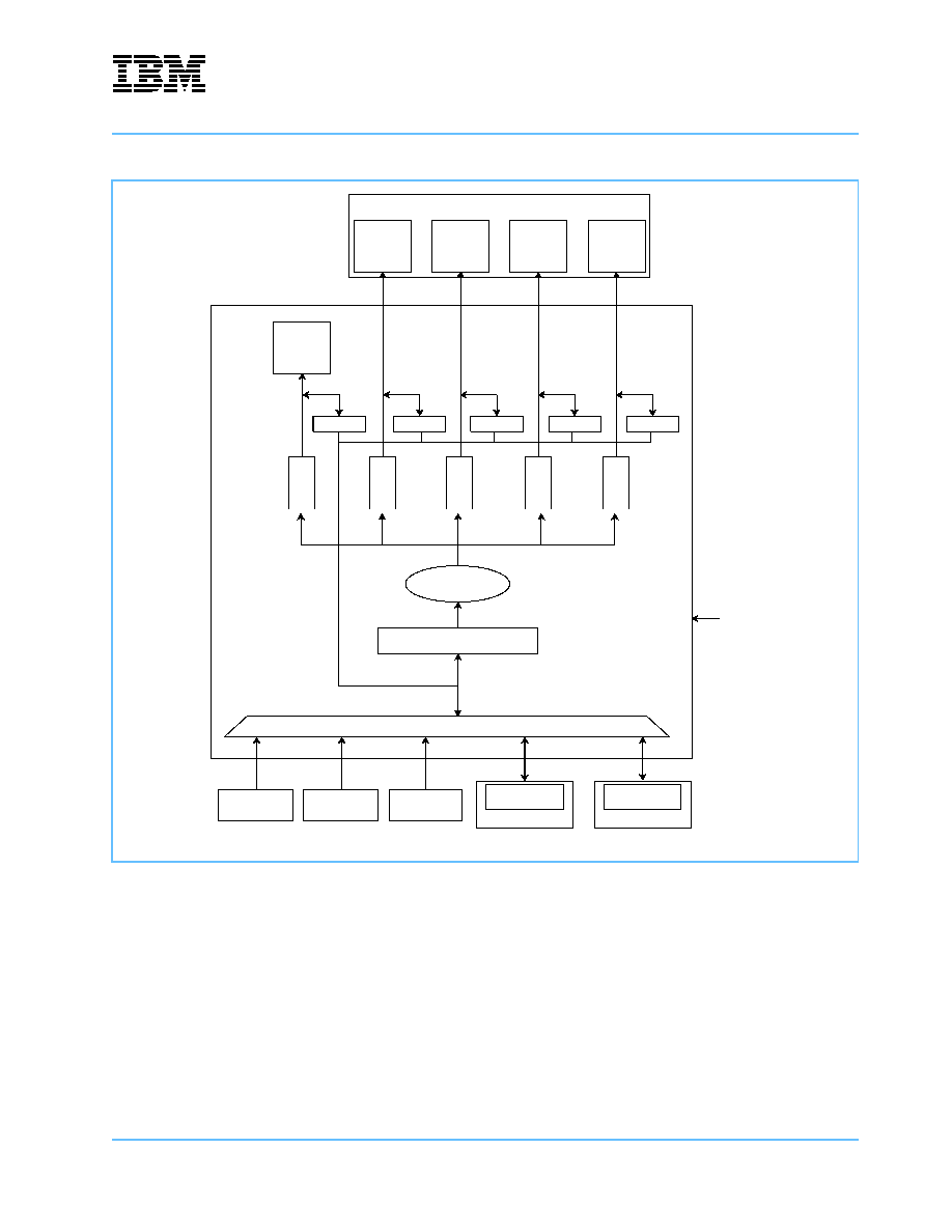
IBM PowerNP NP4GS3
Preliminary
Network Processor
np3_ds_sec07_EPC.fm.11
January 29, 2003
Embedded Processor Complex
Page 301 of 605
Figure 7-20. Counter Manager Block Diagram
Ingress
Flow Control
Internal
Counter
DRAM
Bank
CntrQ4
CntrQ0
CntrQ1
Address &
Update Value
Counter Definition Table
Multiplexer / Arbitration
DPPU7
Counter
Coprocessor
DPPU0
CntrQ2
CntrQ3
Read
Read
Read
Read
Read
...
Policy
External DRAM - D2
A
DRAM
Bank
B
DRAM
Bank
C
DRAM
Bank
D
Manager
Counter
Manager
Counter
Coprocessor
Memory
Egress
Flow Control

IBM PowerNP NP4GS3
Network Processor
Preliminary
Embedded Processor Complex
Page 302 of 605
np3_ds_sec07_EPC.fm.11
January 29, 2003
7.9.1 Counter Manager Usage
The Counter Manager manages various counters for the EPC. The EPC, Policy Manager, and the Ingress
and Egress Flow Control have the ability to update these counters. The picocode accesses these counters for
statistics, flow control actions, and policy decisions. Before a counter can be used, its counter definition entry
must be configured. This entry defines where the counter is stored, how many counters are associated with
this set, and the counter's size. The Counter Manager supports 256 different counter definition entries. The
counter definition entry is written to the Counter Definition Table using the CAB. The entry format in shown in
Table 7-97 on page 303.
Table 7-94. Counter Manager Components
Component Name
Description
Counter Definition Table
Contains definitions for each counter block (256 entries). A counter block is made up of the counter's
memory storage location (Bank A, Bank B, Bank C, Bank D, or Internal), the base address within that
memory, the number of counters within the set, and the counter size.
Multiplexing and Arbitration
Multiplexing and arbitration logic selects the next counter action from all requestors according to prior-
ity. Flow Control has the highest priority, Policy Manager the next, and the set of DPPUs the lowest pri-
ority. Multiplexing and arbitration logic uses two work conserving round-robins: one between the two
Flow Control requestors and one for the set of DPPUs. This logic returns the read data to the appropri-
ate requestor during counter reads.
Address and Update Value
Address and Update Value logic uses information gathered from the Counter Definition Table and the
parameters passed from the requestor to create the final counter address and update value.
CntrQ0 - CntrQ4
Five Counter Queues used to temporarily hold the counter request and allow the Counter Manager to
access all five memory locations independently. The request is placed into the appropriate queue
based on the memory storage location information found in the Counter Definition Table.
Read
Read logic gathers the read data from the appropriate memory location and returns it to the requestor.
Internal Counter Memory
Internal Counter Memory holds the "fast" internal counters and can be configured to hold 64-bit, 24/40-
bit, or 32-bit counters. The Internal Counter Memory size is 1024 locations x 64 bits.
Table 7-95. Counter Types
Type Name
Description
64-bit Counter
Counter that holds up to a 64-bit value.
24/40-bit Counter
Special 64-bit counter that has a standard 40-bit portion and a special 24-bit increment portion. The 40-
bit portion is acted upon by the command passed and the 24-bit portion is incremented. This counter
allows "byte count" and "frame count" counters to be in one location; the 40-bit portion is the byte
count, and the 24-bit portion is the frame count.
32-bit Counter
Counter that holds up to a 32-bit value.
Table 7-96. Counter Actions
Action Name
Description
Read
Read Counter and return value (either 64 or 32 bits) to the EPC.
Read/Clear
Read Counter and return value (either 64 or 32 bits) to the EPC. Hardware then writes counter to zero.
Write
Write 16 bits to the counter (either bits 31:16 or 15:0) and zero all other bits.
Increment
Add one to the counter value and store updated value in memory.
Add
Add 16 bits to the counter value and store updated value in memory.

IBM PowerNP NP4GS3
Preliminary
Network Processor
np3_ds_sec07_EPC.fm.11
January 29, 2003
Embedded Processor Complex
Page 303 of 605
The Counter Definition Entry describes a set of counters that have similar characteristics and are referenced
from the picocode as a single group. Figure 7-21 on page 304 shows several counter definition examples.
Table 7-97. Counter Definition Entry Format
Field
Bits
Definition
Reserved
31:30
Not used.
24/40
29
Flag to indicate 24/40 counter (1 = 24/40). If set, 64 / 32 must also be set to 1.
64 / 32
28
Flag to indicate a 64-bit counter (1 = 64) or a 32-bit counter (0 = 32).
Number of Counters
27:23
Number of counters within this counter set. Legal values:
1, 2, 4, 8, or 16
Counter Resource Location
22:20
Storage used for the counter block.
000
Bank A
001
Bank B
010
Bank C
011
Bank D
100
Internal Memory
Base Address
19:0
Base Address within the memory where the counter block starts.
Counter addresses are based on a 64-bit word, however, all address bits are
not used for all counter resource locations and when a 32-bit counter is indi-
cated (bit 28 is set to 0), address bit 0 indicates the counter location within the
64-bit word (0 = bits 31:0, 1 = bits 63:32). The following illustrates the use of
the base address bits.
32-bit
Counter Resource
64-bit word
counter
Location
address
----------
-------------------------
--------------
Yes
'000' - '011'
19:1
Yes
'100'
11:1
No
'000' - '011'
19:0
No
'100'
10:0

IBM PowerNP NP4GS3
Network Processor
Preliminary
Embedded Processor Complex
Page 304 of 605
np3_ds_sec07_EPC.fm.11
January 29, 2003
Each Counter Definition Entry can be used for a block of counter sets. The definition describes one counter
set and the picocode can reference several consecutive counter sets using the same definition. For example,
a counter set is defined as four counters: one for frames less than 500 bytes, one for frames between 500
and 1000 bytes, one for frames between 1001 and 1518 bytes, and the last one for frames greater than 1518.
One Counter Definition Entry describes the counters, and picocode can use the definition to reference 40
similar sets of these counters, that is, one for each source port. Counter Set 0 is located at the Base Address
defined by the entry, Counter Set 1 is located at the next available address, and so on. Figure 7-22 on page
305 shows an example of counter blocks and sets.
Figure 7-21. Counter Definition Entry
Counter Definition Entry 3
Counter Definition Entry 8
Counter Definition Entry 45
Number of Counters in set = 4
Counter Resource = Bank A
Base Address = x`0 1004'
Number of Counters in set = 8
Counter Resource = Bank C
Base Address = x`0 1608'
Number of Counters in set = 2
Counter Resource = Internal
Base Address = x`0 0044'
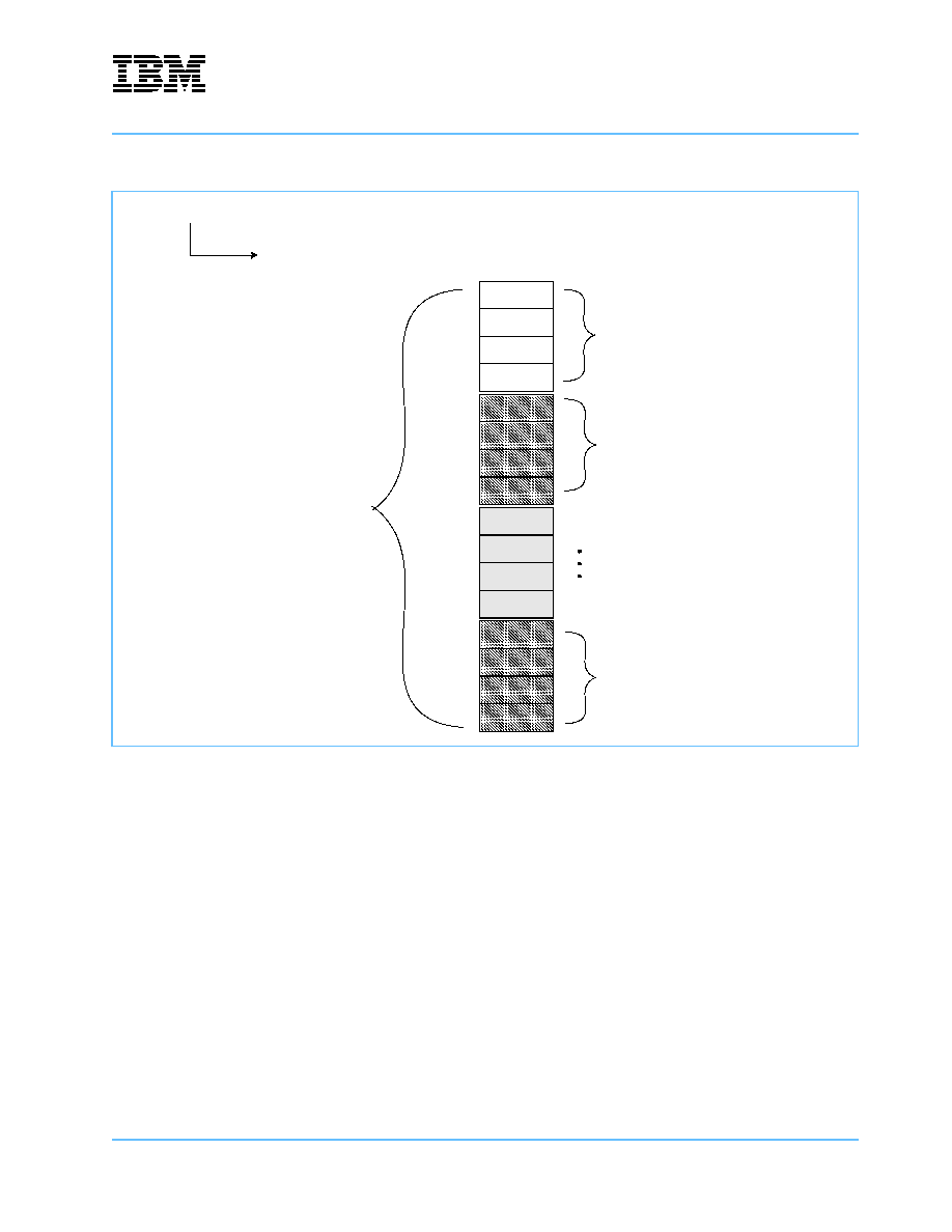
IBM PowerNP NP4GS3
Preliminary
Network Processor
np3_ds_sec07_EPC.fm.11
January 29, 2003
Embedded Processor Complex
Page 305 of 605
To reference the correct counter, the requestor must pass the Counter Manager several parameters. These
parameters are described inTable 7-98 on page 306.
Figure 7-22. Counter Blocks and Sets
Counter Definition Entry 3
Number of Counters in set = 4
Counter Resource = Bank A
Base Address = x`0 1004'
Counter Set 0
Counter Set 1
Counter Set 39
< 500
500 - 1000
1001 - 1518
> 1518
Counter Block 3

IBM PowerNP NP4GS3
Network Processor
Preliminary
Embedded Processor Complex
Page 306 of 605
np3_ds_sec07_EPC.fm.11
January 29, 2003
The Counter Manager builds the actual counter address using the following algorithm:
Address = Base Address + (Counter Set Index * Number of Counters) + Counter Number
This address is used to access the counter within the appropriate memory (Bank A, Bank B, Bank C, Bank D,
or Internal). When a 32-bit counter is accessed, the low order bit of the address selects which 32 bits of the
64-bit memory word are being used: 0 = bits 31:0, 1 = bits 63:32.
The location of the counter and its size determine how many address bits are used by the Counter Manager
as seen in Table 7-99.
Table 7-98. Counter Manager Passed Parameters
Parameter
Bits
Definition
Counter Definition Table Index
8
Counter Definition Entry to use for this action
Counter Set Index
20
Set of counters to reference
Counter Number
4
Counter within the set to reference
Action
3
Action to perform on the counter
Modify
000
Increment by 1
001
Add 16 bits to counter
Read
100
Standard read
101
Read then Clear value
Write
110
Write bits 15:0 of counter; all other counter bits are set to zero
111
Write bits 31:16 of counter; all other counter bits are set to
zero
All other code points are reserved.
Add/Write Value
16
Value to add to counter when Modify/Add selected
Value to write to counter when Write selected
Flow Control Action
(Counter Definition Table Index Offset)
2
Only used by Flow Control Interfaces
00 Standard
Enqueue
01
Discard (resulting from the Transmit Probability table)
10
Tail Drop Discard
11
Reserved
Table 7-99. Counter Manager use of Address Bits
Memory Location
Counter Size
Number of Counters
stored at Single Memory
Address
Number of Address bits used
Total Counters Possible
Internal
32
2
11
(10:0) where bit 0 selects
upper or lower 32 bits
1K loc * 2 per =
2K
64, 24/40
1
10
(9:0)
1K loc * 1 per =
1K
DRAM Banks
(A, B, C, or D)
32
2
20
(19:0) where bit 0 selects
upper or lower 32 bits
512K loc * 2 per * 4 banks =
4M
64, 24/40
1
20
(19:0)
1M loc * 1 per * 4 banks =
4M

IBM PowerNP NP4GS3
Preliminary
Network Processor
np3_ds_sec07_EPC.fm.11
January 29, 2003
Embedded Processor Complex
Page 307 of 605
The Counter Manager supports a special mode of operation when used by the Ingress or Egress Flow
Control. This mode allows "delayed increments" to occur based on flow control information. Both Flow
Controls pass an additional parameter, Flow Control Action, that causes the Counter Manager to modify
which Counter Definition Entry is used. A standard enqueue sent by either Flow Control logic causes the
Counter Manager to use the Counter Definition Index that is passed with the request. A discard resulting from
the Transmit Probability table causes the Counter Manager to access the Counter Definition Entry that is
located at Index+1. A Tail Drop Discard causes the Counter Manager to access the Counter Definition Entry
located at Index+2. Each type of flow control action uses a different counter definition.
When the Policy Manager requests use of the Counter Manager, it always uses a Counter Definition Table
Index of 0. This location is reserved for use by the Policy Manager.
The Counter Manager arbitrates for a new counter action at a rate of one each 15 ns. When accessing the
internal memory, the Counter Manager can update these counters at a rate of one every 15 ns. The external
DRAM rates are once each 150 ns or each 165 ns depending on DRAM cycle configuration (10- or 11-cycle
windows), and one to four counters (one per bank) will be updated during this time. If the Counter Manager is
updating some (but not all) DRAM banks, the banks not being updated by the Counter Manager will have
their last location (address = all 1's) written during the DRAM write window. Therefore, the last location of
each DRAM bank must be reserved for this use and cannot be assigned as a counter location.
The Counter Manager supports the following actions: read, read/clear, write/lower, write/upper, increment
and add. The DPPUs can read any counter in the Counter Manager. The Flow Control and Policy Manager
logic do not perform counter reads. When a counter is read, the Counter Manager returns the read data
(either 32 or 64 bits) with the acknowledge signal. The picocode can also clear the counter (set to zero) after
the read is performed by passing the Read/Clear action. Counter writes of 16 bits are supported and either
bits 15:0 or bits 31:16 of the selected counter are set to the write value with all other bits set to zero (this
feature is provided to assist in chaining unused counters into a free list).
The Counter Manager also supports incrementing or adding to the selected counter. The add value can be up
to 16 bits in size and will be added to the counter (either 32, 40, or 64 bits). When a 24/40 counter is incre-
mented or added, the 24-bit portion of the counter is incremented and the 40-bit portion receives the incre-
ment/add action.
The Counter Manager supports the following maximum numbers of counters (actual number depends on size
of DRAM used and the Counter Definition Table information):
� Up to 1 K 64-bit, or 2 K 32-bit Internal Counters, or some mix of 64 and 32-bit counters not to exceed
64 Kb total size.
� Up to 1 M 64-bit, or 1 M 32-bit External Counters per DRAM Bank, or some mix of 64- and 32-bit counters
not to exceed 1 M total counters per bank.

IBM PowerNP NP4GS3
Network Processor
Preliminary
Embedded Processor Complex
Page 308 of 605
np3_ds_sec07_EPC.fm.11
January 29, 2003
7.10 Semaphore Manager
The semaphore manager is located within the EPC and is controlled by a thread through a semaphore copro-
cessor.
A semaphore is a mechanism for acquiring ownership or "locking down" an entity. A semaphore is a 32-bit
value. Once a thread has exclusive ownership of a semaphore, it is guaranteed that there are no other
threads that own a semaphore with the same value (though there may be other threads owning semaphores
with different values). Thus, other threads that also want ownership of a semaphore with the same value are
blocked until the semaphore is unlocked.
It is upon the programmer to attach a meaning to a semaphore. That is, the semaphore manager does not
know what a semaphore represents - it is just a string of 32 bits. Semaphores can be seen as having a 32-bit
address space and the programmer can map this to anything, for example, the Tree Search Memory, the
data store, or the Embedded PowerPC. For example, a tree search memory can have the upper four bits of
the semaphore value set to `0000', an ingress data store address can have the upper four bits of the sema-
phore value set to `0001', and the embedded PowerPC mailbox may have the upper four bits set to `1111'.
In NP4GS3B (R2.0), when configured for ordered semaphores, a thread may have only one semaphore
locked at a time. When the NP4GS3B (R2.0) is configured for unordered semaphores only, then a thread
may have two semaphores (unordered) locked at a time. In NP4GS3C (R3.x), when configured for ordered
semaphores, a thread can have two semaphores locked at a time, but only one of them can be ordered.
� Unordered Semaphores - When multiple threads request a semaphore, the semaphore manager will
grant the request through a round-robin fairness algorithm. A thread can lock-and-unlock an unordered
semaphore as often as it wants. For example, it can lock-and-unlock, execute some code, lock again, exe-
cute more code, unlock, etc.
� Ordered Semaphores - When multiple threads request a semaphore, the semaphore manager will grant
the request in the order of frame dispatch for a given flow. In other words, when a thread is processing a
frame of a certain flow that has been dispatched before any other frames of the same flow, then it is guar-
anteed by the semaphore manager that this thread will get a certain semaphore value before any other
threads that are processing frames of the same flow. The dispatch order will be maintained by placing a
"reservation" into a queue. Only semaphore requests in which their reservation is on the top of the queue
will be serviced. It will be the responsibility of the picocode to release a reservation if it isn't needed or a
deadlock situation will occur.
To use ordered semaphores, they must be enabled. This is done by writing the ordered semaphore enable
register in the hardware classifier. There is one bit for the semaphore 0 ID queue, and one bit for the sema-
phore 1 ID queue. At dispatch time, the hardware classifier may assign a Completion Unit label to a frame as
per the Port Configuration table.
1
If a Completion Unit label is assigned, the hardware classifier will examine
the ordered semaphore enable register to see if ordered semaphores are enabled as well. If Completion Unit
label generation is not enabled, ordered semaphores will not be enabled for this dispatch. The Completion
Unit and the semaphore ordering queues use the same label. If a Completion Unit label is released (via an
enqueue with label or release label command), the semaphore order label must first have either been used or
released, otherwise an error will occur.
1. When the CULabGenEnabled field of the Port Configuration Table (see Table 7-82 on page 286) is set to `1'.

IBM PowerNP NP4GS3
Preliminary
Network Processor
np3_ds_sec07_EPC.fm.11
January 29, 2003
Embedded Processor Complex
Page 309 of 605
A thread can lock-and-unlock an ordered semaphore up to two times. During a request, the thread must
specify the OrderID, which is 0 or 1. An order queue can only be used once, with two order queues imple-
mented for a total of two ordered semaphores per thread. In other words, a thread can only lock OrderID 0
once, and OrderID 1 once.
Each thread can have ownership of up to two semaphores simultaneously. When using two semaphores, the
programmer must take great care to avoid deadlock situations (semaphores can only be requested one by
one). For example, a semaphore lock must be followed at some point by a semaphore unlock or a deadlock
will occur.
The semaphore manager employs a pending concept to ordered semaphore lock requests, which enables it
to look past the head of the completion unit queues. The basic idea is if a thread is requesting an ordered lock
for a particular semaphore value that is already locked, it will be moved into a pending state, and it's request
will not be considered complete. At this point, the threads that are behind it in the flow queues can now be
considered for locking as long as their semaphore values are different. Once the original semaphore value
that was locked is unlocked, then the pending thread's semaphore value will lock and that thread's request
will be completed. It is important to note that only one thread per semaphore value will go into the pending
state.
The semaphore manager will process the three semaphore coprocessor command types in parallel:
� Lock commands for ordered semaphores at the head of the queue and lock commands for unordered
semaphores will be evaluated at the same priority level and a winner will be chosen using a round-robin
fairness algorithm.
- Lock commands will be evaluated in parallel with Unlock and Reservation Release commands.
� Unlock commands
- Unlock commands will be evaluated in parallel with Lock and Reservation Release commands.
� Reservation Release commands
- Reservation Release commands will be evaluated in parallel with Lock and Unlock commands.

IBM PowerNP NP4GS3
Network Processor
Preliminary
Embedded Processor Complex
Page 310 of 605
np3_ds_sec07_EPC.fm.11
January 29, 2003

IBM PowerNP NP4GS3
Preliminary
Network Processor
np3_ds_sec08_tree.fm.11
January 29, 2003
Tree Search Engine
Page 311 of 605
8. Tree Search Engine
8.1 Overview
The Tree Search Engine (TSE) is a hardware assist that performs table searches. Tables in the network
processor are maintained as Patricia trees, with the termination of a search resulting in the address of a leaf
page. The format of a leaf page or object is defined by the picocode; the object is placed into a control store,
either internal (H0, H1) or external (Z0, D0�D3).
8.1.1 Addressing Control Store (CS)
References to the control store use a a 26-bit address as shown in Table 8-1. Each address contains a
memory ID, a bank number, and address offset.
Table 8-2 provides addressing information and recommended uses for each memory that is supported by the
CSA and that is accessible via the TSE. The memory type provides access width and memory size informa-
tion. Selection for D0 as either single or double wide is by configuration (13.1.2 DRAM Parameter Register
(DRAM_Parm) on page 462).
Table 8-1. Control Store Address Mapping for TSE References
26-bit Address Used to Reference the Control Store
4 bits
2 bits
20 bits
Memory ID
Bank Number
Offset
Virtual Bank Address
Table 8-2. CS Address Map and Use
(Page 1 of 2)
Memory ID
Bank No.
Memory Name
Type
Offset Width
(bits)
Recommended Use
0000
00
Null
20
01-11
Reserved
0001
00
Z0
External ZBT SRAM
512K x 36 (R2.0)
1M x 36 (R3.x)
19 (R2.0)
20 (R3.x)
Fast PSCB
01-11
Reserved
0010
00
H0
Internal SRAM
2K x 128
11
Fast Leaf pages
01
H1
Internal SRAM
2K x 36
11
Fast internal SRAM
10
Reserved
11
Reserved
0011
00-11
Reserved
0100�0111
00-11
Reserved

IBM PowerNP NP4GS3
Network Processor
Preliminary
Tree Search Engine
Page 312 of 605
np3_ds_sec08_tree.fm.11
January 29, 2003
8.1.2 D6 Control Store.
The NP4GS3 supports the following DDR DRAM types for the D6 control store:
The D6 control store can be accessed either via the TSE or by the embedded PowerPC's Processor Local
Bus (PLB) (see 10.2 Processor Local Bus and Device Control Register Buses on page 389).
8.1.3 Logical Memory Views of D6
Using the PLB, the embedded PowerPC or a PCI attached host views a flat, contiguous address space
addressable on byte boundaries.
Access via the TSE uses the Control Store address mapping described in 8.1.1 Addressing Control Store
(CS) on page 311, and is composed of a Memory ID, Bank Number and offset. The offset limits addressing
capability to 8-byte boundaries within the DDR DRAM.
Table 8-3 illustrates the PLB to D6 control store address translation. The PLB address is shown within the
body of the table and the D6 control store address is formed using the Memory ID, Bank Number, and Offset.
1000
00-11
D0 banks A-D
DDR DRAM
D0_Width = 0
8 MB
16 MB
32 MB
D0_Width = 1
16 MB
32 MB
64MB
18-20
Single (D0_width = 0) or double wide
(D0_width = 1) configuration. Leaf
Pages
1001
00-11
D1 banks A-D
DDR DRAM
8 MB
16 MB
32 MB
18-20
Leaf Pages
1010
00-11
D2 banks A-D
Leaf or Counter pages
1011
00-11
D3 banks A-D
DT entries and PSCB entries
1100
00-11
D6 banks A-D
DDR DRAM
8 MB
16 MB
32 MB
64MB
128 MB
20
PowerPC external memory
1101
1110
1111
Note: DDR DRAM is specified as: Number of banks
� number of entries � burst access width (in bits).
DDR DRAM
Total Memory Space (MB)
4 x 1M x 16
� 1 chip
8
4 x 2M x 16
� 1 chip
16
4 x 4M x 4
� 4 chips
32
4 x 4M x 16
� 1 chip
32
4 x 8M x 4
� 4 chips
64
4 x 16M x 4
� 4 chips
128
Table 8-2. CS Address Map and Use
(Page 2 of 2)
Memory ID
Bank No.
Memory Name
Type
Offset Width
(bits)
Recommended Use

IBM PowerNP NP4GS3
Preliminary
Network Processor
np3_ds_sec08_tree.fm.11
January 29, 2003
Tree Search Engine
Page 313 of 605
D6 control stores implemented in DDR DRAM of up to 32 MB in size are accessed by the TSE using only
Memory ID '1100'. Larger D6 control stores require Memory IDs of '1101' (up to 64 MB), '1110' (up to 96 MB)
and '1111' (up to 128 MB).
A method to share memory objects between the embedded PowerPC or attached PCI host using the PLB,
and picocode running on the NP4GS3 using TSE instructions is to specify the object (as viewed by the TSE)
with a height of one and a width of four. This allows the TSE access to all of the D6 control store, on 32-byte
boundaries, and is consistent with the PLB's flat contiguous address space view. Successive objects with a
height of one and a width of four are accessed by incrementing the TSE address until a 32MB boundary is
reached. At the boundary it is necessary to increment the Memory ID to address the next successive object.
8.1.4 Control Store Use Restrictions
The following restrictions apply:
� When D2 is used by the counter manager, the last location (highest address) in each bank must not be
assigned for any use.
� DT entries can be stored only in H1, Z0, or D3.
� PSCBs can be stored only in H1, Z0, or D3.
� Leaf pages can be stored only in H0, D0, D1, and D2.
Table 8-3. PLB and D6 Control Store Addressing
Memory ID
(4 bits)
Bank A (`00')
Bank B (`01')
Bank C (`10')
Bank C (`11')
Offset
(20 bits)
`1100'
0-7
8-x`F
x`10-x`17
x`18 - x`1F
x`00 0000'
x`20-x`27
x`28-x`2F
x`30-x`37
x`38-x`3F
x`00 0001'
x`07F FFE0 -
x`07F FFE7
x`07F FFE8 -
x`07F FFEF
x`07F FFF0 -
x`07F FFF7
x`07F FFF8 -
x`07F FFFF (8MB-1)
x`03 FFFF'
x`0FF FFE0 -
x`0FF FFE7
x`0FF FFE8 -
x`0FF FFEF
x`0FF FFF0 -
x`0FF FFF7
x`0FF FFF8 -
x`0FF FFFF (16MB-1)
x`07 FFFF'
x`1FF FFE0 -
x`1FF FFE7
x`1FF FFE8 -
x`1FF FFEF
x`1FF FFF0 -
x`1FF FFF7
x`1FF FFF8 -
x`1FF FFFF (32MB-1)
x`0F FFFF'
'1101'
x`200 0000 -
x`200 0007
x`200 0008 -
x`200 000F
x`200 0010 -
x`200 0017
x`200 0018 -
x`200 001F
x`00 0000'
x`3FF FFE0 -
x`3FF FFE7
x`3FF FFE8 -
x`3FF FFEF
x`2FF FFF0 -
x`2FF FFF7
x`3FF FFF8 -
x`3FF FFFF (64MB-1)
x`0F FFFF'
x`400 0000 -
x`400 0007
x`400 0008 -
x`400 000F
x`400 0010 -
x`400 0017
x`400 0018 -
x`400 001F
x`00 0000'
x`5FF FFE0 -
x`5FF FFE7
x`5FF FFE8 -
x`5FF FFEF
x`5FF FFF0 -
x`5FF FFF7
x`5FF FFF8 -
x`5FF FFFF (96MB-1)
x`0F FFFF'
'1111'
x`600 0000 -
x`600 0007
x`600 0008 -
x`600 000F
x`600 0010 -
x`600 0017
x`600 0018 -
x`600 001F
x`00 0000'
x`7FF FFE0 -
x`7FF FFE7
x`7FF FFE8 -
x`7FF FFEF
x`7FF FFF0 -
x`7FF FFF7
x`7FF FFF8 -
x`7FF FFFF (128MB-1)
x`0F FFFF'

IBM PowerNP NP4GS3
Network Processor
Preliminary
Tree Search Engine
Page 314 of 605
np3_ds_sec08_tree.fm.11
January 29, 2003
8.1.5 Object Shapes
Object shapes specify how the control store stores an object such as a leaf or pattern search control block
(PSCB). A leaf is a control block that contains the reference key as a reference pattern. The pattern uniquely
identifies the leaf in a tree and contains the data needed by the application initiating a tree search. The data is
application-dependent, and its size or memory requirements are defined by the LUDefTable entry for the tree.
See Table 8-5: Height, Width, and Offset Restrictions for TSE Objects on page 316 and
Table 8-17. LUDefTable Entry Definitions on page 333 for details.
Shape is defined by two parameters, height and width. Objects small enough to fit within a single memory or
bank location are defined as having a height and width of 1 (denoted by 1,1), and therefore do not require
shaping. For example, both a 32-bit and a 48-bit object stored in a DDR SDRAM bank would have a shape of
(1,1).
When objects do not fit into a single memory or bank location, they have heights and/or widths > 1:
� Height denotes the number of consecutive address locations in which an object is stored. For example, if
the height of an object = 4 and the control store address = A, the object is stored in locations A, A+1, A+2,
and A+3.
� Width denotes the number of consecutive banks in which the object is stored. Width always = 1 for
objects stored in ZBT SRAM, and could be > 1 for objects in DDR SDRAM. For example, if the width of an
object = 3, and its height = 1, the object is stored in three consecutive banks (the virtual bank address is
incremented by 1).
� An offset increment can carry out into the bank address bits. This is not a supported use of the CS mem-
ory, and table allocation algorithms must be defined to avoid this condition.
� For height and width, the hardware automatically reads the appropriate number of locations. From a pico-
code point of view, an object is an atomic unit of access. For the accesses with height or width of more
one, other requesters are not blocked. Restrictions to height, width, and offset are given in Table 8-5:
Height, Width, and Offset Restrictions for TSE Objects on page 316. Table 8-17: LUDefTable Entry Defini-
tions on page 333 specifies the leaf and PSCB shapes.
Figure 8-1. Example Shaping Dimensions on page 315 illustrates some example placement of objects with
different shapes in control store. An object may span more than one DRAM as shown in examples (b) and (c)
with the following restrictions:
� An object may span D1 and D2.
� When D0 is configured as a single wide (D0_Width = 0), then an object may span D0 and D1.
� Objects may not span out of D0 when D0 is configured as a double wide (D0_Width = 1).
� Objects may not span into or out of Z0, H0, H1, D3 or D6.
� Shape object can define a maximum of 512 bits for any memory.
Table 8-4. DTEntry, PSCB, and Leaf Shaping
Object
Shape
FM DTEntry/PSCB
Always has a shape of height = 1, width = 1.
SMT DTEntry/PSCB
Always has a shape of height = 1, width = 1.
LPM DTEntry/PSCB
Has a shape of height = 1, width = 1 or height = 2, width = 1 depending on the memory in which the PSCB
resides. A memory with a line width of at least 64 bits should be used with height = 1 and a memory of 36
bits should be used with height = 2.
Leaf
Can have any shape that is allowed by the memory in which the leaf is located - maximum of 512 bits.

IBM PowerNP NP4GS3
Preliminary
Network Processor
np3_ds_sec08_tree.fm.11
January 29, 2003
Tree Search Engine
Page 315 of 605
Figure 8-1. Example Shaping Dimensions
(2,1)
(3,1)
128
H0
H = 1, W = 1
H = 5, W = 1
(Note: 4 bits
unused)
32
Z0
H = 1, W = 1
36
D1
(Height = 1,Width = 4)
64
D2
(1,2)
(3,1)
64
64
64
(Height = 1,Width = 3)
D1
(Height = 1,Width = 4)
D2
(3,1)
(Height = 1,Width = 3)
(1,1)
(1,1)
(1,1)
a
b
c
d
a
b
c
d
a
b
c
d
a
b
c
d
64
64
64
64
64
64
64
64
64
64
64
64
H = 3, W = 1
Example (a)
Example (b)
Example (c)

IBM PowerNP NP4GS3
Network Processor
Preliminary
Tree Search Engine
Page 316 of 605
np3_ds_sec08_tree.fm.11
January 29, 2003
8.1.6 Illegal Memory Access
When the TSE uses an undefined MemoryID (that is, reserved) or an illegal memory shape, the TSE aborts
the current command, returns a KO status, and sets an exception flag at bit 2 in interrupt class 3
(TSM_Illegal_Memory_Access). The exception flag can be set to cause an interrupt by setting bit 2 of inter-
rupt mask 3 to `1' (TSM_Illegal_Memory_Access). For debugging purposes, an exception can switch a
programmable set of threads into single-step mode.
Table 8-5. Height, Width, and Offset Restrictions for TSE Objects
Memory
Height
Width
Total Object Size (bits)
Control Store Address
Offset
Must Be Divisible By
H0
1
2
3
4
1
1
1
1
128
256
384
512
1
2
4
4
H1
1
2
3
4
5
6
7
8
1
1
1
1
1
1
1
1
36
64
96
128
160
192
224
256
1
2
4
4
8
8
8
8
Z0
1
2
3
4
5
6
7
8
1
1
1
1
1
1
1
1
36
64
96
128
160
192
224
256
1
2
4
4
8
8
8
8
D0
(D0_Width = 1; double
wide configuration)
1
2
3
4
1
2
1
1
1
1
1
1
2
2
3
4
128
256
384
512
256
512
384
512
1
2
4
4
1
2
1
1
D0-D1-D2-D3-D6
(D0_Width = 0; single
wide configuration)
1
2
3
4
5
6
7
8
1
2
3
4
1
2
1
2
1
1
1
1
1
1
1
1
2
2
2
2
3
3
4
4
64
128
192
256
320
384
448
512
128
256
384
512
192
384
256
512
1
2
4
4
8
8
8
8
1
2
4
4
1
2
1
2

IBM PowerNP NP4GS3
Preliminary
Network Processor
np3_ds_sec08_tree.fm.11
January 29, 2003
Tree Search Engine
Page 317 of 605
8.1.7 Memory Range Checking (Address Bounds Check)
Memory range checking can flag access to a programmable range within Min_addr_Bounds and
Max_addr_Bounds for read, write or both using Addr_Bounds_Cntl. Min_addr_Bounds. Memory range
checking can be performed for any TSE Control Store accesses only. When memory range checking is
enabled, any Control Store read, write, or read/write address falling within or at the boundary of the defined
range, generates an exception (an exception does not stop TSE operation) and sets an exception flag at bit 1
in interrupt class 3 (TSM_Addr_Range_Violation). The exception flag can be set to cause an interrupt by
setting bit 1 of interrupt mask 3 to `1' (TSM_Addr_Range_violation). For debug purpose, Bounds Violation
Register (Bounds_vio), indicates which GxH has caused an address bounds exception.

IBM PowerNP NP4GS3
Network Processor
Preliminary
Tree Search Engine
Page 318 of 605
np3_ds_sec08_tree.fm.11
January 29, 2003
8.2 Trees and Tree Searches
The TSE uses trees to store and retrieve information. Tree searches, retrievals, inserts and deletes are
performed according to a key that is similar to a MAC source address or a concatenation of an IP source and
destination address. Information is stored in one or more leaves that contain the key as a reference pattern
and, typically, contain aging and user information for forwarding purposes such as target blade and target
port numbers.
To locate a leaf, a search algorithm processes input parameters that include the key and hashes the key. The
algorithm then accesses a direct table (DT) and walks the tree through the PSCBs. There are three types of
trees, each with its own search algorithm and tree-walk rules: full match (FM); longest prefix match (LPM);
and software managed (SMT).
The data structure of FM and LPM trees is the Patricia tree. When a leaf is found, the leaf is the only candi-
date that can match the input key. A "compare-at-end" operation compares the input key with a reference
pattern stored in the leaf to verify a match. Search results are "OK" when a match is found and "KO" in all
other cases.
The data structure of SMT trees is similar to that of FM trees, but SMT trees can have multiple leaves that can
be chained in a linked list. All leaves in the chain are checked against the input key until a match is found or
the chain is exhausted. Search results are "OK" when a match is found and "KO" in all other cases.
Table 8-6. FM and LPM Tree Fixed Leaf Formats
Field Name
Byte Length
Description
NLARope
4
Leaf chaining pointer, aging, and direct leaf information
Prefix_Len
1
Length of the pattern (in bits) for LPM only. Not used by TSE for FM trees and
can be used by picocode.
Pattern
2-24
Pattern to be compared with HashedKey. Always present. Length given by
P1P2_max_size from Table 8-17: LUDefTable Entry Definitions on page 333.
For FM: Unused bit between (p1p2_max_size - Hashedkey_length) must be ini-
tialize to zero.
For LPM: Unused bits between (p1p2_max_size - Prefix_Len), do not have to be
initialized and can be used by user data since these bits do not take part in com-
parsion.
UserData
Variable
Under picocode control. For example, field can include one or more counters.
Table 8-7. SMT Tree Fixed Leaf Formats
Field Name
Byte Length
Description
NLASMT
4
Leaf chaining pointer to chain leaves for SMT. Includes shape of chained leaf.
Comp_Table_Index
1
Defines index in CompDefTable that defines compare between Pattern1,
Pattern2, and HashedKey.
Pattern1 and Pattern2
4-48
Contains Pattern1 and Pattern2 bitwise interleaved (even bits represent Pattern1
and odd bits represent Pattern2). That is, bit 0 of the field contains bit 0 of
Pattern1, bit 1 contains bit 0 of pattern 2, etc.
Length given by 2*P1P2_Max_Size from Table 8-17: LUDefTable Entry Defini-
tions on page 333.
For SMT: Unused bit between (2 * p1p2_max_size - 2 * Hashedkey_length)
must be initialized to zero.
UserData
Variable
Under picocode control. For example, field can include one or more counters.

IBM PowerNP NP4GS3
Preliminary
Network Processor
np3_ds_sec08_tree.fm.11
January 29, 2003
Tree Search Engine
Page 319 of 605
8.2.1 Input Key and Color Register for FM and LPM Trees
For FM and LPM trees, the input key is hashed into a HashedKey according to the hash algorithm specified
by the Hash_type field in the LUDefTable. To minimize the depth of the tree that begins after the direct table,
the hash function output is always a 192-bit number with a one-to-one correspondence to the original input
key. Maximum output entropy is contained in the hash function's most significant bits. The N highest bits of
the HashedKey register are used to calculate an index into the direct table, where N is determined by the defi-
nition of the DT (Direct Table) entry for the tree.
When colors are enabled for a tree, the 16-bit color register is inserted after the input key has been hashed.
This occurs immediately after the direct table. If the direct table contains 2
N
entries, the 16-bit color value is
inserted at bit position N. The hash function output and the inserted color value (when enabled) are stored in
the HashedKey register. When colors are disabled, the 192-bit hash function is unmodified.
Colors can be used to share a single direct table among multiple independent trees. For example, color could
indicate a VLANID in a MAC source address table. The input key would be the MAC SA and the color the
VLANID (VLANID is 12 bits and 4 bits of the color would be unused, that is, set to 0). After the hash function,
the pattern would be 48 + 16, or 64 bits. The color would be part of the pattern to distinguish MAC addresses
of different VLANs.
8.2.2 Input Key and Color Register for SMT Trees
For SMT trees, the input key is a 192-bit pattern and the color register is ignored. No hashing is performed.
Table 8-8. Search Input Parameters
Parameter
Bit Length
Description
Key
192
Key must be stored in the Shared Memory Pool. All 192 bits must be set cor-
rectly (for Key Length shorter than 192, remaining bits in Shared Memory Pool
must be set to 0).
Key Length
8
Contains Key Length minus 1 in bits.
LUDefIndex
8
Index into LUDefTable that points to an entry containing a full definition of the
tree in which the search occurs. See Section 8.2.5.1 The LUDefTable on page
333.
TSEDPA
4
TSE Thread Shared Memory Pool Address - stores location of Key, KeyLength,
and Color and determines Leaf destination. The TSEDPA is the high order 4
bits of the thread's shared memory pool address (see 7.2.4 Shared Memory
Pool on page 196) and is constrained to be on a four-QW boundary. Use only
values of x`8', x`A', x`C', and x`E'.
LCBANr
1
Search results can be stored in either TSRx, as specified by TSEDPA. Leaf
addresses are stored in LCBA0 or LCBA1 as specified by LCBANr. During a
TSE search, picocode can access the other TSR to analyze the results of previ-
ous searches.
Color
16
For trees with color enabled, as specified in the LUDefTable, the contents of
the color register are inserted into the key during hash operation. See Section
8.2.1 Input Key and Color Register for FM and LPM Trees on page 319 for an
explanation of the process.
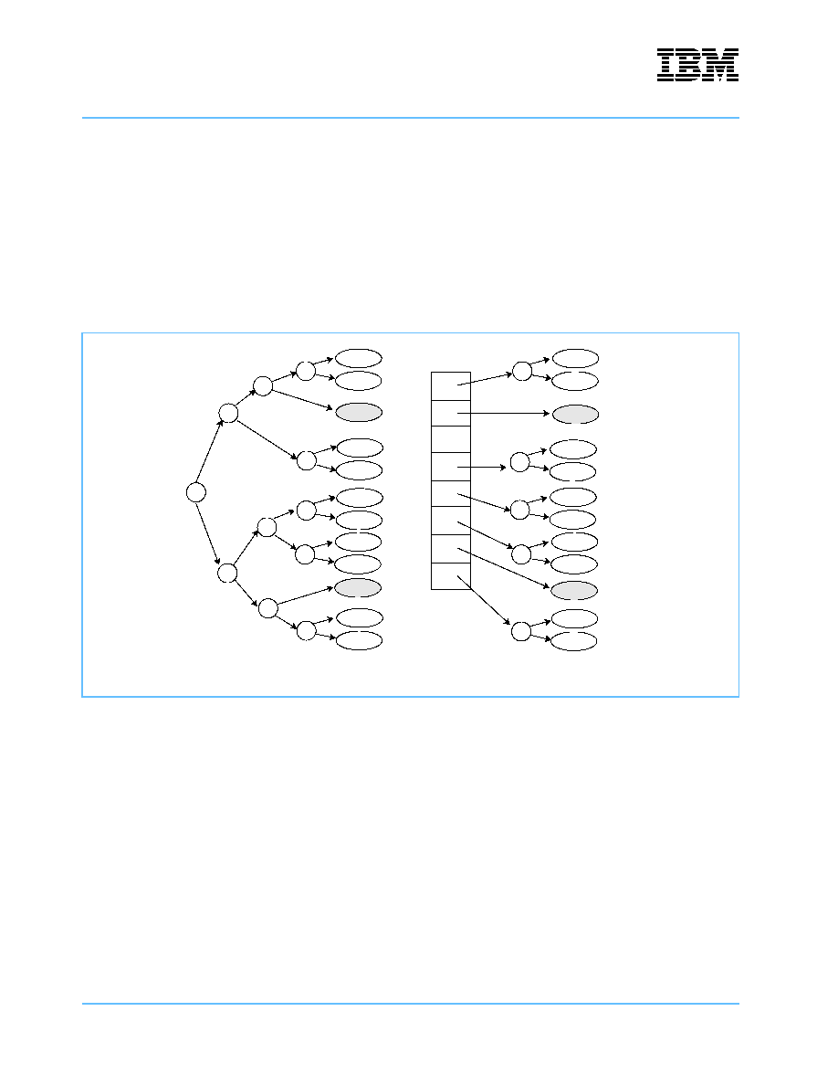
IBM PowerNP NP4GS3
Network Processor
Preliminary
Tree Search Engine
Page 320 of 605
np3_ds_sec08_tree.fm.11
January 29, 2003
8.2.3 Direct Table
A search starts when a DTEntry is read from the direct table. The read address is calculated from the N
highest bits of the HashedKey and from the tree properties defined in the LUDefTable. The DTEntry can be
represented as the root of a tree, with the actual tree data structure depending upon tree type. A Patricia tree
data structure is used with FM trees. Extensions to the Patricia tree are used with LPMs and SMTs. Using a
DT can reduce search time (PSCB access time). Increasing DT size is a trade-off between memory usage
and search performance. When a single leaf is attached to a DTEntry, the read data includes a pointer to the
leaf. When more than one leaf is attached, the read data defines the root of a tree. When the DTEntry is
empty, no leaf information is attached.
8.2.3.1 Pattern Search Control Blocks (PSCB)
A search begins when a DTEntry has been read if the DTEntry is neither empty nor contains a direct leaf. A
tree walk search starts at the DTEntry and passes one or more PSCBs until a leaf is found. For an FM tree,
the PSCB represents a node in the tree, or the starting point of two branches, "0" and "1". Each PSCB is
associated with a bit position "p" in the HashedKey. Bit p is the next bit to test (NBT) value stored in the
previous PSCB or in the DTEntry. Leaves reachable from a PSCB through the 0 branch have a `0' in bit p,
and leaves reachable through the 1 branch have a `1'. Leaves reachable through either branch have patterns
where bits 0..p-1 are identical, because pattern differences begin at bit p.
When an FM tree search encounters a PSCB, the TSE continues the tree walk on the 0 or 1 branch
depending on the value of bit p. Thus, PSCBs are only inserted in the tree at positions where leaf patterns
differ. This allows efficient search operations since the number of PSCBs, and thus the search performance,
depends on the number of leaves in a tree, not on the length of the patterns.
Figure 8-2. Effects of Using a Direct Table
Direct Table (DT)
Data structure without a Direct Table
Data structure with a Direct Table
Leaf
Leaf
Leaf
Leaf
Leaf
Leaf
Leaf
Leaf
Leaf
Leaf
Leaf
Leaf
Leaf
Leaf
Leaf
Leaf
Leaf
Leaf
Leaf
Leaf
Leaf
Leaf
Leaf
Leaf

IBM PowerNP NP4GS3
Preliminary
Network Processor
np3_ds_sec08_tree.fm.11
January 29, 2003
Tree Search Engine
Page 321 of 605
8.2.3.2 Leaves and Compare-at-End Operation
The entire HashedKey is stored in the leaf as a reference pattern, not as the original input key. During a tree
walk, only the HashedKey bits for which a PSCB exists are tested. When an FM leaf is found, its reference
pattern must be compared to the full HashedKey to make sure all the bits match. For SMT, if the leaf contains
a chain pointer or NLA field to another leaf, the new leaf's reference pattern is compared to the HashedKey.
Lacking a match or another NLA field, the search ends and the failure is indicated by a KO status. If the
pattern matches, the original input key is checked. If that matches, the whole leaf page is returned to the
network processor. If there is no match, the leaf page is returned with a no-match message.
8.2.3.3 Cascade/Cache
The direct table can be used as a cache to increase tree search performance since these trees are generally
small and contain most likely entries. During a search, the TSE first determines whether the DT contains a
pointer to a leaf matching the HashedKey. If so, the leaf is returned, eliminating the need for a search. To the
TSE, a cache lookup is identical to a normal search, that is, the input key is hashed into a HashedKey and the
DT is accessed.
Cascades/caches are enabled in the LUDefTable on a per-tree basis. If a cache search uses LUDefTable
entry I and the search ends with KO, another search using LUDefTable entry I+1 starts automatically. This
allows multiple search chaining, although the full tree should be stored under LUDefTable entry I+1. For
NP4GS3C (R3.x), cascading/caching of more than one LUDefTable entry is supported but the last Ludef-
Table entry must have the cache enable bit set to `0' (disabled).
For NP4GS3B (R2.0), Cascading/caching of more than one LUDefTable entry is not supported, therefore
LudefTable entry I+1 must have the cache enable bit set to `0' (disabled).
8.2.3.4 Cache Flag and NrPSCBs Registers
Picocode initiates insert and delete operations to and from the cache. Each search result stores information
about the cache in the CacheFlag and NrPSCBs registers as shown in Table 8-9. Each register is divided into
two sections, one for searches using TSE 0 coprocessor and the other for searches using TSE 1 copro-
cessor. There are two copies of these registers for each TSE 0 and TSE 1 resource. For NP4GS3C (R3.x),
CacheFlags represents the results for the first Cached Ludef entry when multiple search chaining is used.
Table 8-9. Cache Status Registers
Register
Bit Length
Description
CacheFlag(0)
1
CacheEmpty bit. Set when cache search finds an empty DTEntry in cache DT.
CacheFlag(1)
1
CacheLeafFound bit. Set when cache search finds a leaf and cache search returns OK. When
leaf found bit has been set, full search has not been performed.
CacheFlag(2)
1
CacheKO bit. Set when cache search returns KO. When cache is empty, this bit is also set.
NrPSCBs
8
After any search, contains the number of PSCBs read during a tree walk. When a cache
search finds no leaf and a full search starts, contains the number of PSCBs read during the
search.

IBM PowerNP NP4GS3
Network Processor
Preliminary
Tree Search Engine
Page 322 of 605
np3_ds_sec08_tree.fm.11
January 29, 2003
8.2.3.5 Cache Management
Cache management is performed using picocode. Cache inserts are controlled by inspecting the CacheFlag
and NrPSCBs registers after each tree search. Inserts are treated like normal FM tree inserts, allowing the
association of multiple leaves with a single DTEntry, because normal FM inserts create PSCBs to handle
multiple leaves. Inserts can also be done by writing directly to a DTEntry, although only using single leaves.
Cache deletes use the tree aging mechanism whereby every N seconds all entries in the cache are deleted.
8.2.3.6 Search Output
The output of a search operation consists of the parameters listed in Table 8-10.
8.2.4 Tree Search Algorithms
The TSE provides hardware search operations for FM, LPM, and SMT trees. Software initializes and main-
tains trees. Leaves can be inserted into and removed from FM and LPM trees without control point function
(CPF) intervention, permitting scalable configurations with CPF control when needed.
8.2.4.1 FM Trees
Full Match (FM) trees provide a mechanism to search tables with fixed size patterns, such as a Layer 2
Ethernet Unicast MAC tables which use fixed six-byte address patterns. Searches of FM trees are efficient
because FM trees benefit from hash functions. The TSE offers multiple fixed hash functions that provide very
low collision rates.
Each DTEntry is 36 bits wide and contains the formats listed in Table 8-11. PSCBs have the same structure
as DTEntrys except they contain two PSCBLines, each of which can have one of the two pointer formats
listed in this table: Next Pointer Address (NPA) or Leaf Control Block Address (LCBA). The two PSCBLines
are allocated consecutively in memory and are used as walking branches in the tree. The NBT value signifies
which of the two PSCBLines is used.
Table 8-10. Search Output Parameters
Parameter
Description
OK/KO flag
0
KO: Unsuccessful Operation
1
OK: Successful Operation that is, leaf pattern matches HashedKey
TSRx
Shared memory
pool
Leaf contents are stored at TSEDPA address of the shared memory pool, specified by the tree
search command operand.
LCBA0 / 1
Scalar
registers
Leaf address is stored in LCBA0 / 1 based on LCBANr input value.
CacheFlags(2)
CacheEmpty bit
CacheFlags(1)
CacheLeafFound bit
CacheFlags(0)
CacheKO bit
NrPSCBs
Number of PSCBs read during last search. Can be used as a criterion to insert FM cache entry.
Table 8-11. DTEntry and PSCBLine Formats
(Page 1 of 2)
Format
Conditions
Valid in
DTEntry?
Valid in
PSCB?
Format
(2 bits)
NPA/LCBA
(26 bits)
NBT
(8 bits)
Empty DTEntry
No leaves
Yes
No
00
0
0

IBM PowerNP NP4GS3
Preliminary
Network Processor
np3_ds_sec08_tree.fm.11
January 29, 2003
Tree Search Engine
Page 323 of 605
8.2.4.2 LPM Trees
Longest Prefix Match (LPM) trees provide a mechanism to search tables with variable length patterns or
prefixes, such as a Layer 3 IP forwarding table where IP addresses can be full match host addresses or
prefixes for network addresses. The CPF manages LPM trees with assistance from picocode running on the
GTH (and optionally the GDH) for inserting and removing leaf entries. LPM DTEntrys, each of which can
contain a node address, an NPA, and an LCBA, differ from FM DTEntrys which cannot contain both a node
and leaf address.
Each DTEntry is 64 bits wide and contains the formats listed in Table 8-12: LPM DTEntry and PSCBLine
Formats on page 323. PSCBs have the same structure as DTEntrys except PSCBs contain two PSCBLines,
each of which can have one of the three LCBA formats listed in the table. The two PSCBLines are allocated
consecutively in memory and are used as walking branches in the tree. One of the PSCB lines may be empty,
which is not allowed in FM PSCBs.
8.2.4.3 LPM PSCB Structure in Memory
Figure 8-3 on page 324 describes the layout of the LPM PSCB in the 64-bit or wider memory and the 36-bit
memory (Z0).
Pointer to next PSCB
DTEntry contains pointer
Yes
Yes
00
NPA
NBT
Pointer to leaf with
Dynamic_leaf_shape_en
disabled
Single leaf associated with DTEntry;
LCBA field contains pointer
Yes
Yes
01
LCBA
0
Pointer to leaf with
Dynamic_leaf_shape_en
enabled
(valid for NP4GS3C (R3.x))
Single leaf associated with DTEntry;
LCBA field contains pointer
NBT contains the LCBA shape and
leaf shape from LuDefTable is ignored
Yes
Yes
01
LCBA
Bits (4..0) = LCBA
Leaf Shape
Bits (7..5) =
Reserved
Table 8-12. LPM DTEntry and PSCBLine Formats
Format
Conditions
Valid in
DTEntry?
Valid in
PSCB?
Format
(2 bits)
NPA
(26 bits)
NBT
(8 bits)
LCBA
(26 bits)
Spare
(2 bits)
Empty DTEntry
No leaves
Yes
Yes
00
0
0
0
0
LCBA not valid
DTEntry contains pointer to PSCB
Yes
Yes
00
NPA
NBT
0
0
LCBA valid; NPA/
NBT not valid
Single leaf associated with DTEntry;
LCBA contains pointer to leaf; No
pointer to next PSCB
Yes
Yes
01
0
0
LCBA
0
LCBA valid; NPA/
NBT valid
Single leaf associated with DTEntry;
LCBA contains pointer to leaf; Pointer
to next PSCB
Yes
Yes
01
NPA
NBT
LCBA
0
Table 8-11. DTEntry and PSCBLine Formats
(Page 2 of 2)
Format
Conditions
Valid in
DTEntry?
Valid in
PSCB?
Format
(2 bits)
NPA/LCBA
(26 bits)
NBT
(8 bits)

IBM PowerNP NP4GS3
Network Processor
Preliminary
Tree Search Engine
Page 324 of 605
np3_ds_sec08_tree.fm.11
January 29, 2003
8.2.4.4 LPM Compact PSCB Support
LPM compact PSCB support is added to enhance memory usage for LPM PSCBs when stored in Z0 or H1
memories that have 36-bit wide data storage in each location. See Figure 8-4 on page 326.
LPM PSCBs are in pairs and require a total of 64 bits to store a complete entry. When an LPM PSCB pair is
stored in 64 bits or wider memory, it requires two consecutive locations and each PSCB part uses (1x1)
shape in memory. When an LPM PSCB pair is stored in the 36-bit wide memory, it needs four sequential
addresses to store complete PSCB pairs and each PSCB part uses (1x2) shape in the memory (that is, a
complete PSCB entry will span to two addresses and a PSCB pair will span to four addresses. Also, a PSCB
address must follow shape rules.
If LPM PSCBs are stored in a 36-bit wide memory, the format bits (NPA and NBT parts of the PSCB) will be
stored in the first address (A0/A0+2) and LCBA is stored in the next address (A0+1/A0+3). If any intermediate
LPM PSCBs do not have a valid LCBA (prefix), the LCBA part of the PSCB (A0+1) does not need to be
stored. Using the LPM compact PSCB technique, one can make use of this (A0+1/A0+3) unused memory
location. This requires software to manage two types of PSCB shapes:
Figure 8-3. Example of LPM PSCB Detail Layout in Memory
Example (a) LPM Regular PSCB in the 64-bit or Wider Memory
32 bits
36 bits
A0
A0+1
A0+2
A0+3
PSCB part0
PSCB part1
PSCB pair # n
PSCB part0
PSCB part1
PSCB pair # n+
A4
A5
A6
A7
A8
A9
A10
A11
A12
A13
A14
A15
Note: A normal LPM PSCB pair is always a multiple of two addresses when stored in the 64-bit memory and a multiple
scb_cntl
NPA
NBT
LCBA
Reserved
(2 bits)
(26 bits)
(8 bits)
(26 bits)
(2 bits)
0
1
2
27
35
61
63
Example (b) Regular LPM PSCB in the 36-bit Memory (Z0)
scb_cntl
NPA
NBT(7..0)
(2 bits)
(26 bits)
(8 bits)
7
33
35
0
NBT(3..0)
LCBA
Reserved
(4 bits)
(26 bits)
(6 bits)
0
5
31
35
A0
A0+1
3
36 bits
32 bits
of four addresses when stored in the 36-bit memory.

IBM PowerNP NP4GS3
Preliminary
Network Processor
np3_ds_sec08_tree.fm.11
January 29, 2003
Tree Search Engine
Page 325 of 605
1. Compact PSCBs, for intermediate PSCBs nodes with no prefix/LCBA
2. Full PSCB, for end node or intermediate PSCBs with prefix/LCBA
The compact PSCB uses address A+0 to store 0 part of PSCB (that is, format, NBT0, NPA0) and A+2 to store
1 part of PSCB (that is, format, NBT1, NPA1). Another independent PSCB pair can use A+1 for 0 part and
A+3 for 1 part of PSCB.

IBM PowerNP NP4GS3
Network Processor
Preliminary
Tree Search Engine
Page 326 of 605
np3_ds_sec08_tree.fm.11
January 29, 2003
8.2.4.5 LPM Trees with Multibit Compare
This feature is available in NP4GS3C (R3.x) only.
As described earlier in Section 8.2, during a search, one bit is tested at every PSCB node. Except in the case
of dense trees, it is possible to compare more than one consecutive bit (multibit mode) to reduce the number
of PSCB nodes to be walked or compared. To enable the multibit compare mode, the Dynamic_multibit_
Figure 8-4. Example of LPM PSCB and Compact LPM PSCB Layout in Memory
Example (a) LPM Regular PSCBs in the 64-bit or Wider Memory
PSCB Part0
PSCB part1
PSCB Part0
PSCB part1
64 (DDR-DRAM)
64 bits
PSCB pair # 1
PSCB pair # n
32
36 bits
A0
A0+1
A0+2
A0+3
A0
A0+1
A0+2
A0+3
A0+4
A0+5
PSCB part0
PSCB part1
PSCB pair # n
PSCB part0
PSCB part1
PSCB pair # n+
Compact PSCB pair Y
PSCBy part0
PSCBy part1
Compact PSCB pair X
Compact PSCB pair z
PSCBx part0
PSCBz part1
PSCBz part0
PSCBy part1
PSCBx part1
A4
A5
A6
A7
A8
A9
A10
A11
A12
A13
A14
A15
A16
A17
A18
A19
A20
A21
A22
A23
A24
A25
A26
A27
Unused Compact PSCB pair
Note: In the 36-bit memory, a normal LPM PSCB pair is always a multiple of four addresses, and an LPM compact PSCB pair
Note: In the 64-bit or wider memory, a PSCB pair is always a multiple of two addresses.
Example (b) LPM Regular PSCBs and LPM Compact PSCBs in the 36-bit Memory
62 bits
is always allocated in a pair: An and An+2 or An and An+3.

IBM PowerNP NP4GS3
Preliminary
Network Processor
np3_ds_sec08_tree.fm.11
January 29, 2003
Tree Search Engine
Page 327 of 605
NBT_en
bit
defined in Table 8-17: LUDefTable Entry Definitions on page 333 must be set to `1'. Figure 8-5 on
page 328 describes various formats and their layout in memory. Also, the following assumptions apply to
NP4GS3C (R3.x) multibit LPM trees:
� LPM Multibit Direct Table can be stored in D3A or D3B only.
� LPM multibit PSCBs are stored in Z0 SRAM 36-bit wide memory only.
� LPM multibit Prefix Block (intermediate Leaf address) is stored in D3C or D3D (64-bit wide memory). For
each entry in the PSCB block, LCBA (prefix address) is stored in a corresponding prefix block. Each
prefix_block address contains two LCBAs.
- Prefix_block_address_base = NPA(19..0) + Global_prefix_block_offset (19..0)
- Prefix_Block_address = "10111" and Prefix_block_address_base(1) and
(Prefix_block_address_base/4)
- LCBA = prefix_block_data(57.32) when Prefix_block_address_base(0) = 0 and
prefix_block_data(25..0) when Prefix_block_address_base(0) = 1
� Maximum PSCB depth: 31.
� All search keys should be equal to the longest prefix length.

IBM PowerNP NP4GS3
Network Processor
Preliminary
Tree Search Engine
Page 328 of 605
np3_ds_sec08_tree.fm.11
January 29, 2003
Figure 8-5. LPM Multibit NBT PSCB Detail Layout
Example (a) LPM Multibit PSCB format
Assumptions:
PSCBs: Z0 SRAM only
Prefix Blocks: D3 (C & D) Bank
Multibit mode bit: when set to 0 = 1-bit test mode; when set to 1 = 4-bit test mode
Trail end flag: when set to 1 = trail end; when set to 0 = continue
Reserved (5 bits)
NPA(19..0) 20 least significant bits
NBT = 8 bits =
LCBA
DT PSCB format (D3A or D3B):
Next bits to test
26 bits
SRAM Z0 = MemID & Bank ID = 000100
Multibit mode bit: when set to 0 = 1-bit test mode; when set to 1 = 4-bit test mode
Trail end flag = 0 = continue
Reserved (5 bits)
NPA(19..0) 20 least significant bits
NBT = 8 bits =
PSCB format: The intermediate leaf (prefix) is stored separately.
Next bits to test
SRAM Z0 = MemID & Bank ID = 000100
Multibit mode bit = Not used by hardware
Trail end flag = 1
LCBA(25..20)
Last / End PSCB format:
LCBA(19..0) 20 bits
From the Global Prefix Block offset register and previous NBT, prefix_block_address is calculated to determine
Reserved (2 bits)
0
5
7
27
28
35
34
0
7
27
28
35 34
0
36 35
56
57
63
62
1
2
27
61
Prefix_present_flag = not used = Reserved
Prefix_present_flag = 1 whenever prefix is present
Prefix_present_flag = Not used by hardware
33
33
Maximum PSCB depth: 31
All the search keys must equal the maximum prefix length.
Reserved (5 bits)
DT: D3 (A & B) memory only
the final LCBA.
Prefix Block format:
LCBA1(25..0)
LCBA0(25..0)
0
25
31
32
57
58
63
Reserved
(2 bits)
Software-defined
Software-defined
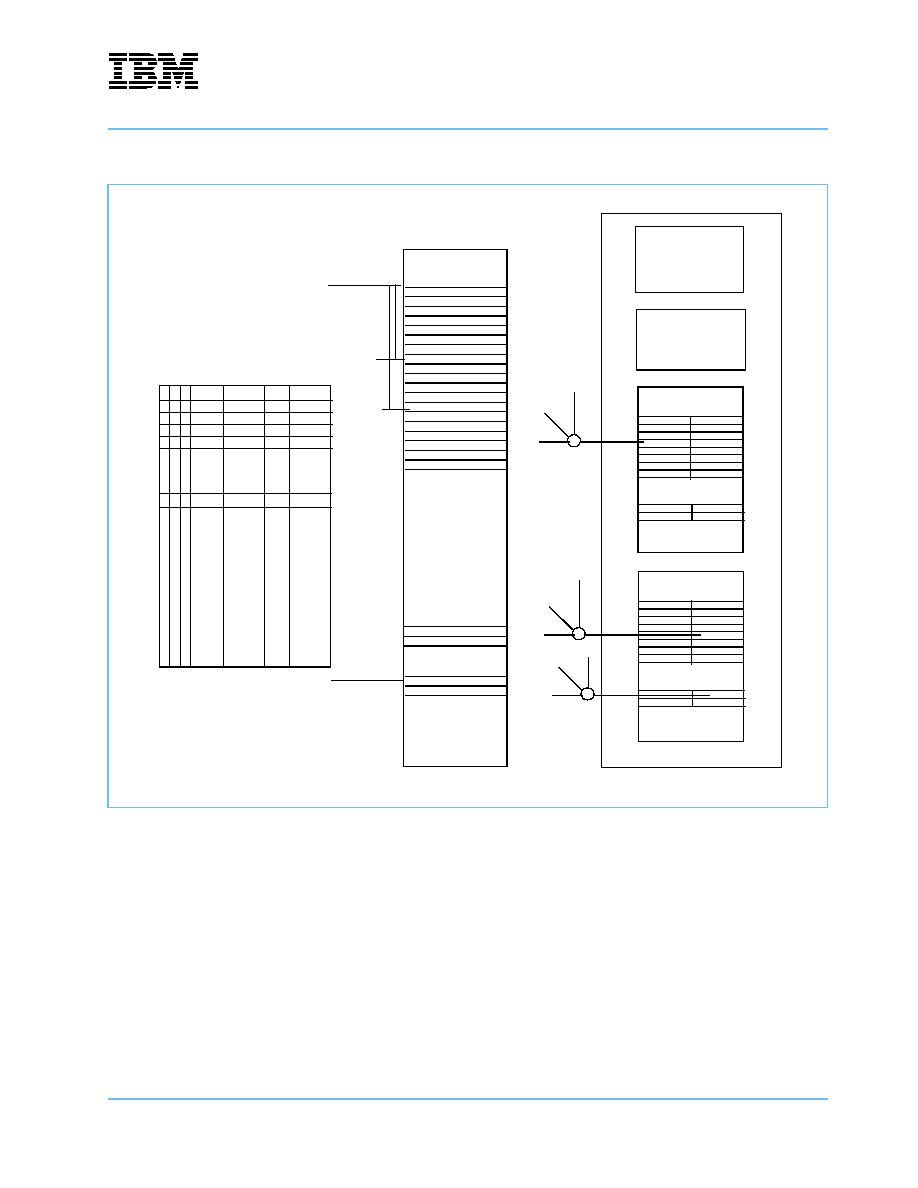
IBM PowerNP NP4GS3
Preliminary
Network Processor
np3_ds_sec08_tree.fm.11
January 29, 2003
Tree Search Engine
Page 329 of 605
8.2.4.6 SMT Trees
Software-managed (SMT) trees provide a mechanism to create trees that follow a Control Point Function
(CPF)-defined search algorithm such as an IP quintuple filtering table containing IPSA, IPDA, source port,
destination port, and protocol. SMT trees use the same PSCBs as FM trees, but only the first leaf following a
PSCB is shaped by the Table 8-17: LUDefTable Entry Definitions on page 333. The following leaves in a leaf
chain are shaped according to the five bits in the chaining pointer contained in the NLASMT leaf field (see
Table 8-13). Unlike FM and LPM, SMT trees allow leaves to specify ranges, for instance, that a source port
must be in the range of 100..110. SMT trees always contain two patterns of the same length in a leaf to define
a comparison range. When the first leaf is found after a PSCB, a compare-at-end operation is performed. If
OK, the search stops. If the comparison returns KO and the NLASMT field is non-zero, the next leaf is read
and another compare-at-end operation is performed. This process continues until an "OK" is returned or until
the NLASMT field is zero, which returns a KO.
Figure 8-6. Example Multibit LPM Tree Layout
Example (a) Multibit LPM tree
Assumptions:
DT: D3 (A & B) memory Only
1
L0
x
1
P0
N0
global_prefix_block_offset
P1
NBT01 (N1)
1
L1
x
0
P1
N1
(N1) NBT1
P1
P1
NBT1a (N1)
(N1) NBT1a
0
L3
x
0
P3
N3
P3
P3
NBT3a (N1)
D3A
D3B
D3C
D3D
Z0
D3A/B
Direct Table
PSCB
Prefix Block
global_prefix_block_offset
global_prefix_block_offset

IBM PowerNP NP4GS3
Network Processor
Preliminary
Tree Search Engine
Page 330 of 605
np3_ds_sec08_tree.fm.11
January 29, 2003
8.2.4.7 Compare-at-End Operation
The input key and the two reference patterns stored in each leaf can be logically divided into multiple fields
(see Figure 8-7 on page 330). One of two comparisons can be performed on each field:
1. Compare under mask. The input key bits are compared to Pattern0 bits under a mask specified in
Pattern1. A `1' in the mask means the corresponding bit in the input key must equal the corresponding bit
in Pattern0. A `0' means the corresponding bit in the input key has no influence on the comparison. The
entire field matches only when all bits match, in which case the TSE returns OK.
2. Compare under range. The input key bits are treated as an integer and checked to determine whether the
integer is within the range specified by Min and Max, inclusive. If so, the TSE returns OK, otherwise the
TSE returns KO.
When all fields return OK, the entire compare-at-end returns OK. Otherwise, KO returns. This operation uses
CompTableDef for definition and type of compare indication.
Logical field definitions are specified in the compare definition table CompDefTable. Table 8-14 shows the
entry format for the CompDefTable. Fields are compare-under-mask unless specified by the CompDefTable.
Each entry specifies one or two range comparisons, although multiple entries can specify more than two
range comparisons. Each range comparison is defined by offset and length parameters. The offset, which is
the position of the first bit in the field, must be at a 16-bit boundary and have a value of 0, 16, 32, 48, 64, 80,
96, 112, 128, 144, 160, 174, or 192. The length of the field must be 8, 16, 24, or 32 bits.
Table 8-13. NLASMT Field Format
1 bit
2 bits
3 bits
26 bits
Reserved
Width of next leaf
Height of next leaf
NLA (Next Leaf Address)
Figure 8-7. Example Input Key and Leaf Pattern Fields
IPSA
(32 bits)
IPDA
(32 bits)
SrcPort
(16 bits)
DstPort
(16 bits)
Prot
(8 bits)
Input
Key
Value
Value
Min
Min
Value
Leaf
Pattern0
Mask
Mask
Max
Max
Mask
Leaf
Pattern1
MinMax
Field1
Offset Field1
Offset Field0
Length
MinMax
Field0
Length

IBM PowerNP NP4GS3
Preliminary
Network Processor
np3_ds_sec08_tree.fm.11
January 29, 2003
Tree Search Engine
Page 331 of 605
In the input key shown in Figure 8-7: Example Input Key and Leaf Pattern Fields on page 330, the compare-
under-range for the Source Port (SrcPort) field would have Offset0 set to 64 and MinMaxLength0 set to 16.
The compare-under-range for the Destination (DstPort) field would have Offset1 set to 80 and
MinMaxLength1 set to 16. If more than two range comparisons are required, the Continue bit would be set to
1 so the next CompDefTable entry could be used for additional compare-under-range definitions.
The CompDefTable index used for tree comparisons is specified in the leaf Comp_Table_Index field (see
Table 8-7: SMT Tree Fixed Leaf Formats on page 318). Each compare-under-range operation takes one
clock cycle, so use as few compare-under-range operations as possible. If a range is a power of two, or
128-255, no compare-under-range is required since this range can be compared using compare-under-mask.
When a compare-at-end fails and the SMTNLA leaf field is not 0, the TSE reads the next leaf and performs
additional compare-at-end operations until the compare returns OK or until the SMTNLA is 0.
8.2.4.8 Ropes
As shown in the following figure, leaves in a tree can be linked together in a circular list called a rope. The first
field in a leaf is the chaining pointer, or the NLARope. Picocode can "walk the rope," or sequentially inspect all
leaves in a rope. Ropes can be created by setting the NLARope_En bit to `1' in the LUDefTable. See Table 8-
15: LUDefTable Rope Parameters on page 332.
Table 8-14. CompDefTable Entry Format
Field
Range
Bit Length
Value
Range 1 Offset (R1_Offset)
1
8
Starting bit position for first range compare.
It is defined by compare_table(35 to 28) bits but only 4 upper bits are used
to define the offset i.e (bits 35 to 32) and bits (31 to 28) are ignored.
Therefore, this field must be in 16 bit boundary
Range 1 Length (R1_Len)
1
8
Length and number of bits to be used as a part of range compare starting/
beginning from R1_Offset.This field is specified as the number of bits multi-
plied by 4. It is defined by compare_table(27 to 20) bits, but only 3 MSBs
are used to define the length (i.e. bits 27,26 & 25) and bits 24 to 20 are
ignored.
Range 2 Offset (R2_Offset)
2
8
Starting bit position for second range compare. It is defined by
compare_table(19 to 12) bits but only 4 upper bits are used to define the off-
set; i.e bits 19 to 16 and bits 15 to 12 are ignored. Therefore, this field must
be in 16-bit bound.
Range 2 Length (R2_Len)
2
8
Length and number of bits to be used as a part of range compare starting/
beginning from R2_Offset. This field is specified as the number of bits multi-
plied by 4.
It is defined by compare_table(11 to 4) bits but only 3 MSBs are used to
define the length (i.e. bits 11 to 9) and bits (8 to 4) are ignored.
Range 2 Valid (R2_Valid)
--
1
Range 2 Valid value. This field indicates whether or not the Range 2 Offset
and Length fields are valid.
0
Range 1 Offset and Length valid, but Range 2 Offset and Length not
valid.
1
Range 1 and Range 2 Offset and Length all valid.
It is defined by compare_table(3) bit.
Continue (Cont)
--
1
Continue indicator value. This field indicates whether the compare opera-
tion is continued in the next sequential entry of the table.
0
Comparison not continued
1 Comparison
continued
It is defined by compare_table(2) bit.

IBM PowerNP NP4GS3
Network Processor
Preliminary
Tree Search Engine
Page 332 of 605
np3_ds_sec08_tree.fm.11
January 29, 2003
Leaf insertion is always done between a RopeCLA and RopePLA. After insertion, the RopePLA is unchanged
and the RopeCLA points to the newly inserted leaf.
Leaf deletion is done two ways:
1. When the rope is not being walked, the rope is a single-chained linked list without a previous pointer.
Leaves cannot be deleted without breaking the linked list. Setting the DeletePending bit postpones the
deletion until the rope is walked again. A leaf is deleted by setting the DeletePending bit of the NLARope
field. In this case, leaves are completely deleted and leaf pattern searches will return a KO.
2. When the rope is being walked and the DeletePending bit is set, the TSE deletes the leaf automatically.
8.2.4.9 Aging
Aging is enabled whenever a rope is created. The NLARope field contains one aging bit that is set to `1' when
a leaf is created. When a leaf that matches the leaf pattern is found during a tree search, the TSE sets the
aging bit to `1' if it has not previously done so, and then writes this information to the control store. An aging
function controlled by a timer or other device can walk the rope to delete leaves with aging bits set to `0' and
then write the leaves to the control store with aging bits set to `0'. When no aging is desired, picocode should
not alter the aging bit, since bits set to `1' cannot be changed.
Figure 8-8. Rope Structure
Table 8-15. LUDefTable Rope Parameters
Parameter
Description
RopeCLA
Current leaf address in the rope. All TSE instructions related to the rope such as RCLR, ARDL and TLIR
(see Section 8.2.8 GTH Hardware Assist Instructions on page 359) relate to the leaf addressed by
RopeCLA.
RopePLA
Previous leaf address in the rope. Always the previous leaf if the rope is related to RopeCLA unless the
rope contains no leaf or one leaf. The following condition is always true for trees with two or more leaves:
RopePLA -> NLARope == RopeCLA.
LeafCnt
Leaf count - number of leaves in the tree
LeafTh
Leaf threshold causes an exception to be generated when the LeafCnt exceeds the threshold.
Leaf1
RopeCLA
TH
Leaf2
Leaf3
Leaf4
Leaf0
RopePLA
LeafCnt
Part of LUDefTable

IBM PowerNP NP4GS3
Preliminary
Network Processor
np3_ds_sec08_tree.fm.11
January 29, 2003
Tree Search Engine
Page 333 of 605
8.2.5 Tree Configuration and Initialization
8.2.5.1 The LUDefTable
The lookup definition table (LUDefTable), an internal memory structure that contains 128 entries to define
128 trees, is the main structure that manages the control store. The table indicates in which memory (DDR-
SDRAM, SRAM, or internal RAM) trees exist, whether caching is enabled, key and leaf sizes, and the search
type to be performed. Each DTEntry contains two indexes to the Pattern Search and Leaf Free Queue
(PSCB_Leaf_FQ). The first index defines which memory to use to create tree nodes, that is, where PSCBs
are located. The second defines which memory to use to create leaves within a tree. When an entry is added
to a tree, the memory required for the insert comes from the PSCB_Leaf_FQ and is returned when the entry
is deleted. For SMT trees, an LU_Def_Tbl can be defined to match a value into a given range, but an index to
an internal Compare Type Index must be given for the Compare Table (Cmp_Tbl).
Table 8-16. NLARope Field Format
2 bits
1 bit
2 bits
1 bit
26 bits
Reserved
Aging Counter
Reserved
Delete Pending
NLA (Next Leaf Address)
Table 8-17. LUDefTable Entry Definitions
(Page 1 of 4)
Field
Bit Length
Description
Cascade_entry/
Cache_entry
1
0
Normal tree entry (not a cache entry)
1
A Cascade/cache entry. When a search returns with KO, and Cache_entry = 1, TS
instructions will restart using the next entry in the LUDefTable (that is, LUDefIndex + 1).
Note: The LUDefIndex +1 entry must have this bit set to `0' (disabled) for NP4GS3B (R2.0).
The last LUDefIndex in the search chain entry must have this bit set to `0' (disabled) when
more than 1 table is cascaded. Cascading of more than 1 table is allowed in NP4GS3C
(R3.x).
Search_Type
2
Search Type value. This field indicates the type of search to be performed.
00 Full
Match
(FM).
01 Longest Prefix Match (LPM).
10 Software Managed Tree (SMT).
11 Reserved.
Hash_Type
4
Hash type
0000
No Hash
0001
192-bit IP Hash
0010
192-bit MAC Hash
0011
192-bit Network Dispatch Hash
0100
No Hash
0101
48-bit MAC Swap
0110
60-bit MAC Swap
0111
Reserved
1000
8-bit Hash
1001
12-bit Hash
1010
16-bit Hash
Note: When using Hash_Type 1000, 1001, and 1010, Hashedkey and HashedKey_length
will be extended by 8, 12, or 16 bits, respectively.
Color_En
1
Color Enable control value. This field controls whether the Color value is used to form the
hashed key value.
0
Color register not used.
1
Color register is used

IBM PowerNP NP4GS3
Network Processor
Preliminary
Tree Search Engine
Page 334 of 605
np3_ds_sec08_tree.fm.11
January 29, 2003
P1P2_Max_Size
5
Maximum size of Pattern1 and Pattern2 in leaf - Indicates size in half words (that is, 16 bits)
reserved for the "pattern" as a part of leaf in bytes. The maximum pattern size is 12, which
represents 192 bits.
P1P2_Max_size mapping:
00000
0 byte (no pattern)
00001
2 byte
00010
4 bytes
00011
6 bytes
00100
8 bytes
00101
10 bytes
00110
12 bytes
00111
14 bytes
01000
16 bytes
01001
18 bytes
01010
20 bytes
01011
22 bytes
01100
24 bytes
Others
0 byte (Reserved)
Notes:
For FM: Unused bits between p1p2_max_size - hkey_length must be initialized to zero.
For LPM: Unused bits between (p1p2_max_size - prefix_length) do not have to be initial-
ized and can be used by user data since these bits do not take part in the comparison.
For SMT: Unused bit between (2 * p1p2_max_size - 2 * Hashedkey_length) must be initial-
ized to zero.
NLARope_En
1
NLA Rope Enable control value. This field indicates whether or not the
leaf contains a Next Leaf Address Rope (NLA Rope) field.
0
Leaf does not contain NLARope field
1
Leaf contains NLARope field (enables aging)
PSCB_FQ_Index
6
Pattern Search Control Block Free Queue Index value. This is the index of the PSCB free
list.
Reserved
1
Reserved.
Dynamic_multibit_NBT_en
1
When set to `1', multibit NBT PSCB format is used during the search, enabling 1- or 4-bit
comparison at each PSCB node.
When set to `0', single-bit PSCB format (legacy) is used and only one bit will be tested at
each PSCB node.
This mode bit is available in NP4GS3C (R3.x)
DT_Base_Addr
26
Direct Table Base Address value.
Note: For NP4GS3C (R3.x), this field stores flat memory base_address for the MRD and
MWR commands with Shape_cntl = 01 (flat memory read/write). This base address and
Leaf_Height are used to compute the final address.
Table 8-17. LUDefTable Entry Definitions
(Page 2 of 4)
Field
Bit Length
Description

IBM PowerNP NP4GS3
Preliminary
Network Processor
np3_ds_sec08_tree.fm.11
January 29, 2003
Tree Search Engine
Page 335 of 605
DT_Size
4
Direct Table Size value - defines the number of DT entries within a memory bank.
0001
4 entries (2 bits)
0010
16 entries (4 bits)
0011
64 entries (6 bits)
0100
256 entries (8 bits)
0101
1 K entries (10 bits)
0110
4 K entries (12 bits)
0111
16 K entries (14 bits)
1000
32 K entries (15 bits)
1001
64 K entries (16 bits)
1010
128 K entries (17 bits)
1011
256 K entries (18 bits)
1100
512 K entries (19 bits)
1101
1 M (20 bits)
Others Reserved
Leaf_FQ_Index
6
Defines index of leaf free list
Leaf_Width
2 Leaf
width
Leaf_Height
3
Leaf height
Dynamic_leaf_shape_en
1
This option is valid for the TS_SMT and TS_FM commands.
When this mode is enabled, each primary leaf can have independent shape (size).
When this option is set to `0', for the FM and SMT search commands, the leaf shape is
defined as per the LUDef leaf_width and leaf_height parameters. Therefore, each primary
leaf has the same shape.
When this option is set to `1', the five least significant bits of the NBT field are used to
define the shape for that leaf. NBT bits 2:0 define the leaf_height parameter and bits 4:3
define the leaf_width. Also, the leaf_height and leaf_width parameters of the LUDef table
are ignored.
This mode bit is available in NP4GS3C (R3.x).
Leaf_read_Disable
1
This option is valid for the TS_LPM command.
When this option is set to `1', the LPM search algorithm (at the end of a successful search)
will not write the leaf contents to the Shared Memory Pool, and only the leaf address is
returned. A separate picocode memory read instruction is required to read the leaf content.
When this option is set to `0', the LPM search algorithm (at the end of the search) writes the
leaf contents back to the Shared Memory Pool and returns the leaf address.
This mode bit is available in NP4GS3C (R3.x).
LUDef_State
2
LUDef state - used by Product Software/User Code to indicate current status of the entry.
These bits do not affect Tree Search operation.
LUDef_Invalid
1
Indicates whether or not this entry is valid for normal Tree Search command or not. This bit
blocks any tree search while the tree is being built or swapped.
0 Valid
1
Invalid
When the LUDef Read request initiated by the Tree Search command finds this bit set to
`1', it will re-read this LUDefEntry every 16 cycles until it is set to Valid. This halts the tree
search for this particular thread.
Following fields are valid for GTH Only
RopeCLA
26
Current leaf address for rope.
Table 8-17. LUDefTable Entry Definitions
(Page 3 of 4)
Field
Bit Length
Description

IBM PowerNP NP4GS3
Network Processor
Preliminary
Tree Search Engine
Page 336 of 605
np3_ds_sec08_tree.fm.11
January 29, 2003
8.2.5.2 TSE Free Lists (TSE_FL)
The GTH has access to a set of 64 TSE free list control blocks, each defining a free list using the format
shown in Table 8-18. Free lists typically chain unused PSCBs and leaves into a linked list, but can also be
used by picocode to manage memory. The link pointer is stored in the control store at the address of the
previous list object. Objects stored in different memories and with different shapes should be placed in
different free lists. For example, a list of 64-bit PSCBs stored in both ZBT SRAM and internal RAM should
have different entries. The GTH thread executes the TSENQFL and TSDQFL commands to enqueue and
dequeue addresses on a free list. See Section 8.2.8.3 Tree Search Enqueue Free List (TSENQFL) on page
361 and Section 8.2.8.4 Tree Search Dequeue Free List (TSDQFL) on page 362.
A free list of N objects, each with shape of width = W, height = H and a start address of "A", is created by
enqueueing address A, A+H, A+2H, A+3H, ... A+(N-1)H in the free list. To prevent memory bottlenecks, free
lists can also be created in a "sprayed" manner for objects contained in SDRAM. For example, when
searching a large LPM tree with five PSCBs in a single bank, the bank must be accessed five times before
reaching a leaf. When the PSCBs are sprayed among multiple banks, the number of accesses remains iden-
tical but accesses are to multiple banks, thus eliminating bottlenecks.
RopePLA
26
Previous leaf address for rope
LeafCnt
26
Number of leaves in tree
LeafTh
10
Threshold for the number of leaves in a tree. If the LeafCnt is greater than or equal to this
assigned threshold, then a class 0 interrupt is generated (bit 9 of the class 0 interrupt vec-
tor). Checking of the threshold is performed only for the TLIR rope command.
The threshold is formed by the generation of two 26-bit numbers that are bit-wise ORed
resulting in a threshold value that is compared to the LeafCnt:
threshold(25:0) = 2**(LeafTh(9:5))or 2**(LeafTh(4:0))
Table 8-18. Free List Entry Definition
Field
Bit Length
Description
Head
26
Free list head address in the control store.
Tail
26
Free list tail address in the control store.
QCnt
26
Number of entries in the free list.
Threshold
5
Threshold value for the free list control block entry. This field is initialized to 0. The
threshold is determined as 2**Threshold. When the QCnt is less than or equal to
the threshold, a Class 0 interrupt (bit 8) is generated.
Table 8-17. LUDefTable Entry Definitions
(Page 4 of 4)
Field
Bit Length
Description

IBM PowerNP NP4GS3
Preliminary
Network Processor
np3_ds_sec08_tree.fm.11
January 29, 2003
Tree Search Engine
Page 337 of 605
8.2.6 TSE Registers and Register Map
Table 8-19. TSE Scalar Registers for GTH Only
(Page 1 of 3)
Name
Read/
Write
Hex
Address
Bit
Length
Description
Color
R/W
00
16
Color - see Section 8.2.1 Input Key and Color Register for FM and LPM Trees
on page 319 and Section 8.2.2 Input Key and Color Register for SMT Trees on
page 319.
LCBA0
R/W
02
26
Leaf Control Block Address 0 - typically contains the control store address of the
leaf in TSR0, but is also used as an address register for various TSE com-
mands.
LCBA1
R/W
03
26
Leaf Control Block Address 1 - typically contains the control store address of the
leaf in TSR1, but is also used as an address register for various TSE com-
mands.
DTA_Addr
R/W
04
26
DTEntry Address - valid after a hash has been performed.
DTA_Shape
R/W
05
5
Shape of a DTEntry - always (1,1) when direct leaves are disabled. Equals the
leaf shape as defined in LUDefTable when direct leaves are enabled.
Always set to `00000'.
HashedKeyLen
R/W
06
8
Pattern length minus 1 in HashedKey.
CacheFlags
R
07
3
See Section 8.2.3.3 Cascade/Cache on page 321.
NrPSCBs
R
08
8
See Section 8.2.3.3 Cascade/Cache on page 321.
Global_prefix_block_
offset
R/W
09
26
See Section 8.2.4.5 LPM Trees with Multibit Compare on page 326.
Available in NP4GS3C (R3.x).
HashedKey
R/W
0A-0F
192
Contains HashedKey
HashedKey 191_160
R/W
0A
32
Bits 191..160 of HashedKey
HashedKey 159_128
R/W
0B
32
Bits 159..128 of HashedKey
HashedKey 127_96
R/W
0C
32
Bits 127..96 of HashedKey
HashedKey 95_64
R/W
0D
32
Bits 95..64 of HashedKey
HashedKey 63_32
R/W
0E
32
Bits 63..32 of HashedKey
HashedKey 31_0
R/W
0F
32
Bits 31..0 of HashedKey

IBM PowerNP NP4GS3
Network Processor
Preliminary
Tree Search Engine
Page 338 of 605
np3_ds_sec08_tree.fm.11
January 29, 2003
LUDefCopy
R
10-12
96
Contains LU_Def_Table index in use and a copy of the following LU_Def_Table
fields:
Field
Bits
Definition
reserved
95:88
x`00' reserved
LU_Def_Index
87:80
Index of the location from where the
content was read.
For remaining field definitions, see Table 8-17: LUDefTable Entry Definitions on
page 333, with exceptions noted.
LU_Def_Invalid
79
LU_Def_State
78:77
Reserved
76:75
NP4GS3B (R2.0)
LPM_leaf_read_disable
76
available in NP4GS3C (R3.x)
Dynamic_leaf_shape_en
75
available in NP4GS3C (R3.x)
Leaf_Height
74:72
Leaf_Width
71:70
Leaf_FQ_Index
69:64
Reserved
63:62
DT_Size
61:58
DT_Base_Addr
57:32
Reserved
31:24
Dynamic_multibit_NBT_en 23
available
in
NP4GS3C (R3.x)
Reserved
22
PSCB_FQ_Index
21:16
Reserved
15:14
reserved
NLA_Rope_Ena
13
P1P2_Max_Size
12:8
Color_Ena
7
Hash_Type
6:3
Search_Type
2:1
Cascade/Cache Entry
0
LUDefCopy 95_64
R
10
32
Bits 95:64 of the LUDefCopy register
LUDefCopy 63_32
R
11
32
Bits 63..32 of LUDefCopy
LUDefCopy 31_0
R
12
32
Bits 31..0 of LUDefCopy
SetPatbit_GDH_4bit
R/W
1C
4
Contains 4 bits from the pattern stored in TSRx. Set by the SetPatBit_GDH com-
mand.
Valid for NP4GS3C (R3.x).
SetPatbit_GDH
R/W
1B
1
Contains one bit from the pattern stored in TSRx. Set by SetPatBit_GDH com-
mand.
Table 8-19. TSE Scalar Registers for GTH Only
(Page 2 of 3)
Name
Read/
Write
Hex
Address
Bit
Length
Description

IBM PowerNP NP4GS3
Preliminary
Network Processor
np3_ds_sec08_tree.fm.11
January 29, 2003
Tree Search Engine
Page 339 of 605
DistPosReg_GDH
R
1A
8
Contains result of DISTPOS command from DistPos_GDH
LUDefCopy_GDH
R
19
26
Contains LUDefTable index in use and a copy of the following LUDefTable
fields:
Dynamic_leaf_shape_en LUDefCopy_GDH(25) (valid for NP4GS3C (R3.x))
Reserved LUDefCopy_GDH(24,
23)
Reserved
LUDefCopy_GDH(22, 21)
P1P2_max_size
LUDefCopy_GDH(20 to 16)
DT_size
LUDefCopy_GDH(15 to 12)
NLARope_en
LUDefCopy_GDH(11)
color_en
LUDefCopy_GDH(10)
Tree_Type
LUDefCopy_GDH(9,8)
LuDefTable_index
LUDefCopy_GDH(7 to 0)
LUDefCopy_GDH 31_0
R
19
26
Bit 31..0 of LUDefCopy_GDH
Table 8-20. TSE Array Registers for All GxH
Name
Read/
Write
Starting Hex
Address
Ending Hex
Address
Bit
Length
Description
TSR0
R/W
32
47
2048
Tree Search Result Area 0
Note: Portion of the data overlaps with TSR1
TSR1
R/W
40
47
1024
Tree Search Result Area 1
Note: Portion of the data overlaps with TSR0
TSR2
R/W
48
63
2048
Tree Search Result Area 2
Note: Portion of the data overlaps with TSR3
TSR3
R/W
56
63
1024
Tree Search Result Area 3
Note: Portion of the data overlaps with TSR2
Note: In this table, starting and ending Address represents the offset for a given thread's starting address in the Shared Memory Pool.
Table 8-21. TSE Registers for GTH (Tree Management)
Name
Read/
Write
Hex
Address
Bit
Length
Description
PatBit_TSR0
R/W
1E
1
Contains one bit from the pattern stored in TSR0. Set by TRS0PAT command.
DistPosReg
R
1F
8
Contains result of DISTPOS command
LURopeCopyTH
R
13
10
Contains copy of LeafTH field of LUDefTable
LURopeCopyQCnt
R
14
26
Contains copy of LeafCnt field of LUDefTable
LURopeCopyPrev
R
15
26
Contains copy of RopePLA field of LUDefTable
LURopeCopyCurr
R
16
26
Contains copy of RopeCLA field of LUDefTable
Table 8-19. TSE Scalar Registers for GTH Only
(Page 3 of 3)
Name
Read/
Write
Hex
Address
Bit
Length
Description

IBM PowerNP NP4GS3
Network Processor
Preliminary
Tree Search Engine
Page 340 of 605
np3_ds_sec08_tree.fm.11
January 29, 2003
Table 8-22. TSE Scalar Registers for GDH and GTH
Name
Read/
Write
Hex
Address
Bit
Length
Description
LCBA0
R/W
02
31
Leaf Control Block Address 0 - typically contains the control store address of the
leaf in TSRx, but is also used as an address register for various TSE commands.
Bits 30:26
The Leaf Control Block Address Shape which is used by CMPEND
instruction only
Bits 25:0
Leaf Control Block Address
LCBA1
R/W
03
31
Leaf Control Block Address 1 - typically contains the control store address of the
leaf in TSRx, but is also used as an address register for various TSE commands.
Bits 30:26
The Leaf Control Block Address Shape which is used by CMPEND
instruction only
Bits 25:0
Leaf Control Block Address
CacheFlags
R
07
3
See Section 8.2.3.3 Cascade/Cache on page 321
NrPSCBs
R
08
8
See Section 8.2.3.3 Cascade/Cache on page 321.
SetPatbit_GDH
R
1B
1
Contains one bit from the pattern stored in TSRx. Set by SetPatBit_GDH command.
Global_prefix_block_
offset
R/W
09
26
See Section 8.2.4.5 LPM Trees with Multibit Compare on page 326.
Available in NP4GS3C (R3.x).
SetPatbit_GDH_4bit
R
1C
4
Contains four bits from the pattern stored in TSRx. Set by the SetPatBit_GDH com-
mand.
Available in NP4GS3C (R3.x).
DistPosReg_GDH
R
1A
8
Contains result of DISTPOS command from DistPos_GDH
LUDefCopy_GDH
R
19
26
Contains LUDefTable index in use and a copy of the following LUDefTable fields:
Dynamic_leaf_shape_en LUDefCopy_GDH(25) (valid for NP4GS3C (R3.x))
Reserved LUDefCopy_GDH(24,23)
Reserved
LUDefCopy_GDH(22,21)
P1P2_max_size
LUDefCopy_GDH(20 to 16)
DT_size
LUDefCopy_GDH(15 to 12)
NLARope_en
LUDefCopy_GDH(11)
color_en
LUDefCopy_GDH(10)
Tree_Type
LUDefCopy_GDH(9,8)
LuDefTable_index
LUDefCopy_GDH(7 to 0)
Table 8-23. PSCB Register Format
Field
Bit Length
Control Store Address for PSCB
NPA0
26
Next PSCB address - pointer to next PSCB in tree for PSCB part 0
NBT0
8
Next bit to test for PSCB part 0
LCBA0
26
Leaf control block address: Pointer to leaf for PSCB part 0
NPA1
26
Next PSCB address - Pointer to next PSCB in tree for PSCB part 1
NBT1
8
Next bit to test for PSCB part 1
LCBA1
26
Leaf control block address - Pointer to leaf for PSCB part 1
Index
8
Index of current PSCB physically stored in previous PSCB
PatBit
1
Value of HashedKey[Index] based on value of index field in PSCB register

IBM PowerNP NP4GS3
Preliminary
Network Processor
np3_ds_sec08_tree.fm.11
January 29, 2003
Tree Search Engine
Page 341 of 605
Table 8-24. TSE GTH Indirect Registers
Indirect Register
Bit Length
Description
Notes
PSCBx.NPA_HK
26
Selects either the NPA0 field from PSCBx or the NPA1 field depending on value of
register PSCBx.Index
1, 2, 3
PSCBx.NPA_TSR0
26
Selects either the NPA0 field from PSCBx or the NPA1 field depending on value of
register PatBit_TSR0. (Register PatBit_TSR0 must have been initialized previously
using TSR0PAT command)
1, 2, 4
PSCBx.NBT_HK
8
Selects either the NBT0 field from PSCBx or the NBT1 field depending on value of
register PSCBx.Index
1, 2, 3
PSCBx.NBT_TSR0
8
Selects either the NBT0 field from PSCBx or the NBT1 field depending on value of
register PatBit_TSR0
1, 2, 4
PSCBx.LCBA_HK
26
Selects either the LCBA0 field from PSCBx or the LCBA1 field depending on value
of register PSCBx.Index
1, 2, 3
PSCBx.LCBA_TSR0
26
Selects either the LCBA0 field from PSCBx or the LCBA1 field, depending on value
of register PatBit_TSR0
1, 2, 4
PSCBx.NotNPA_HK
26
Selects either the NPA0 field from PSCBx or the NPA1 field depending on inverse
value of register PSCBx.Index
1, 2, 3
PSCBx.NotNPA_TSR0
26
Selects either the NPA0 field from PSCBx or the NPA1 field depending on inverse
value of register PatBit_TSR0
1, 2, 4
PSCBx.NotNBT_HK
8
Selects either the NBT0 field from PSCBx or the NBT1 field depending on inverse
value of register PSCBx.Index
1, 2, 3
PSCBx.NotNBT_TSR0
8
Selects either the NBT0 field from PSCBx or the NBT1 field depending on inverse
value of register PatBit_TSR0
1, 2, 4
PSCBx.NotLCBA_HK
26
Selects either the LCBA0 field from PSCBx or the LCBA1 field depending on
inverse value of register PSCBx.Index
1, 2, 3
PSCBx.NotLCBA_TSR0
26
Selects either the LCBA0 field from PSCBx or the LCBA1 field depending on
inverse value of register PatBit_TSR0
1, 2, 4
1. x must equal 0, 1, or 2.
2. The Indirect registers of the TSE select, via dedicated hardware assist, one of the TSE registers listed in Section 8.2.6 TSE Regis-
ters and Register Map on page 337. The Indirect registers appear in the TSE Register Map with a unique register number.
3. PSCBx.Index points to a specific bit in the HashedKey. The bit's value determines whether the 0 or 1 part of PSCBx will be read or
written.
4. Value of PatBit_TSR0 determines whether the 0 or 1 part of PSCBx will be read or written.
Table 8-25. Address Map for PSCB0-2 Registers in GTH
(Page 1 of 2)
PSCBx
Read/Write
PSCB0
PSCB1
PSCB2
Size
NPA0
R/W
80
A0
C0
26
NBT0
R/W
81
A1
C1
8
LCBA0
R/W
82
A2
C2
26
NPA1
R/W
84
A4
C4
26
NBT1
R/W
85
A5
C5
8
LCBA1
R/W
86
A6
C6
26
Addr
R/W
88
A8
C8
26
Index
R/W
89
A9
C9
8
PatBit
R
8B
AB
CB
1

IBM PowerNP NP4GS3
Network Processor
Preliminary
Tree Search Engine
Page 342 of 605
np3_ds_sec08_tree.fm.11
January 29, 2003
8.2.7 TSE Instructions
The Tree Search Engine (TSE) provides facilities for conducting and managing tree searches. Two TSE
coprocessor interfaces are provided for each thread: TSE0 and TSE1. Therefore, each thread can issue
instructions to each of these TSE0 and TSE1 resources.
General TSE instructions can be executed by both TSE0 and TS1 in any thread.
NPA_HK
R/W
90
B0
D0
26
NBT_HK
R/W
91
B1
D1
8
LCBA_HK
R/W
92
B2
D2
26
NotNPA_HK
R/W
94
B4
D4
26
NotNBT_HK
R/W
95
B5
D5
8
NotLCBA_HK
R/W
96
B6
D6
26
NPA_TSR0
R/W
98
B8
D8
26
NBT_TSR0
R/W
99
B9
D9
8
LCBA_TSR0
R/W
9A
BA
DA
26
NotNPA_TSR0
R/W
9C
BC
DC
26
NotNBT_TSR0
R/W
9D
BD
DD
8
NotLCBA_TSR0
R/W
9E
BE
DE
26
Table 8-26. General TSE Instructions
Opcode
Command
Detail Section
0
Null
1
TS_FM
8.2.7.1 FM Tree Search (TS_FM) on page 343
2
TS_LPM
8.2.7.2 LPM Tree Search (TS_LPM) on page 344
3
TS_SMT
8.2.7.3 SMT Tree Search (TS_SMT) on page 346
4
MRD
8.2.7.4 Memory Read (MRD) on page 347
5
MWR
8.2.7.5 Memory Write (MWR) on page 348
6
HK
8.2.7.6 Hash Key (HK) on page 349
7
RDLUDEF
8.2.7.7 Read LUDefTable (RDLUDEF) on page 350
8
COMPEND
8.2.7.8 Compare-at-End (COMPEND) on page 352
9
DistPos_GDH
8.2.7.9 DistinguishPosition for Fast Table Update (DISTPOS_GDH) on page 353
10
RDPSCB_GDH
8.2.7.10 Read PSCB for Fast Table Update (RDPSCB_GDH) on page 354
11
WRPSCB_GDH
8.2.7.11 Write PSCB for Fast Table Update (WRPSCB_GDH) on page 356
12
SetPatBit_GDH
8.2.7.12 SetPatBit_GDH on page 357
13 to 15
Reserved
Note: Commands can be executed by all GxHs with threads.
Table 8-25. Address Map for PSCB0-2 Registers in GTH
(Page 2 of 2)
PSCBx
Read/Write
PSCB0
PSCB1
PSCB2
Size

IBM PowerNP NP4GS3
Preliminary
Network Processor
np3_ds_sec08_tree.fm.11
January 29, 2003
Tree Search Engine
Page 343 of 605
8.2.7.1 FM Tree Search (TS_FM)
Figure 8-9. General Layout of TSE Fields in Shared Memory Pool
Table 8-27. FM Tree Search Input Operands
Operand
Bit Length
Operand Source
Description
Direct
Indirect
LUDefIndex
8
Imm16(12..5)
GPR(7..0)
Defines entry in LUDefTable that controls the search.
LCBANr
1
Imm16(0)
Imm12(0)
0
search results are stored in TSRx/LCBA0.
1
search results are stored in TSRx/LCBA1.
TSEDPA
4
Imm16(4..1)
Imm12(4..1)
TSE Thread Shared Memory Pool Address. Stores location of Key, Key-
Length, and Color and determines Leaf destination. The TSEDPA is the
high order 4 bits of the thread's shared memory pool address (see
7.2.4 Shared Memory Pool on page 196) and is constrained to be on a
four-QW boundary. Use only values of x`8', x`A', x`C', and x`E'.
Key
192
Shared Memory Pool
Pattern to be searched, located in Shared Memory Pool.
The key must be initialized only in the byte boundary of the key length.
KeyLength
8
Shared Memory Pool
Length of pattern minus 1 in key. Must be initialized before search.
Located in shared memory pool.
Color
16
Shared Memory Pool
Used only when enabled in LUDefTable. Must be initialized before
search. Located in Shared Memory Pool.
Following is available for GTH only.
UseLUDefCopyReg
1
Imm16(13)
Imm12(5)
Enables TSE read of LUDefCopy register. Can save clock cycles, espe-
cially when RDLUDEF is executed asynchronously with the picocode
that sets the key.
0
TSE reads LUDefTable.
1
TSE does not read the LUDefTable and uses information con-
tained in LUDefCopy register. Assumes LUDefTable was read pre-
viously using RDLUDEF.
LUDefCopy
96
Register
Input only when UseLUDefCopyReg is `1'.
leaf userdata
Pattern (103..0) from Leaf
leaf userdata
Pattern (191..104) from Leaf
prefix
NLA Rope
Reserved
DTA
shape
DTA (26 bits)
HashedKey(191..104)
Reserved
HashedKey(103..0)
HkeyLen
Reserved
Reserved
KeyLen
color
Key(191 ..96)
Key (95 ..0)
127
119
111
95
31
0
31
87
23
7
0
TSEDPA
TSEDPA+1
TSEDPA+2
TSEDPA+3
TSEDPA+4
TSEDPA+5
63
127
96
121
(5 bits)
TSEDPA+6
TSEDPA+7

IBM PowerNP NP4GS3
Network Processor
Preliminary
Tree Search Engine
Page 344 of 605
np3_ds_sec08_tree.fm.11
January 29, 2003
8.2.7.2 LPM Tree Search (TS_LPM)
Table 8-28. FM Tree Search Results (TSR) Output
Result
Bit Length
Source
Description
OK/KO
1
Flag
0
KO: Unsuccessful Operation.
1
OK: Successful Operation.
TSRx
512
Shared Memory Pool
When OK/KO is `1', leaf is read and stored in TSRx.
TSRx is mapped into the Shared Memory pool, at an offset of 4 QW
past the starting QW indicated by the input TSEDPA parameter. That is,
the Shared Memory Pool QW location = TSEDPA*4 + 4
LCBA0 / 1
26
Register
When OK/KO is `1', leaf address is stored in LCBA0 / 1.
CacheFlags
3
Register
See Section 8.2.3.3 Cascade/Cache on page 321.
NrPSCBs
8
Register
See Section 8.2.3.3 Cascade/Cache on page 321.
LUDefCopy_GDH
26
Register
Contains LUDefTable index in use and a copy of the following
LUDefTablefields:
Dynamic_leaf_shape_en LUDefCopy_GDH(25) (NP4GS3C (R3.x))
Reserved LUDefCopy_GDH(24,23)
Reserved LUDefCopy_GDH(22,21)
P1P2_max_size
LUDefCopy_GDH(20 to 16)
DT_size
LUDefCopy_GDH(15 to 12)
NLARope_en LUDefCopy_GDH(11)
color_en LUDefCopy_GDH(10)
Tree_Type LUDefCopy_GDH(9,8)
LuDefTable_index
LUDefCopy_GDH(7 to 0)
Will be stored in scalar register and its address in Register Address Map
is `019'.
Following is available for GTH only.
LUDefCopy
96
Register
Output only when UseLUDefCopyReg is `0'. Set to contents of
LUDefTable at entry pointed to by LUDefIndex.
Table 8-29. LPM Tree Search Input Operands
(Page 1 of 2)
Operand
Bit Length
Operand Source
Description
Direct
Indirect
LUDefIndex
8
Imm16(12..5)
GPR(7..0)
Defines entry in LUDefTable used to control the search
LCBANr
1
Imm16(0)
Imm12(0)
0
search results are stored in TSRx/LCBA0
1
search results are stored in TSRx/LCBA1
TSEDPA
4
Imm16(4..1)
Imm12(4..1)
TSE Thread Shared Memory Pool Address. Stores location of Key, Key-
Length, and Color and determines Leaf destination. The TSEDPA is the
high order 4 bits of the thread's shared memory pool address (see
7.2.4 Shared Memory Pool on page 196) and is constrained to be on a
four-QW boundary. Use only values of x`8', x`A', x`C', and x`E'.
Key
192
Shared Memory Pool
Pattern to be searched, located in Shared Memory Pool.
The key must be initialized only in the byte boundary of the key length.
KeyLength
8
Shared Memory Pool
Length of pattern minus 1 in key. Must be initialized before search.
Located in shared memory pool.
Color
16
Shared Memory Pool
Used only when enabled in LUDefTable. Must be initialized before
search. Located in Shared Memory Pool.

IBM PowerNP NP4GS3
Preliminary
Network Processor
np3_ds_sec08_tree.fm.11
January 29, 2003
Tree Search Engine
Page 345 of 605
global_prefix_block_
offset
20
Register
Contains global prefix offset used by Multibit LPM trees.
Required when Dynamic_multibit_NBT_en is enabled.
Will be stored in scalar register, and its address in the Register Address
Map is X`009'.
(valid for NP4GS3C (R3.x)).
Following is available for GTH only.
UseLUDefCopyReg
1
Imm16(13)
Imm12(5)
Enables TSE read of LUDefCopy register
Can save clock cycles, especially when RDLUDEF is executed asyn-
chronously with the picocode that sets the key.
0
TSE reads LUDefTable
1
TSE does not read the LUDefTable and uses information con-
tained in LUDefCopy register. Assumes LUDefTable was read pre-
viously using RDLUDEF.
Note: UseLUDefCopyReg = `1' is not supported for LUDefEntry with
Cache_enable.
LUDefCopy
96
Register
Input only when UseLUDefCopyReg is `1'. Set to contents of
LUDefTable at entry given by LUDefIndex.
Table 8-30. LPM Tree Search Results Output
Result
Bits
Source
Description
OK/KO
1
Flag
0
KO: Unsuccessful Operation
1
OK: Successful Operation
TSRx
512
Shared Memory Pool
When OK/KO is `1', leaf is read and stored in TSRx
TSRx is mapped into the Shared Memory pool, at an offset of 4 QW
past the starting QW indicated by the input TSEDPA parameter.
That is, Shared Memory Pool QW location = TSEDPA*4 + 4
LCBA0 / 1
26
Register
When OK/KO is `1', leaf address is stored in LCBA0 / 1
CacheFlags
3
Register
See Section 8.2.3.3 Cascade/Cache on page 321
NrPSCBs
8
Register
See Section 8.2.3.3 Cascade/Cache on page 321
LUDefCopy_GDH
26
Register
Contains LUDefTable index in use and a copy of the following
LUDefTablefields:
Dynamic_leaf_shape_en LUDefCopy_GDH(25) (valid for NP4GS3C
(R3.x))
Reserved LUDefCopy_GDH(24,23)
Reserved
LUDefCopy_GDH(22,21)
LP1P2_max_size
LUDefCopy_GDH(20 to 16)
DT_size
LUDefCopy_GDH(15 to 12)
NLARope_en
LUDefCopy_GDH(11)
color_en
LUDefCopy_GDH(10)
Tree_Type
LUDefCopy_GDH(9,8)
LuDefTable_index
LUDefCopy_GDH(7 to 0)
Will be stored in scalar register, and its address in the Register Address
Map is `019'.
The following is available for GTH only.
LUDefCopy
96
Register
Output only when UseLUDefCopyReg is `0'. Set to contents of
LUDefTable at entry given by LUDefIndex.
Table 8-29. LPM Tree Search Input Operands
(Page 2 of 2)
Operand
Bit Length
Operand Source
Description
Direct
Indirect

IBM PowerNP NP4GS3
Network Processor
Preliminary
Tree Search Engine
Page 346 of 605
np3_ds_sec08_tree.fm.11
January 29, 2003
8.2.7.3 SMT Tree Search (TS_SMT)
Table 8-31. SMT Tree Search Input Operands
Operand
Bit Length
Operand Source
Description
Direct
Indirect
LUDefIndex
8
Imm16(12..5)
GPR(7..0)
Defines entry in LUDefTable used to control the search
LCBANr
1
Imm16(0)
Imm12(0)
0
search results are stored in TSRx/LCBA0
1
search results are stored in TSRx/LCBA1
TSEDPA
4
Imm16(4..1)
Imm12(4..1)
TSE Thread Shared Memory Pool Address - stores location of Key,
KeyLength, and Color and determines Leaf destination. The TSEDPA is
the high order 4 bits of the thread's shared memory pool address (see
7.2.4 Shared Memory Pool on page 196) and is constrained to be on a
four-QW boundary. Use only values of x`8', x`A', x`C', and x`E'.
Key
192
Shared Memory Pool
Pattern to be searched, located in shared memory pool.
The key must be initialized only in the byte boundary of the key length.
KeyLength
8
Shared Memory Pool
Length of pattern minus 1 in key. Must be initialized before search.
Located in shared memory pool.
Color
16
Shared Memory Pool
Used only when enabled in LUDefTable. Must be initialized before
search. Located in shared memory pool.
Following is available for GTH only.
UseLUDefCopyReg
1
Imm16(13)
Imm12(5)
Enables TSE read of LUDefCopy register
Can save clock cycles, especially when RDLUDEF is executed asyn-
chronously with the picocode that sets the key.
0
TSE reads LUDefTable
1
TSE does not read the LUDefTable and uses information con-
tained in LUDefCopy register. Assumes LUDefTable was read previ-
ously using RDLUDEF.
Note: UseLUDefCopyReg = `1' is not supported for LUDefEntry with
Cache Enable.
LUDefCopy
96
Register
Input only when UseLUDefCopyReg is `1'. Set to contents of
LUDefTable at entry given by LUDefIndex.
Table 8-32. SMT Tree Search Results Output
(Page 1 of 2)
Result
Bit Length
Source
Description
OK/KO
1
Flag
0
KO: Unsuccessful Operation
1
OK: Successful Operation
TSRx
512
Shared Memory Pool
When OK is `1', leaf is read and stored in TSRx.
TSRx is mapped into the Shared Memory pool, at an offset of 4 QW
past the starting QW indicated by the input TSEDPA parameter.
That is, Shared Memory Pool QW location = TSEDPA*4 + 4
LCBA0 / 1
26
Register
When OK is `1', leaf address is stored in LCBA0 / 1
CacheFlags
3
Register
See Section 8.2.3.3 Cascade/Cache on page 321
NrPSCBs
8
Register
See Section 8.2.3.3 Cascade/Cache on page 321

IBM PowerNP NP4GS3
Preliminary
Network Processor
np3_ds_sec08_tree.fm.11
January 29, 2003
Tree Search Engine
Page 347 of 605
8.2.7.4 Memory Read (MRD)
The memory read command provides direct read capability from any location in the control store. LCBA0 / 1
provide the full read address. Shape is provided by the LUDefTable (for Leaf or PSCB) or directly as part of
the command field for the object. The content to be read is stored in TSRx. When flat memory mode
(shape_cntl = 01) is selected, the 20 least significant bits in LCBA0/1 contain the offset that is used with leaf
shape and DT_Base_Addr from the LUDefTable to compute the final address to be read. In flat memory
mode, the following rules are applied:
� The 20 least significant bits in LCBA0/1 can be used as an offset; the remaining bits are ignored.
� Valid leaf shape heights are 1, 2, and 4; no other heights are supported.
� During final address computation, address spanning is not allowed.
Flat memory mode is valid for NP4GS3C (R3.x).
LUDefCopy_GDH
26
Register
Contains LUDefTable index in use and a copy of the following
LUDefTablefields:
Dynamic_leaf_shape_en LUDefCopy_GDH(25) (valid for NP4GS3C
(R3.x))
Reserved
LUDefCopy_GDH(24,23)
Reserved
LUDefCopy_GDH(22,21)
P1P2_max_size
LUDefCopy_GDH(20 to 16)
DT_size
LUDefCopy_GDH(15 to 12)
NLARope_en
LUDefCopy_GDH(11)
color_en
LUDefCopy_GDH(10)
Tree_Type
LUDefCopy_GDH(9,8)
LuDefTable_index
LUDefCopy_GDH(7 to 0)
Will be stored in scalar register, and its address in Register Address
Map is `019'.
Following are available for GTH only.
LUDefCopy
96
Register
An output only when UseLUDefCopyReg is `0'. Set to contents of
LUDefTable at entry given by LUDefIndex.
Table 8-32. SMT Tree Search Results Output
(Page 2 of 2)
Result
Bit Length
Source
Description

IBM PowerNP NP4GS3
Network Processor
Preliminary
Tree Search Engine
Page 348 of 605
np3_ds_sec08_tree.fm.11
January 29, 2003
8.2.7.5 Memory Write (MWR)
The memory write command provides direct write capability to any location in the control store. LCBA0 / 1
provide the full write address. Shape is provided by the LUDefTable (for Leaf or PSCB) or directly as part of
the command field for the object. The content to be written is stored in TSRx. When flat memory mode
(shape_cntl = 01) is selected, the 20 least significant bits in LCBA0/1 contain the offset that is used with leaf
shape and DT_Base_Addr from the LUDefTable to compute the final address to be read. In flat memory
mode, the following rules are applied:
� The 20 least significant bits in LCBA0/1 can be used as an offset; the remaining bits are ignored.
� Valid leaf shape heights are 1, 2, and 4; no other heights are supported.
� During final address computation, address spanning is not allowed.
Table 8-33. Memory Read Input Operands
Operand
Bit Length
Operand Source
Description
Direct
Indirect
ShapeCtrl
2
Imm16(14..13)
GPR(9..8)
00
Direct shape.
01
Flat mode. Leaf_shape_height and DT_base_addr from
LuDefTable are used with the LCBA0/1 field to compute the
address to be read. Leaf shape from LuDefTable is used as a
shape. When this mode is selected, the final address to be read
= DT_base_addr + (LCBA0/1 * Leaf_shape_height). (Valid for
NP4GS3C (R3.x))
10
PSCB shape is based on address and tree type from LudefT-
able. That is, LPM tree type and ZBT or H1 address shape will
be set to (1x2), and for any other case, shape will be set to
(1x1).
11
Leaf shape from LUDefTable
LUDefIndex
8
Imm16(12..5)
GPR(7..0)
LUDefTable entry used to read shape information. Valid only when
ShapeCtrl is `01', `10' or `11'.
Width
2
Imm16(9..8)
GPR(4..3)
Width of object to be read. Valid only when ShapeCtrl is `00'.
Height
3
Imm16(7..5)
GPR(2..0)
Height of object to be read. Valid only when ShapeCtrl is `00'.
TSEDPA
4
Imm16(4..1)
Imm12(4..1)
TSE Thread Shared Memory Pool Address determines the destina-
tion location for the data to be read. The TSEDPA is the high order 4
bits of the thread's shared memory pool address (see 7.2.4 Shared
Memory Pool on page 196) and is constrained to be on a four-QW
boundary.
LCBANr
1
Imm16(0)
Imm12(0)
0
Address to be read is LCBA0
1
Address to be read is LCBA1
LCBA0 / 1
26
Register
Address to be read when ShapeCtrl is set to `00', `10', or `11'.
For NP4GS3C (R3.x), this operand contains the offset used for
address computation when ShapeCtrl is set to `01'.
Table 8-34. Memory Read Output Results
Result
Bit Length
Source
Description
TSRx
512
Shared Mem-
ory Pool
TSRx is mapped into the Shared Memory pool, starting at the QW indicated by the
input TSEDPA parameter for a length of 4 QW.
OK/KO
1
Flag
0
KO: Unsuccessful Operation
1
OK: Successful Operation

IBM PowerNP NP4GS3
Preliminary
Network Processor
np3_ds_sec08_tree.fm.11
January 29, 2003
Tree Search Engine
Page 349 of 605
Flat memory mode is valid for NP4GS3C (R3.x).
8.2.7.6 Hash Key (HK)
Table 8-35. Memory Write Input Operands
Operand
Bit Length
Operand Source
Description
Direct
Indirect
ShapeCtrl
2
Imm16(14..13)
GPR(9..8)
00
Direct Shape
01
Flat mode. Leaf_shape_height and DT_base_addr from LuDefTable
are used with LCBA0/1 field to compute the address to be written.
Leaf shape from LuDefTable is used as a shape. When this mode is
selected, final address to be written = DT_base_addr + (LCBA0/1 *
Leaf_shape_height). (Valid for NP4GS3C (R3.x)).
10
PSCB shape is based on address and tree type from LudefTable.
That is, LPM tree type and ZBT or H1 address shape will be set to
(1x2), and for any other case, shape will be set to (1x1).
11
Leaf shape from LUDefTable
LUDefIndex
8
Imm16(12..5)
GPR(7..0)
LUDefTable entry used to read shape information. Valid only when
ShapeCtrl is `01', `10' or `11'.
Width
2
Imm16(9..8)
GPR(4..3)
Width of object to be written. Valid only when ShapeCtrl is `00'.
Height
3
Imm16(7..5)
GPR(2..0)
Height of object to be written. Valid only when ShapeCtrl is `00'.
TSEDPA
4
Imm16(4..1)
Imm12(4..1)
TSE Thread Shared Memory Pool Address determines the source location
for the data to be written. The TSEDPA is the high order 4 bits of the
thread's shared memory pool address (see 7.2.4 Shared Memory Pool on
page 196) and is constrained to be on a four-QW boundary.
LCBANr
1
Imm16(0)
Imm12(0)
0
Address to be written is LCBA0
1
Address to be written is LCBA1
LCBA0 / 1
26
Register
Address to be read when ShapeCtrl is set to `00', `10', or `11'.
For NP4GS3C (R3.x), this operand contains the offset used for address
computation when ShapeCtrl is set to `01'.
TSRx
512
Shared Memory Pool
Data to be written. TSRx is mapped into the Shared Memory pool, starting
at the QW indicated by the input TSEDPA parameter for a length of 4 QW.
Table 8-36. Hash Key Input Operands
Operand
Bit Length
Operand Source
Description
Direct
Indirect
LUDefIndex
8
Imm16(12..5)
GPR(7..0)
Defines entry in LUDefTable containing Hash Type
TSEDPA
4
Imm16(4..1)
Imm12(4..1)
TSE Thread Shared Memory Pool Address - stores location of Key, Key-
Length, and Color and determines Hash Key destination. The TSEDPA is the
high order 4 bits of the thread's shared memory pool address (see
7.2.4 Shared Memory Pool on page 196) and is constrained to be on a four-
QW boundary. Use only values of x`8', x`A', x`C', and x`E'.
Direct_
HashType_En
1
Imm16(0)
Imm12(0)
Enable Direct HashType definition
0
HashType defined by LUDefEntry
1
HashType defined via command
Direct_
HashType
4
Imm16(8..5)
GPR(3..0)
Use defined Hash Type for Hashing. Valid when Direct_HashType_En = 1

IBM PowerNP NP4GS3
Network Processor
Preliminary
Tree Search Engine
Page 350 of 605
np3_ds_sec08_tree.fm.11
January 29, 2003
8.2.7.7 Read LUDefTable (RDLUDEF)
RDLUDEF reads LUDefTable at a specified entry and stores the result in the LUDefCopy register field in the
shared memory pool.The TSE can read LUDefTable while picocode builds a key because RDLUDEF is
executed asynchronously.
Key
192
Shared Memory Pool
Pattern to be searched, located in Shared Memory Pool.
The key must be initialized only in the byte boundary of the key length.
KeyLen
8
Shared Memory Pool
Defines length of pattern minus 1 in key. Must be initialized before search.
Located in the Shared Memory Pool.
Color
16
Shared Memory Pool
Must be initialized before search - used only when enabled in LUDefTable.
Located in the shared memory pool.
Invalid when Direct_HashType_En is set to value `1'.
Table 8-37. Hash Key Output Results
Result
Bit Length
Source
Description
HashedKeyReg
192
Shared
Memory
Pool
Hashed key register - contains the HashedKey (including color when enabled in
LUDefTable) according to Section 8.2.1 Input Key and Color Register for FM and LPM
Trees on page 319 and Section 8.2.2 Input Key and Color Register for SMT Trees on
page 319. Hash function is defined in the LUDefTable.
Stored in the Shared Memory Pool QW location = TSEDPA*4 + 2 & 3.
HashedKeyLen
8
Shared
Memory
Pool
Hashed key length contains the length of pattern minus 1 in HashedKeyReg. Stored in
the shared memory pool QW location = TSEDPA*4 + 3 bit (7:0).
DTA
26
Shared
Memory
Pool
DTEntry Address. Stored in shared memory pool QW location = TSEDPA*4 + 2, bits
(121:96).
Note: Not valid when Direct_HashType_En is set to value `1'.
OK/KO
1
Flag
0
KO: Unsuccessful Operation
1
OK: Successful Operation
LUDefCopy_GDH
26
Register
Contains LUDefTable index in use and a copy of the following
LUDefTablefields:
Dynamic_leaf_shape_en LUDefCopy_GDH(25) (valid for NP4GS3C (R3.x))
Reserved LUDefCopy_GDH(24,23)
Reserved
LUDefCopy_GDH(22,21)
P1P2_max_size
LUDefCopy_GDH(20 to 16)
DT_size
LUDefCopy_GDH(15 to 12)
NLARope_en
LUDefCopy_GDH(11)
color_en
LUDefCopy_GDH(10)
Tree_Type
LUDefCopy_GDH(9,8)
LuDefTable_index
LUDefCopy_GDH(7 to 0)
Will be stored in scalar register, and its address in Register Address Map is `019'.
The following is available for GTH only.
LUDefCopy
96
Register
Set to contents of LUDefTable at entry given by LUDefIndex.
Table 8-36. Hash Key Input Operands
Operand
Bit Length
Operand Source
Description
Direct
Indirect

IBM PowerNP NP4GS3
Preliminary
Network Processor
np3_ds_sec08_tree.fm.11
January 29, 2003
Tree Search Engine
Page 351 of 605
Figure 8-10. General Layout of TSE RDLUDEF in Shared Memory Pool
Table 8-38. RDLUDEF Input Operands
Operand
Bit Length
Operand Source
Description
Direct
Indirect
LUDefIndex
8
Imm16(12..5)
GPR(7..0)
Defines entry in LUDefTable
TSEDPA
4
Imm16(4..1)
Imm12(4..1)
TSE Thread Shared Memory Pool Address determines the destination
location for the LUDefTable entry data to be read. The TSEDPA is the
high order 4 bits of the thread's shared memory pool address (see
7.2.4 Shared Memory Pool on page 196) and is constrained to be on a
four-QW boundary.
Table 8-39. RDLUDEF Output Results
Result
Bit Length
Source
Description
LUDefCopy
88
Shared
Memory Pool
Set to contents of LUDefTable at entry given by LUDefIndex and stored in shared
memory pool. The entry is placed into two QW starting at the QW indicated by the
TSEDPA. The entry is right-justified with the most significant bits padded with 0.
Various fields of LUDefEntry are at the same bit position as in the LUDefTable mem-
ory.
119:112 LUDefIndex that corresponds to the LUDefEntry.
111:32
LUDefEntry contents
They are left-justified.
Note: TSEDPA address and TSEDPA + 1 will be overwritten during this command.
Contents of LUDefCopy will be returned at TSEDPA and contents of LUDefCopy_Rope
will be returned in the next address. LUDefCopy_Rope content will be valid for the GTH
thread.
LUDefCopy_GDH
26
Register
Contains LUDefTable index in use and a copy of the following LUDefTablefields:
Dynamic_leaf_shape_en LUDefCopy_GDH(25) (valid for NP4GS3C (R3.x))
Reserved LUDefCopy_GDH(24,
23)
Reserved
LUDefCopy_GDH(22, 21)
P1P2_max_size
LUDefCopy_GDH(20 to 16)
DT_size
LUDefCopy_GDH(15 to 12)
NLARope_en
LUDefCopy_GDH(11)
color_en
LUDefCopy_GDH(10)
Tree_Type
LUDefCopy_GDH(9,8)
LuDefTable_index
LUDefCopy_GDH(7 to 0)
Will be stored in scalar register and its address in Register Address Map is `019'.
OK/KO
1
Flag
0
KO: Unsuccessful Operation
1
OK: Successful Operation
LuDefIndex
LUDefTable Entry (79..32)
LUDefTable_Rope Entry (95 ..0) (GTH only)
127
120 119
112
0
TSEDPA
TSEDPA+1
111
Reserved
95
Reserved
Reserved
32
31

IBM PowerNP NP4GS3
Network Processor
Preliminary
Tree Search Engine
Page 352 of 605
np3_ds_sec08_tree.fm.11
January 29, 2003
8.2.7.8 Compare-at-End (COMPEND)
COMPEND performs a compare-at-end operation for SMT trees. After a tree search command has
performed a full search including a COMPEND, picocode can obtain a pointer to another leaf chain from the
leaf and start another COMPEND on the leaf chain. The first leaf chain could contain leaves with filtering
information, and the second could contain leaves with quality of service information. COMPEND should be
used only after a tree search command. The COMPEND command uses Key instead of HashedKey during
operation, since it is assumed that hashing is not needed for SMT. Hence, the Key field is read by the
command, not the HashedKey field. For NP4GS3B (R2.0), it is necessary to initialize the unused key bits to
zero because hashing is not done on the Key and it is used "as is." For NP4GS3C (R3.x), it is not necessary
to initialize the unused key bits to zero.
Table 8-40. COMPEND Input Operands
Operand
Bit Length
Operand Source
Description
Direct
Indirect
LUDefIndex
8
Imm16(12:5)
GPR(7:0)
Defines the entry in the LuDefTable.
LCBNANr
1
Imm16(0)
Imm12(0)
0
Search results are stored in TSRx/LCBA0
1
Search results are stored in TSRx/LCBA1
TSEDPA
4
Imm16(4..1)
Imm12(4..1)
TSE Thread Shared Memory Pool Address - stores location of Key,
KeyLength, and Color and determines Leaf destination. The TSEDPA
is the high order 4 bits of the thread's shared memory pool address
(see 7.2.4 Shared Memory Pool on page 196) and is constrained to be
on a four-QW boundary. Use only values of x`8', x`A', x`C', and x`E'.
LCBA0 / 1
31
Register
Start address of leaf chain and its shape.
Bits:
30:29
Leaf Width
28:26
Leaf Height
25:0
Leaf Address
Note: A Valid Leaf Width and Leaf Height must be provided with the
Leaf Address.
Key
192
Shared Memory Pool
Input of previous tree search command located in the Shared Memory
Pool at an offset of 0 and 1QW from the QW indicated by the TSEDPA.
KeyLen
8
Shared Memory Pool
Input of previous tree search command located in the Shared Memory
Pool at the QW indicated by the TSEDPA
Table 8-41. COMPEND Output Results
Result
Bit Length
Source
Description
OK/KO
1
Flag
0
KO: Unsuccessful Operation
1
OK: Successful Operation
TSRx
512
Shared Mem-
ory Pool
When OK is `1', leaf is read and stored in TSRx
When OK is `0', last leaf of chain is stored in TSRx
TSRx is mapped into the Shared Memory pool, starting at an offset of 4 QW past the
QW indicated by the input TSEDPA parameter for a length of 4 QW.
LCBA0 / 1
26
Register
When OK is `1', leaf address is stored in LCBA0 / 1
When OK is `0', leaf address of last leaf in chain is stored in LCBA0 / 1
Note: Shape for the corresponding leaf will not be valid when LCABA0/1 is read.
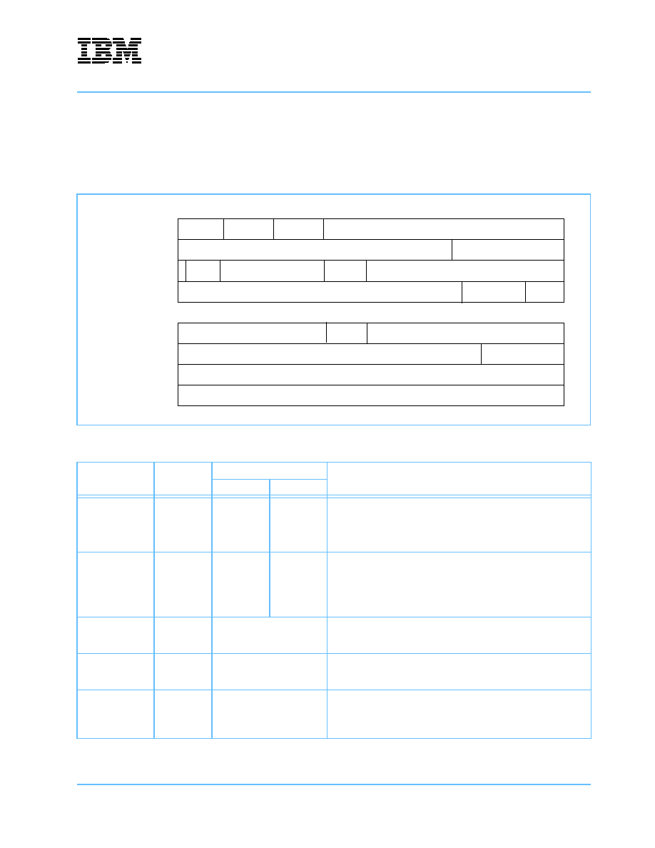
IBM PowerNP NP4GS3
Preliminary
Network Processor
np3_ds_sec08_tree.fm.11
January 29, 2003
Tree Search Engine
Page 353 of 605
8.2.7.9 DistinguishPosition for Fast Table Update (DISTPOS_GDH)
DISTPOS_GDH performs a pattern compare between the pattern stored in HashedKey of the shared
memory pool and a pattern from the leaf specified in TSRx. The result is stored in the DistPosReg_GDH
register. The OK flag is set when a full match has been detected.
Figure 8-11. Shared Memory Pool with DISTPOS_GDH Command Subfields
Table 8-42. DISTPOS_GDH Input Operands
Operand
Bit Length
Operand Source
Description
Direct Indirect
TSEDPA_leaf
4
Imm16(4..1)
Imm12(4..1)
Indicates the leaf storage location in the Thread Shared Memory
Pool. The TSEDPA_leaf is the high order 4 bits of the thread's
shared memory pool address (see 7.2.4 Shared Memory Pool on
page 196) and is constrained to be on a four-QW boundary. Use only
values of x `8', x `A', x `C', and x `E'.
TSEDPA_HK
4
Imm16(8..5)
Imm12(8..5)
Indicates the HashedKey storage location in the Thread Shared
Memory Pool. The TSEDPA is the high order 4 bits of the thread's
shared memory pool address (see 7.2.10 Shared Memory Pool) and
is constrained to be on a four-QW boundary. Use only values of x `8',
x `A', x `C', and x `E'. Hashedkey is assumed to be stored at TSEDPA
+2 location in shared memory pool.
HashedKey
192
Shared Memory Pool
Contains the hashed pattern and it will be stored at TSEDPA_HK +2
(7..0) quad word location. The structure of the Hashed Key in shared
memory pool is shown in Figure 8-11.
HashedKeyLen
8
Shared Memory Pool
Contains length of hashed pattern minus 1. Stored at TSEDPA_HK
+2 quad word location. Structure of Hashed Key in shared memory
pool is shown in Figure 8-11.
TSRx
512
Shared Memory Pool
Contains second pattern with pattern length (for LPM & FM only).
TSRx is mapped into the shared memory pool, starting at an offset of
4 QW past the QW indicated by the input TSEDPA_leaf parameter
for a length of 4 QW.
leaf userdata
Pattern (103..0) from Leaf
leaf userdata
Pattern (191..104) from Leaf
prefix
NLA Rope
Reserved
DTA
shape
DTA (26 bits)
HashedKey (191..104)
Reserved
HashedKey (103..0)
HkeyLen
Reserved
Reserved
KeyLen
color
Key (191 ..96)
Key (95 ..0)
127
119
111
95
31
0
31
87
23
7
0
TSEDPA_HK
TSEDPA_HK+1
TSEDPA_HK+2
TSEDPA_HK+3
TSEDPA_leaf
TSEDPA_leaf+1
63
12
7
96
121
(5 bits)
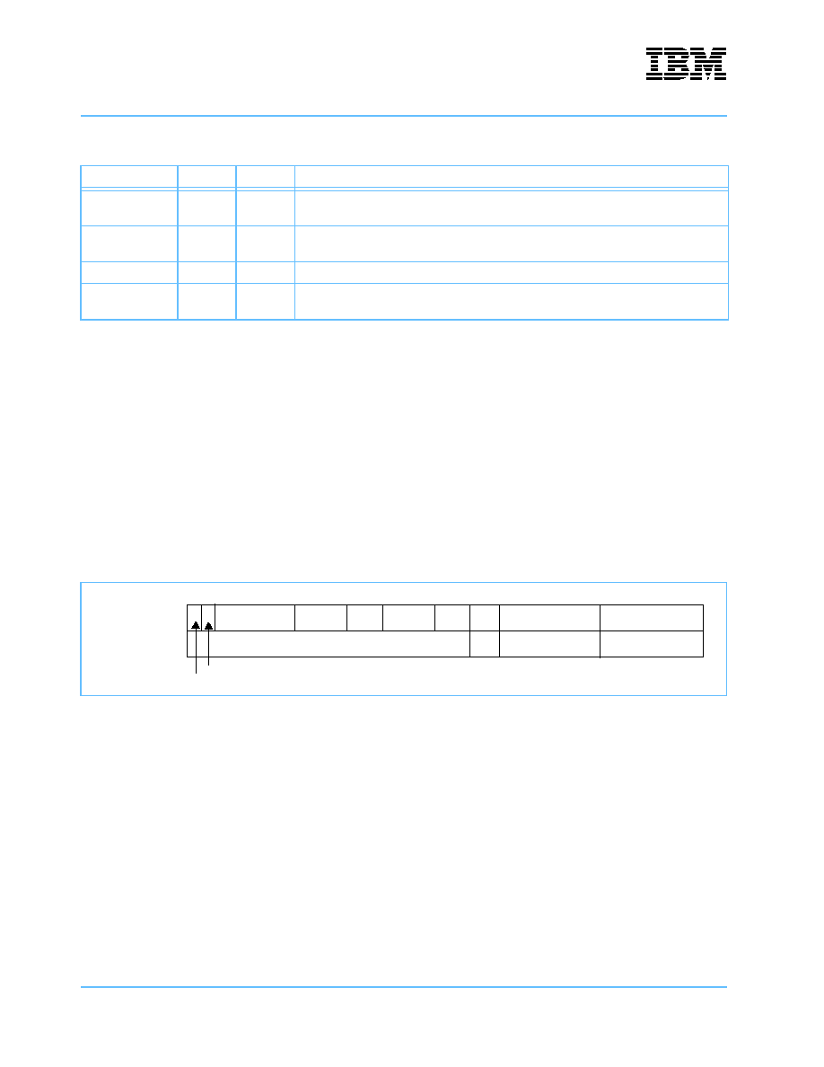
IBM PowerNP NP4GS3
Network Processor
Preliminary
Tree Search Engine
Page 354 of 605
np3_ds_sec08_tree.fm.11
January 29, 2003
DISTPOS_GDH applies to LPM and FM only. It needs P1P2_Max_Size value as a part of the computation.
The value is assumed to be valid prior to this command. This value is stored as a scalar register, and is inde-
pendent for each thread.
8.2.7.10 Read PSCB for Fast Table Update (RDPSCB_GDH)
RDPSCB_GDH reads a PSCB from the control store and stores it in one of the PSCBx locations in the
shared memory pool. For LPM, the entire PSCB is read from memory at the address given by PSCB.Addr
and stored in PSCB. For FM, the entire PSCB is read from memory and converted into a LPM PSCB format
and either NPA0/1 or LCBA0/1 will be set to all zero, since only one of the fields will be valid. This command
is not supported for SMT.
Structure for PSCB register shared memory pool is as follows:
Table 8-43. DISTPOS_GDH Output Results
Result
Bit Length
Source
Description
OK/KO
1
Flag
0
Pattern does not match
1
Pattern in HashedKey matches pattern in TSRx
DistPosReg_GDH
8
Scalar
register
Smallest bit position where pattern in HashedKey differs from pattern in TSRx.
Will be stored in scalar register and its address in the Register Address Map is `01A'.
OK/KO
1
Flag
0
KO: Unsuccessful Operation
1
OK: Successful Operation
Figure 8-12. Shared Memory Pool with PSCB Subfields
LCBA1
Address
Reserved Index
NPA0
Reserved
127
87
95
31
0
PSCBx
DPA
63
DPA+1
Reserved
79
Patbit
72
71
LCBA0
NPA1
NP1
NP0
rdwrpscb_LPM_compact_PSCB_en (valid for NP4GS3C (R3.x))
Reserved (5 bits)
(26 bits)

IBM PowerNP NP4GS3
Preliminary
Network Processor
np3_ds_sec08_tree.fm.11
January 29, 2003
Tree Search Engine
Page 355 of 605
Table 8-44. RDPSCB_GDH Input Operands
Operand
Bit Length
Operand Source
Description
Direct Indirect
DPA_PSCB
6
Imm16(5..0) Imm12(5..0)
The DPA_PSCB is a Full address of the7.2.4 Shared Memory Pool on
page 196. This indicates working address of the PSCB register.
Full PSCB will occupy 2 quadwords from shared memory pool. This
address must start at an even address.
RdWrPSCB_Cntl
2
Imm16(7..6) Imm12(7..6)
00 Result is based on PatBit value in the shared memory pool as
shown in above diagram.
PatBit = 0 Branch 0 entry of the PSCB is read
PatBit = 1 Branch 1 entry of the PSCB is read
01 Branch 0 entry of the PSCB is read
10 Branch 1 entry of the PSCB is read
11 Branch 0 and branch 1 entry of the PSCB is read
Reserved
1
Imm16(8)
Imm12(8)
Reserved.
PSCB.Addr
26
Shared Memory Pool
(121..96)
Address to be read in control store of the PSCB. This is stored in
shared memory pool.
PSCB.rdwrps_LPM_
compact_PSCB_en
1
Shared Memory Pool (127)
This optional argument for LPM reduces memory read bandwidth.
When not used, it must be set to `0'.
This option enables use of the LPM compact PSCB.
It indicates the LPM DT/PSCB entry has no valid leaf address and is
stored in memory that is 36 bits wide or less than 64 bits wide (that is,
Z0 and H1 SRAM memories). It is not used by FM or SMT.
0
For FM PSCB/DT and when LPM DT/PSCB is stored in 64-bit or
wider memory for width = 1 and height = 1 (DDR DRAM mem-
ory).
1
When LPM DT/PSCB is stored in memory that is narrower than
64 bits for width = 1 and height = 1 (36-bit Z0 and H1 SRAM
memories).
When this argument is set to `1', PSCB.Addr+0 and PSCB.Addr+2 are
treated as one PSCB pair. PSCB.Addr+1 and PSCB.Addr+3 are
treated as separate PSCB pair. Addresses are interleaved for a given
pair.
When this argument is set to `1', the TSE reads only the PSCB.Addr
location for 0 branch and the PSCB.addr+2 location for 1 branch.
It is assumed that PSCB.Addr+1 and PSCB.Addr+3 are used as a
PSCB pair by some other PSCB node.
PSCB.Addr.LCBA is ignored and Address will is read in the Control
Store using a 1x1 shape. The contents of the PSCB.LCBA in the
Shared Memory Pool are set to zero. This argument is stored in the
Shared Memory Pool.
This argument is valid for NP4GS3C (R3.x).
Note: This command needs the value of the Search_type field for PSCB shape computation. Since the LUDefTable entry is not read
during this command, it uses the content from the local copy of the LUDefCopy_GDH register. The values in the LuDefCopy_GDH
register are assumed to be valid prior to this command. This value is stored as a scalar register and is independent for each thread
coprocessor.

IBM PowerNP NP4GS3
Network Processor
Preliminary
Tree Search Engine
Page 356 of 605
np3_ds_sec08_tree.fm.11
January 29, 2003
8.2.7.11 Write PSCB for Fast Table Update (WRPSCB_GDH)
WRPSCB_GDH writes a PSCB stored in PSCBx (in shared memory pool) to the control store. For LPM, the
entire PSCB is written to memory to the address given by PSCB.Addr. For FM, the PSCB is written to
memory in FMPSCB format. In both cases, WRPSCB_GDH generates the PSCB's two format bits. When the
PSCB represents a DTEntry, only half of PSCB is written to memory. That is, the entire DTEntry is written by
picocode. This command is not supported for SMT. pscb_cntl/format bits (which defines end node or valid
presence of leaf) for the DT/PSCB entry will be computed based on the content of PSCB.LCBA0/1 and no
checking/validation is performed, based on the PSCB.NPA0/1 or PSCB.NBT0/1, therefore PSCB.NBT0/1 will
be written to memory as is and for LPM PSCB.NPA0/1 is written as is.
Table 8-45. RDPSCB_GDH Output Results
Result
Bit Length
Source
Description
PSCB
--
Register
PSCB is read from control store and stored in register PSCB<pn>. NPA0, NBT0, LCBA0 and
NPA1, NBT1, LCBA1 fields are changed. Remainders are not changed.
For FM: Content of either NPA0 or LCBA0 and NPA1 or LCBA1 will be set to zero (that is,
either NPA and LCBA will be valid). Also content of NBT0 will be set to zero when NPA0 is
zero and NBT1 will be set to zero when NPA1 is zero (that is, for end node NBT and NPA is
not valid).
For LPM: No validation is performed based on the actual content of LCBA, NBT, NPA or for-
mat fields.
OK/KO
1
Flag
0
KO: Unsuccessful Operation
1
OK: Successful Operation
Table 8-46. WRPSCB_GDH Input Operands
(Page 1 of 2)
Operand
Bit Length
Operand Source
Description
Direct Indirect
DPA_PSCB
6
Imm16(5..0)
Imm12(5..0)
The DPA_PSCB is a Full address of the 7.2.4 Shared Memory Pool
on page 196. This indicates that the working address of the PSCB
register Full PSCB will occupy 2 quadwords from the shared mem-
ory pool.
This address must start at an even address.
RdWrPSCB_Cntl
2
Imm16(7..6)
Imm12(7..6)
00 Action is based on PatBit value.
PatBit = 0 Branch 0 entry of the PSCB is written
PatBit = 1 Branch 1 entry of the PSCB is written
01 Branch 0 entry of the PSCB is written
10 Branch 1 entry of the PSCB is written
11 Branch 0 and branch 1 entry of the PSCB is written
Reserved
1
Imm16(8)
Imm12(8)
Reserved.
PSCB.Addr
26
Shared Memory Pool
(121..96)
Address to be written in control store of the PSCB. This is stored in
shared memory pool.

IBM PowerNP NP4GS3
Preliminary
Network Processor
np3_ds_sec08_tree.fm.11
January 29, 2003
Tree Search Engine
Page 357 of 605
8.2.7.12 SetPatBit_GDH
SetPatBit_GDH instruction reads a bit from the HashedKey pattern or Leaf Reference pattern stored in TSRx
of the shared memory pool and stores this bit in the SetPatBit_GDH register. Picocode must copy it to the
appropriate patbit field of TSEDPA_PSCBx of the shared memory pool.
PSCB.rdwrpscb_LPM
_compact_PSCB_en
1
Shared Memory Pool (127)
This optional argument for LPM reduces memory read bandwidth.
When not used, it must be set to `0'.
This option enables use of the LPM compact PSCB.
It indicates the LPM DT/PSCB entry has no valid leaf address and
is stored in memory that is 36 bits wide or less than 64 bits wide
(that is, Z0 and H1 SRAM memories). It is not used by FM.
0
For FM PSCB/DT and when LPM DT/PSCB is stored in 64-bit
or wider memory for width = 1 and height = 1 (DDR DRAM
memory).
1
When LPM DT/PSCB is stored in memory that is narrower
than 64 bits for width = 1 and height = 1 (36-bit Z0 and H1
SRAM memories) and No Prefix/LCBA is present.
When this argument is set to `1', PSCB.Addr+0 and PSCB.Addr+2
are treated as one PSCB pair. PSCB.Addr+1 and PSCB.Addr+3
are treated as separate PSCB pair. Addresses are interleaved for a
given pair.
When this argument is set to `1', the TSE reads only the
PSCB.Addr location for 0 branch and the PSCB.addr+2 location for
1 branch.
It is assumed that PSCB.Addr+1 and PSCB.Addr+3 are used as a
PSCB pair by some other PSCB node.
PSCB.Addr.LCBA is ignored and Address will is read in the Control
Store using a 1x1 shape. The contents of the PSCB.LCBA in the
Shared Memory Pool are set to zero. This argument is stored in the
Shared Memory Pool.
This argument is valid for NP4GS3C (R3.x).
PSCB
--
Shared Memory Pool
The PSCB is read from the Shared Memory Pool PSCB<pn> and
written to the Control Store. Some or all of the NPA0, NBT0,
LCBA0, NPA1, NBT1, and LCBA1 fields are used.
For FM: The contents of NPA0, LCBA0 and NPA1, or LCBA1 are
used (that is, either NPA and LCBA is valid). The contents of NBT0
are set to zero when NPA0 is 0, and NBT1 is set to zero when
NPA1 is 0 (that is, end-node NBT and NPA are not valid).
For LPM: When LCBA contents are zero (that is, no valid leaf/prefix
is present), format bits will be set to `00'. No validation is performed
based on the content of NBT or NPA fields and written to the Con-
trol Store.
Note: This command needs the value of the Search_type field for PSCB shape computation. Since the LuDefTable entry is not read
during this command, it uses the content from the local copy of the LUDefCopy_GDH register. The values in the LuDefCopy_GDH
register are assumed to be valid prior to this command. This value is stored as a scalar register and is independent for each thread
coprocessor.
Table 8-47. WRPSCB_GDH Output Results
Result
Bit Length
Source
Description
OK/KO
1
Flag
0
KO: Unsuccessful Operation
1
OK: Successful Operation
Table 8-46. WRPSCB_GDH Input Operands
(Page 2 of 2)
Operand
Bit Length
Operand Source
Description
Direct Indirect

IBM PowerNP NP4GS3
Network Processor
Preliminary
Tree Search Engine
Page 358 of 605
np3_ds_sec08_tree.fm.11
January 29, 2003
SetPatBitGDH_4Bit is used by tree management code for multibit NBT LPM search trees and is valid for
NP4GS3C (R3.x).
Table 8-48. SetPatBit_GDH Input Operands
Operand
Bit Length
Operand Source
Description
Direct Indirect
DPA_PSCB
6
Imm16(5..0)
Imm12(5..0)
The DPA_PSCB is a Full address of the thread's shared address
(see 7.2.4 Shared Memory Pool on page 196). This indicates the
working address of the PSCB register. The DPA_PSCBx.index field
will be used.
TSEDPA_HK_leaf
4
Imm16(9..6)
Imm12(9..6)
Indicates the leaf or HashedKey storage location in the Thread
Shared Memory pool. The TSEDPA is the high order 4 bits of the
thread's shared memory pool address (see 7.2.4 Shared Memory
Pool on page 196) and is constrained to be on a four-QW boundary.
Use only values of x `8', x `A', x `C', and x `E'.
When HK_Leaf_flag = 0, HashedKey will be used for this operation.
When HK_Leaf_flag = 1, Leaf content will be used for operation.
When Leaf is to be used, Location for leaf will be TSEDPA_HK_leaf;
and when HashedKey is used, Location for HashedKey will be
TSEDPA_HK_leaf +2.
HK_leaf_flag
1
Imm16(10)
Imm12(10)
When HK_Leaf_flag = 0, HashedKey will be used for this operation
and TSEDPA_HK_leaf +2 will be used as a HashedKey Location in
shared memory pool.
When HK_Leaf_flag = 1, Leaf content will be used for operation and
TSEDPA_HK_leaf will be used as a Leaf location in shared memory
pool.
HashedKey
192
Shared Memory Pool
Contains the hashed pattern, and it will be stored at
TSEDPA_HK_leaf +2 & +3 QW location. Structure of Hashed Key in
shared memory pool is shown in the above figure.
HashedKeyLen
8
Shared Memory Pool
Contains length of hashed pattern minus 1, and it will be stored at
TSEDPA_HK_leaf +3 (7..0) QW location. Structure of Hashed Key in
shared memory pool is shown in the above figure.
TSRx
512
Shared Memory Pool
Contains second pattern with pattern length (for LPM only). TSRx is
mapped into the Shared Memory pool, starting at an offset of 4 QW
past the QW indicated by the input TSEDPA_HK_leaf parameter, for
a length of 4 QW.
Table 8-49. SetPatBit_GDH Output Results
Result
Bit Length
Source
Description
SetPatBit_GDH
1
Register
Smallest bit position in which the pattern in HashedKey differs from the pattern in the
leaf at TSEDPA_HK_leaf location. Its address in register address map is x'01B'.
SetPatBit_GDH_4bit
4
Register
Smallest four bit positions where the pattern in HashedKey differs from the pattern in
leaf at TSEDPA_HK_leaf location. Its address in register address map is x'01C'. This
register is valid for NP4GS3C (R3.x).
Note: This command needs the value of the p1p2_max_size value as a part of its computation. Since the LUDefTable entry is not read
during this command, it uses the contents from the local copy of the LUDefCopy_GDH register. The values in the LuDefCopy_GDH reg-
ister are assumed to be valid prior to this command. This value is stored as a scalar register and is independent for each thread copro-
cessor. SetPatBit_GDH applies to LPM only.

IBM PowerNP NP4GS3
Preliminary
Network Processor
np3_ds_sec08_tree.fm.11
January 29, 2003
Tree Search Engine
Page 359 of 605
8.2.8 GTH Hardware Assist Instructions
GTH Hardware Assist instructions can be executed only by the GTH thread (1) on TSE0. General TSE
instructions (see Table 8-26 on page 342) cannot execute concurrently with GTH Hardware Assist instruc-
tions.
GTH Hardware Assist instructions are used to perform tree management functions such as insert and delete
operations. The general TSE instruction set is also able to perform these functions, but they require additional
code steps. For applications requiring a high rate of tree insert and delete operations, the use of the general
TSE instruction set is recommended because multiple threads can be employed. Other tree management
functions (such as aging, which employs ARDL and TLIR) or memory management functions (which employs
TSENQFL and TSDQFL) can be performed using software-created and managed structures.
Table 8-50. General GTH Instructions
Opcode
Command
Detail Section
16
HK_GTH
8.2.8.1 Hash Key GTH (HK_GTH) on page 360
17
RDLUDEF_GTH
8.2.8.2 Read LUDefTable GTH (RDLUDEF GTH) on page 360
18
TSENQFL
8.2.8.3 Tree Search Enqueue Free List (TSENQFL) on page 361
19
TSDQFL
8.2.8.4 Tree Search Dequeue Free List (TSDQFL) on page 362
20
RCLR
8.2.8.5 Read Current Leaf from Rope (RCLR) on page 362
21
ARDL
8.2.8.6 Advance Rope with Optional Delete Leaf (ARDL) on page 363
22
TLIR
8.2.8.7 Tree Leaf Insert Rope (TLIR) on page 364
23
Reserved
24
CLRPSCB
8.2.8.8 Clear PSCB (CLRPSCB) on page 364
25
RDPSCB
8.2.8.9 Read PSCB (RDPSCB) on page 365
26
WRPSCB
8.2.8.10 Write PSCB (WRPSCB) on page 365
27
PUSHPSCB
8.2.8.11 Push PSCB (PUSHPSCB) on page 367
28
DISTPOS
8.2.8.12 Distinguish (DISTPOS) on page 367
29
TSR0PAT
8.2.8.13 TSR0 Pattern (TSR0PAT) on page 368
30
PAT2DTA
8.2.8.14 Pattern 2DTA (PAT2DTA) on page 368
31
Reserved
Note: The instructions listed in this table can only be executed by the GTH.

IBM PowerNP NP4GS3
Network Processor
Preliminary
Tree Search Engine
Page 360 of 605
np3_ds_sec08_tree.fm.11
January 29, 2003
8.2.8.1 Hash Key GTH (HK_GTH)
8.2.8.2 Read LUDefTable GTH (RDLUDEF GTH)
RDLUDEF reads the LUDefTable at a specified entry and stores the result in the LUDefCopy register. The
TSE can read LUDefTable while picocode builds a key because RDLUDEF is executed asynchronously.
Once the key is ready, the tree search execution can be executed with the UseLUDefCopyReg flag set to `1'.
Table 8-51. Hash Key GTH Input Operands
Operand
Bit Length
Operand Source
Description
Direct
Indirect
LUDefIndex
8
Imm16(12..5)
GPR(7..0)
Defines entry in LUDefTable containing hash type
TSEDPA
4
Imm16(4..1)
Imm12(4..1)
The TSEDPA is the high order 4 bits of the thread's shared memory
pool address (see 7.2.4 Shared Memory Pool on page 196) and is
constrained to be on a four-QW boundary.
Direct_
HashType_En
1
Imm16(0)
Imm12(0)
Enable Direct HashType definition
0
HashType defined by LUDefEntry
1
HashType defined via command
Direct_
HashType
4
Imm16(8..5)
GPR(3..0)
Use defined Hash Type for Hashing. Valid when
DIrect_HashType_En = 1
Key
192
Shared Memory Pool
Provides pattern to be searched. Must be initialized before search.
Located in the Shared Memory Pool.
KeyLen
8
Shared Memory Pool
Defines length of pattern minus 1 in key. Must be initialized before
search. Located in the Shared Memory Pool.
Color
16
Shared Memory Pool
Must be initialized before search - used only when enabled in
LUDefTable. Located in the Shared Memory Pool.
Invalid when Direct_HashType_En is set to value `1'.
Table 8-52. Hash Key GTH Output Results
Result
Bit Length
Source
Description
HashedKeyReg
192
Register
Contains the HashedKey, including color when color is enabled in LUDefTable, according
to Section 8.2.1 Input Key and Color Register for FM and LPM Trees on page 319 and
Section 8.2.2 Input Key and Color Register for SMT Trees on page 319. Hash function is
defined in LUDefTable.
Hashed Key is NOT stored in Shared Memory Pool.
HashedKeyLen
8
Register
Contains length of pattern minus 1 in HashedKeyReg.
Hashed Key is NOT stored in Shared Memory Pool.
DTA
26
Register
DTEntry Address (Hashed Key is NOT stored in Shared Memory Pool.)
LUDefCopy
96
Register
Set to contents of LUDefTable at entry given by LUDefIndex.
Note: Valid for GTH Only.
OK/KO
1
Flag
0
KO: Unsuccessful Operation
1
OK: Successful Operation

IBM PowerNP NP4GS3
Preliminary
Network Processor
np3_ds_sec08_tree.fm.11
January 29, 2003
Tree Search Engine
Page 361 of 605
8.2.8.3 Tree Search Enqueue Free List (TSENQFL)
TSENQFL releases a control block such as a leaf or PSCB to a free list. The address of the memory location
to be freed is stored in LCBA0 / 1. The leaf or PSCB index to the free list is provided by the LUDefTable or
directly by the command line. The enqueue operation always adds an address to the bottom of a free list
FIFO-style. Entries cannot be added or removed from the middle of a free list. When FreeListCtrl = 11,
TSENQFL increments the LeafCount field in LUDefTable.
Table 8-53. RDLUDEF_GTH Input Operands
Operand
Bit Length
Operand Source
Description
Direct
Indirect
LUDefIndex
8
Imm16(12..5)
GPR(7..0)
Defines entry in LUDefTable
Table 8-54. RDLUDEF_GTH Output Results
Result
Bit Length
Source
Description
LUDefCopy
96
Register
Scalar register contains content of LUDefTable at the entry.
No content will be written back to Shared Memory Pool.
OK/KO
1
Flag
0
KO: Unsuccessful Operation
1
OK: Successful Operation
Table 8-55. TSENQFL Input Operands
Operand
Bit Length
Operand Source
Description
Direct
Indirect
FreeListCtrl
2
Imm16(14..13)
GPR(9..8)
00
Direct Free List Index
10
PSCB Free List Index from LUDefTable
11
Leaf Free List Index from LUDefTable
LUDefIndex/
FreeListIndex
8
Imm16(12..5)
GPR(7..0)
Defines the entry in the LUDefTable used to read free list index infor-
mation or directly defines FreeListIndex.
SrcType
3
Imm16(2..0)
Imm12(2..0)
000
LCBA0
001
LCBA1
100
PSCB0.Addr (for GTH only)
101
PSCB1.Addr (for GTH only)
110
PSCB2.Addr (for GTH only)
LCBA0 / 1
PSCB0 / 1 / 2.Addr
26
Register
The address to be freed or enqueued
Table 8-56. TSENQFL Output Results
Result
Bit Length
Source
Description
OK/KO
1
Flag
0
KO: Unsuccessful Operation
1
OK: Successful Operation

IBM PowerNP NP4GS3
Network Processor
Preliminary
Tree Search Engine
Page 362 of 605
np3_ds_sec08_tree.fm.11
January 29, 2003
8.2.8.4 Tree Search Dequeue Free List (TSDQFL)
TSDQFL dequeues an address from a given FQlinklist. The address that has been dequeued from the free
list is stored in LCBA0 / 1. The leaf or PSCB index to the free list is provided by the LUDefTable or directly by
the command line. When FreeListCtrl is `11', TSDQFL decrements the LeafCount field in LUDefTable.
8.2.8.5 Read Current Leaf from Rope (RCLR)
RCLR is used to "walk the rope" for such processes as aging. RCLR reads the leaf at the current leaf address
defined in LUDefTable. It stores the leaf address in LCBA0 and the leaf contents in TSR0. When rope walking
begins, the TSE invokes RCLR and picocode saves the leaf address (LCBA0) in a GPR. Before reading the
next leaf, the TSE invokes the advance rope with optional delete leaf command (ARDL), after which RCLR
can be invoked again. To determine whether a rope walk has ended, picocode compares LCBA0 with the
GPR to verify whether the leaf that was read is the same as the first leaf. If the leaf is the same, the rope walk
has ended.
At any time during the rope walk, picocode can delete a leaf from the rope using ARDL with the DeleteLeaf
flag set to 1. This is useful when the leaf is to be aged out. RCLR can automatically delete leaves from the
rope when the DeletePending bit in the leaf is set. When this feature is enabled, the TSE deletes a leaf and
reads the next leaf, which is also deleted when the DeletePending bit is set. The process is repeated to delete
multiple leaves.
After RCLR has executed with OK = 1, the contents of TSR0 and LCBA0 correspond with CLA in the
LUDefTable, and the previous leaf on the rope has an address of PLA. OK = 0, or KO, means the rope is
empty.
Table 8-57. TSDQFL Input Operands
Operand
Bit Length
Operand Source
Description
Direct
Indirect
FreeListCtrl
2
Imm16(14..13)
GPR(9..8)
00
Direct free list index
10
PSCB free list index from LUDefTable
11
Leaf free list index from LUDefTable
LUDefIndex/
FreeListIndex
8
Imm16(12..5)
GPR(7..0)
Defines the entry in LUDefTable used to read free list index informa-
tion or directly defines FreeListIndex.
TgtType
3
Imm16(2..0)
Imm12(2..0)
000
LCBA0
001
LCBA1
100
PSCB0.Addr (for GFH only)
101
PSCB1.Addr (for GFH only)
110
PSCB2.Addr (for GFH only)
Table 8-58. TSDQFL Output Results
Result
Bit Length
Source
Description
LCBAO/1
PSCB0 / 1 / 2.Addr
26
Register
Dequeued address
OK/KO
1
Flag
0
KO: Unsuccessful Operation
1
OK: Successful Operation

IBM PowerNP NP4GS3
Preliminary
Network Processor
np3_ds_sec08_tree.fm.11
January 29, 2003
Tree Search Engine
Page 363 of 605
8.2.8.6 Advance Rope with Optional Delete Leaf (ARDL)
ARDL advances the rope, or updates CLA and PLA in LUDefTable. The NLA field from the leaf already stored
in TSR0 is read and stored in CLA. PLA is then updated to the previous value of CLA unless the leaf is
deleted. In this case, PLA remains the same and the NLARope field for the leaf with the current PLA address
is set to the new CLA. When leaf deletion is enabled, the current leaf is deleted prior to advancing the rope.
The contents of TSR0 and LCBA0 can be destroyed because ARDL uses TSR0 and LCBA0 as work areas to
update the NLARope field. After ARDL is executed, CLA and PLA (in the LUDefTable) are updated and
RCLR (described in the next section) can be executed again.
Table 8-59. RCLR Input Operands
Operand
Bit Length
Operand Source
Description
Direct
Indirect
LUDefIndex
8
Imm16(12..5)
GPR(7..0)
Defines entry in LUDefTable used to read rope
Reserved
3
Imm16(3..1)
Imm12(3..1)
Must be set to `000'
DelEnable
1
Imm16(0)
Imm12(0)
When `1', leaves with DeletePending bit are automatically deleted from
rope and leaf address will be enqueued in leaf free queue
TSEDPA
4
Imm16(4..1)
Imm12(4..1)
Location for the leaf to be stored. The TSEDPA is the high order 4 bits
of the thread's shared memory pool address (see 7.2.4 Shared Mem-
ory Pool on page 196) and is constrained to be on a four-QW bound-
ary.
Table 8-60. RCLR Output Results
Result
Bit Length
Source
Description
OK/KO
1
Flag
0
KO: Unsuccessful Operation
1
OK: Successful Operation
LCBA0
26
Register
Address of leaf that has been read
TSRx
512
Shared Memory Pool
Leaf content is stored in TSRx.
TSRx is mapped into the Shared Memory pool, starting at an offset of 4 QW
past the QW indicated by the input TSEDPA parameter for a length of 4 QW.
Table 8-61. ARDL Input Operands
Operand
Bit Length
Operand Source
Description
Direct
Indirect
LUDefIndex
8
Imm16(12..5)
GPR(7..0)
Defines entry in LUDefTable
DeleteLeaf
1
Imm16(0)
Imm12(0)
Enable deletion of current leaf from rope.
0
Do not delete leaf.
1
Delete leaf
TSEDPA
4
Imm16(4..1)
Imm12(4..1)
Location of the current leaf address. The TSEDPA is the high order 4
bits of the thread's shared memory pool address (see 7.2.4 Shared
Memory Pool on page 196) and is constrained to be on a four-QW
boundary.
TSRx
26
Register
Contents of current leaf (address CLA in LUDefTable).
TSRx is mapped into the Shared Memory pool, starting at an offset of
4 QW past the QW indicated by the input TSEDPA parameter for a
length of 4 QW.

IBM PowerNP NP4GS3
Network Processor
Preliminary
Tree Search Engine
Page 364 of 605
np3_ds_sec08_tree.fm.11
January 29, 2003
8.2.8.7 Tree Leaf Insert Rope (TLIR)
TLIR inserts a leaf into the rope. The leaf must already be stored in TSR0 (done automatically by picocode
during TLIR) and the leaf address must already be available in LCBA0. TLIR maintains the rope, which
involves updating the PVA field in LUDefTable, the NLARope leaf field in control store, and the NLARope leaf
field stored in TSRx. The leaf is inserted into the rope ahead of the current leaf, which has address CLA. Field
PLA is updated to the new leaf address, which is LCBA0 / 1, in LUDefTable. Following TLIR execution, pico-
code must invoke MWR to write the leaf into control store. The contents of TSR1 and LCBA1 can be
destroyed because TLIR uses TSR1 and LCBA1 as a work area.
8.2.8.8 Clear PSCB (CLRPSCB)
This command writes all zeros to PSCB0 / 1 / 2.
Table 8-62. ARDL Output Results
Result
Bit Length
Source
Description
TSRx
512
Shared Memory Pool
Contents of TSRx will not be destroyed
LCBA0
26
Register
Contents of LCBA0 have been destroyed
OK/KO
1
Flag
0
KO: Unsuccessful Operation
1
OK: Successful Operation
Table 8-63. TLIR Input Operands
Operand
Bit Length
Operand Source
Description
Direct
Indirect
LUDefIndex
8
Imm16(12..5)
GPR(7..0)
Defines entry in LUDefTable
LCBA0
26
Register
Address of leaf to be inserted into rope
TSEDPA
4
Imm16(4..1)
Imm12(4..1)
The TSEDPA is the high order 4 bits of the thread's shared memory
pool address (see 7.2.4 Shared Memory Pool on page 196) and is
constrained to be on a four-QW boundary. Only values of x`8', x`A',
x`C', and x`E' should be used.
TSRx
26
Shared Memory Pool
Contents of leaf to be inserted into rope.
TSRx is mapped into the Shared Memory pool, starting at an offset of
4 QW past the QW indicated by the input TSEDPA parameter for a
length of 4 QW.
Table 8-64. TLIR Output Results
Result
Bit Length
Source
Description
TSRx
512
Shared Memory Pool
Leaf NLA field has been updated
OK/KO
1
Flag
0
KO: Unsuccessful Operation
1
OK: Successful Operation
Table 8-65. CLRPSCB Input Operands
Operand
Bit Length
Operand Source
Description
Direct
Indirect
PN
2
Imm16(1..0)
--
Selects PSCB0, PSCB1, or PSCB2 register

IBM PowerNP NP4GS3
Preliminary
Network Processor
np3_ds_sec08_tree.fm.11
January 29, 2003
Tree Search Engine
Page 365 of 605
8.2.8.9 Read PSCB (RDPSCB)
RDPSCB reads a PSCB from the control store and stores it in one of the PSCB0 / 1 / 2 registers. For LPM,
the entire PSCB is read from memory at the address given by PSCB<pn>.Addr and stored in PSCB<pn>. For
FM, the entire PSCB is read from memory and converted into a LPM PSCB format.
8.2.8.10 Write PSCB (WRPSCB)
WRPSCB writes a PSCB stored in PSCB0, 1, or 2 to the control store. For LPM, the entire PSCB is written to
memory to the address given by PSCB<pn>.Addr. For FM, the PSCB is written to memory in FM PSCB
format. An error flag is set when the PSCB is not in FM PSCB format. In both cases, WRPSCB generates the
PSCB's two format bits. When the PSCB represents a DTEntry, only half of PSCB is written to memory. That
is, the entire DTEntry is written.
Table 8-66. CLRPSCB Output Results
Result
Bit Length
Source
Description
PSCB<PN>
--
Register
Set to all zeros
OK/KO
1
Flag
0
KO: Unsuccessful Operation
1
OK: Successful Operation
Table 8-67. RDPSCB Input Operands
Operand
Bit Length
Operand Source
Description
Direct
Indirect
PN
2
Imm16(1..0)
Imm12(1..0)
Selects PSCB0, PSCB1, or PSCB2 register
PSCB<PN>.Addr
26
Register
Address in control store of PSCB to be read
RdWrPSCB_Cntl
2
Imm16(3..2)
Imm12(3..2)
00
Result is based on PatBit value.
PatBit = 0
Branch 0 entry of the PSCB is read
PatBit = 1
Branch 1 entry of the PSCB is read
01
Branch 0 entry of the PSCB is read
10
Branch 1 entry of the PSCB is read
11
Branch 0 and branch 1 entry of the PSCB is read
RdWrPSC_
DT_Flag
1
Imm16(4)
Imm12(4)
Indicates entry is DT
Table 8-68. RDPSCB Output Results
Result
Bit Length
Source
Description
PSCB<PN>
--
Register
PSCB is read from control store and stored in register PSCB<pn>. NPA0, NBT0,
LCBA0 and NPA1, NBT1, LCBA1 fields are changed. Remainders are not changed.
OK/KO
1
Flag
0
KO: Unsuccessful Operation
1
OK: Successful Operation

IBM PowerNP NP4GS3
Network Processor
Preliminary
Tree Search Engine
Page 366 of 605
np3_ds_sec08_tree.fm.11
January 29, 2003
Table 8-69. WRPSCB Input Operands
Operand
Bit Length
Operand Source
Description
Direct
Indirect
PN
2
Imm16(1..0)
Imm12(1..0)
Selects PSCB0, PSCB1, or PSCB2 register
PSCB<PN>.Addr
26
Register
Address in control store of the PSCB to be written
RdWrPSCB_Cntl
2
Imm16(3..2)
Imm12(3..2)
00
Action is based on PatBit value.
PatBit = 0
Branch 0 entry of the PSCB is written
PatBit = 1
Branch 1 entry of the PSCB is written
01
Branch 0 entry of the PSCB is written
10
Branch 1 entry of the PSCB is written
11
Branch 0 and branch 1 entry of the PSCB is written
RdWrPSC_DT_Flag
1
Imm16(4)
Imm12(4)
Indicates entry is DT

IBM PowerNP NP4GS3
Preliminary
Network Processor
np3_ds_sec08_tree.fm.11
January 29, 2003
Tree Search Engine
Page 367 of 605
8.2.8.11 Push PSCB (PUSHPSCB)
PUSHPSCB pushes the PSCB stack.
8.2.8.12 Distinguish (DISTPOS)
DISTPOS performs a pattern compare between the patterns stored in HashedKey and TSR0. The result is
stored in the DistPosReg register. The OK flag is set when a full match has been detected.
Table 8-70. PUSHPSCB Input Operands
Operand
Bit Length
Operand Source
Description
Direct
Indirect
PSCB0
--
--
Contains a PSCB
PSCB1
--
--
Contains a PSCB
Table 8-71. PUSHPSCB Output Results
Result
Bit Length
Source
Description
PSCB2
--
Register
Set to PSCB1
PSCB1
--
Register
Set to PSCB0
PSCB0
--
Register
Set to all zeros
OK/KO
1
Flag
0
KO: Unsuccessful Operation
1
OK: Successful Operation
Table 8-72. DISTPOS Input Operands
Operand
Bit Length
Operand Source
Description
Direct
Indirect
HashedKey
192
Register
Contains hashed pattern
HashedKeyLen
8
Register
Contains length of hashed pattern minus 1
TSEDPA
4
Imm16(4..1)
Imm12(4..1)
The TSEDPA is the high order 4 bits of the thread's shared memory
pool address (see 7.2.4 Shared Memory Pool on page 196) and is
constrained to be on a four-QW boundary. Use only values of x`8',
x`A', x`C', and x`E'.
TSRx
512
Shared Memory Pool
Contains second pattern with pattern length (for LPM only).
TSRx is mapped into the Shared Memory pool, starting at an offset of
4 QW past the QW indicated by the input TSEDPA parameter for a
length of 4 QW.
Table 8-73. DISTPOS Output Results
Result
Bit Length
Source
Description
OK/KO
1
Flag
0
Pattern does not match
1
Pattern in HashedKey matches pattern in TSRx
DistPos
8
Register
Smallest bit position where pattern in HashedKey differs from pattern in TSRx
OK/KO
1
Flag
0
KO: Unsuccessful Operation
1
OK: Successful Operation

IBM PowerNP NP4GS3
Network Processor
Preliminary
Tree Search Engine
Page 368 of 605
np3_ds_sec08_tree.fm.11
January 29, 2003
8.2.8.13 TSR0 Pattern (TSR0PAT)
TSR0PAT reads a bit from the pattern stored in TSRx and stores this bit in the PatBit_TSR0 register.
8.2.8.14 Pattern 2DTA (PAT2DTA)
PAT2DTA reads a pattern from TSRx, stores it in the HashedKey, and sets the DTA register accordingly.
PAT2DTA does not perform a hash since the pattern in a leaf is already hashed. Pattern read from TSRx is
assumed to be already hashed.
Table 8-74. TSR0PAT Input Operands
Operand
Bit Length
Operand Source
Description
Direct
Indirect
BitNum
8
--
GPR(7..0)
Selects bit in TSR0 pattern
TSEDPA
4
Imm16(4..1)
Imm12(4..1)
The TSEDPA is the high order 4 bits of the thread's shared memory
pool address (see 7.2.4 Shared Memory Pool on page 196) and is
constrained to be on a four-QW boundary. Use only values of x`8',
x`A', x`C', and x`E'.
Table 8-75. TSR0PAT Output Results
Result
Bit Length
Source
Description
PatBit_TSR0
1
Register
Set to value of bit BitNum of pattern stored in TSR0
OK/KO
1
Flag
0
KO: Unsuccessful Operation
1
OK: Successful Operation
Table 8-76. PAT2DTA Input Operands
Operand
Bit Length
Operand Source
Description
Direct
Indirect
LUDefIndex
8
Imm16(12..5)
GPR(7..0)
Defines entry in LUDefTable used to calculate DTA from HashedKey
TSEDPA
4
Imm16(4..1)
Imm12(4..1)
The TSEDPA is the high order 4 bits of the thread's shared memory
pool address (see 7.2.4 Shared Memory Pool on page 196) and is
constrained to be on a four-QW boundary. Use only values of x`8',
X`A', X`C', and X`E'.
Table 8-77. PAT2DTA Output Results
Result
Bit Length
Source
Description
DTA
26
Register
DTEntry Address corresponding to DT definition in LUDefTable and HashedKey
OK/KO
1
Flag
0
KO: Unsuccessful Operation
1
OK: Successful Operation

IBM PowerNP NP4GS3
Preliminary
Network Processor
np3_ds_sec08_tree.fm.11
January 29, 2003
Tree Search Engine
Page 369 of 605
8.2.9 Hash Functions
In the following figures, the input is always the 192-bit key and the output is a 192-bit hashed output before
color insertion. The Hash_type field of the LUDefTable defines the hasher to be used. If color is enabled, the
color is inserted at the bit position given by DT_Size in the LUDefTable and 16 least significant bits of the key
are ignored, since a maximum key length of 176 bits is supported when color is enabled.
Table 8-78. General Hash Functions
Hash_type
Name
Description
0
No hash
No hash is performed and hashed output H(191..0) equals input key K(191..0).
Can be used for SMT trees or LPM trees if 32-bit IP LPM hash cannot be used.
1
192-bit IP Hash
Uses four copies of IP hash box. See Figure 8-14: 192-Bit IP Hash Function on
page 370.
2
192-bit MAC Hash
See Figure 8-15: MAC Hash Function on page 370.
3
192-bit Network DISTPATCH
See Figure 8-16: Network Dispatcher Hash Function on page 371.
4
Reserved
5
48-bit MAC swap
See Figure 8-17: 48-Bit MAC Hash Function on page 372.
6
60-bit MAC swap
See Figure 8-18: 60-Bit MAC Hash Function on page 373.
7
Reserved
8
8-bit Hasher
See Figure 8-19: 8-bit Hash Function on page 374.
9
12-bit Hasher
See Figure 8-20: 12-bit Hash Function on page 374.
10
16-bit Hasher
See Figure 8-21: 16 bit Hash Function on page 375.
11-15
Reserved
Reserved.
Figure 8-13. No-Hash Function
B0
A0
K0 (bits 191..160)
D0
C0
B4
A4
K4 (bits 63..32)
D4
C4
B5
A5
K5 (bits 31..0)
D5
C5
B1
A1
K1 (bits 159..128)
D1
C1
B2
A2
K2 (bits 127..96)
D2
C2
B3
A3
K3 (bits 95..64)
D3
C3
A0
H0 (bits 191..160)
D0
C0
B4
A4
H4 (bits 63..32)
D4
C4
B5
A5
H5 (bits 31..0)
D5
C5
B1
A1
H1 (bits 159..128)
D1
C1
B2
A2
H2 (bits 127..96)
D2
C2
B3
A3
H3 (bits 95..64)
D3
C3
B0

IBM PowerNP NP4GS3
Network Processor
Preliminary
Tree Search Engine
Page 370 of 605
np3_ds_sec08_tree.fm.11
January 29, 2003
Figure 8-14. 192-Bit IP Hash Function
Figure 8-15. MAC Hash Function
B0
A0
K0 (bits 191..160)
D0
C0
B4
A4
K4 (bits 63..32)
D4
C4
B5
A5
K5 (bits 31..0)
D5
C5
B1
A1
K1 (bits 159..128)
D1
C1
B2
A2
K2 (bits 127..96)
D2
C2
B3
A3
K3 (bits 95..64)
D3
C3
IP Hash Box
IP Hash Box
IP Hash Box
IP Hash Box
IP Hash Box
IP Hash Box
A0
H0 (bits 191..160)
D0
C0
B4
A4
H4 (bits 63..32)
D4
C4
B5
A5
H5 (bits 31..0)
D5
C5
B1
A1
H1 (bits 159..128)
D1
C1
B2
A2
H2 (bits 127..96)
D2
C2
B3
A3
H3 (bits 95..64)
D3
C3
B0
B0
A0
K0 (bits 191..160)
D0
C0
B4
A4
K4 (bits 63..32)
D4
C4
B5
A5
K5 (bits 31..0)
D5
C5
B1
A1
K1 (bits 159..128)
D1
C1
B2
A2
K2 (bits 127..96)
D2
C2
B3
A3
K3 (bits 95..64)
D3
C3
IP Hash Box
IP Hash Box
IP Hash Box
IP Hash Box
IP Hash Box
IP Hash Box
A0
H0 (bits 191..160)
D0
C0
B4
A4
H4 (bits 63..32)
D4
C4
B5
A5
H5 (bits 31..0)
D5
C5
B1
A1
H1 (bits 159..128)
D1
C1
B2
A2
H2 (bits 127..96)
D2
C2
B3
A3
H3 (bits 95..64)
D3
C3
B0

IBM PowerNP NP4GS3
Preliminary
Network Processor
np3_ds_sec08_tree.fm.11
January 29, 2003
Tree Search Engine
Page 371 of 605
Figure 8-16. Network Dispatcher Hash Function
B0
A0
K0 (bits 191..160)
D0
C0
B4
A4
K4 (bits 63..32)
D4
C4
B5
A5
K5 (bits 31..0)
D5
C5
B1
A1
K1 (bits 159..128)
D1
C1
B2
A2
K2 (bits 127..96)
D2
C2
B3
A3
K3 (bits 95..64)
D3
C3
IP Hash Box
IP Hash Box
IP Hash Box
IP Hash Box
IP Hash Box
IP Hash Box
A0
H0 (bits 191..160)
D0
C0
B4
A4
H4 (bits 63..32)
D4
C4
B5
A5
H5 (bits 31..0)
D5
C5
B1
A1
H1 (bits 159..128)
D1
C1
B2
A2
H2 (bits 127..96)
D2
C2
B3
A3
H3 (bits 95..64)
D3
C3
B0
32-Bit
Bitwise Swap
O(i)
I(31-i)

IBM PowerNP NP4GS3
Network Processor
Preliminary
Tree Search Engine
Page 372 of 605
np3_ds_sec08_tree.fm.11
January 29, 2003
Figure 8-17. 48-Bit MAC Hash Function
B0
A0
K0 (bits 191..160)
D0
C0
B4
A4
K4 (bits 63..32)
D4
C4
B5
A5
K5 (bits 31..0)
D5
C5
B1
A1
K1 (bits 159..128)
D1
C1
B2
A2
K2 (bits 127..96)
D2
C2
B3
A3
K3 (bits 95..64)
D3
C3
IP Hash Box
IP Hash Box
IP Hash Box
IP Hash Box
IP Hash Box
IP Hash Box
A0
H0 (bits 191..160)
D0
C0
B4
A4
H4 (bits 63..32)
D4
C4
B5
A5
H5 (bits 31..0)
D5
C5
B1
A1
H1 (bits 159..128)
D1
C1
B2
A2
H2 (bits 127..96)
D2
C2
B3
A3
H3 (bits 95..64)
D3
C3
B0
48-Bit Bitwise Swap
O(i)
I(47-i)

IBM PowerNP NP4GS3
Preliminary
Network Processor
np3_ds_sec08_tree.fm.11
January 29, 2003
Tree Search Engine
Page 373 of 605
Figure 8-18. 60-Bit MAC Hash Function
B0
A0
K0 (bits 191..160)
D0
C0
B4
A4
K4 (bits 63..32)
D4
C4
B5
A5
K5 (bits 31..0)
D5
C5
B1
A1
K1 (bits 159..128)
D1
C1
B2
A2
K2 (bits 127..96)
D2
C2
B3
A3
K3 (bits 95..64)
D3
C3
IP Hash Box
IP Hash Box
IP Hash Box
IP Hash Box
IP Hash Box
IP Hash Box
A0
H0 (bits 191..160)
D0
C0
B4
A4
H4 (bits 63..32)
D4
C4
B5
A5
H5 (bits 31..0)
D5
C5
B1
A1
H1 (bits 159..128)
D1
C1
B2
A2
H2 (bits 127..96)
D2
C2
B3
A3
H3 (bits 95..64)
D3
C3
B0
60-Bit Bitwise Swap
O(i)
I(59-i)
8
4
4
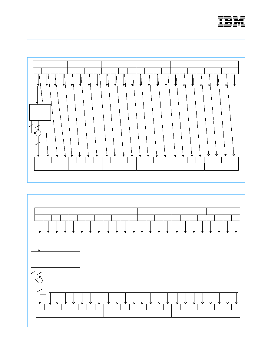
IBM PowerNP NP4GS3
Network Processor
Preliminary
Tree Search Engine
Page 374 of 605
np3_ds_sec08_tree.fm.11
January 29, 2003
Figure 8-19. 8-bit Hash Function
Figure 8-20. 12-bit Hash Function
B0
A0
K0 (bits 191..160)
D0
C0
B4
A4
K4 (bits 63..32)
D4
C4
B5
A5
K5 (bits 31..0)
D5
C5
B1
A1
K1 (bits 159..128)
D1
C1
B2
A2
K2 (bits 127..96)
D2
C2
B3
A3
K3 (bits 95..64)
D3
C3
A0
H0 (bits 191..160)
D0
C0
B4
A4
H4 (bits 63..32)
D4
C4
B5
A5
H5 (bits 31..0)
D5
C5
B1
A1
H1 (bits 159..128)
D1
C1
B2
A2
H2 (bits 127..96)
D2
C2
B3
A3
H3 (bits 95..64)
D3
C3
B0
IBM NP
8
8
8
IP 192
Bit Hasher
Note: Effective Hashed Key will be longer by 8 bits and Maximum Key length allowed is 184 bits with no color.
B0
A0
K0 (bits 191..160)
D0
C0
B4
A4
K4 (bits 63..32)
D4
C4
B5
A5
K5 (bits 31..0)
D5
C5
B1
A1
K1 (bits 159..128)
D1
C1
B2
A2
K2 (bits 127..96)
D2
C2
B3
A3
K3 (bits 95..64)
D3
C3
A0
H0 (bits 191..160)
D0
C0
B4
A4
H4 (bits 63..32)
D4
C4
B5
A5
H5 (bits 31..0)
D5
C5
B1
A1
H1 (bits 159..128)
D1
C1
B2
A2
H2 (bits 127..96)
D2
C2
B3
A3
H3 (bits 95..64)
D3
C3
B0
IBM NP
12 12
12
IP 192 bit hasher
D5 = 00000000
C5 = xxxx0000
Note: Effective Hashed Key will be longer by 12 bits and Maximum Key length allowed is 180 bits with no color.

IBM PowerNP NP4GS3
Preliminary
Network Processor
np3_ds_sec08_tree.fm.11
January 29, 2003
Tree Search Engine
Page 375 of 605
Figure 8-21. 16 bit Hash Function
B0
A0
K0 (bits 191..160)
D0
C0
B4
A4
K4 (bits 63..32)
D4
C4
B5
A5
K5 (bits 31..0)
D5
C5
B1
A1
K1 (bits 159..128)
D1
C1
B2
A2
K2 (bits 127..96)
D2
C2
B3
A3
K3 (bits 95..64)
D3
C3
A0
H0 (bits 191..160)
D0
C0
B4
A4
H4 (bits 63..32)
D4
C4
B5
A5
H5 (bits 31..0)
D5
C5
B1
A1
H1 (bits 159..128)
D1
C1
B2
A2
H2 (bits 127..96)
D2
C2
B3
A3
H3 (bits 95..64)
D3
C3
B0
IBM NP
IP 192 bit hasher
D5 = 00000000
C5 = 00000000
B0
A0
D0
C0
B4
A4
D4
C4
B5
A5
B1
A1
D1
C1
B2
A2
D2
C2
B3
A3
D3
C3
Note: Effective Hashed Key will be longer by 16 bits and Maximum Key length allowed is 176 bits with no color.
8
8

IBM PowerNP NP4GS3
Network Processor
Preliminary
Tree Search Engine
Page 376 of 605
np3_ds_sec08_tree.fm.11
January 29, 2003
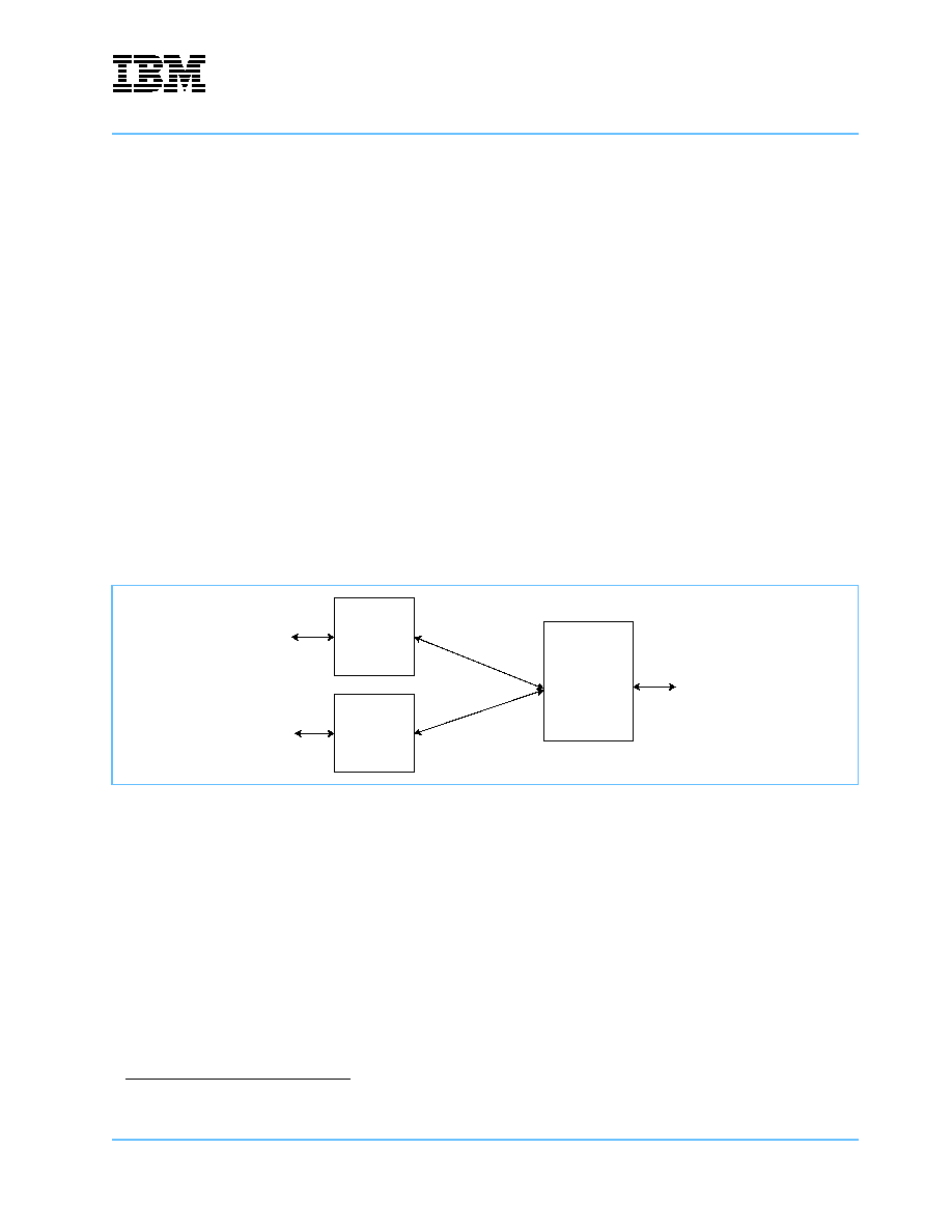
IBM PowerNP NP4GS3
Preliminary
Network Processor
np3_ds_sec09_spm.fm.11
January 29, 2003
Serial / Parallel Manager Interface
Page 377 of 605
9. Serial / Parallel Manager Interface
Located within the Embedded Processor Complex (EPC), the Serial / Parallel Manager (SPM) Interface is a
serial interface for communication with external devices. The SPM Interface consists of a clock signal output,
a bi-directional data signal, and an interrupt input. On this interface, the NP4GS3 is the master and the
external SPM module is the only slave
1
. The SPM Interface loads picocode, allowing management of phys-
ical layer devices (PHYs) and access to card-based functions such as light-emitting diodes (LEDs).
The SPM Interface supports:
� An external SPM module
� Boot code load via external SPM and EEPROM
� Boot override via CABWatch interface or Boot_Picocode configuration device I/O
� Access to external PHYs, LEDs, management, and card-based functions
9.1 SPM Interface Components
Figure 9-1 shows the functional blocks of the SPM Interface. The list following the figure describes them.
1.IBM does not supply the external SPM module.
Figure 9-1. SPM Interface Block Diagram
Boot State Machine
Starts up after reset if configured to do so by an external I/O pin (Boot_Picocode
set to 0). It selects one of two boot images (picocode loads) based on a configura-
tion flag found in the EEPROM and places the code into the instruction memory in
the EPC. Once the code is loaded, the Boot State Machine causes an interrupt that
starts up the Guided Frame Handler (GFH) thread, which executes the loaded
code.
CAB Interface
A memory mapped interface to the NP4GS3 that allows the protocol processors to
access any external device, including an SPM module, external PHYs, or card
LEDs.
Parallel to Serial
Control
Converts between the internal 32-bit read/write parallel interface and the 3-bit
external bi-directional serial interface.
Instruction
Memory
CAB
Boot State
Machine
CAB
Interface
Parallel to
Serial
Control
External SPM Module

IBM PowerNP NP4GS3
Network Processor
Preliminary
Serial / Parallel Manager Interface
Page 378 of 605
np3_ds_sec09_spm.fm.11
January 29, 2003
9.2 SPM Interface Data Flow
The SPM Interface is used initially to boot the NP4GS3. Following a reset, the SPM Interface reads an
external EEPROM and loads the EEPROM's contents into the EPC's Instruction Memory. When loading is
complete, the SPM Interface causes a POR interrupt that causes the Guided Frame Handler (GFH) to start
executing the boot code. The boot code initializes the network processor's internal structures and configures
all the interfaces that the network processor requires to operate. When all boot processing is complete, the
GFH activates the operational signal to indicate its availability to the control point function (CPF). The CPF
sends guided frames to further initialize and configure the network processor, preparing it for network opera-
tion.
The Boot State Machine supports two images of boot code in external EEPROM (see Figure 9-2). The
contents of byte x'0 0000' in EEPROM is examined during the read process to determine which image to
load. When the most significant bit of this byte is a `0', the current image resides at addresses x`0 0001' -
x`0 4000'. Otherwise, the current image resides at addresses x`1 0001' - x`1 4000'. The Boot State Machine
will load the appropriate image and allow the other image area to be used for boot code updates.

IBM PowerNP NP4GS3
Preliminary
Network Processor
np3_ds_sec09_spm.fm.11
January 29, 2003
Serial / Parallel Manager Interface
Page 379 of 605
The SPM Interface is also used during initialization and statistics gathering. It interfaces with the Ethernet
PHYs, card LEDs, and other card-level structures through an external SPM interface module supplied by the
customer. These external structures are mapped to the Control Access Bus (CAB) address space and are
accessed from the picocode using the same methods as those used to access any internal data structures:
the picocode issues reads or writes to the appropriate address and the SPM Interface converts these reads
and writes to serial communications with the external SPM module. The external SPM module re-converts
these serial communications to register reads and writes and to access the desired card device. Through the
SPM interface, the picocode has indirect access to all card-level functions and can configure or gather statis-
tics from these devices as if they were directly attached to the CAB interface.
Figure 9-2. EPC Boot Image in External EEPROM
Boot Flag
DASL Picocode
x`0 0000'
x`0 0001'
x`0 4000'
Boot Code & POST & Boot GFH
7
0
x`0 4001'
16 K
8 K
x`0 6000'
x`0 6001'
POST Overflow & Extended POST
16 K
x`0 A000'
x`0 A001'
Other
24 K
Not Used
DASL Picocode
x`1 0000'
x`1 0001'
x`1 4000'
Boot Code & POST & Boot GFH
x`1 4001'
16 K
8 K
x`1 6000'
x`1 6001'
POST Overflow & Extended POST
16 K
x`1 A000'
x`1 A001'
Other
24 K
x`0 FFFF'
x`1 FFFF'
Image B
Image A

IBM PowerNP NP4GS3
Network Processor
Preliminary
Serial / Parallel Manager Interface
Page 380 of 605
np3_ds_sec09_spm.fm.11
January 29, 2003
9.3 SPM Interface Protocol
The SPM Interface operates synchronously with the 33-MHz clock signal output. Data, address, and control
information is transferred serially on a bidirectional data signal. Transitions on this data signal occur at the
rising edges of the clock signal. Each data exchange is initiated by the NP4GS3 and can be one to four bytes
in length. Figure 9-3 illustrates the timing of the SPM Interface.
For single-byte transfers, the exchange begins when the NP4GS3 drives the data signal to `1' for one clock
period. This "select" indication is followed by a 1-bit write/read indication, a 4-bit burst length indication, and a
25-bit address value.
For read and write transfers, the SPM Interface master waits for a response from the SPM Interface slave,
and the slave communicates with the master using the following acknowledgments:
� ack: a `1' driven onto the data bus by the SPM Interface slave to indicate each successful byte operation,
either read or write.
� ack: a `0' driven onto the data bus by the SPM Interface slave while the byte operation is in progress.
For write transfers (see Figure 9-4), the address is followed immediately by eight bits of data. The NP4GS3
puts its driver in High-Z mode. One clock period later, the slave drives the data signal to `0' (ack) until the byte
write operation is complete. The slave then drives the data signal to `1' (ack). During the byte write operation,
the NP4GS3 samples the data input looking for a `1' (ack). Immediately following the ack, the slave puts its
driver in High-Z mode. The transfer is concluded one clock period later.
Figure 9-3. SPM Bit Timing
Figure 9-4. SPM Interface Write Protocol
T
.25T
Clock
...
Data
.25T
.25T
...
sel write
...
...
idle
sel write
...
...
idle
r/w
...
One Byte Write
Two Byte Write (Burst Length = 0010)
...
r/w
...
...
...
zero or more acks
preceding one ack
new sequence
can begin here
bl3
bl0 a24
a0
d7
d0
TS �ack TS sel
bl3
bl0
a24
a0
d7
TS
TS
TS
TS
d0
�ack
start
d7
�ack
d0
sel
Note:
bl# = bit # of the burst length
a# = bit # of the address
�ack = acknowledgment
sel = select

IBM PowerNP NP4GS3
Preliminary
Network Processor
np3_ds_sec09_spm.fm.11
January 29, 2003
Serial / Parallel Manager Interface
Page 381 of 605
For read transfers (see Figure 9-5), the address is followed by the NP4GS3 putting its driver into High-Z
mode. One clock period later, the slave drives the data signal to `0' (ack) until the byte of read data is ready
for transfer. The slave then drives the data signal to `1' (ack). During this time, the NP4GS3 samples the data
input looking for an ack. Immediately following the ack, the slave drives the eight bits of data onto the data
signal and then puts its driver in High-Z mode. The transfer is concluded one clock period later.
The protocol for multiple byte transfers is similar, except that each byte written is accompanied by a bus turn-
around, zero or more acks, and an ack. Read bursts are characterized by the slave retaining bus ownership
until the last byte of the burst is transferred. Each successive byte read is preceded by at least one `0' on the
data bus followed by one `1' on the data bus (ack), and immediately followed by the eight bits of data.
Figure 9-5. SPM Interface Read Protocol
read
sel
...
...
idle
...
r/w
read
sel
...
...
idle
...
...
...
r/w
...
One Byte Read
Two Byte Read (Burst Length = 0010)
one or more acks
preceding one ack
zero or more acks
preceding one ack
new sequence
can begin here
bl3
bl0
a24
a0
TS
�ack
d7
d0
TS
sel
bl3
bl0
a24
a0
�ack
TS
d7
d0
�ack
d0
TS
sel
Note:
bl# = bit # of the burst length
a# = bit # of the address
�ack = acknowledgment
sel = select
d7
IBM PowerNP NP4GS3
Network Processor
Preliminary
Serial / Parallel Manager Interface
Page 382 of 605
np3_ds_sec09_spm.fm.11
January 29, 2003
9.4 SPM CAB Address Space
The SPM Interface enables the control access bus (CAB) to access an external EEPROM and other devices
attached via an external SPM module developed by the customer. The address space is divided into three
areas:
� Byte access
� Word access
� EEPROM access
9.4.1 Byte Access Space
All elements accessed in byte access space are limited to a single byte in width.
9.4.2 Word Access Space
All elements accessed in word access space are a word in width.
Access Type
R/W
Base Addresses
x`2800 0000' through x`281F FFFF'
x`2880 0000' through x`28FF FFFF'
Byte Data
Reserved
31 30 29 28 27 26 25 24 23 22 21 20 19 18 17 16 15 14 13 12 11 10
9
8
7
6
5
4
3
2
1
0
Field Name
Bit(s)
Reset
Description
Byte Data
31:24
Data at this location
Reserved
23:0
Reserved
Access Type:
R/W
Base Addresses:
x`2820 0000' through x`287F FFFF'
Word Data
31 30 29 28 27 26 25 24 23 22 21 20 19 18 17 16 15 14 13 12 11 10
9
8
7
6
5
4
3
2
1
0
Field Name
Bit(s)
Reset
Description
Word Data
31:0
Data at this location

IBM PowerNP NP4GS3
Preliminary
Network Processor
np3_ds_sec09_spm.fm.11
January 29, 2003
Serial / Parallel Manager Interface
Page 383 of 605
9.4.3 EEPROM Access Space
The SPM Interface and a customer-supplied external SPM module can be combined to provide access to an
attached EEPROM. The EEPROM access space contains locations for 16 M 1-byte elements. All write
accesses are limited to a single byte, but read accesses may be in bursts of 1, 2, 3, or 4 bytes. The CAB
address is formed using the field definitions shown in Table 9-1.
9.4.3.1 EEPROM Single-Byte Access
Addresses in this space are used for single-byte read or write access to the EEPROM.
Table 9-1. Field Definitions for CAB Addresses
Bits Description
31:27
`00101'
26:25
Encoded burst length
00
4-byte burst (read only)
01
1-byte burst (read or write)
10
2-byte burst (read only)
11
3-byte burst (read only)
24
`1'
23:0
Starting Byte address for read or write action
Access Type:
R/W
Base Addresses:
x`2B00 0000' through x`2BFF FFFF'
Byte Data
Reserved
31 30 29 28 27 26 25 24 23 22 21 20 19 18 17 16 15 14 13 12 11 10
9
8
7
6
5
4
3
2
1
0
Field Name
Bit(s)
Reset
Description
Byte Data
31:24
Data at starting byte address
Reserved
23:0
Reserved
IBM PowerNP NP4GS3
Network Processor
Preliminary
Serial / Parallel Manager Interface
Page 384 of 605
np3_ds_sec09_spm.fm.11
January 29, 2003
9.4.3.2 EEPROM 2-Byte Access
Addresses in this space are used for a 2-byte read burst access to the EEPROM.
9.4.3.3 EEPROM 3-Byte Access
Addresses in this space are used for a 3-byte read burst access to the EEPROM.
Access Type:
Read Only
Base Addresses:
x`2D00 0000' through x`2DFF FFFF'
Byte 0 Data
Byte 1 Data
Reserved
31 30 29 28 27 26 25 24 23 22 21 20 19 18 17 16 15 14 13 12 11 10
9
8
7
6
5
4
3
2
1
0
Field Name
Bit(s)
Reset
Description
Byte 0 Data
31:24
Data at starting byte address
Byte 1 Data
23:16
Data at starting byte address + 1
Reserved
15:0
Reserved
Access Type:
Read Only
Base Addresses:
x`2F00 0000' through x`2FFF FFFF'
Byte 0 Data
Byte 1 Data
Byte 2 Data
Reserved
31 30 29 28 27 26 25 24 23 22 21 20 19 18 17 16 15 14 13 12 11 10
9
8
7
6
5
4
3
2
1
0
Field Name
Bit(s)
Reset
Description
Byte 0 Data
31:24
Data at byte address
Byte 1 Data
23:16
Data at byte address + 1
Byte 2 Data
15:8
Data byte address + 2
Reserved
7:0
Reserved
IBM PowerNP NP4GS3
Preliminary
Network Processor
np3_ds_sec09_spm.fm.11
January 29, 2003
Serial / Parallel Manager Interface
Page 385 of 605
9.4.3.4 EEPROM 4-Byte Access
Addresses in this space are used for a 4-byte read burst access to the EEPROM.
Access Type:
Read only
Base Addresses:
x`2900 0000' through x`29FF FFFF'
Byte 0 Data
Byte 1 Data
Byte 2 Data
Byte 3 Data
31 30 29 28 27 26 25 24 23 22 21 20 19 18 17 16 15 14 13 12 11 10
9
8
7
6
5
4
3
2
1
0
Field Name
Bit(s)
Reset
Description
Byte 0 Data
31:24
Data at byte address
Byte 1 Data
23:16
Data at byte address + 1
Byte 2 Data
15:8
Data byte address + 2
Byte 3 Data
7:0
Data byte address + 3

IBM PowerNP NP4GS3
Network Processor
Preliminary
Serial / Parallel Manager Interface
Page 386 of 605
np3_ds_sec09_spm.fm.11
January 29, 2003

IBM PowerNP NP4GS3
Preliminary
Network Processor
np3_ds_sec10_eppc.fm.11
January 29, 2003
Embedded PowerPCTM Subsystem
Page 387 of 605
10. Embedded PowerPCTM Subsystem
10.1 Description
The IBM PowerNP NP4GS3 incorporates an embedded PowerPC subsystem. This subsystem consists of
mixture of macros from IBM's PowerPC macro library and other components that were designed specifically
for the NP4GS3.
Standard IBM PowerPC macros include the following:
� 133 MHz PPC405 Processor Core with 16 K of instruction cache and 16 K of data cache
� NP4GS3B (R2.0) uses the PPC405D4V4 core
� NP4GS3C (R3.x) uses the PPC405D4V6 core
� 133 MHz, 64-bit PLB macro with PLB arbiter
� 33/66 MHz, 32-bit PCI to 133 MHz, 64-bit PLB macro
� PowerPC Universal Interrupt Controller (UIC) macro
Documentation for the above macros is contained in the IBM PowerPC 405GP Embedded Processor User's
Manual (
http://www-3.ibm.com/chips/techlib/techlib.nsf/products/PowerPC_405GP_Embedded_Processor
)
and is not repeated here. That document also contains information for other macro library components not
contained in the NP4GS3 which does not apply to the above macros.
The embedded PowerPC subsystem includes a CAB Interface PLB slave unit to access NP4GS3 internal
structures and a Mailbox and DRAM Interface PLB slave unit for inter-processor communications and access
to PowerPC instructions.
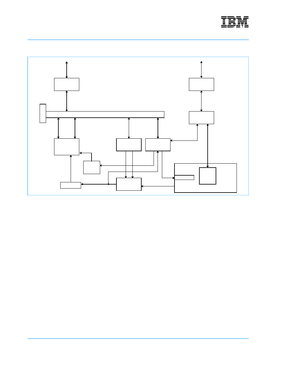
IBM PowerNP NP4GS3
Network Processor
Preliminary
Embedded PowerPCTM Subsystem
Page 388 of 605
np3_ds_sec10_eppc.fm.11
January 29, 2003
Figure 10-1. PowerPC Subsystem Block Diagram
PowerPC
64-bit PLB
Arbiter
PCI/PLB
Mailbox &
EPC
GPH
Reset Cntl
To DRAM
To PCI Bus
CAB
405 Core
Interface
DRAM I/F
Macro
DRAM
Controller
DRAM
Arbiter
CAB
Arbiter
CAB
Interrupts
Universal
Interrupt
Controller

IBM PowerNP NP4GS3
Preliminary
Network Processor
np3_ds_sec10_eppc.fm.11
January 29, 2003
Embedded PowerPCTM Subsystem
Page 389 of 605
10.2 Processor Local Bus and Device Control Register Buses
The on-chip bus structure consisting of the Processor Local Bus (PLB) and the Device Control Register bus
(DCR) provides a link between the processor core and the other peripherals (PLB master and slave devices)
used in PowerPC subsystem design.
10.2.1 Processor Local Bus (PLB)
The PLB is the high performance bus used to access memory, PCI devices, and NP4GS3 structures through
the PLB interface units. The PLB interface units shown in Figure 10-1, the CAB Interface and the Mailbox &
DRAM interface, are PLB slaves. The processor core has two PLB master connections, one for instruction
cache and one for data cache. The PCI to PLB interface unit, which is both a PLB master and PLB slave
device, is also attached to the PLB. The PLB master corresponds to the PCI target and the PLB slave corre-
sponds to the PCI master.
Each PLB master is attached to the PLB through separate address, read data, and write data buses and a
plurality of transfer qualifier signals. PLB slaves are attached to the PLB through shared, but decoupled,
address, read data, and write data buses and a plurality of transfer control and status signals for each data
bus.
Access to the PLB is granted through a central arbitration mechanism that allows masters to compete for bus
ownership. This mechanism is flexible enough to provide for the implementation of various priority schemes.
Additionally, an arbitration locking mechanism is provided to support master-driven atomic operations.
The PLB is a fully-synchronous bus. Timing for all PLB signals is provided by a single clock source that is
shared by all masters and slaves attached to the PLB.
Table 10-1. PLB Master Connections
Master ID
Master Unit Description
0
Processor Core Instruction Cache Unit
1
Processor Core Data Cache Unit
2
PLB/PCI Macro Unit
Others
Unused

IBM PowerNP NP4GS3
Network Processor
Preliminary
Embedded PowerPCTM Subsystem
Page 390 of 605
np3_ds_sec10_eppc.fm.11
January 29, 2003
10.2.2 Device Control Register (DCR) Bus
The Device Control Register (DCR) bus is used primarily to access status and control registers within the
PLB and the Universal Interrupt Controller (UIC). The DCR bus architecture allows data transfers among
peripherals to occur independently from, and concurrent with, data transfers between the processor and
memory or among other PLB devices.
All PLB arbiter registers and Universal Interrupt Controller registers are device control registers. They are
accessed by using the Move From Device Control Register (mfdcr) and Move To Device Control Register
(mtdcr) instructions. PLB arbiter registers are architected as 32-bits and are privileged for both read and write.
The DCR base address of the PLB registers is x'080'. The DCR base address of the UIC registers is x'0C0'.
Details regarding the PLB and UIC device control registers can be found in the IBM PowerPC 405GP
Embedded Processor User's Manual (
http://www-3.ibm.com/chips/techlib/techlib.nsf/products/
PowerPC_405GP_Embedded_Processor
).
Table 10-2. Device Control Registers
Register
DCR Offset
Description
Access
Processor Local Bus Arbiter Macro
REV
x`02'
PLB Arbiter Revision ID
R
BESR
x`04'
PLB Bus Error Status Register
R/Clear
BEAR
x`06'
PLB Bus Error Address Register
R
ACR
x`07'
PLB Arbiter Control Register
R/W
Universal Interrupt Controller Macro
SR
x`00'
UIC Status Register
R/Clear
SRS
x`01'
UIC Status Register Set
R/Set
ER
x`02'
UIC Enable Register
R/W
CR
x`03'
UIC Critical Register
R/W
PR
x`04'
UIC Polarity Register
R/W
TR
x`05'
UIC Triggering Register
R/W
MSR
x`06'
UIC Masked Status Register
R
VR
x`07'
UIC Vector Register
R
VCR
x`08'
UIC Vector Configuration Register
W

IBM PowerNP NP4GS3
Preliminary
Network Processor
np3_ds_sec10_eppc.fm.11
January 29, 2003
Embedded PowerPCTM Subsystem
Page 391 of 605
10.3 PLB Address Map
Components of the embedded PowerPC subsystem are connected using the Processor Local Bus (PLB).
These components recognize PLB address values as their own. These PLB address values are fixed by
hardware. The PLB address map describes the association of PLB address values and the components that
recognize them.
Table 10-3. Address Map for CAB Interface Macro
Symbolic Address
PLB Address
Description
Access
PwrPC_CAB_Addr
x`7800 0000'
PowerPC CAB Address Register
R/W
PwrPC_CAB_Data
x`7800 0008'
PowerPC CAB Data Register
R/W
PwrPC_CAB_Cntl
x`7800 0010'
PowerPC CAB Control Register
R/W
1
PwrPC_CAB_Status
x`7800 0018'
PowerPC CAB Status Register
R
PwrPC_CAB_Mask
x'7800 0020'
PowerPC CAB Mask Register
R/W
PwrPC_CAB_WUM_Data
x'7800 0028'
PowerPC CAB Write Under Mask Data Register
W
Host_CAB_Addr
x`7800 8000'
PCI Host CAB Address Register
R/W
Host_CAB_Data
x`7800 8008'
PCI Host CAB Data Register
R/W
Host_CAB_Cntl
x`7800 8010'
PCI Host CAB Control Register
R/W
1
Host_CAB_Status
x`7800 8018'
PCI Host CAB Status Register
R
Host_CAB_Mask
x'7800 8020'
PCI Host CAB Mask Register
R/W
Host_CAB_WUM_Data
x'7800 8028'
PCI Host CAB Write Under Mask Data Register
W
Unassigned addresses in the range x`7801 0000' - x`7801 FFFF' are reserved.
1. Additional action occurs on register access using the specified address. Refer to register detailed section for more
information.
Table 10-4. PLB Address Map for Mailbox and DRAM Interface Macro
(Page 1 of 2)
Symbolic Address
PLB Address
Description
Access
PCI_Interr_Status
x`7801 0000'
PCI Interrupt Status Register
R
PCI_Interr_Ena
x`7801 0008'
PCI Interrupt Enable Register
R/W
P2H_Msg_Resource
x`7801 0010'
PowerPC Subsystem to PCI Host Resource Register
R/W
1
P2H_Msg_Addr
x`7801 0018'
PowerPC Subsystem to PCI Host Message Address Register
R/W
1
P2H_Doorbell
x`7801 0020'
PowerPC Subsystem to PCI Host Doorbell Register (PowerPC Access)
R/SUM
x`7801 0028'
PowerPC Subsystem to PCI Host Doorbell Register (PCI Host Access)
R/RUM
H2P_Msg_Addr
x`7801 0050'
PCI Host to PowerPC Subsystem Message Address Register (Reset Status)
R
1
x`7801 0060'
PCI Host to PowerPC Subsystem Message Address Register
R/W
1
H2P_Doorbell
x`7801 0030'
PCI Host to PowerPC Subsystem Doorbell Register (PCI Host Access)
R/SUM
x`7801 0038'
PCI Host to PowerPC Doorbell Register (PowerPC Access)
R/RUM
E2P_Msg_Resource
x`7801 0040'
EPC to PowerPC Subsystem Message Resource Register
R/W
Unassigned addresses in the range x`7801 0000' - x`7801 FFFF' are reserved
1. Additional action occurs on register access using the specified address. Refer to register detailed section for more
information.

IBM PowerNP NP4GS3
Network Processor
Preliminary
Embedded PowerPCTM Subsystem
Page 392 of 605
np3_ds_sec10_eppc.fm.11
January 29, 2003
E2P_Msg_Addr
x`7801 0048'
EPC to PowerPC Subsystem Message Address Register
R
1
E2P_Doorbell
x`7801 0058'
EPC to PowerPC Subsystem Doorbell Register (PowerPC Access)
R/RUM
P2E_Msg_Addr
x`7801 0068'
PowerPC Subsystem to EPC Message Address Register
R/W
P2E_Doorbell
x`7801 0070'
PowerPC Subsystem to EPC Doorbell Register (PowerPC Access)
R/SUM
E2H_Msg_Resource
x`7801 0080'
EPC to PCI Host Message Resource Register
R/W
E2H_Msg_Addr
x`7801 0088'
EPC to PCI Host Message Address Register
R
1
E2H_Doorbell
x`7801 0098'
EPC to PCI Host Doorbell Register (PCI Host Access)
R/RUM
H2E_Msg_Addr
x`7801 00A8'
PCI Host to EPC Message Address Register
R/W
Msg_Status
x`7801 00A0'
Message Status Register
R
H2E_Doorbell
x`7801 00B0'
PCI Host to EPC Doorbell Register (PCI Host Access)
R/SUM
SEAR
x'7801 00B8'
Slave Error Address Register
R
SESR
x'7801 00C0'
Slave Error Status Register
RWR
1
Perr_Cntr
x'7801 00C8'
Parity Error Counter Register
R
PwrPC_Inst_Store
x`0000 0000' -
x`07FF FFFF'
PowerPC Instruction/Data DRAM
R/W
Table 10-4. PLB Address Map for Mailbox and DRAM Interface Macro
(Page 2 of 2)
Symbolic Address
PLB Address
Description
Access
Unassigned addresses in the range x`7801 0000' - x`7801 FFFF' are reserved
1. Additional action occurs on register access using the specified address. Refer to register detailed section for more
information.

IBM PowerNP NP4GS3
Preliminary
Network Processor
np3_ds_sec10_eppc.fm.11
January 29, 2003
Embedded PowerPCTM Subsystem
Page 393 of 605
10.4 CAB Address Map
Some components of the embedded PowerPC subsystem
are also accessible via the NP4GS3's CAB Inter-
face. These components are accessed using CAB addresses as shown in the CAB Address Map.
Table 10-5. CAB Address Map for Mailbox and DRAM Interface Macro
Symbolic Address
CAB Address
Description
Access
Boot_Redir_Inst
x`3800 0110'
-
x`3800 0117'
Boot Redirection Instruction Registers for instruction addresses
x`FFFF FFE0' - x`FFFF FFFC'
R/W
PwrPC_Mach_Chk
x`3800 0210'
PowerPC Subsystem Machine Check Register
R
E2P_Msg_Resource
x`3801 0010
'
EPC to PowerPC Subsystem Message Resource Register
R
1
E2P_Msg_Addr
x`3801 0020'
EPC to PowerPC Subsystem Message Address Register
R/W
E2P_Doorbell
x`3801 0040'
EPC to PowerPC Doorbell Register (PowerPC Access)
R/SUM
P2E_Msg_Addr
x`3801 0080'
PowerPC Subsystem to EPC Message Address Register
R
x`3802 0010'
PowerPC Subsystem to EPC Message Address Register
R
1
P2E_Doorbell
x`3801 0100'
PowerPC Subsystem to EPC Doorbell Register (PowerPC Access)
R/RUM
E2H_Msg_Resource
x`3801 0200'
EPC to PCI Host Message Resource Register
R
1
E2H_Msg_Addr
x`3801 0400'
EPC to PCI Host Message Address Register
R/W
E2H_Doorbell
x`3801 0800'
EPC to PCI Host Doorbell Register (PCI Host Access)
R/SUM
H2E_Msg_Addr
x`3801 1000'
PCI Host to EPC Message Address Register
R
1
x`3802 0020'
PCI Host to EPC Message Address Register
R
1
H2E_Doorbell
x`3801 2000'
PCI Host to EPC Doorbell Register (PCI Host Access)
R/RUM
Msg_Status
x`3801 4000'
Message Status Register
R
1. Additional action occurs on register access using the specified address. Refer to register detailed section for more
information.

IBM PowerNP NP4GS3
Network Processor
Preliminary
Embedded PowerPCTM Subsystem
Page 394 of 605
np3_ds_sec10_eppc.fm.11
January 29, 2003
10.5 Universal Interrupt Controller (UIC) Macro
The Universal Interrupt Controller (UIC) provides all the necessary control, status, and communication
between the various of interrupts sources and the microprocessor core. The UIC supports six on-chip and two
external sources of interrupts. Status reporting (using the UIC Status Register (UICSR)) is provided to ensure
that systems software can determine the current and interrupting state of the system and respond appropri-
ately. Software can generate interrupts to simplify software development and for diagnostics.
The interrupts can be programmed, using the UIC Critical Register (UICCR), to generate either a critical or a
non-critical interrupt signal.
The UIC supports internal and external interrupt sources as defined in Table 10-6.
The on-chip interrupts (interrupts 0, and 3-7) and the external interrupts (interrupts 1-2) are programmable.
However, the on-chip interrupts must be programmed as shown in Table 10-6. For details regarding the
control of the UIC, including the programming of interrupts, see the IBM PowerPC 405GP Embedded
Processor User's Manual (
http://www-3.ibm.com/chips/techlib/techlib.nsf/products/
PowerPC_405GP_Embedded_Processor
Table 10-6. UIC Interrupt Assignments
Interrupt
Polarity
Sensitivity
Interrupt Source
0
High
Edge
DRAM D6 Parity Error
1
Programmable
Programmable
External Interrupt 0 (PCI_Bus_NM_Int input pin)
2
Programmable
Programmable
External Interrupt 1 (PCI_Bus_M_Int input pin)
3
High
Level
PCI Host to PowerPC Doorbell Interrupt
4
High
Level
PCI Host to PowerPC Message Interrupt
5
High
Level
Embedded Processor Complex to PowerPC Doorbell Interrupt
6
High
Level
Embedded Processor Complex to PowerPC Message Interrupt
7
High
Level
PCI Command Write Interrupt generated when an external PCI master
writes to the PCI Command Register or bit 13 of the Bridge Options 2
Register is set to `1' via PCI configuration. See description of the PCI
macro's Bridge Options 2 Register in the PPC405GP Embedded Control-
ler User's Manual for details.
8-31
High
Level
unused, interrupt input to UIC tied low.

IBM PowerNP NP4GS3
Preliminary
Network Processor
np3_ds_sec10_eppc.fm.11
January 29, 2003
Embedded PowerPCTM Subsystem
Page 395 of 605
10.6 PCI/PLB Bridge Macro
The Peripheral Component Interconnect (PCI) interface controller provides an interface for connecting PLB-
compliant devices to PCI devices. The controller complies with PCI Specification, version 2.2. (
http://
www.pcisig.com
).
Values of the PCI Device Configuration Header for the NP4GS3 are initialized by hardware. These values are
shown in Table 10-7. When the boot picocode is loaded from the Management Bus (Boot_Picocode is tied
to `0') and the PowerPC subsystem boots from DRAM D6 (Boot_PPC is tied to `0', see 2.1.8 Miscellaneous
Pins on page 79), a general reset initializes the PCI/PLB macro's Bridge Options 2 Register
(PCIBRDGOPT2) with its Host Configuration Enable bit set to `0' (disabled). This allows the PowerPC
subsystem to alter the contents of the PCI Device Configuration Header registers prior to access by external
configuration. The PowerPC code then enables external host configuration.
The PCI/PLB macro responds as a target on the PLB bus in several address ranges. These ranges allow a
PLB master to configure the PCI/PLB macro, and to cause the PCI/PLB macro to generate memory, I/O,
configuration, interrupt acknowledge, and special cycles to the PCI bus. Table 10-8 shows the address map
from the view of the PLB, that is, as decoded by the PCI/PLB macro as a PLB slave.
Table 10-7. NP4GS3 PCI Device Configuration Header Values
Register Name
Register Value
Vendor ID
x'1014'
Device ID
x'01E8'
Revision ID
x'00'
Class Code
x'028000'
Subsystem ID
x'0000"
Subsystem Vendor ID
x'0000'
Table 10-8. PLB Address Map for PCI/PLB Macro
(Page 1 of 2)
PLB Address Range
Description
PCI Address Range
x`E800 0000' - x`E800 FFFF'
PCI I/O
Accesses to this range are translated to an I/O access on PCI in the
range 0 to 64 KB - 1
x`0000 0000' - x`0000 FFFF' (I/O)
x`E801 0000 x`E87F FFFF`
Reserved
PCI/PLB Macro does not respond (Other bridges use this space for
non-contiguous I/O).
x`E880 0000' -
x`EBFF FFFF'
PCI I/O
Accesses to this range are translated to an I/O access on PCI in the
range 8 MB to 64 MB - 1
x`0080 0000' - x`03FF FFFF' (I/O)
x`EC00 0000' -
x`EEBF FFFF'
Reserved
PCI/PLB Macro does not respond
x`EEC0 0000' -
x`EECF FFFF'
PCI Configuration Address and Data
x`EEC0 0000': PCICFGADDR
x`EEC0 0004': PCICFGDATA
x`EEC0 0008' - x`EECF FFFF': Reserved (can mirror PCICFGDATA)

IBM PowerNP NP4GS3
Network Processor
Preliminary
Embedded PowerPCTM Subsystem
Page 396 of 605
np3_ds_sec10_eppc.fm.11
January 29, 2003
Following a general reset of the NP4GS3, the PCI Target Map 1 is enabled for a PCI address range of 128
KB and is mapped to the PLB address range of x'7800 0000 to x`7801 FFFF'. The corresponding PCI base
address for this range must be set by PCI configuration of the PCI PTM1 Base Address Register. Likewise,
the PCI Target Map 2 is enabled for a PCI address range of 128 MB and is mapped to the PLB address range
of x'0000 0000 to x`07FF FFFF'. The corresponding PCI base address for this range must be set by PCI
configuration of the PCI PTM2 Base Address Register.
The PCI/PLB macro has a mode that enables a PLB master to access a PCI memory range without initial
configuration cycles. This mode is enabled by strapping the boot_ppc input pin high. System designers, for
instance, may use this mode to allow a processor to access a boot ROM in PCI memory space. In this mode
x`EED0 0000' -
x`EEDF FFFF`
PCI Interrupt Acknowledge and Special Cycle
x`EED0 0000' read: Interrupt Acknowledge
x`EED0 0000' write: Special Cycle
x`EED0 0004' - x`EEDF FFFF': Reserved (can mirror Interrupt
Acknowledge and Special Cycle)
x`EEE0 0000' -
x`EF3F FFFF'
Reserved.
PCI/PLB Macro does not respond.
x`EF40 0000' - x`EF4F FFFF'
PCI/PLB Macro Local Configuration Registers
x`EF40 0000': PMM0LA
x`EF40 0004': PMM0MA
x`EF40 0008': PMM0PCILA
x`EF40 000C': PMM0PCIHA
x`EF40 0010': PMM1LA
x`EF40 0014': PMM1MA
x`EF40 0018': PMM1PCILA
x`EF40 001C': PMM1PCIHA
x`EF40 0020': PMM2LA
x`EF40 0024': PMM2MA
x`EF40 0028': PMM2PCILA
x`EF40 002C': PMM2PCIHA
x`EF40 0030': PTM1MS
x`EF40 0034': PTM1LA
x`EF40 0038': PTM2MS
x`EF40 003C': PTM2LA
x`F400 0400' - x`EF4F FFFF': Reserved (can mirror PCI local regis-
ters)
x`0000 0000' - x`FFFF FFFF'
PCI Memory - Range 0
PMM 0 registers map a region in PLB space to a region in PCI mem-
ory space. The address ranges are fully programmable. The PCI
address is 64 bits.
x`0000 0000 0000 0000'
x`FFFF FFFF FFFF FFFF'
x`0000 0000' - x`FFFF FFFF'
PCI Memory - Range 1
PMM 1 registers map a region in PLB space to a region in PCI mem-
ory space. The address ranges are fully programmable. The PCI
address is 64 bits.
x`0000 0000 0000 0000'
x`FFFF FFFF FFFF FFFF'
x`0000 0000' - x`FFFF FFFF'
PCI Memory - Range 2
PMM 2 registers map a region in PLB space to a region in PCI mem-
ory space. The address ranges are fully programmable. The PCI
address is 64 bits.
x`0000 0000 0000 0000'
x`FFFF FFFF FFFF FFFF'
Table 10-8. PLB Address Map for PCI/PLB Macro
(Page 2 of 2)
PLB Address Range
Description
PCI Address Range

IBM PowerNP NP4GS3
Preliminary
Network Processor
np3_ds_sec10_eppc.fm.11
January 29, 2003
Embedded PowerPCTM Subsystem
Page 397 of 605
the PCI/PLB macro comes out of reset with PMM0 enabled and programmed for the address range
x'FFFE 0000' - x'FFFF FFFF'. The ME field of the PCI Command register (PCICMD[ME]) is also set to 1 after
reset. Enabling PCI boot mode does not prevent subsequent updates to the PMM0 registers.
Unless the boot picocode is loaded from the SPM (Boot_Picocode tied to `0') and the PowerPC subsystem
boots from DRAM D6 (Boot_PPC tied to `0'), a general reset initializes the PCI/PLB macro's Bridge Options 2
Register (PCIBRDGOPT2) with its Host Configuration Enable bit set to `1' (enabled). This allows an external
source to access the PCI/PLB macro's configuration registers. Otherwise, PowerPC code must enable
external host configuration and may alter the contents of the PCI Device Configuration Header registers prior
to enabling external host configuration.
Table 10-9. PCI/PLB Bridge Macro Configuration Registers
(Page 1 of 2)
Register
Offset
Description
Access
Local
Host
VENDID
x`01' - x`00'
PCI Vendor ID
R/W
R
DEVID
x`03' - x`02'
PCI Device ID
R/W
R
CMD
x`05' - x`04'
PCI Command Register
R/W
R/W
STATUS
x`07' - x`06'
PCI Status Register
R/W
R/W
REVID
x`08'
PCI Revision ID
R/W
R
CLS
x`0B' - x`09'
PCI Class Register
R/W
R
CACHELS
x`0C'
PCI Cache Line Size
R
R
LATTIM
x`0D'
PCI Latency Timer
R/W
R/W
HDTYPE
x`0E'
PCI Header Type
R
R
BIST
x`0F'
PCI Built in Self Test Control
R
R
PTM1BAR
x`17' - x`14'
PCI PTM 1 BAR
R/W
R/W
PTM2BAR
x`1B' - x`18'
PCI PTM 2 BAR
R/W
R/W
SBSYSVID
x`2D' - x`2C'
PCI Subsystem Vendor ID
R/W
R
SBSYSID
x`2F' - x`2E'
PCI Subsystem ID
R/W
R
CAP
x`34'
PCI Capabilities Pointer
R
R
INTLN
x`3C'
PCI Interrupt Line
R/W
R/W
INTPN
x`3D'
PCI Interrupt Pin
R
R
MINGNT
x`3E'
PCI Minimum Grant
R
R
MAXLTNCY
x`3F'
PCI Maximum Latency
R
R
ICS
x`44'
PCI Interrupt Control/Status
R/W
R/W
ERREN
x`48'
Error Enable
R/W
R/W
ERRSTS
x`49'
Error Status
R/W
R/W
BRDGOPT1
x`4B' - x`4A'
PCI Bridge Options 1
R/W
R/W
PLBBESR0
x`4F' - x`4C'
PCI Slave Error Syndrome 0
R/W
R/W
PLBBESR1
x`53' - x`50'
PCI Slave Error Syndrome 1
R/W
R/W
PLBBEAR
x`57' - x`54'
PCI Slave Error Address Register
R
R
CAPID
x`58'
Capability Identifier
R
R

IBM PowerNP NP4GS3
Network Processor
Preliminary
Embedded PowerPCTM Subsystem
Page 398 of 605
np3_ds_sec10_eppc.fm.11
January 29, 2003
For further details regarding the PCI/PLB macro's control and configuration registers, see the IBM PowerPC
405GP Embedded Processor User's Manual (
http://www-3.ibm.com/chips/techlib/techlib.nsf/products/
PowerPC_405GP_Embedded_Processor
).
NEXTIPTR
x`59'
Next Item Pointer
R
R
PMC
x`5B' - x`5A'
Power Management Capabilities
R
R
PMCSR
x`5D' - x`5C'
Power Management Control Status
R/W
R/W
PMCSRBSE
x`5E'
PMCSR PCI to PCI Bridge Support Extensions
R
R
DATA
x`5F'
Data
R
R
BRDGOPT2
x`63' - x`60'
PCI Bridge Options 2
R/W
R/W
PMSCRR
x`64'
Power Management State Change Request Register
R/W
R/W
Table 10-9. PCI/PLB Bridge Macro Configuration Registers
(Page 2 of 2)
Register
Offset
Description
Access
Local
Host

IBM PowerNP NP4GS3
Preliminary
Network Processor
np3_ds_sec10_eppc.fm.11
January 29, 2003
Embedded PowerPCTM Subsystem
Page 399 of 605
10.7 CAB Interface Macro
The CAB Interface macro provides duplicate facilities to support independent CAB access of IBM Network
Processor control and status facilities by the PCI Host processor and the embedded PowerPC subsystem.
Exclusive access to these facilities, if required, is enforced through software discipline.
The PCI Host Processor can access the IBM Network Processor's CAB Interface through the following mech-
anism: after PCI configuration, one or more ranges of PCI addresses are mapped to PLB addresses.
Accessing these PCI addresses also accesses PowerPC PLB resources, which include the following CAB
interface registers:
� CAB Address register is set to the value of the CAB address to be read or written.
� CAB Control register is written with parameters that control the behavior for CAB access.
� CAB Data register, when accessed, initiates a CAB access and determines its type (read or write). If the
CAB Data register is written, then the CAB access will be a write access. Likewise reading the CAB Data
register will result in a CAB read access.
� Status register is read to determine, for polled access, whether read data is ready (rd_rdy).
The CAB Control register (w/p) controls the two modes of PLB protocol for CAB access:
� Wait access, w/p = `1', causes the CAB Interface macro to insert wait states on the PLB until the CAB
access is complete. Software need not read the CAB Status register to determine completion.
� CAB access in polled mode requires software to follow the protocol defined in Figure 10-2: Polled Access
Flow Diagram on page 400. Behavior for CAB accesses not following this protocol is undefined and may
result in adverse effects. Polled access, w/p = `0' requires software to read the CAB Status register to
synchronize software with the hardware when performing a CAB transaction. A CAB read transaction
requires at least two read accesses to the CAB_Data register. An additional read access of the
CAB_Data register may be required if the software is not synchronized with the hardware. Software syn-
chronization is determined initially by reading the CAB_Status register. The software is not synchronized
when the rd_rdy status bit is set to `1'. Synchronization is achieved by reading the CAB_Data register and
discarding the result.
A subsequent read of the CAB Data register initiates a CAB read access from the CAB address con-
tained in the CAB Address register. The data returned as a result of this read of the CAB_Data register is
stale data and is discarded by software. Software must then perform a final read of the CAB_Data regis-
ter to acquire the data accessed on the CAB and return the CAB Interface to its starting state (rd_rdy =
`0').
The NP4GS3 causes subsequent accesses to the CAB interface registers to be retried until a pending
CAB access is complete. Prolonged locking of the CAB by the EPC will result in extended retries by the
PowerPC subsystem or PCI Host. Under these conditions, system hardware and software design must
be able to tolerate long periods of retry.

IBM PowerNP NP4GS3
Network Processor
Preliminary
Embedded PowerPCTM Subsystem
Page 400 of 605
np3_ds_sec10_eppc.fm.11
January 29, 2003
Figure 10-2. Polled Access Flow Diagram
Start
Read CAB_Status
Read CAB_Data
and discard results
Read CAB_Data
and discard results
Y
N
rd_rdy = 1
CAB
read or write
wr
rd
Read CAB_Data
(sets rd_rdy to `0')
Finish
Write CAB_Data
with data value
Rd_Rdy = `1'
Hardware/Software
Synchronization
Pending CAB Read
CAB I/F access retried
Pending CAB Write
CAB I/F access retried
IBM PowerNP NP4GS3
Preliminary
Network Processor
np3_ds_sec10_eppc.fm.11
January 29, 2003
Embedded PowerPCTM Subsystem
Page 401 of 605
10.7.1 PowerPC CAB Address (PwrPC_CAB_Addr) Register
The PowerPC CAB Address register is accessible from the PLB and supplies a CAB address value for
PowerPC subsystem access to NP4GS3 structures via the CAB Interface.
10.7.2 PowerPC CAB Data (PwrPC_CAB_Data) Register
The PowerPC CAB Data register is accessible from the PLB and contains the value of CAB data written or
read when the PowerPC subsystem accesses NP4GS3 structures via the CAB Interface. Writing to the
PwrPC_CAB_Data register has the side effect of initiating a write access on the CAB. The data value written
to the PwrPC_CAB_Data register is written to the CAB address contained in the PwrPC_CAB_Addr register.
When the PwrPC_CAB_Cntl register has been configured with its w/p bit set to `1' or if its w/p bit is set to `0'
and the rd_rdy bit of the PwrPC_CAB_Status register is set to `0', a read of the PwrPC_CAB_Data register
has the side effect of initiating a corresponding read access on the CAB. At the end of the CAB read access,
the data value indicated by the PwrPC_CAB_Addr register is stored in the PwrPC_CAB_Data register and
the rd_rdy bit of the PwrPC_CAB_Status register is set to '1. When the w/p bit set to `1', the data value is also
returned to the PLB. Otherwise, a subsequent read access of the PwrPC_CAB_Data register is required to
retrieve the data value.
Access Type
Read/Write
Base Address (PLB)
x`7800 0000'
PwrPC_CAB_Addr
0
1
2
3
4
5
6
7
8
9
10 11 12 13 14 15 16 17 18 19 20 21 22 23 24 25 26 27 28 29 30 31
Field Name
Bit(s)
Reset
Description
PwrPC_CAB_Addr
0:31
x'0000 0000'
CAB address value for PowerPC subsystem access to NP4GS3 structures
via the CAB Interface.
Access Type
Read/Write
Base Address (PLB)
x`7800 0008'
PwrPC_CAB_Data
0
1
2
3
4
5
6
7
8
9
10 11 12 13 14 15 16 17 18 19 20 21 22 23 24 25 26 27 28 29 30 31
Field Name
Bit(s)
Reset
Description
PwrPC_CAB_Data
0:31
x'0000 0000'
CAB data written or read when the PowerPC subsystem accesses
NP4GS3 structures via the CAB Interface.

IBM PowerNP NP4GS3
Network Processor
Preliminary
Embedded PowerPCTM Subsystem
Page 402 of 605
np3_ds_sec10_eppc.fm.11
January 29, 2003
10.7.3 PowerPC CAB Control (PwrPC_CAB_Cntl) Register
The PowerPC CAB Control register is accessible from the PLB and controls the CAB access protocol used by
the PowerPC subsystem. The bit in this register indicates whether the wait or polled protocol is used when
the PowerPC subsystem accesses CAB connected structures within the NP4GS3.
10.7.4 PowerPC CAB Status (PwrPC_CAB_Status) Register
The PowerPC CAB Status register is accessible from the PLB and monitors the status of PowerPC CAB
accesses. Bits within this register indicate the status of PowerPC subsystem accesses of CAB connected
structures within the NP4GS3.
Access Type
Read/Write
Base Address (PLB)
x`7800 0010'
Reserved
w/
p
0
1
2
3
4
5
6
7
8
9
10 11 12 13 14 15 16 17 18 19 20 21 22 23 24 25 26 27 28 29 30 31
Field Name
Bit(s)
Reset
Description
Reserved
0:30
Reserved
w/p
31
0
Wait or polled access control value
0
PowerPC subsystem polls the PwrPC_CAB_Status register to
determine when access is complete
1
CAB Interface macro inserts wait states on the PLB until the CAB
access is complete
Access Type
Read
Base Address (PLB)
x`7800 0018'
Reserved
R
d_Rdy
Re
s
e
rv
ed
0
1
2
3
4
5
6
7
8
9
10 11 12 13 14 15 16 17 18 19 20 21 22 23 24 25 26 27 28 29 30 31
Field Name
Bit(s)
Description
Reserved
0:29
Reserved
Rd_Rdy
30
Read Data Ready indicator (used for polled access mode w/p = `0' only)
0
No data in CAB Data register, a new CAB access can begin.
1
Data from a CAB read access is waiting in the CAB Data register
Reserved
31
Reserved

IBM PowerNP NP4GS3
Preliminary
Network Processor
np3_ds_sec10_eppc.fm.11
January 29, 2003
Embedded PowerPCTM Subsystem
Page 403 of 605
10.7.5 PowerPC CAB Mask (PwrPC_CAB_Mask) Register
The PowerPC CAB Mask (PwrPC_CAB_Mask) register is accessible from the PLB and supplies a mask
value used in conjunction with a write-under-mask CAB access. Each `1' bit of the mask indicates which bits
of the CAB register will be updated. The corresponding bit value of the PwrPC_CAB_WUM_Data register is
used to update the CAB register. All other bits of the CAB register will remain unaltered.
Hardware Reset
x`0000 0000'
PLB Address
x`7800 0020' PowerPC CAB Mask register
Access Type
Read/Write
CAB_Mask
0
1
2
3
4
5
6
7
8
9
10 11 12 13 14 15 16 17 18 19 20 21 22 23 24 25 26 27 28 29 30 31
Field Name
Bit(s)
Description
PwrPC_CAB_Mask
0:31
CAB mask value for PowerPC subsystem access to IBM Network Processor structures
via the CAB Interface. Each `1' bit of the mask indicates which bits of the CAB register will
be updated.

IBM PowerNP NP4GS3
Network Processor
Preliminary
Embedded PowerPCTM Subsystem
Page 404 of 605
np3_ds_sec10_eppc.fm.11
January 29, 2003
10.7.6 PowerPC CAB Write Under Mask Data (PwrPC_CAB_WUM_Data)
The PowerPC CAB Data (PwrPC_CAB_WUM_Data) register is accessible from the PLB and contains the
value of CAB data written when the PowerPC subsystem accesses IBM Network Processor structures via the
CAB Interface using the write-under-mask function. Writing to the PwrPC_CAB_WUM_Data register has the
side effect of initiating a write-under-mask access on the CAB. The data value written to the
PwrPC_CAB_WUM_Data register is combined with the contents of the PwrPC_CAB_Mask register and the
contents of the CAB register indicated by the PwrPC_CAB_Addr register. For each bit location in which the
value of the PwrPC_CAB_Mask register is `1', the corresponding bit of the CAB register is updated with the
contents of the PwrPC_CAB_WUM_Data register. All other bits of the CAB register remain unaltered.
The bits of this register are shared with the PwrPC_CAB_Data register. Writing to this register will alter the
contents of the PwrPC_CAB_Data register.
10.7.7 PCI Host CAB Address (Host_CAB_Addr) Register
The PCI Host CAB Address register is accessible from the PLB and supplies a CAB address value for PCI
Host access to NP4GS3 structures via the CAB Interface.
Hardware Reset
x`0000 0000'
PLB Address
x`7800 0028' PowerPC CAB WUM Data register
Access Type
Write
CAB_WUM_Data
0
1
2
3
4
5
6
7
8
9
10 11 12 13 14 15 16 17 18 19 20 21 22 23 24 25 26 27 28 29 30 31
Field Name
Bit(s)
Description
PwrPC_CAB_WUM_Data
0:31
CAB data to be combined with the PwrPC_CAB_Mask register when the PowerPC sub-
system accesses IBM Network Processor structures via the CAB Interface in write-
under_mask mode.
Access Type
Read/Write
Base Address (PLB)
x`7800 8000'
Host_CAB_Addr
0
1
2
3
4
5
6
7
8
9
10 11 12 13 14 15 16 17 18 19 20 21 22 23 24 25 26 27 28 29 30 31
Field Name
Bit(s)
Reset
Description
Host_CAB_Addr
0:31
x'0000 0000'
CAB address value for PCI Host access to NP4GS3 structures via the
CAB Interface.

IBM PowerNP NP4GS3
Preliminary
Network Processor
np3_ds_sec10_eppc.fm.11
January 29, 2003
Embedded PowerPCTM Subsystem
Page 405 of 605
10.7.8 PCI Host CAB Data (Host_CAB_Data) Register
The PCI Host CAB Data register is accessible from the PLB and contains the value of CAB data written or
read when the PCI Host accesses NP4GS3 structures via the CAB Interface. Writing to the Host_CAB_Data
register has the side effect of initiating a write access on the CAB. The data value written to the
Host_CAB_Data register is written to the CAB address contained in the Host_CAB_Addr register.
When the Host_CAB_Cntl register has been configured with its w/p bit set to `1' or if its w/p bit is set to `0' and
the Rd_Rdy bit of the Host_CAB_Status register is set to `0', a read of the Host_CAB_Data register has the
side effect of initiating a corresponding read access on the CAB. At the end of the CAB read access, the data
value indicated by the Host_CAB_Addr register is stored in the Host_CAB_Data register and the rd_rdy bit of
the Host_CAB_Status register is set to '1. When the w/p bit set to `1', the data value is also returned to the
PLB. Otherwise, a subsequent read access of the Host_CAB_Data register is required to retrieve the data
value.
10.7.9 PCI Host CAB Control (Host_CAB_Cntl) Register
The PCI Host Control register is accessible from the PLB and controls the CAB access protocol used by the
PCI Host. The bit in this register indicates whether the wait or polled protocol is used when the PCI Host
accesses CAB connected structures within the NP4GS3.
Access Type
Read/Write
Base Address (PLB)
x`7800 8008'
Host_CAB_Data
0
1
2
3
4
5
6
7
8
9
10 11 12 13 14 15 16 17 18 19 20 21 22 23 24 25 26 27 28 29 30 31
Field Name
Bit(s)
Reset
Description
Host_CAB_Data
0:31
x'0000 0000'
CAB data written or read when the PCI Host accesses NP4GS3 struc-
tures via the CAB Interface.
Reserved
w/p
0
1
2
3
4
5
6
7
8
9
10 11 12 13 14 15 16 17 18 19 20 21 22 23 24 25 26 27 28 29 30 31
Access Type
Read/Write
Base Address (PLB)
x`7800 8010'
Field Name
Bit(s)
Reset
Description
Reserved
0:30
Reserved
w/p
31
0
Wait or polled access control value
0
PCI Host polls the Host_CAB_Status register to determine when
access is complete
1
CAB Interface macro inserts wait states on the PLB until the CAB
access is complete
IBM PowerNP NP4GS3
Network Processor
Preliminary
Embedded PowerPCTM Subsystem
Page 406 of 605
np3_ds_sec10_eppc.fm.11
January 29, 2003
10.7.10 PCI Host CAB Status (Host_CAB_Status) Register
The PCI Host CAB Status register is accessible from the PLB and monitors the status of PCI Host CAB
accesses. Bits within this register indicate the status of PCI Host accesses of CAB connected structures
within the NP4GS3.
10.7.11 PCI Host CAB Mask (Host_CAB_Mask) Register
The PCI Host CAB Mask (PwrPC_CAB_Mask) register is accessible from the PLB and supplies a mask value
used in conjunction with a write-under-mask CAB access. Each `1' bit of the mask indicates which bits of the
CAB register will be updated. The corresponding bit value of the Host_CAB_WUM_Data register is used to
update the CAB register. All other bits of the CAB register will remain unaltered.
Access Type
Read
Base Address (PLB)
x`7800 8018'
Reserved
Rd_Rdy
Reserved
0
1
2
3
4
5
6
7
8
9
10 11 12 13 14 15 16 17 18 19 20 21 22 23 24 25 26 27 28 29 30 31
Field Name
Bit(s)
Description
Reserved
0:29
Reserved
Rd_Rdy
30
Read Data Ready indicator (used for polled access mode w/p = `0' only)
0
No data in CAB Data register, a new CAB access can begin.
1
Data from a CAB read access is waiting in the CAB Data register
Reserved
31
Reserved
Hardware Reset
x`0000 0000'
PLB Address
x`7800 8020' PCI Host CAB Mask register
Access Type
Read/Write
CAB_Mask
0
1
2
3
4
5
6
7
8
9
10 11 12 13 14 15 16 17 18 19 20 21 22 23 24 25 26 27 28 29 30 31
Field Name
Bit(s)
Description
Host_CAB_Mask
0:31
CAB mask value for PCI Host access to IBM Network Processor structures via the CAB
Interface. Each `1' bit of the mask indicates which bits of the CAB register will be updated.

IBM PowerNP NP4GS3
Preliminary
Network Processor
np3_ds_sec10_eppc.fm.11
January 29, 2003
Embedded PowerPCTM Subsystem
Page 407 of 605
10.7.12 PCI Host CAB Write Under Mask Data (Host_CAB_WUM_Data) Register
The PCI Host CAB Data (Host_CAB_WUM_Data) register is accessible from the PLB and contains the value
of CAB data written when the PCI Host accesses IBM Network Processor structures via the CAB Interface
using the write-under-mask function. Writing to the Host_CAB_WUM_Data register has the side effect of initi-
ating a write-under-mask access on the CAB. The data value written to the PwrPC_CAB_WUM_Data register
is combined with the contents of the PwrPC_CAB_Mask register and the contents of the CAB register indi-
cated by the PwrPC_CAB_Addr register. For each bit location in which the value of the Host_CAB_Mask reg-
ister is `1', the corresponding bit of the CAB register is updated with the contents of the
Host_CAB_WUM_Data register. All other bits of the CAB register remain unaltered.
The bits of this register are shared with the Host_CAB_Data register. Writing to this register will alter the con-
tents of the Host_CAB_Data register.
Hardware Reset
x`0000 0000'
PLB Address
x`7800 8028' PCI Host CAB WUM Data register
Access Type
Write
CAB_WUM_Data
0
1
2
3
4
5
6
7
8
9
10 11 12 13 14 15 16 17 18 19 20 21 22 23 24 25 26 27 28 29 30 31
Field Name
Bit(s)
Description
Host_CAB_WUM_Data
0:31
CAB data to be combined with the Host_CAB_Mask register when the PCI Host
accesses IBM Network Processor structures via the CAB Interface in write-under_mask
mode.

IBM PowerNP NP4GS3
Network Processor
Preliminary
Embedded PowerPCTM Subsystem
Page 408 of 605
np3_ds_sec10_eppc.fm.11
January 29, 2003
10.8 Mailbox Communications and DRAM Interface Macro
The Mailbox and DRAM Interface macro consists of two major portions. The first portion is a set of facilities
for constructing and signalling messages between the various processors. A set of message resource regis-
ters allocates buffers for message construction, a set of message address registers accomplishes message
signalling, and a set of doorbell registers accomplishes other inter-processor signalling. The second portion is
hardware that interfaces the NP4GS3's DRAM controller to the PLB. The DRAM Interface maps a range of
PLB addresses into DRAM addresses. DRAM connected via this interface stores PowerPC instructions,
message data, and other data associated with the PowerPC subsystem.
The Mailbox and DRAM Interface macro also provides redirection of boot code. This function is used in
system implementations in which the NP4GS3 does not boot from PCI memory. In these cases, hardware
decodes the first PowerPC instruction fetch and supplies up to eight instructions from registers internal to the
Mailbox and DRAM Interface. These registers are accessible via the CAB and are loaded by software prior to
releasing the PowerPC processor's reset (PwrPC_Reset). Code stored in these registers redirects execution
to locations in the DRAM.

IBM PowerNP NP4GS3
Preliminary
Network Processor
np3_ds_sec10_eppc.fm.11
January 29, 2003
Embedded PowerPCTM Subsystem
Page 409 of 605
10.8.1 Mailbox Communications Between PCI Host and PowerPC Subsystem
Communication between the PCI Host and the PowerPC subsystem is accomplished through PCI Host to
PowerPC subsystem (H2P) and PowerPC subsystem to PCI Host (P2H) interrupts. The P2H interrupt is
implemented by asserting the NP4GS3's INTA# signal output. PCI interrupts are level sensitive and are asyn-
chronous with the PCI_Clk signal. The existing PCI Macro's INTA# signal is supplemented with other inter-
rupt generation outside of the PCI Macro. Using the PCI Macro, the PowerPC subsystem can send an
interrupt to the PCI Host by writing to the PCI/PLB Macro's PCI Interrupt Control/Status register. This interrupt
signal is recorded in the PCI Interrupt Status register. Doorbell and Message register operations are addi-
tional sources of PCI interrupts. The PCI Macro can interrupt the PowerPC subsystem by setting bit 13 of the
PCI Macro's Bridge Options 2 register. This interrupt signal is applied to the PowerPC Universal Interrupt
Controller (UIC).
Communications between the PCI Host and the PowerPC subsystem use message buffers in PCI address
space. Software running in the PCI Host manages these buffers. For communications from the PowerPC
subsystem to the PCI Host, the starting address of empty message buffers are stored in the P2H Message
Resource (P2H_Msg_Resource) register. This register is accompanied by a P2H_Bufr_Valid status flag,
located in the Msg_Status register, that indicates whether or not the P2H_Msg_Resource register contains a
valid buffer address.
The PCI Host writes the P2H_Msg_Resource register with the PCI address of an empty message buffer and
the valid indicator flag is set. The PowerPC subsystem reads the flag value when a message buffer is
required and then reads the valid message buffer address value from the P2H_Msg_Resource register.
Reading the P2H_Msg_Resource register resets the valid indicator bit. By polling this indicator bit, the PCI
Host knows when to replenish the P2H_Msg_Resource register with a new buffer address value.
Having acquired a message buffer, the PowerPC subsystem composes a message in the buffer and writes
the buffer's starting address value into the P2H_Msg_Addr register. This write also sets the
PCI_Interr_Status register's P2H_msg bit. A PCI interrupt is generated when the corresponding bit of the
PCI_Interr_Ena register is set. The PCI Host reads the P2H_Msg_Addr register to find and process the
message. The read clears the interrupt condition.
For communication from the PCI Host to the PowerPC, messages are composed in buffers in the PCI
address space. Each message is then signalled to the PowerPC subsystem by writing its starting PCI
address value into the H2P_Msg_Addr register. Writing this register sets the H2P_Msg_Interr to the
PowerPC UIC and sets the H2P_Msg_Busy bit of the Msg_Status register. An interrupt is generated when
enabled by the UIC. The PowerPC subsystem reads the H2P_Msg_Addr register at one address location to
find and process the message and, due to the read, the interrupt condition is cleared. A subsequent read of
the H2P_Msg Addr register at another address location will reset the H2P_Msg_Busy bit of the Msg_Status
register. This second read signals the PCI Host that the PowerPC subsystem has finished processing the
data buffer, allowing it to be reused.
The P2H_Msg_Addr register is written by the PowerPC subsystem and read by the PCI Host processor.
Whenever the PowerPC subsystem writes the P2H_Msg_Addr register, a bit in the PCI Interrupt Status
register is set to `1' and is independent of the value written. The PCI Interrupt Status register indicates the
source of the PCI Interrupt. The PCI Interrupt Status register bit is reset to '0' when the PCI Host processor
reads the P2H_Msg_Addr register. Software discipline controls the setting of the interrupt by the PowerPC
subsystem and the resetting of the interrupt by the PCI Host (only the PowerPC subsystem writes this
register and only the PCI Host reads this register).

IBM PowerNP NP4GS3
Network Processor
Preliminary
Embedded PowerPCTM Subsystem
Page 410 of 605
np3_ds_sec10_eppc.fm.11
January 29, 2003
The Doorbell register is written and read by either the PowerPC subsystem or the PCIHost processor. The
value recorded in this register depends upon the data value to be written, the current contents of the register,
and whether the PowerPC subsystem or the PCI Host processor is writing the register.
When written by the PowerPC subsystem, each bit of the register's current contents is compared with the
corresponding data bit to be written. If the value of the data bit is `1', then the corresponding Doorbell register
is set to `1'. Otherwise it remains unchanged (`0' or `1'). This effect is referred to as set under mask (SUM).
When written by the PCI Host processor, each bit of the register's current contents is compared with the
corresponding data bit to be written. If the value of the data bit is `1', then the corresponding Doorbell register
bit is reset to `0'. Otherwise, it remains unchanged (`0' or `1'). This effect is referred to as reset under mask
(RUM). If one or more of the bits in the Doorbell register are `1', then a signal is generated and stored in the
PCI Interrupt Status register.
Any of the signals recorded as `1' in the PCI Interrupt Status register activates the INTA# signal if the corre-
sponding condition is enabled in the NP4GS3's PCI Interrupt Enable register. The PCI Host processor reads
the PCI Interrupt Status register to determine the interrupt source.

IBM PowerNP NP4GS3
Preliminary
Network Processor
np3_ds_sec10_eppc.fm.11
January 29, 2003
Embedded PowerPCTM Subsystem
Page 411 of 605
10.8.2 PCI Interrupt Status (PCI_Interr_Status) Register
The PCI Interrupt Status register is accessible from the PLB and records the source of the PCI interrupts
generated by the NP4GS3. This register's bits are set by hardware and are read by PCI Host software. When
the interrupt source is cleared, the corresponding bit of the PCI_Interr_Status register is also cleared.
Access Type
Read Only
Base Address (PLB)
x`7801 0000'
Reserved
PC
I
_
m
a
c
r
o
Reserved
E2H
_db
E2H
_
ms
g
P2H
_db
P2H
_
ms
g
0
1
2
3
4
5
6
7
8
9
10 11 12 13 14 15 16 17 18 19 20 21 22 23 24 25 26 27 28 29 30 31
Field Name
Bit(s)
Reset
Description
Reserved
0:23
Reserved
PCI_macro
24
0
PCI interrupt from macro indicator. A PCI interrupt is asserted by the PLB
to PCI macro when bit 0 of the macro's PCIICS register is set by software
to a value of '1'. See the IBM PowerPC 405GP Embedded Processor
User's Manual for details.
0
Interrupt absent
1
Interrupt present
Reserved
25:27
Reserved
E2H_db
28
0
EPC to PCI Host doorbell indicator.
0
PCI interrupt from E2H_Doorbell register absent
1
PCI interrupt from E2H_Doorbell register present
E2H_msg
29
0
EPC to PCI Host message indicator.
0
PCI interrupt from E2H_Message register absent
1
PCI interrupt from E2H_Message register present
P2H_db
30
0
PowerPC subsystem to PCI Host doorbell indicator.
0
PCI interrupt from P2H_Doorbell register absent
1
PCI interrupt from P2H_Doorbell register present
P2H_msg
31
0
PowerPC subsystem to PCI Host message indicator.
0
PCI interrupt from P2H_Message register absent
1
PCI interrupt from P2H_Message register present

IBM PowerNP NP4GS3
Network Processor
Preliminary
Embedded PowerPCTM Subsystem
Page 412 of 605
np3_ds_sec10_eppc.fm.11
January 29, 2003
10.8.3 PCI Interrupt Enable (PCI_Interr_Ena) Register
The PCI Interrupt Enable register is accessible from the PLB and enables PCI interrupts from sources within
the NP4GS3.
Access Type
Read/Write
Base Address (PLB)
x`7801 0008'
Reserved
PC
I
_
m
a
c
r
o
Reserved
E2H
_db
E2H
_
ms
g
P2H
_db
P2H
_
ms
g
0
1
2
3
4
5
6
7
8
9
10 11 12 13 14 15 16 17 18 19 20 21 22 23 24 25 26 27 28 29 30 31
Field Name
Bit(s)
Reset
Description
Reserved
0:23
Reserved
PCI_macro
24
0
PCI macro interrupt - controls the assertion of a PCI interrupt from the PCI
macro. A PCI interrupt is asserted by the PLB to PCI macro when bit 0 of
the macro's PCIICS register is set by software to a value of '1'. See the
IBM PowerPC 405GP Embedded Processor User's Manual for details.
0
Interrupt disabled
1
Interrupt enabled
Reserved
25:27
Reserved
E2H_db
28
0
EPC to PCI Host doorbell interrupt - controls the assertion of a PCI inter-
rupt from the E2H_Doorbell register.
0
Interrupt disabled
1
Interrupt enabled
E2H_msg
29
0
EPC to PCI Host message interrupt - controls the assertion of a PCI inter-
rupt from the E2H_Message register.
0
Interrupt disabled
1
Interrupt enabled
P2H_db
30
0
PowerPC subsystem to PCI Host doorbell interrupt - controls the asser-
tion of a PCI interrupt from the P2H_Doorbell register.
0
Interrupt disabled
1
Interrupt enabled
P2H_msg
31
0
PowerPC subsystem to PCI Host message interrupt - controls the asser-
tion of a PCI interrupt from the P2H_Message register.
0
Interrupt disabled
1
Interrupt enabled

IBM PowerNP NP4GS3
Preliminary
Network Processor
np3_ds_sec10_eppc.fm.11
January 29, 2003
Embedded PowerPCTM Subsystem
Page 413 of 605
10.8.4 PowerPC Subsystem to PCI Host Message Resource (P2H_Msg_Resource) Register
The PowerPC Subsystem to PCI Host Message Resource register is accessible from the PLB. The PowerPC
subsystem uses this register to obtain message buffers in PCI address space for messages the PowerPC
subsystem sends to the PCI Host processor. The PCI Host writes the starting PCI address value of a
message buffer into the P2H_Msg_Resource register. Writing to this register sets the P2H_Bufr_Valid flag
found in the Message Status Register (see 10.8.23 Message Status (Msg_Status) Register on page 431)
and reading the P2H_Msg_Resource register clears this flag.
10.8.5 PowerPC Subsystem to Host Message Address (P2H_Msg_Addr) Register
The PowerPC Subsystem to PCI Host Message Address register is accessible from the PLB and is used by
the PowerPC subsystem to send messages to the PCI Host processor. The value written into this register is
the PCI address at which the message begins. Writing to this register sets the P2H_msg bit of the
PCI_Interr_Status register. When the corresponding bit of the PCI_Interr_Ena register is set to `1', the INTA#
signal of the PCI bus is activated. The P2H_msg bit of the PCI_Interr_Status register is reset when the inter-
rupt service routine reads the P2H_Msg_Addr register.
Access Type
Read/Write
Base Address (PLB)
x`7801 0010'
(Additional actions occur when reading this register using this address. See register
description for details.)
P2H_Msg_Resource
0
1
2
3
4
5
6
7
8
9
10 11 12 13 14 15 16 17 18 19 20 21 22 23 24 25 26 27 28 29 30 31
Field Name
Bit(s)
Reset
Description
P2H_Msg_Resource
0:31
x'0000 0000'
PowerPC subsystem to PCI Host Message Resource value, written with
the PCI starting address of a message buffer. Writing this register sets to
1 the P2H_Bufr_Valid flag found in the Message Status Register (see
10.8.23 Message Status (Msg_Status) Register on page 431).
Reading this register sets to 0 the P2H_Bufr_Valid flag.
Access Type
Read/Write
Base Address (PLB)
x`7801 0018'
P2H_Msg_Addr
0
1
2
3
4
5
6
7
8
9
10 11 12 13 14 15 16 17 18 19 20 21 22 23 24 25 26 27 28 29 30 31
Field Name
Bit(s)
Reset
Description
P2H_Msg_Addr
0:31
x'0000 0000'
PowerPC subsystem to PCI Host Message address value, indicates the
PCI starting address of a message.

IBM PowerNP NP4GS3
Network Processor
Preliminary
Embedded PowerPCTM Subsystem
Page 414 of 605
np3_ds_sec10_eppc.fm.11
January 29, 2003
10.8.6 PowerPC Subsystem to Host Doorbell (P2H_Doorbell) Register
The PowerPC Subsystem to PCI Host Doorbell register is accessible from the PLB and is used by the
PowerPC subsystem to signal interrupts to the PCI Host processor. The PowerPC subsystem has read and
SUM write access to this register. The data contains the mask used to access this register. When bits of this
register are set to `1' and the corresponding bit of the PCI_Interr_Ena register is set to `1', the INTA# signal of
the PCI bus is activated. The PCI Host processor reads this register to determine which of the doorbells have
been activated. The PCI Host processor has read and RUM write access to this register using a different PLB
address value.
Access Type
Power PC
x`7801 0020'
Host
x`7801 0028'
Base Address (PLB)
Power PC
Read/Set Under Mask
Host
Read/Reset Under Mask
P2H_Msg_Doo
rbell 31
P2H_Msg_Doo
rbell 30
P2H_Msg_Doo
rbell 29
P2H_Msg_Doo
rbell 28
P2H_Msg_Doo
rbell 27
P2H_Msg_Doo
rbell 26
P2H_Msg_Doo
rbell 25
P2H_Msg_Doo
rbell 24
P2H_Msg_Doo
rbell 23
P2H_Msg_Doo
rbell 22
P2H_Msg_Doo
rbell 21
P2H_Msg_Doo
rbell 20
P2H_Msg_Doo
rbell 19
P2H_Msg_Doo
rbell 18
P2H_Msg_Doo
rbell 17
P2H_Msg_Doo
rbell 16
P2H_Msg_Doo
rbell 15
P2H_Msg_Doo
rbell 14
P2H_Msg_Doo
rbell 13
P2H_Msg_Doo
rbell 12
P2H_Msg_Doo
rbell 11
P2H_Msg_Doo
rbell 10
P2H_Msg_Doo
rbell 9
P2H_Msg_Doo
rbell 8
P2H_Msg_Doo
rbell 7
P2H_Msg_Doo
rbell 6
P2H_Msg_Doo
rbell 5
P2H_Msg_Doo
rbell 4
P2H_Msg_Doo
rbell 3
P2H_Msg_Doo
rbell 2
P2H_Msg_Doo
rbell 1
P2H_Msg_Doo
rbell 0
0
1
2
3
4
5
6
7
8
9
10 11 12 13 14 15 16 17 18 19 20 21 22 23 24 25 26 27 28 29 30 31
Field Name
Bit(s)
Reset
Description
P2H_Msg_Doorbell 31
0
0
PowerPC subsystem to PCI host doorbell - indicates which of the 32 pos-
sible doorbells have been activated.
0
Not activated
1
Activated
P2H_Msg_Doorbell 30:1
1:30
0 for all
P2H_Msg_Doorbell 0
31
0

IBM PowerNP NP4GS3
Preliminary
Network Processor
np3_ds_sec10_eppc.fm.11
January 29, 2003
Embedded PowerPCTM Subsystem
Page 415 of 605
10.8.7 Host to PowerPC Subsystem Message Address (H2P_Msg_Addr) Register
The PCI Host to PowerPC Subsystem Message Address register is accessible from the PLB and is used by
the PCI Host to send messages to the PowerPC subsystem's processor. The value written into this register is
a message's PCI starting address. Writing to this register activates the H2P_Msg_Interr input to the PowerPC
UIC. When this interrupt is enabled, an interrupt to the PowerPC subsystem is generated. Reading this
register resets the H2P_Msg_Interr input to the UIC. Reading this register at the alternate PLB address resets
the Message Status register's H2P_Msg_Busy bit (see 10.8.23 Message Status (Msg_Status) Register on
page 431).
Access Type
Alternate
Read
Primary
Read/Write
Base Address (PLB)
Alternate
x`7801 0050'
(Additional actions occur when reading this register using
this address. See register description for details.)
Primary
x`7801 0060'
(Additional actions occur when reading this register using
this address. See register description for details.)
H2P_Msg_Addr
0
1
2
3
4
5
6
7
8
9
10 11 12 13 14 15 16 17 18 19 20 21 22 23 24 25 26 27 28 29 30 31
Field Name
Bit(s)
Reset
Description
H2P_Msg_Addr
0:31
x'0000 0000' The value is a message's PCI starting address.

IBM PowerNP NP4GS3
Network Processor
Preliminary
Embedded PowerPCTM Subsystem
Page 416 of 605
np3_ds_sec10_eppc.fm.11
January 29, 2003
10.8.8 Host to PowerPC Subsystem Doorbell (H2P_Doorbell) Register
The PCI Host to PowerPC Subsystem Doorbell (H2P_Doorbell) register is accessible from the PLB and is
used by the PCI Host processor to signal interrupts to the PowerPC subsystem. The PCI Host processor has
read and SUM write access to this register. The data contains the mask used to access this register. When
any of this register's bits are set to `1', an interrupt signal of the PowerPC UIC is activated. The PowerPC
subsystem reads this register to determine which of the doorbells have been activated. The PowerPC
subsystem has read and RUM write access to this register using a different PLB address value.
Access Type
Host
Read/Set Under Mask Write
PowerPC
Read/Reset Under Mask Write
Base Address (PLB)
Host
x`7801 0030'
PowerPC
x`7801 0038'
H2P_Doorbells
H2P_Msg_Doo
rbell 31
H2P_Msg_Doo
rbell 30
H2P_Msg_Doo
rbell 29
H2P_Msg_Doo
rbell 28
H2P_Msg_Doo
rbell 27
H2P_Msg_Doo
rbell 26
H2P_Msg_Doo
rbell 25
H2P_Msg_Doo
rbell 24
H2P_Msg_Doo
rbell 23
H2P_Msg_Doo
rbell 22
H2P_Msg_Doo
rbell 21
H2P_Msg_Doo
rbell 20
H2P_Msg_Doo
rbell 19
H2P_Msg_Doo
rbell 18
H2P_Msg_Doo
rbell 17
H2P_Msg_Doo
rbell 16
H2P_Msg_Doo
rbell 15
H2P_Msg_Doo
rbell 14
H2P_Msg_Doo
rbell 13
H2P_Msg_Doo
rbell 12
H2P_Msg_Doo
rbell 11
H2P_Msg_Doo
rbell 10
H2P_Msg_Doo
rbell 9
H2P_Msg_Doo
rbell 8
H2P_Msg_Doo
rbell 7
H2P_Msg_Doo
rbell 6
H2P_Msg_Doo
rbell 5
H2P_Msg_Doo
rbell 4
H2P_Msg_Doo
rbell 3
H2P_Msg_Doo
rbell 2
H2P_Msg_Doo
rbell 1
H2P_Msg_Doo
rbell 0
0
1
2
3
4
5
6
7
8
9
10 11 12 13 14 15 16 17 18 19 20 21 22 23 24 25 26 27 28 29 30 31
Field Name
PLB Bit(s)
Reset
Description
H2P_Msg_Doorbell 31
0
0
PCI Host to PowerPC subsystem doorbell - indicates which of the 32 pos-
sible doorbells have been activated.
0
Not activated
1
Activated
H2P_Msg_Doorbell 30:1
1:30
0 for all
H2P_Msg_Doorbell 0
31
0

IBM PowerNP NP4GS3
Preliminary
Network Processor
np3_ds_sec10_eppc.fm.11
January 29, 2003
Embedded PowerPCTM Subsystem
Page 417 of 605
10.8.9 Mailbox Communications Between PowerPC Subsystem and EPC
Communication between the PowerPC subsystem and the EPC is accomplished by writing message data
into buffers in the PowerPC DRAM (D6) and signalling the destination processor with an interrupt. The
PowerPC software manages message data buffers for PowerPC Subsystem to EPC (P2E) messages and
EPC to PowerPC Subsystem (E2P) messages.
Message data buffers are allocated to the EPC by writing the buffers' starting address into the
E2P_Msg_Resource register. Writing to this register sets the E2P_Bufr_Valid flag in the Msg_Status register.
This flag indicates to the EPC that the buffer is valid and can be used by the EPC. The EPC reads the
E2P_Bufr_Valid value when a message buffer is required. The EPC then reads the E2P_Msg_Resource
register via the CAB Interface to obtain the address of the message buffer and the E2P_Bufr_Valid indicator
bit is reset. Having acquired a message data buffer, the EPC composes a message in the buffer and writes
the buffer's starting address value into the E2P_Msg_Addr register. Writing to this register generates an inter-
rupt signal to the PowerPC UIC. The PowerPC subsystem reads this register to find and process the
message and, due to the read, the interrupt condition is cleared.
To prevent message loss, the PowerPC subsystem should not replenish the E2P_Msg_Resource register
with a new buffer address value until the EPC has returned the preceding buffer by writing the
E2P_Msg_Addr register.
There is no need for a P2E_Msg_Resource register because the PowerPC software manages the message
data buffers The PowerPC subsystem composes a message in one of the data buffers and writes the starting
address of the buffer into the P2E_Msg_Addr register. Writing to this register produces an interrupt to the
EPC and sets the P2E_Msg_Busy bit of the Msg_Status register. As long as this flag is set, the EPC is
processing the message buffer. The EPC reads the P2E_Msg_Addr register to locate the buffer in the
PowerPC DRAM. The EPC resets the P2E_Msg_Busy bit by reading the P2E_Msg_Address register at an
alternate CAB address when message processing is complete. The PowerPC subsystem will poll the busy
flag to determine when the buffer can be reused.
10.8.10 EPC to PowerPC Subsystem Resource (E2P_Msg_Resource) Register
The PowerPC subsystem accesses the EPC to PowerPC Subsystem Message Resource register from the
PLB while the EPC accesses this register from its CAB Interface. The EPC uses this register to obtain
message buffers in the PowerPC DRAM address space for messages it sends to the PowerPC processor.
The PowerPC processor writes the starting DRAM address value of a message buffer. Writing to this register
sets the E2P_Bufr_Valid flag in the Msg_Status register (see 10.8.23 Message Status (Msg_Status)
Register on page 431). Reading the E2P_Msg_Resource register from the CAB resets this flag.
CAB View
Access Type
CAB
Read
(See above description for additional actions that occur
during a read of this register using this address.)
PLB
Read/Write
(See above description for additional actions that occur
during a read of this register using this address.)
Base Address
CAB
x`3801 0010'
PLB
x`7801 0040'

IBM PowerNP NP4GS3
Network Processor
Preliminary
Embedded PowerPCTM Subsystem
Page 418 of 605
np3_ds_sec10_eppc.fm.11
January 29, 2003
PLB View
CAB View
PLB View
E2P_Msg_Resource
31 30 29 28 27 26 25 24 23 22 21 20 19 18 17 16 15 14 13 12 11 10
9
8
7
6
5
4
3
2
1
0
E2P_Msg_Resource
0
1
2
3
4
5
6
7
8
9
10 11 12 13 14 15 16 17 18 19 20 21 22 23 24 25 26 27 28 29 30 31
Field Name
Bit(s)
Reset
Description
E2P_Msg_Resource
31:0
x'0000 0000'
EPC to PowerPC Subsystem Message Resource - written with the Pow-
erPC DRAM starting address of a message buffer.
Field Name
Bit(s)
Reset
Description
E2P_Msg_Resource
0:31
x'0000 0000'
EPC to PowerPC Subsystem Message Resource - written with the Pow-
erPC DRAM starting address of a message buffer.

IBM PowerNP NP4GS3
Preliminary
Network Processor
np3_ds_sec10_eppc.fm.11
January 29, 2003
Embedded PowerPCTM Subsystem
Page 419 of 605
10.8.11 EPC to PowerPC Subsystem Message Address (E2P_Msg_Addr) Register
The PowerPC subsystem accesses the EPC to PowerPC Subsystem Message Address register from the
PLB while the EPC accesses this register from its CAB Interface. The EPC uses this register to send
messages to the PowerPC processor. The value written into this register is the PowerPC DRAM address at
which the message begins. Writing to this register sets E2P_Msg_Interr input to the PowerPC UIC. When the
UIC is configured to enable this input, an interrupt signal to the PowerPC processor is activated. Reading the
E2P_Msg_Addr register via the PLB address resets the E2P_Msg_Interr input to the PowerPC UIC.
CAB View
PLB View
CAB View
PLB View
Access Type
CAB
Read/Write
PLB
Read
Base Address
CAB
x`3801 0020'
PLB
x`7801 0048'
(Additional actions occur when reading this register using
this address. See register description for details.)
E2P_Msg_Addr
31 30 29 28 27 26 25 24 23 22 21 20 19 18 17 16 15 14 13 12 11 10
9
8
7
6
5
4
3
2
1
0
E2P_Msg_Addr
0
1
2
3
4
5
6
7
8
9
10 11 12 13 14 15 16 17 18 19 20 21 22 23 24 25 26 27 28 29 30 31
Field Name
Bit(s)
Reset
Description
E2P_Msg_Addr
0:31
x'0000 0000'
EPC to PowerPC Subsystem Message Address - indicates the PCI start-
ing address of a message.
Field Name
Bit(s)
Reset
Description
E2P_Msg_Addr
0:31
x'0000 0000'
EPC to PowerPC Subsystem Message Address - indicates the PCI start-
ing address of a message.
IBM PowerNP NP4GS3
Network Processor
Preliminary
Embedded PowerPCTM Subsystem
Page 420 of 605
np3_ds_sec10_eppc.fm.11
January 29, 2003
10.8.12 EPC to PowerPC Subsystem Doorbell (E2P_Doorbell) Register
The PowerPC subsystem accesses the EPC to PowerPC Subsystem Doorbell register from the PLB while
the EPC accesses this register from the CAB Interface. The EPC uses this register to signal interrupts to the
PowerPC subsystem. The EPC has read and SUM write access to this register using a CAB address value.
The data contains the mask used to access this register. When any of this register's bits are set to `1' an inter-
rupt signal to the PowerPC UIC is activated. The PowerPC subsystem reads this register to determine which
of the doorbells have been activated. The PowerPC subsystem has read and RUM write access to this
register using a PLB address value.
CAB View
PLB View
CAB View
Access Type
CAB
Read/Set Under Mask Write
PLB
Read/Reset Under Mask Write
Base Address
CAB
x`3801 0040'
PLB
x`7801 0058'
E2P_Doorbells
E2P_Msg_D
oorbell 31
E2P_Msg_D
oorbell 30
E2P_Msg_D
oorbell 29
E2P_Msg_D
oorbell 28
E2P_Msg_D
oorbell 27
E2P_Msg_D
oorbell 26
E2P_Msg_D
oorbell 25
E2P_Msg_D
oorbell 24
E2P_Msg_D
oorbell 23
E2P_Msg_D
oorbell 22
E2P_Msg_D
oorbell 21
E2P_Msg_D
oorbell 20
E2P_Msg_D
oorbell 19
E2P_Msg_D
oorbell 18
E2P_Msg_D
oorbell 17
E2P_Msg_D
oorbell 16
E2P_Msg_D
oorbell 15
E2P_Msg_D
oorbell 14
E2P_Msg_D
oorbell 13
E2P_Msg_D
oorbell 12
E2P_Msg_D
oorbell 11
E2P_Msg_D
oorbell 10
E2P_Msg_D
oorbell 9
E2P_Msg_D
oorbell 8
E2P_Msg_D
oorbell 7
E2P_Msg_D
oorbell 6
E2P_Msg_D
oorbell 5
E2P_Msg_D
oorbell 4
E2P_Msg_D
oorbell 3
E2P_Msg_D
oorbell 2
E2P_Msg_D
oorbell 1
E2P_Msg_D
oorbell 0
31 30 29 28 27 26 25 24 23 22 21 20 19 18 17 16 15 14 13 12 11 10
9
8
7
6
5
4
3
2
1
0
E2P_Doorbells
E2P_Msg_
Doorbell 31
E2P_Msg_
Doorbell 30
E2P_Msg_
Doorbell 29
E2P_Msg_
Doorbell 28
E2P_Msg_
Doorbell 27
E2P_Msg_
Doorbell 26
E2P_Msg_
Doorbell 25
E2P_Msg_
Doorbell 24
E2P_Msg_
Doorbell 23
E2P_Msg_
Doorbell 22
E2P_Msg_
Doorbell 21
E2P_Msg_
Doorbell 20
E2P_Msg_
Doorbell 19
E2P_Msg_
Doorbell 18
E2P_Msg_
Doorbell 17
E2P_Msg_
Doorbell 16
E2P_Msg_
Doorbell 15
E2P_Msg_
Doorbell 14
E2P_Msg_
Doorbell 13
E2P_Msg_
Doorbell 12
E2P_Msg_
Doorbell 11
E2P_Msg_
Doorbell 10
E2P_Msg_
Doorbell 9
E2P_Msg_
Doorbell 8
E2P_Msg_
Doorbell 7
E2P_Msg_
Doorbell 6
E2P_Msg_
Doorbell 5
E2P_Msg_
Doorbell 4
E2P_Msg_
Doorbell 3
E2P_Msg_
Doorbell 2
E2P_Msg_
Doorbell 1
E2P_Msg_
Doorbell 0
0
1
2
3
4
5
6
7
8
9
10 11 12 13 14 15 16 17 18 19 20 21 22 23 24 25 26 27 28 29 30 31
Field Name
Bit(s)
Reset
Description
E2P_Msg_Doorbell 31
31
0
EPC to PowerPC Subsystem Doorbell - indicates which of the 32 possible
doorbells is activated.
0
Not activated
1
Activated
E2P_Msg_Doorbell 30:1
30:1
0 for all
E2P_Msg_Doorbell 0
0
0

IBM PowerNP NP4GS3
Preliminary
Network Processor
np3_ds_sec10_eppc.fm.11
January 29, 2003
Embedded PowerPCTM Subsystem
Page 421 of 605
PLB View
10.8.13 EPC Interrupt Vector Register
The EPC contains an Interrupt Vector 2 register which is accessible from the CAB Interface. This register
records the source of EPC interrupts generated by the NP4GS3. This register's bits are set by hardware and
are read by EPC software to determine the source of interrupts.
10.8.14 EPC Interrupt Mask Register
The EPC contains a Interrupt Mask 2 register which is accessible from the CAB Interface. This register
enables EPC interrupts from sources within the NP4GS3.
Field Name
Bit(s)
Reset
Description
E2P_Msg_Doorbell 31
0
0
EPC to PowerPC Subsystem Doorbell - indicates which of the 32 possible
doorbells is activated.
0
Not activated
1
Activated
E2P_Msg_Doorbell 30:1
1:30
0 for all
E2P_Msg_Doorbell 0
31
0
IBM PowerNP NP4GS3
Network Processor
Preliminary
Embedded PowerPCTM Subsystem
Page 422 of 605
np3_ds_sec10_eppc.fm.11
January 29, 2003
10.8.15 PowerPC Subsystem to EPC Message Address (P2E_Msg_Addr) Register
The PowerPC subsystem accesses the PowerPC Subsystem to EPC Message Address register from the
PLB, while the EPC accesses this register from the CAB Interface. This register is used by the PowerPC
subsystem to send messages to the EPC. The value written into this register is the PowerPC DRAM address
at which the message begins. Writing to this register sets the P2E_Msg_Interr signal to the EPC and the
P2E_Msg_Busy bit of the Msg_Status register. Reading the P2E_Msg_Addr register from the CAB will reset
the P2E_Msg_Interr signal to the EPC. Reading the P2E_Msg_Addr from an alternate CAB address will reset
the P2E_Msg_Busy bit of the Msg_Status register (see 10.8.23 Message Status (Msg_Status) Register on
page 431).
CAB View
PLB View
CAB View
PLB View
Access Type
Primary
Read
Alternate
Read
(Additional actions occur when reading this register using
this address. See register description for details.)
PLB
Read/Write
Base Address
Primary
x`3801 0080'
Alternate
x`3802 0010'
PLB
x`7801 0068'
P2E_Msg_Addr
31 30 29 28 27 26 25 24 23 22 21 20 19 18 17 16 15 14 13 12 11 10
9
8
7
6
5
4
3
2
1
0
P2E_Msg_Addr
0
1
2
3
4
5
6
7
8
9
10 11 12 13 14 15 16 17 18 19 20 21 22 23 24 25 26 27 28 29 30 31
Field Name
Bit(s)
Reset
Description
P2E_Msg_Addr
31:0
x'0000 0000'
PowerPC Subsystem to EPC Message Address - indicates a message's
PowerPC DRAM starting address.
Field Name
Bit(s)
Reset
Description
P2E_Msg_Addr
0:31
x'0000 0000'
PowerPC Subsystem to EPC Message Address - indicates a message's
PowerPC DRAM starting address.
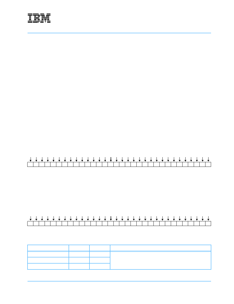
IBM PowerNP NP4GS3
Preliminary
Network Processor
np3_ds_sec10_eppc.fm.11
January 29, 2003
Embedded PowerPCTM Subsystem
Page 423 of 605
10.8.16 PowerPC Subsystem to EPC Doorbell (P2E_Doorbell) Register
The PowerPC subsystem accesses the PowerPC Subsystem to EPC Doorbell register from the PLB, while
the EPC accesses this register from the CAB Interface. The PowerPC subsystem uses this register to signal
interrupts to the EPC. The PowerPC subsystem has read and SUM write access to this register. The data
contains the mask used to access this register. When any of this register's bits are set to `1', an interrupt
signal of the EPC is activated. This register is read by the EPC to determine which doorbells have been acti-
vated. The EPC has read and RUM write access to this register using a CAB address value.
CAB View
PLB View
CAB View
Access Type
CAB
Read/Reset Under Mask Write
PLB
Read/Set Under Mask Write
Base Address
CAB
x`3801 0100'
PLB
x`7801 0070'
P2E_Doorbells
P2E_Msg_D
oorbell 31
P2E_Msg_D
oorbell 30
P2E_Msg_D
oorbell 29
P2E_Msg_D
oorbell 28
P2E_Msg_D
oorbell 27
P2E_Msg_D
oorbell 26
P2E_Msg_D
oorbell 25
P2E_Msg_D
oorbell 24
P2E_Msg_D
oorbell 23
P2E_Msg_D
oorbell 22
P2E_Msg_D
oorbell 21
P2E_Msg_D
oorbell 20
P2E_Msg_D
oorbell 19
P2E_Msg_D
oorbell 18
P2E_Msg_D
oorbell 17
P2E_Msg_D
oorbell 16
P2E_Msg_D
oorbell 15
P2E_Msg_D
oorbell 14
P2E_Msg_D
oorbell 13
P2E_Msg_D
oorbell 12
P2E_Msg_D
oorbell 11
P2E_Msg_D
oorbell 10
P2E_Msg_D
oorbell 9
P2E_Msg_D
oorbell 8
P2E_Msg_D
oorbell 7
P2E_Msg_D
oorbell 6
P2E_Msg_D
oorbell 5
P2E_Msg_D
oorbell 4
P2E_Msg_D
oorbell 3
P2E_Msg_D
oorbell 2
P2E_Msg_D
oorbell 1
P2E_Msg_D
oorbell 0
31 30 29 28 27 26 25 24 23 22 21 20 19 18 17 16 15 14 13 12 11 10
9
8
7
6
5
4
3
2
1
0
P2E_Doorbells
P2E_Msg_
Doorbell 31
P2E_Msg_
Doorbell 30
P2E_Msg_
Doorbell 29
P2E_Msg_
Doorbell 28
P2E_Msg_
Doorbell 27
P2E_Msg_
Doorbell 26
P2E_Msg_
Doorbell 25
P2E_Msg_
Doorbell 24
P2E_Msg_
Doorbell 23
P2E_Msg_
Doorbell 22
P2E_Msg_
Doorbell 21
P2E_Msg_
Doorbell 20
P2E_Msg_
Doorbell 19
P2E_Msg_
Doorbell 18
P2E_Msg_
Doorbell 17
P2E_Msg_
Doorbell 16
P2E_Msg_
Doorbell 15
P2E_Msg_
Doorbell 14
P2E_Msg_
Doorbell 13
P2E_Msg_
Doorbell 12
P2E_Msg_
Doorbell 11
P2E_Msg_
Doorbell 10
P2E_Msg_
Doorbell 9
P2E_Msg_
Doorbell 8
P2E_Msg_
Doorbell 7
P2E_Msg_
Doorbell 6
P2E_Msg_
Doorbell 5
P2E_Msg_
Doorbell 4
P2E_Msg_
Doorbell 3
P2E_Msg_
Doorbell 2
P2E_Msg_
Doorbell 1
P2E_Msg_
Doorbell 0
0
1
2
3
4
5
6
7
8
9
10 11 12 13 14 15 16 17 18 19 20 21 22 23 24 25 26 27 28 29 30 31
Field Name
Bit(s)
Reset
Description
P2E_Msg_Doorbell 31
31
0
PowerPC Subsystem to EPC Doorbell. Indicates which of the 32 possible
doorbells is activated.
0
Not activated
1
Activated
P2E_Msg_Doorbell 30:1
30:1
0 for all
P2E_Msg_Doorbell 0
0
0

IBM PowerNP NP4GS3
Network Processor
Preliminary
Embedded PowerPCTM Subsystem
Page 424 of 605
np3_ds_sec10_eppc.fm.11
January 29, 2003
PLB View
10.8.17 Mailbox Communications Between PCI Host and EPC
Communication between the PCI Host processor and the EPC is accomplished by writing message data into
buffers in the PowerPC DRAM and signalling the destination processor with an interrupt. The PCI Host
processor software manages message data buffers for PCI Host processor to EPC (H2E) messages and
EPC to PCI Host processor (E2H) messages.
Message data buffers are allocated to the EPC by writing the buffers' starting address into the
E2H_Msg_Resource register. Writing this register sets the E2H_Bufr_Valid flag in the Msg_Status register.
This flag indicates to the EPC that the buffer is valid and can be used by the EPC. The EPC reads the
E2H_Bufr_Valid value when a message buffer is required. The EPC then reads the E2H_Msg_Resource
register via the CAB Interface and the E2P_Bufr_Valid indicator bit is reset. By polling this indicator bit, the
PCI Host processor knows when to replenish the E2H_Msg_Resource register with a new buffer address
value. Having acquired a message data buffer, the EPC will compose a message in the buffer and write the
buffer's starting address value into the E2H_Msg_Addr register. Writing to this register generates an interrupt
to the PCI Host processor. The PCI Host processor reads this register to find and process the message.
Reading this register clears the interrupt condition.
Since the PCI Host processor software manages the message data buffers, there is no need for an
H2E_Msg_Resource register. The PCI Host processor composes a message in one of the data buffers and
writes the starting address of the buffer into the H2E_Msg_Addr register. Writing to this register produces an
interrupt input signal to the EPC and sets the H2E_Msg_Busy bit of the Msg_Status register. As long as this
flag is set, the EPC is processing the message buffer. The EPC reads the H2E_Msg_Addr register to locate
the buffer in the PowerPC DRAM and reset the interrupt input signal to the EPC. The EPC resets the
H2E_Msg_Busy bit by reading the P2E_Msg_Addr register from an alternate CAB address when message
processing is complete. The PCI Host processor will poll the H2E_Msg_Busy bit to determine when the buffer
can be reused.
Field Name
Bit(s)
Reset
Description
P2E_Msg_Doorbell 31
0
0
PowerPC Subsystem to EPC Doorbell. Indicates which of the 32 possible
doorbells is activated.
0
Not activated
1
Activated
P2E_Msg_Doorbell 30:1
1:30
0 for all
P2E_Msg_Doorbell 0
31
0

IBM PowerNP NP4GS3
Preliminary
Network Processor
np3_ds_sec10_eppc.fm.11
January 29, 2003
Embedded PowerPCTM Subsystem
Page 425 of 605
10.8.18 EPC to PCI Host Resource (E2H_Msg_Resource) Register
The PCI Host processor accesses the EPC to PCI Host Message Resource register from the PLB while the
EPC accesses this register from its CAB Interface. This EPC uses this register to obtain message buffers in
the PowerPC DRAM address space for messages it sends to the PCI Host processor. The PCI Host
processor writes the starting DRAM address value of a message buffer into the E2P_Msg_Resource register.
Writing to this register sets the E2H_Bufr_Valid flag found in the Message Status register (see 10.8.23
Message Status (Msg_Status) Register on page 431). Reading the E2H_Msg_Resource register from the
CAB resets this flag.
CAB View
PLB View
CAB View
PLB View
Access Type
CAB
Read
(Additional actions occur when reading this register using
this address. See register description for details.)
PLB
Read/Write
Base Address
CAB
x`3801 0200'
PLB
x`7801 0080'
E2H_Msg_Resource
31 30 29 28 27 26 25 24 23 22 21 20 19 18 17 16 15 14 13 12 11 10
9
8
7
6
5
4
3
2
1
0
E2H_Msg_Resource
0
1
2
3
4
5
6
7
8
9
10 11 12 13 14 15 16 17 18 19 20 21 22 23 24 25 26 27 28 29 30 31
Field Name
Bit(s)
Reset
Description
E2H_Msg_Resource
31:0
x'0000 0000'
EPC to PCI Host Message Resource - written with the PowerPC DRAM
starting address of a message buffer. When reading this register via the
CAB, the E2H_Bufr_Valid flag found in the Message Status Register (see
10.8.23 Message Status (Msg_Status) Register on page 431) is set to 0.
Field Name
Bit(s)
Reset
Description
E2H_Msg_Resource
0:31
x'0000 0000'
EPC to PCI Host Message Resource - written with the PowerPC DRAM
starting address of a message buffer. When writing this register, the
E2H_Bufr_Valid flag is set to 1.

IBM PowerNP NP4GS3
Network Processor
Preliminary
Embedded PowerPCTM Subsystem
Page 426 of 605
np3_ds_sec10_eppc.fm.11
January 29, 2003
10.8.19 EPC to PCI Host Message Address (E2H_Msg_Addr) Register
The PCI Host Processor accesses the EPC to PCI Host Message Address register from the PLB while the
EPC accesses this register from its CAB Interface. The EPC uses this register to send messages to the PCI
Host processor. The value written into this register is the PowerPC DRAM address at which the message
begins. Writing to this register sets the E2H_msg bit of the PCI_Interr_Status register. When the corre-
sponding bit of the PCI_Interr_Ena register is set to `1', an interrupt signal to the PCI Host processor is acti-
vated. Reading the E2H_Msg_Addr register from the PLB resets the E2H_msg bit of the PCI_Interr_Status
register.
CAB View
PLB View
CAB View
PLB View
Access Type
CAB
Read/Write
PLB
Read
Base Address
CAB
x`3801 0400'
PLB
x`7801 0088'
(Additional actions occur when reading this register using
this address. See register description for details.)
E2H_Msg_Addr
31 30 29 28 27 26 25 24 23 22 21 20 19 18 17 16 15 14 13 12 11 10
9
8
7
6
5
4
3
2
1
0
E2H_Msg_Addr
0
1
2
3
4
5
6
7
8
9
10 11 12 13 14 15 16 17 18 19 20 21 22 23 24 25 26 27 28 29 30 31
Field Name
Bit(s)
Reset
Description
E2H_Msg_Addr
31:0
x'0000 0000'
EPC to PCI Host Message Address - indicates the PowerPC DRAM start-
ing address of a message.
Field Name
Bit(s)
Reset
Description
E2H_Msg_Addr
0:31
x'0000 0000'
EPC to PCI Host Message Address - indicates the PowerPC DRAM start-
ing address of a message.

IBM PowerNP NP4GS3
Preliminary
Network Processor
np3_ds_sec10_eppc.fm.11
January 29, 2003
Embedded PowerPCTM Subsystem
Page 427 of 605
10.8.20 EPC to PCI Host Doorbell (E2H_Doorbell) Register
The PCI Host Processor accesses the EPC to PCI Host Doorbell register from the PLB while the EPC
accesses this register from the CAB Interface. The EPC uses this register to signal interrupts to the PCI Host
processor. The EPC has read and SUM write access to this register using a CAB address value. The mask
used to access this register is contained in the data. When any of this register's bits are set to `1' and the
corresponding bit of the PCI_Interr_Ena register is set to `1', an interrupt signal of the PCI Host processor is
activated. This register is read by the PCI Host processor to determine which of the doorbells have been acti-
vated. The PCI Host processor has read and RUM write and read access to this register using a PLB address
value.
CAB View
PLB View
CAB View
Access Type
CAB
Read/Set Under Mask Write
PLB
Read/Reset Under Mask Write
Base Address
CAB
x`3801 0800'
PLB
x`7801 0098'
E2H_Doorbells
E2H_Msg_Doo
rbell 31
E2H_Msg_Doo
rbell 30
E2H_Msg_Doo
rbell 29
E2H_Msg_Doo
rbell 28
E2H_Msg_Doo
rbell 27
E2H_Msg_Doo
rbell 26
E2H_Msg_Doo
rbell 25
E2H_Msg_Doo
rbell 24
E2H_Msg_Doo
rbell 23
E2H_Msg_Doo
rbell 22
E2H_Msg_Doo
rbell 21
E2H_Msg_Doo
rbell 20
E2H_Msg_Doo
rbell 19
E2H_Msg_Doo
rbell 18
E2H_Msg_Doo
rbell 17
E2H_Msg_Doo
rbell 16
E2H_Msg_Doo
rbell 15
E2H_Msg_Doo
rbell 14
E2H_Msg_Doo
rbell 13
E2H_Msg_Doo
rbell 12
E2H_Msg_Doo
rbell 11
E2H_Msg_Doo
rbell 10
E2H_Msg_Doo
rbell 9
E2H_Msg_Doo
rbell 8
E2H_Msg_Doo
rbell 7
E2H_Msg_Doo
rbell 6
E2H_Msg_Doo
rbell 5
E2H_Msg_Doo
rbell 4
E2H_Msg_Doo
rbell 3
E2H_Msg_Doo
rbell 2
E2H_Msg_Doo
rbell 1
E2H_Msg_Doo
rbell 0
31 30 29 28 27 26 25 24 23 22 21 20 19 18 17 16 15 14 13 12 11 10
9
8
7
6
5
4
3
2
1
0
E2H_Doorbells
E2H
_
Msg_D
oorbell 31
E2H
_
Msg_D
oorbell 30
E2H
_
Msg_D
oorbell 29
E2H
_
Msg_D
oorbell 28
E2H
_
Msg_D
oorbell 27
E2H
_
Msg_D
oorbell 26
E2H
_
Msg_D
oorbell 25
E2H
_
Msg_D
oorbell 24
E2H
_
Msg_D
oorbell 23
E2H
_
Msg_D
oorbell 22
E2H
_
Msg_D
oorbell 21
E2H
_
Msg_D
oorbell 20
E2H
_
Msg_D
oorbell 19
E2H
_
Msg_D
oorbell 18
E2H
_
Msg_D
oorbell 17
E2H
_
Msg_D
oorbell 16
E2H
_
Msg_D
oorbell 15
E2H
_
Msg_D
oorbell 14
E2H
_
Msg_D
oorbell 13
E2H
_
Msg_D
oorbell 12
E2H
_
Msg_D
oorbell 11
E2H
_
Msg_D
oorbell 10
E2H
_
Msg_D
oorbell 9
E2H
_
Msg_D
oorbell 8
E2H
_
Msg_D
oorbell 7
E2H
_
Msg_D
oorbell 6
E2H
_
Msg_D
oorbell 5
E2H
_
Msg_D
oorbell 4
E2H
_
Msg_D
oorbell 3
E2H
_
Msg_D
oorbell 2
E2H
_
Msg_D
oorbell 1
E2H
_
Msg_D
oorbell 0
0
1
2
3
4
5
6
7
8
9
10 11 12 13 14 15 16 17 18 19 20 21 22 23 24 25 26 27 28 29 30 31
Field Name
Bit(s)
Reset
Description
E2H_Msg_Doorbell 31
31
0
EPC to PCI Host Doorbell - indicates which of the 32 possible doorbells is
activated.
0
Not activated
1
Activated
E2H_Msg_Doorbell 30:1
30:1
0 for all
E2H_Msg_Doorbell 0
0
0

IBM PowerNP NP4GS3
Network Processor
Preliminary
Embedded PowerPCTM Subsystem
Page 428 of 605
np3_ds_sec10_eppc.fm.11
January 29, 2003
PLB View
Field Name
Bit(s)
Reset
Description
E2H_Msg_Doorbell 31
0
0
EPC to PCI Host Doorbell - indicates which of the 32 possible doorbells is
activated.
0
Not activated
1
Activated
E2H_Msg_Doorbell 30:1
1:30
0 for all
E2H_Msg_Doorbell 0
31
0

IBM PowerNP NP4GS3
Preliminary
Network Processor
np3_ds_sec10_eppc.fm.11
January 29, 2003
Embedded PowerPCTM Subsystem
Page 429 of 605
10.8.21 PCI Host to EPC Message Address (H2E_Msg_Addr) Register
The PCI Host processor accesses the PCI Host to EPC Message Address register from the PLB while the
EPC accesses this register from the CAB Interface. The PCI Host uses this register to send messages to the
EPC. The value written into this register is the PowerPC DRAM address at which the message begins.
Writing to this register sets the H2E_Msg_Interr signal to the EPC and the H2E_Msg_Busy bit of the
Msg_Status register. Reading the H2E_Msg_Addr register from the primary CAB address will reset the
H2E_Msg_Interr signal to the EPC. Reading the H2E_Msg_Addr from the alternate CAB address will reset
the H2E_Msg_Busy bit of the Msg_Status register (see 10.8.23 Message Status (Msg_Status) Register on
page 431).
CAB View
PLB View
CAB View
PLB View
Access Type
Primary
Read
Alternate
Read
PLB
Read/Write
Base Address
Primary
x`3801 1000'
(Additional actions occur when reading this register using
this address. See register description for details.)
Alternate
x`3802 0020'
(Additional actions occur when reading this register using
this address. See register description for details.)
PLB
x`7801 00A8'
H2E_Msg_Addr
31 30 29 28 27 26 25 24 23 22 21 20 19 18 17 16 15 14 13 12 11 10
9
8
7
6
5
4
3
2
1
0
H2E_Msg_Addr
0
1
2
3
4
5
6
7
8
9
10 11 12 13 14 15 16 17 18 19 20 21 22 23 24 25 26 27 28 29 30 31
Field Name
Bit(s)
Reset
Description
H2E_Msg_Addr
31:0
x'0000 0000'
PCI Host to EPC Message Address - indicates a message's PowerPC
DRAM starting address.
Field Name
Bit(s)
Reset
Description
H2E_Msg_Addr
0:31
x'0000 0000'
PCI Host to EPC Message Address - indicates a message's PowerPC
DRAM starting address.

IBM PowerNP NP4GS3
Network Processor
Preliminary
Embedded PowerPCTM Subsystem
Page 430 of 605
np3_ds_sec10_eppc.fm.11
January 29, 2003
10.8.22 PCI Host to EPC Doorbell (H2E_Doorbell) Register
The PCI Host processor accesses the PCI Host to EPC Doorbell register from the PLB while the EPC
accesses this register from the CAB Interface. The PCI Host processor uses this register to signal interrupts
to the EPC. The PCI Host processor has read and SUM write access to this register. The data contains the
mask used to access this register. When any of this register's bits are set to `1', an interrupt signal of the EPC
is activated. This register is read by the EPC to determine which of the doorbells have been activated. The
EPC has read and RUM write access to this register using a CAB address value.
CAB View
PLB View
CAB View
Access Type
CAB
Read/Reset Under Mask Write
PLB
Read/Set Under Mask Write
Base Address
CAB
x`3801 2000'
PLB
x`7801 00B0'
H2E_Doorbells
H2E_Msg_Doo
rbell 31
H2E_Msg_Doo
rbell 30
H2E_Msg_Doo
rbell 29
H2E_Msg_Doo
rbell 28
H2E_Msg_Doo
rbell 27
H2E_Msg_Doo
rbell 26
H2E_Msg_Doo
rbell 25
H2E_Msg_Doo
rbell 24
H2E_Msg_Doo
rbell 23
H2E_Msg_Doo
rbell 22
H2E_Msg_Doo
rbell 21
H2E_Msg_Doo
rbell 20
H2E_Msg_Doo
rbell 19
H2E_Msg_Doo
rbell 18
H2E_Msg_Doo
rbell 17
H2E_Msg_Doo
rbell 16
H2E_Msg_Doo
rbell 15
H2E_Msg_Doo
rbell 14
H2E_Msg_Doo
rbell 13
H2E_Msg_Doo
rbell 12
H2E_Msg_Doo
rbell 11
H2E_Msg_Doo
rbell 10
H2E_Msg_Doo
rbell 9
H2E_Msg_Doo
rbell 8
H2E_Msg_Doo
rbell 7
H2E_Msg_Doo
rbell 6
H2E_Msg_Doo
rbell 5
H2E_Msg_Doo
rbell 4
H2E_Msg_Doo
rbell 3
H2E_Msg_Doo
rbell 2
H2E_Msg_Doo
rbell 1
H2E_Msg_Doo
rbell 0
31 30 29 28 27 26 25 24 23 22 21 20 19 18 17 16 15 14 13 12 11 10
9
8
7
6
5
4
3
2
1
0
H2E_Doorbells
H
2
E_Msg_
Doorbell 31
H
2
E_Msg_
Doorbell 30
H
2
E_Msg_
Doorbell 29
H
2
E_Msg_
Doorbell 28
H
2
E_Msg_
Doorbell 27
H
2
E_Msg_
Doorbell 26
H
2
E_Msg_
Doorbell 25
H
2
E_Msg_
Doorbell 24
H
2
E_Msg_
Doorbell 23
H
2
E_Msg_
Doorbell 22
H
2
E_Msg_
Doorbell 21
H
2
E_Msg_
Doorbell 20
H
2
E_Msg_
Doorbell 19
H
2
E_Msg_
Doorbell 18
H
2
E_Msg_
Doorbell 17
H
2
E_Msg_
Doorbell 16
H
2
E_Msg_
Doorbell 15
H
2
E_Msg_
Doorbell 14
H
2
E_Msg_
Doorbell 13
H
2
E_Msg_
Doorbell 12
H
2
E_Msg_
Doorbell 11
H
2
E_Msg_
Doorbell 10
H
2
E_Msg_
Doorbell 9
H
2
E_Msg_
Doorbell 8
H
2
E_Msg_
Doorbell 7
H
2
E_Msg_
Doorbell 6
H
2
E_Msg_
Doorbell 5
H
2
E_Msg_
Doorbell 4
H
2
E_Msg_
Doorbell 3
H
2
E_Msg_
Doorbell 2
H
2
E_Msg_
Doorbell 1
H
2
E_Msg_
Doorbell 0
0
1
2
3
4
5
6
7
8
9
10 11 12 13 14 15 16 17 18 19 20 21 22 23 24 25 26 27 28 29 30 31
Field Name
Bit
Reset
Description
H2E_Msg_Doorbell 31
31
0
PCI Host to EPC Doorbell - indicates which of the 32 possible doorbells
have been activated.
0
Not activated
1
Activated
H2E_Msg_Doorbell 30:1
30:1
0 for all
H2E_Msg_Doorbell 0
0
0

IBM PowerNP NP4GS3
Preliminary
Network Processor
np3_ds_sec10_eppc.fm.11
January 29, 2003
Embedded PowerPCTM Subsystem
Page 431 of 605
PLB View
10.8.23 Message Status (Msg_Status) Register
The Message Status register provides status information associated with inter-processor messaging. This
read only register is accessible from either the PLB or the CAB for the purpose of checking status associated
with messaging.
CAB View
PLB View
Field Name
PLB Bit
Reset
Description
H2E_Msg_Doorbell 31
0
0
PCI Host to EPC Doorbell - indicates which of the 32 possible doorbells is
activated.
0
Not activated
1
Activated
H2E_Msg_Doorbell 30:1
1:30
0 for all
H2E_Msg_Doorbell 0
31
0
Access Type
CAB
Read
PLB
Read
Base Address
CAB
x`3801 4000'
PLB
x`7801 00A0'
Reserved
P2H_Bufr_Val
id
H2P_Msg_Busy
E2P_Bufr_Valid
P2E_Msg_Busy
E2H_Bufr_Val
id
H2E_Msg_Busy
31 30 29 28 27 26 25 24 23 22 21 20 19 18 17 16 15 14 13 12 11 10
9
8
7
6
5
4
3
2
1
0
Reserved
P2H_Bufr_
V
a
l
id
H2P_Msg_Busy
E2P_Bufr_Vali
d
P2E_Ms
g_
B
u
s
y
E2H_Bufr_
V
a
l
id
H2E_Msg_Busy
0
1
2
3
4
5
6
7
8
9
10 11 12 13 14 15 16 17 18 19 20 21 22 23 24 25 26 27 28 29 30 31

IBM PowerNP NP4GS3
Network Processor
Preliminary
Embedded PowerPCTM Subsystem
Page 432 of 605
np3_ds_sec10_eppc.fm.11
January 29, 2003
CAB View
PLB View
Field Name
CAB Bit(s)
Reset
Description
Reserved
31:6
Reserved
P2H_Bufr_Valid
5
0
PowerPC subsystem to PCI Host message buffer valid indicator.
0
Buffer not valid
1
Buffer valid
H2P_Msg_Busy
4
0
PCI Host to PowerPC subsystem message busy indicator.
0
Not busy processing H2P message
1
Busy processing H2P message
E2P_Bufr_Valid
3
0
EPC to PowerPC subsystem message buffer valid indicator.
0
Buffer not valid
1
Buffer valid
P2E_Msg_Busy
2
0
PowerPC to EPC subsystem message busy indicator.
0
Not busy processing P2E message
1
Busy processing P2E message
E2H_Bufr_Valid
1
0
EPC to PCI Host message buffer valid indicator.
0
Buffer not valid
1
Buffer valid
H2E_Msg_Busy
0
0
PCI Host to EPC message busy indicator.
0
Not busy processing H2E message
1
Busy processing H2E message
Field Name
Bit(s)
Reset
Description
Reserved
0:25
Reserved
P2H_Bufr_Valid
26
0
PowerPC subsystem to PCI Host message buffer valid indicator.
0
Buffer not valid
1
Buffer valid
H2P_Msg_Busy
27
0
PCI Host to PowerPC subsystem message busy indicator.
0
Not busy processing H2P message
1
Busy processing H2P message
E2P_Bufr_Valid
28
0
EPC to PowerPC subsystem message buffer valid indicator.
0
Buffer not valid
1
Buffer valid
P2E_Msg_Busy
29
0
PowerPC subsystem to EPC message busy indicator.
0
Not busy processing P2E message
1
Busy processing P2E message
E2H_Bufr_Valid
30
0
EPC to PCI Host message buffer valid indicator.
0
Buffer not valid
1
Buffer valid
H2E_Msg_Busy
31
0
PCI Host to EPC message busy indicator.
0
Not busy processing H2E message
1
Busy processing H2E message

IBM PowerNP NP4GS3
Preliminary
Network Processor
np3_ds_sec10_eppc.fm.11
January 29, 2003
Embedded PowerPCTM Subsystem
Page 433 of 605
10.8.24 PowerPC Boot Redirection Instruction Registers (Boot_Redir_Inst)
In system implementations in which the embedded PowerPC subsystem boots from the D6 DRAM, the
Mailbox and DRAM Interface macro performs PowerPC boot address redirection. Under these conditions, the
hardware provides instructions that redirect the boot sequence to a location in the PowerPC DRAM. Storage
for eight instructions is provided by the Boot_Redir_Inst registers.
The PowerPC Boot Redirection Instruction (Boot_Redir_Inst) registers are accessed from the CAB Interface.
These registers provide capacity for eight instructions for PLB addresses x`FFFF FFE0' - x`FFFF FFFC'
These instructions redirect the PowerPC subsystem to boot from a location in the PowerPC DRAM and are
configured before the PPC_Reset is cleared.
Access Type
Read/Write
Base Address
x`3800 0110' - x`3800 0117'
Boot_Redir_Inst
31 30 29 28 27 26 25 24 23 22 21 20 19 18 17 16 15 14 13 12 11 10
9
8
7
6
5
4
3
2
1
0
Field Name
Bit(s)
Reset
Description
Boot_Redir_Inst 31:0
x`0000
0000'
PowerPC boot redirection instruction address values contains instructions
used by the PowerPC subsystem to redirect the boot sequence to a loca-
tion in D6 DRAM.
Offset
Corresponding PowerPC Instruction Address
0
x`FFFF FFE0'
1
x`FFFF FFE4'
2
x`FFFF FFE8'
3
x`FFFF FFEC'
4
x`FFFF FFF0'
5
x`FFFF FFF4'
6
x`FFFF FFF8'
7
x`FFFF FFFC'

IBM PowerNP NP4GS3
Network Processor
Preliminary
Embedded PowerPCTM Subsystem
Page 434 of 605
np3_ds_sec10_eppc.fm.11
January 29, 2003
10.8.25 PowerPC Machine Check (PwrPC_Mach_Chk) Register
This register is accessible on the CAB and indicates the status of the machine check output of the PowerPC
processor core.
10.8.26 Parity Error Status and Reporting
When reading the PowerPC subsystem memory, any parity errors encountered are recorded and actions are
taken. PowerPC subsystem memory parity errors are indicated for each double word returned on the PLB
regardless of the object size read. For this reason, parity must be initialized for every double word in each
memory region used. Furthermore, for PowerPC processor code regions, correct parity must be initialized for
each cache line in the region. Parity will be set correctly when the memory is written. Therefore, for code
regions, this parity initialization is accomplished automatically when the code is loaded. Likewise, this initial-
ization is performed if a diagnostic is performed on the memory that writes to every location. In all other
cases, this parity initialization must be performed for each region of memory used prior to use.
Since even bytes and odd bytes of the PowerPC subsystem memory are stored in physically distinct mod-
ules, error statistics are collected on an odd and even byte basis. This information may prove useful in isola-
tion of a failing part. The word address value of the most recent parity error is stored in the Slave Error
Address Register (SEAR). In addition, bits of the Slave Error Status Register (SESR) indicate which PLB
masters have experienced parity errors in reading the PowerPC subsystem memory. This status information
is indicated by odd and even byte for each of the three PLB masters (Instruction Cache Unit, Data Cache
Unit, and PCI/PLB macro).
Bits of the SESR are used to generate an interrupt input to the UIC. If any of these bits are set to b'1' then the
parity error interrupt input to the UIC is set to b'1'. When the UIC is configured to enable this interrupt input,
an interrupt signal is generated to the PPC405 Core for processing. As a part of the interrupt service routine,
the SESR must be read to clear the source of the interrupt.
Access Type
Read
Base Address (CAB)
x`3800 0210'
Reserved
Ma
ch_C
hk
31 30 29 28 27 26 25 24 23 22 21 20 19 18 17 16 15 14 13 12 11 10
9
8
7
6
5
4
3
2
1
0
Field Name
Bit(s)
Reset
Description
Reserved
31:1
Reserved
Mach_Chk 0
0
PowerPC machine check indication.
0
No machine check has occurred
1
A machine check has occurred

IBM PowerNP NP4GS3
Preliminary
Network Processor
np3_ds_sec10_eppc.fm.11
January 29, 2003
Embedded PowerPCTM Subsystem
Page 435 of 605
10.8.27 Slave Error Address Register (SEAR)
The Slave Error Address Register records the word address value of the last occurrence of a parity error
encountered by the DRAM Interface slave unit. This address value will isolate the location of the parity error
to within a word.
Access Type
Read
Base Address (PLB)
x`7801 00B8'
Error Address
0
1
2
3
4
5
6
7
8
9
10 11 12 13 14 15 16 17 18 19 20 21 22 23 24 25 26 27 28 29 30 31
Field Name
Bit(s)
Reset
Description
Error Address
0:31
x'0000 0000'
Last PLB word address value that resulted in a parity error when using the
DRAM Interface slave unit.

IBM PowerNP NP4GS3
Network Processor
Preliminary
Embedded PowerPCTM Subsystem
Page 436 of 605
np3_ds_sec10_eppc.fm.11
January 29, 2003
10.8.28 Slave Error Status Register (SESR)
The Slave Error Status Register contains status information that indicates which masters have encountered
parity errors in reading from the DRAM and whether these errors occurred in a byte with an even
(Perr_Byte0) or an odd (Perr_Byte1) address value. The PowerPC subsystem has three PLB masters: the
Instruction Cache Unit (ICU), the Data Cache Unit (DCU), and the PCI macro. The contents of this register
are reset to x`0000 0000' when read.
Access Type
Read and Reset
Base Address (PLB)
x`7801 00C0'
ICU_Error_Status
DCU_Error_Status
PCI_Error_Status
Reserved
perr_byte0
perr_byte1
Reserved
perr_byte0
perr_byte1
Reserved
perr_byte0
perr_byte1
Reserved
0
1
2
3
4
5
6
7
8
9
10 11 12 13 14 15 16 17 18 19 20 21 22 23 24 25 26 27 28 29 30 31
Field Name
Bit(s)
Reset
Description
Reserved
0:5
Reserved
Perr_Byte0
6
0
Byte 0 parity error indication - whether or not the Instruction Cache Unit
PLB master encountered a parity error since the register was last read.
0
No parity error encountered
1
Parity error encountered
Perr_Byte1
7
0
Byte 1 parity error indication - whether or not the Instruction Cache Unit
PLB master encountered a parity error since the register was last read.
0
No parity error encountered
1
Parity error encountered
Reserved
8:13
Reserved
Perr_Byte0
14
0
Byte 0 parity error indication - whether or not the Data Cache Unit PLB
master encountered a parity error since the register was last read.
0
No parity error encountered
1
Parity error encountered
Perr_Byte1
15
0
Byte 1 parity error indication - whether or not the Data Cache Unit PLB
master encountered a parity error since the register was last read.
0
No parity error encountered
1
Parity error encountered
Reserved
16:21
Reserved
Perr_Byte0
22
0
Byte 0 parity error indication - whether or not the PCI Macro PLB master
encountered a parity error since the register was last read.
0
No parity error encountered
1
Parity error encountered
Perr_Byte1
23
0
Byte 1 parity error indication - whether or not the PCI Macro PLB master
encountered a parity error since the register was last read.
0
No parity error encountered
1
Parity error encountered
Reserved
24:31
Reserved
IBM PowerNP NP4GS3
Preliminary
Network Processor
np3_ds_sec10_eppc.fm.11
January 29, 2003
Embedded PowerPCTM Subsystem
Page 437 of 605
10.8.29 Parity Error Counter (Perr_Count) Register
The Parity Error Counter register contains two 16-bit counter values. These counters accumulate the total
number of parity errors for even and odd byte addresses since the last time the chip was reset. These
counters roll over to zero when their maximum value is reached (65535).
Access Type
Read
Base Address (PLB)
x`7801 00C8'
Byte0_Perr_Count
Byte1_Perr_Count
0
1
2
3
4
5
6
7
8
9
10 11 12 13 14 15 16 17 18 19 20 21 22 23 24 25 26 27 28 29 30 31
Field Name
Bit(s)
Reset
Description
Byte0_Perr_Count
0:15
x'0000'
Count of byte 0 parity errors encountered when reading DRAM from
DRAM Interface slave unit.
Byte1_Perr_Count
16:31
x'0000'
Count of byte 1parity errors encountered when reading DRAM from
DRAM Interface slave unit.

IBM PowerNP NP4GS3
Network Processor
Preliminary
Embedded PowerPCTM Subsystem
Page 438 of 605
np3_ds_sec10_eppc.fm.11
January 29, 2003
10.9 System Start-Up and Initialization
10.9.1 NP4GS3 Resets
A general reset is performed whenever the NP4GS3's Reset input pin is activated. A general reset includes
the PowerPC Core, and the NP4GS3 Network Function reset domains. The PowerPC Core and the NP4GS3
Network Function reset domains are also controlled by separate configuration registers, PowerPC_Reset and
Soft_Reset, respectively. Each of these registers are accessible via the NP4GS3's CAB Interface. A general
reset sets the PowerPC_Reset to `1' (activated), but the Soft_Reset will be set to `0' (deactivated).
When the general reset is deactivated, the PowerPC Core remains in reset and the PowerPC Macros and the
NP4GS3 Network Function are in an idle condition with state machines active and control structures un-
initialized. The NP4GS3 Network Function will be functional once EPC picocode has been loaded and control
structures are initialized. The EPC is activated automatically when loading boot picocode from the SPM inter-
face or by setting the BD_Override bit to `1' in the Boot Override register (see 13.14.4 Boot Override Register
(Boot_Override) on page 495). The PowerPC Core is activated by clearing the bit of the PowerPC_Reset
register.
The PowerPC Core and the NP4GS3 Network Function domains are separately reset and activated by
setting and clearing their respective reset registers. Setting the control bit in the Soft_Reset register causes
the Network Function to be momentarily reset while the PowerPC subsystem
is held in reset. The
PowerPC_Reset is also activated whenever the Watch Dog timer of the PowerPC Core expires for a second
time and Watch Dog Reset Enable (WD_Reset_Ena) is set to `1'. When enabled, the second expiration of the
Watch Dog timer results in a pulse on the SERR# signal of the PCI Bus. The TCR [WRC] of the PowerPC
Core is set to `10' to generate a chip reset request on the second expiration of the Watch Dog timer.
The PowerPC Core can be reset from the RISCWatch debugger environment. A Core reset performed from
RISCWatch resets the PPC405 Core, but does not set the PowerPC_Reset control register. This allows a
momentary reset of the PowerPC Core and does not require a release of the PowerPC Core by clearing the
PowerPC_Reset control register. The PowerPC Core is also reset and the PowerPC_Reset control register is
set when a `chip reset' command is performed from RISCWatch and the Watch Dog Reset Enable is set to
`1'. This resets the PowerPC Core and holds it in reset until the PowerPC_Reset register is cleared.
Table 10-10. Reset Domains
Reset Domain
Applies
PowerPC Core
Applies only to the PPC405 processor core and is used to control its start-up during system initialization
Network Function
Applies to all other functions in the NP4GS3

IBM PowerNP NP4GS3
Preliminary
Network Processor
np3_ds_sec10_eppc.fm.11
January 29, 2003
Embedded PowerPCTM Subsystem
Page 439 of 605
10.9.2 Systems Initialized by External PCI Host Processors
System implementations with control function centralized in a PCI Host processor are initialized primarily by
an external PCI Host processor. These systems do not use the SPM Interface or its associated flash memory
to boot the EPC and DASL picocode (Boot_Picocode = '1'). The host processor (Boot_PPC = '0') loads code
for the PowerPC processor and the EPC and DASL picoprocessors.
The general sequence of the start-up and initialization is as follows:
1. The host processor boots and performs blade level configuration and testing while holding blade sub-
systems in reset.
2. The host processor releases each of the blade subsystems' reset signals in sequence.
3. Release of the general reset input pin of the NP4GS3 activates its state machines. The NP4GS3 is in an
idle state with un-initialized structures and the PPC405 Core remains in reset and Host PCI Configuration
is enabled.
4. The host system uses the PCI Configuration protocol to configure internal registers of the PCI Interface
Macro. This configuration sets the base address values of the PCI Target Maps. The PCI Master Maps
are disabled.
5. The host processor uses the appropriate PCI target address values to configure and initialize the
NP4GS3's DRAM controllers via the CAB Interface.
6. The host processor uses the appropriate PCI target address values to load the PowerPC code into one of
the NP4GS3's DRAMs. This code includes the branch code loaded into the Boot_Redir_Inst registers.
7. The host loads the picocode memories of the EPC and DASL. These memories are accessible via the
CAB Interface macro. The addresses of the registers controlling this interface were mapped to PCI
addresses in step 4.
8. The host processor starts the PPC405 Core by clearing the PowerPC_Reset configuration register. This
register is accessed via the CAB Interface. The PowerPC subsystem starts by fetching the instruction at
PLB address x`FFFF FFFC'. This address is decoded by hardware to provide an unconditional branch to
instruction space in the PowerPC DRAM memory.
9. The host processor uses the CAB Interface to set the BD_Override bit to `1' in the Boot Override register
(see 13.14.4 Boot Override Register (Boot_Override) on page 495) to start the EPC code. This code
controls the initialization of the NP4GS3 structures in preparation for network traffic. Alternatively, this ini-
tialization is performed by the host processor via the CAB Interface.
10. Communication ports are configured and enabled by either the host processor or the PPC405 Core.

IBM PowerNP NP4GS3
Network Processor
Preliminary
Embedded PowerPCTM Subsystem
Page 440 of 605
np3_ds_sec10_eppc.fm.11
January 29, 2003
10.9.3 Systems with PCI Host Processors and Initialized by PowerPC Subsystem
The PowerPC subsystem primarily controls start-up and initialization sequences of systems of this category.
These systems do not use the SPM Interface or its associated flash memory for booting the EPC boot pico-
code (Boot_Picocode = '1'). The PowerPC subsystem boots from PCI address space (Boot_PPC = '1') and
loads code for the PowerPC processor and the EPC and DASL picoprocessors.
The general sequence of the start-up and initialization is as follows:
1. The host processor boots and performs blade level configuration and testing while holding blade sub-
systems in reset.
2. The host processor releases each of the blade subsystems' reset signals in sequence.
3. Release of the general reset input pin of the NP4GS3 activates its state machines. The NP4GS3 is in an
idle state with un-initialized structures and the PPC405 Core remains in reset and Host PCI Configuration
is enabled.
4. The host system uses the PCI Configuration protocol to configure internal registers of the PCI Interface
Macro. This configuration sets the base address values of the PCI Target Maps. The PCI Master Maps
are disabled except for the PMM0 which maps PLB addresses x`FFFE 0000' through x`FFFF FFFF' to the
same addresses in PCI address space.
5. The host processor starts the PPC405 Core by clearing the PowerPC_Reset configuration register. This
register is accessed via the CAB Interface.
6. The PPC405 Core will boot from code residing in the PCI address space starting at address
x`FFFF FFFC'.
7. The PPC405 Core processor configures and initializes the NP4GS3's DRAM controllers via the CAB
Interface.
8. The PPC405 Core processor loads the PowerPC code, via the DRAM Interface Macro, into one of the
NP4GS3's DRAMs.
9. The PPC405 Core processor loads the picocode for the EPC and DASL via the CAB Interface.
10. Using the CAB Interface, the host processor sets the BD_Override bit to `1' in the Boot Override register
(see 13.14.4 Boot Override Register (Boot_Override) on page 495) to start the EPC picocode. This pico-
code will control the initialization of the NP4GS3 structures in preparation for network traffic. Alternatively,
this initialization is performed by the PPC405 Core processor via the CAB Interface.
11. Communication ports are configured and enabled by the PPC405 Core.

IBM PowerNP NP4GS3
Preliminary
Network Processor
np3_ds_sec10_eppc.fm.11
January 29, 2003
Embedded PowerPCTM Subsystem
Page 441 of 605
10.9.4 Systems Without PCI Host Processors and Initialized by PowerPC Subsystem
The EPC initially controls start-up and initialization sequences of systems of this category, but they are prima-
rily controlled by the PowerPC subsystem. These systems use the SPM Interface and its associated flash
memory for booting the EPC picocode (Boot_Picocode = '0'). The PowerPC subsystem boots from PCI
address space ( Boot_PPC = '1') and loads code for the PowerPC processor and the EPC and DASL picopro-
cessors.
The general sequence of the start-up and initialization is as follows:
1. Release of the general reset input pin of the NP4GS3 activates its state machines. The PCI Master Maps
are disabled except for the PMM0 which maps PLB addresses x`FFFE 0000' through x`FFFF FFFF' to the
same addresses in PCI address space. EPC boot picocode is loaded from the flash memory via the SPM
Interface. The SPM Interface automatically starts the EPC and the PPC405 Core remains in reset.
2. EPC code executes diagnostic and initialization code which includes the initialization of the NP4GS3's
DRAM controllers.
3. The EPC starts the PPC405 Core by clearing the PowerPC_Reset configuration register. This register is
accessed via the CAB Interface.
4. The PPC405 Core will boot from code residing in the PCI address space starting at address
x`FFFF FFFC'.
5. The PPC405 Core processor loads the PowerPC code via the DRAM Interface Macro into one of the
NP4GS3's DRAMs.
6. The PPC405 Core processor or the EPC loads the picocode for the DASL via the CAB Interface.
7. Communication ports are configured and enabled by the PPC405 Core.

IBM PowerNP NP4GS3
Network Processor
Preliminary
Embedded PowerPCTM Subsystem
Page 442 of 605
np3_ds_sec10_eppc.fm.11
January 29, 2003
10.9.5 Systems Without PCI Host or Delayed PCI Configuration and Initialized by EPC
The EPC controls start-up and initialization sequences of systems of this category. These systems use the
SPM Interface and its associated flash memory for booting the EPC picocode (Boot_Picocode = '0'). Code for
the PowerPC subsystem and the EPC are loaded by the SPM Interface and the EPC (Boot_PPC = '0'). Code
for the PowerPC subsystem exists in the flash memory or is provided using Guided Traffic.
The general sequence of the start-up and initialization is as follows:
1. Release of the general reset input pin of the NP4GS3 activates its state machines. EPC picocode is
loaded from the flash memory via the SPM Interface. The SPM Interface automatically starts the EPC.
The PPC405 Core remains in reset and PCI Host Configuration is disabled.
2. EPC code executes diagnostic and initialization code, which includes the initialization of the NP4GS3's
DRAM controllers.
3. The EPC loads the code for the PowerPC processor from the flash memory into the DRAM. This code
includes the branch code loaded into the Boot_Redir_Inst registers. Alternatively, this code is loaded
using Guided Traffic. Guided Traffic flows once the communications port connecting the source has been
enabled (see step 6).
4. The EPC starts the PPC405 Core by clearing the PowerPC_Reset configuration register. This register is
accessed via the CAB Interface.
5. The PPC405 Core will boot from code residing in the PLB address space starting at address
x`FFFF FFFC'. This address is decoded by hardware to provide an unconditional branch to instruction
space in the PowerPC DRAM memory.
6. If desired, the PPC405 Core can change the contents of the PCI Configuration Header registers and
enable PCI Host Configuration.
7. Communication ports are configured and enabled by the PPC405 Core or, alternatively, by the EPC.

IBM PowerNP NP4GS3
Preliminary
Network Processor
np3_ds_sec11_reset.fm.11
January 29, 2003
Reset and Initialization
Page 443 of 605
11. Reset and Initialization
This section provides, by example, a method for initializing the NP4GS3. It is not intended to be exhaustive in
scope, since there are many configurations and environments where the NP4GS3 may be applied. The
external Serial Parallel Manager (SPM) Field Programmable Gate Array (FPGA) mentioned in this chapter is
a component of the Network Processor Evaluation Kit and is not sold separately.
11.1 Overview
The NP4GS3 supports a variety of system and adapter configurations. In order to support a particular envi-
ronment, the network processor must be initialized with parameters that match that environment's system or
adapter requirements. The sequence of reset and initialization is shown in Table 11-1.
Some system environments do not require all of the steps and some require that certain steps be performed
differently. The NP4GS3 supports the system environments shown in Figure 11-1 for Reset and Initialization.
Table 11-1. Reset and Initialization Sequence
Step
Action
Notes
1
Set I/Os
Device I/Os set to match adapter requirements
2
Reset
Must be held in reset for minimum of 1
�s
3
Boot
Several Boot options
4
Setup 1
Low Level Hardware setup
5
Diagnostics 1
Memory and Register Diagnostics
6
Setup 2
Basic Hardware setup
7
Hardware Initialization
Hardware self-initialization of various data structures
8
Diagnostics 2
Data Flow Diagnostics
9
Operational
Everything ready for first Guided Frame
10
Configure
Functional Configuration
11
Initialization Complete
Everything ready for first Data Frame

IBM PowerNP NP4GS3
Network Processor
Preliminary
Reset and Initialization
Page 444 of 605
np3_ds_sec11_reset.fm.11
January 29, 2003
The following sections describe each step in the Reset and Initialization sequence and the various ways to
accomplish each step.
Figure 11-1. System Environments
SPM
EEPROM
CABWatch
Host
* External SPM FPGA
* External EEPROM
* Optional CABWatch
SPM
CABWatch
SPM
CABWatch
* External SPM FPGA
* External EEPROM
* Optional CABWatch
* External PCI EEPROM for PowerPC
* Optional SPM FPGA
* Optional EEPROM
* Optional CABWatch
* Optional PCI EEPROM for PowerPC
* External PCI Host
PCI
PCI
IBM PowerNP
IBM PowerNP
IBM PowerNP
EEPROM
EE
PR
O
M
E
EPROM
EEPRO
M

IBM PowerNP NP4GS3
Preliminary
Network Processor
np3_ds_sec11_reset.fm.11
January 29, 2003
Reset and Initialization
Page 445 of 605
11.2 Step 1: Set I/Os
Several NP4GS3 I/Os must be set to appropriate values to operate correctly. Most of these I/Os will be set to
a fixed value at the card level, but some will be set to the appropriate value based on system parameters. The
following table lists all configurable I/Os that must be set prior to initial reset.
Additional configuration bits could be utilized by defining additional I/O on an external SPM FPGA as configu-
ration inputs. If the user defines registers in the SPM CAB address space and a corresponding external SPM
FPGA design, the NP4GS3 can read these SPM I/Os and make configuration adjustments based on their
values (for example, the type of CP interface might be 100 Mb or 1 Gb). Custom boot picocode is required to
take advantage of these additional features.
All clocks must be operating prior to issuing a reset to the NP4GS3. The Clock_Core, Switch Clock A, and
Switch Clock B drive internal PLLs that must lock before the internal clock logic will release the Operational
signal. The Clock125 and DMU_*(3) inputs, if applicable, should also be operating in order to properly reset
the DMU interfaces. The PCI Clock (PCI_Clk) must be operating in order to properly reset the PCI Interface.
Table 11-2. Set I/Os Checklist
I/O
Values
Notes
Testmode(1:0)
See Table 2-32: Miscellaneous Pins on
page 79 for the encoding of these I/O
Adapter may require mechanism to set test mode I/Os in
order to force various test scenarios.
Boot_Picocode
See Table 2-32: Miscellaneous Pins on
page 79 for the encoding of this I/O
Controls which interface loads the internal EPC instruction
memory and boots the Guided Frame Handler thread.
Boot_PPC
See Table 2-32: Miscellaneous Pins on
page 79 for the encoding of this I/O
Controls from where the internal PPC fetches its initial boot
code.
PCI_Speed
See Table 2-28: PCI Pins on page 74 for
the encoding of this I/O
Controls the speed of the PCI bus
Switch_BNA
See Table 2-32: Miscellaneous Pins on
page 79 for the encoding of this I/O
Initial value for Primary switch interface
CPDetect_A
See Table 2-16: PMM Interface Pin Multi-
plexing on page 59 for the encoding of this
I/O
Used to find a locally attached Control Point Function (CPF)
CPDetect_B
See Table 2-16: PMM Interface Pin Multi-
plexing on page 59 for the encoding of this
I/O
Used to find a locally attached CPF
CPDetect_C
See Table 2-16: PMM Interface Pin Multi-
plexing on page 59 for the encoding of this
I/O
Used to find a locally attached CPF
CPDetect_D
See Table 2-16: PMM Interface Pin Multi-
plexing on page 59 for the encoding of this
I/O
Used to find a locally attached CPF
Spare_Tst_Rcvr(9:0)
See Table 2-32: Miscellaneous Pins on
page 79 for the correct tie values for these
I/O
Used during manufacturing testing

IBM PowerNP NP4GS3
Network Processor
Preliminary
Reset and Initialization
Page 446 of 605
np3_ds_sec11_reset.fm.11
January 29, 2003
11.3 Step 2: Reset the NP4GS3
Once all configuration I/Os are set and the clocks are running, the NP4GS3 can be reset using the
Blade_Reset signal. This signal must be held active for a minimum of 1
�s and then returned to its inactive
state. Internal logic requires an additional 101
�s to allow the PLLs to lock and all internal logic to be reset. At
this point, the NP4GS3 is ready to be booted. In addition to the Blade_Reset signal, the NP4GS3 supports
two other "soft" reset mechanisms: The Soft_Reset register allows the entire NP4GS3 to be reset (just like a
Blade_Reset), and the PowerPC_Reset register allows the PowerPC core to be reset. A Blade_Reset or
Soft_Reset causes the PowerPC_Reset register to activate and hold the PowerPC Core in reset until this
register is cleared. Therefore, a Blade_Reset resets the entire NP4GS3 and holds the PowerPC Core in reset
until it is released by the EPC or an external host using the PCI bus.

IBM PowerNP NP4GS3
Preliminary
Network Processor
np3_ds_sec11_reset.fm.11
January 29, 2003
Reset and Initialization
Page 447 of 605
11.4 Step 3: Boot
11.4.1 Boot the Embedded Processor Complex (EPC)
Booting the NP4GS3's EPC involves loading the internal picocode instruction space and turning over control
of execution to the GFH thread. The GFH thread executes the loaded picocode and completes the appro-
priate steps in the bringup process. The NP4GS3 supports four ways to load the internal picocode instruction
space: through the SPM Interface Logic, through the PCI bus from an external host, through the embedded
PowerPC, or through CABWatch. When using the last three methods, once the picocode instruction space is
loaded, the BD_Override bit must be set to `1' in the Boot Override Register (see 13.14.4 Boot Override
Register (Boot_Override) on page 495), which causes the GFH thread to start the code stored at address '0'.
11.4.2 Boot the PowerPC Processor
There are two steps in the process of booting the NP4GS3's embedded PowerPC processor. First, using the
Boot_PPC I/O, the PowerPC support logic must be configured to boot the PowerPC from either the external
D6 DRAM or the PCI bus. Second, the PowerPC must be released to execute the appropriate boot code. The
PowerPC boot code can be mapped either into PCI address space or into the NP4GS3's external D6 DRAM,
depending on the setting of the Boot_PPC I/O.
If an external Host processor is used on the PCI bus, it should use the PCI configuration protocol to set the
NP4GS3's PCI Target Maps for access into the network processor's internal address space.
If the Boot_PPC I/O chooses the PCI bus, the internal PLB bus addresses x'FFFE 0000' through
x'FFFF FFFF' are mapped to PCI address space. Once the PowerPC_Reset register is cleared (by either the
EPC or by an external host across the PCI bus), the PowerPC will fetch and execute the boot code from
across the PCI bus.
If the Boot_PPC I/O chooses the external D6 DRAM, the D6 DRAM must be written with the appropriate boot
code and the Boot_Redir_Inst registers must be written to point to the code in the D6 DRAM before the
PowerPC_Reset register is released. The internal logic maps the PowerPC's boot addresses of
x'FFFF FFE0' through x'FFFF FFFC' to the Boot_Redir_Inst registers and the remaining boot code is fetched
from the external D6 DRAM. The D6 DRAM and the Boot_Redir_Inst registers can be written by either the
EPC or an external host on the PCI bus. When everything is set up, use a CAB write to clear the
PowerPC_Reset register to allow the PowerPC Core to execute the boot code.
11.4.3 Boot Summary
The EPC must be booted by first loading its picocode instructions (by either the SPM, an external PCI host,
the Embedded PowerPC, or CABWatch) and then issuing the Boot Done signal (by the picocode loader). If
the Embedded PowerPC is to be used, it must have its instruction space loaded (if D6 is used), then pointing
the boot logic to the appropriate boot location (PCI or D6), and finally releasing the PowerPC_Reset register
(by either the EPC, an external PCI host, or CABWatch). Once one or both systems are booted, the following
steps can be performed by one or both processing complexes. (Some accesses to external memories can
only be performed by the EPC complex.)

IBM PowerNP NP4GS3
Network Processor
Preliminary
Reset and Initialization
Page 448 of 605
np3_ds_sec11_reset.fm.11
January 29, 2003
11.5 Step 4: Setup 1
Setup 1 is needed to set some low level hardware functions that enable the NP4GS3 to interface with its
external DRAMs and to configure some internal registers that enable the execution of Step 5: diagnostics 1.
Setup 1 should configure or check the following registers according to the system setup and usage:
Table 11-3. Setup 1 Checklist
Register
Fields
Notes
Memory Configuration Register
All
This register is set to match the populated external memories.
DRAM Parameter Register
All
This register is set to match the external DRAM's characteristics.
Thread Enable Register
All
This register enables the non-GFH threads. The GFH is always
enabled.
Initialization Register
DRAM Cntl Start
This bit starts the DRAM interfaces.
Initialization Done Register
CM Init Done E_DS Init Done
These bits indicate that the DRAM initialization has completed.

IBM PowerNP NP4GS3
Preliminary
Network Processor
np3_ds_sec11_reset.fm.11
January 29, 2003
Reset and Initialization
Page 449 of 605
11.6 Step 5: Diagnostics 1
Diagnostics 1 tests internal registers, internal memories, and external memories as required by the diagnos-
tics program (read and write tests). This step comes before the hardware initialization step because several
of these structures will be initialized by the hardware to contain functional data structures. By testing these
structures first, the diagnostics program does not need to be concerned with corrupting the contents of these
locations during hardware initialization. Care must be taken that the values written to the structures do not
force an undesirable situation (such as soft resetting the device). However, most of these structures can be
tested by the diagnostics program to ensure proper operation. Table 11-4 lists some of the structures that
could be tested by this step.
Table 11-4. Diagnostics 1 Checklist
Structure
Test
Notes
Phase Locked Loop Fail
Verify all PLLs locked
If any PLL fails, any further operation is questionable.
DPPU Processors
ALU, Scratch Memory,
Internal Processor
Registers
Test each thread.
Ingress Data Store
Read/Write
Egress Data Store
Read/Write
Control Store D0-D4
Read/Write
Control Store D6
Read/Write
Coordinated with PowerPC code loading
Control Store H0-H1
Read/Write
Counter Definition Table
Configure
Set up to test Counters.
Counter Memory
Read/Write/Add
Policy Manager Memory
Read/Write
Egress QCBs
Read/Write
Egress RCB
Read/Write
Egress Target Port Queues
Read/Write
MCCA
Read/Write
PMM Rx/Tx Counters
Read/Write
PMM SA Tables
Read/Write
Ingress BCB
Read/Write
Ingress FCB
Read/Write
Not all fields are testable.
CIA Memory
Read/Write
Ingress Flow Control Probability Memory
Read/Write
Egress Flow Control Probability Memory
Read/Write
DASL-A Picocode Memory
Read/Write
DASL-B Picocode Memory
Read/Write
Various Internal Configuration Registers
Read/Write
Not all fields will be testable. Care must be taken when chang-
ing certain control bits.

IBM PowerNP NP4GS3
Network Processor
Preliminary
Reset and Initialization
Page 450 of 605
np3_ds_sec11_reset.fm.11
January 29, 2003
11.7 Step 6: Setup 2
Setup 2 is needed to set up the hardware for self-initialization and to configure the hardware structures for
operational state. These configuration registers must be set to the desirable values based on the system
design and usage:
Table 11-5. Setup 2 Checklist
Register
Fields
Notes
Master Grant Mode
All
TB Mode
All
Egress Reassembly Sequence Check
All
Aborted Frame Reassembly Action Control
All
Packing Control
All
Ingress BCB_FQ Thresholds
All
Egress SDM Stack Threshold
All
Free Queue Extended Stack Maximum Size
All
Egress FQ Thresholds
All
FCB Free Queue Size Register
(FCB_FQ_Max)
All
DMU Configuration
All
DMU Configuration can be postponed until Step 10: Configure if
DMU Init Start is also postponed. DMU for CPF must be done dur-
ing Setup 2. If the DMU is configured, the appropriate external
Physical Devices must also be configured. Note that external
physical devices should be held in reset until the DMU configura-
tion is completed.
Packet Over SONET Control
All
POS Configuration can be postponed until Step 10: Configure if
DMU Init Start is also postponed.
Ethernet Encapsulation Type for Control
All
Ethernet Encapsulation Type for Data
All
DASL Picocode Memory
Both A and B
Written with appropriate DASL picocode
DASL Initialization and Configuration
Primary Set
DASL Init can be postponed until the Configure Step if DASL Start
is also postponed and CPF is locally attached.
DASL Initialization and Configuration
DASL Wrap Mode
DASL Wrap Mode can be postponed until the Configure Step.
DASL Wrap
All

IBM PowerNP NP4GS3
Preliminary
Network Processor
np3_ds_sec11_reset.fm.11
January 29, 2003
Reset and Initialization
Page 451 of 605
11.8 Step 7: Hardware Initialization
Hardware Initialization allows the NP4GS3 to self-initialize several internal structures, thereby decreasing the
overall time required to prepare the processor for operation. Several internal structures will be initialized with
free lists, default values, or initial states in order to accept the first guided frames from the CPF. Once these
data structures are initialized, the picocode should not modify them with further read/write diagnostics. To
initiate the hardware self-initialization, the registers shown in Table 11-6 need to be written.
Table 11-6. Hardware Initialization Checklist
Register
Fields
Notes
DASL Start
All
Only start the DASL interface after the Primary Set of DASL con-
figuration bits have been configured.
DASL Initialization and Configuration
Alt_Ena
Only start the Alternate DASL after the Primary DASL has been
started.
Initialization
DMU set
Only start each DMU after its associated DMU Configuration has
been set.
Initialization
Functional Island
Starts all other islands' self-initialization.

IBM PowerNP NP4GS3
Network Processor
Preliminary
Reset and Initialization
Page 452 of 605
np3_ds_sec11_reset.fm.11
January 29, 2003
11.9 Step 8: Diagnostics 2
Diagnostics 2 determines if the NP4GS3 is ready for operation and allows testing of data flow paths. The
items listed in Table 11-7 should be set up, checked, and/or tested.
Table 11-7. Diagnostic 2 Checklist
Register
Fields
Notes
Initialization Done
All started in Hardware
Initialization Step
The code polls this register until a timeout occurs or all
expected bits are set.
DASL timeout = 20 ms
E_EDS timeout = 15 ms
DASL Initialization and Configuration
Pri_Sync_Term
If Primary DASL was initialized and Sync Termination should
occur from the network processor, this register should be set to
cause IDLE cells to be sent.
DASL Initialization and Configuration
Alt_Sync_Term
If Alternate DASL was initialized and Sync Termination should
occur from the network processor, this register should be set to
cause IDLE cells to be sent.
LU Def Table
Read/Write Test
These structures can only be tested after Hardware Initializa-
tion.
SMT Compare Table
Read/Write Test
These structures can only be tested after Hardware Initializa-
tion.
Tree Search Free Queues
Read/Write Test
These structures can only be tested after Hardware Initializa-
tion. Not all fields are testable.
Port Configuration Table
All
Set to default values for Diagnostics 2
LU Def Table
All
Set to default values for Diagnostics 2
Ingress Target Port Data Storage Map
All
Set to default values for Diagnostics 2
Target Port Data Storage Map
All
Set to default values for Diagnostics 2
Build Frame on Egress Side
Lease twins and store test frame in Egress Data Store
Half Wrap
Wrap test frame from Egress to Ingress using Wrap DMU
Full Wrap
Wrap Ingress frame back to Egress side if DASL in wrap mode
or DASL has been completely configured including Target
Blade information.
External Wrap
If external Physical Devices are configured, full external wraps
can be performed.
Tree Searches
To test the tree search logic, tree searches can be performed
on a pre-built sample tree written to memory.

IBM PowerNP NP4GS3
Preliminary
Network Processor
np3_ds_sec11_reset.fm.11
January 29, 2003
Reset and Initialization
Page 453 of 605
11.10 Step 9: Operational
After the Diagnostics 2 tests have finished, any previously written default values may need to be updated to
allow this step to proceed. If all Diagnostics have passed, the Operational signal can be activated to indicate
to an external CPF that the NP4GS3 is ready to receive Guided Frames. This signal is activated by writing the
NP4GS3 Ready register which then activates the Operational I/O. If some portion of the diagnostics have not
passed, the Ready register should not be written. This causes the CPF to timeout and realize the diagnostic
failure. To determine what portion of the diagnostics have failed, the system designer must make provisions
at the board or system level to record the status in a location that is accessible by the CPF. One method is to
provide an I
2
C interface to an external SPM FPGA which the CPF could access.

IBM PowerNP NP4GS3
Network Processor
Preliminary
Reset and Initialization
Page 454 of 605
np3_ds_sec11_reset.fm.11
January 29, 2003
11.11 Step 10: Configure
After the Operational signal has been activated, the CPF can send Guided Frames to the NP4GS3 for func-
tional configuration. Items that can be configured include:
Table 11-8. Configure Checklist
(Page 1 of 2)
Register
Fields
Notes
DASL Initialization and Configuration
Primary Set
The Primary Set can be configured if postponed during the
Setup 2 Step.
DASL Initialization and Configuration
DASL Wrap Mode
DASL Wrap Mode can be set if postponed during Setup 2
Step.
DASL Start
All
Primary DASL can be started if postponed during Setup 2
Step.
DASL Initialization and Configuration
Alt_Ena
The Alternate Set can be configured if postponed during the
Setup 2 Step.
Initialization Done
P_DASL Init Done
This bit should be polled if started during the Configure
Step.
Initialization Done
A_DASL Init Done
This bit should be polled if started during the Configure
Step.
DASL Initialization and Configuration
Pri_Sync_Term
If Primary DASL was initialized and Sync Termination
should occur from the Network Processor, this register
should be set to cause IDLE cells to be sent.
DASL Initialization and Configuration
Alt_Sync_Term
If Alternate DASL was initialized and Sync Termination
should occur from the Network Processor, this register
should be set to cause IDLE cells to be sent.
DMU Configuration
All
Configure now if DMU Configuration was postponed during
Setup 2 Step. If the DMU is configured, the appropriate
external Physical Devices also must be configured. Note
that external physical devices should be held in reset until
the DMU configuration is completed.
Packet Over SONET Control
All
Configure now if POS Configuration was postponed during
Setup 2 Step.
Functional Picocode
All
Functional Picocode should be loaded into the Instruction
Memory.
Port Config Table
All
Functional values for the PCT should be set
LU Def Table
All
Functional values should be set.
CIA Memory
All
Functional values should be set.
Hardware Classifier E_Type
All
Functional values should be set.
Hardware Classifier SAP
All
Functional values should be set.
Hardware Classifier PPP_Type
All
Functional values should be set.
Interrupt Masks
All
Functional values should be set.
Timer Target
All
Functional values should be set.
Interrupt Target
All
Functional values should be set.
Address Bounds Check Control
All
Functional values should be set.
Static Table Entries
All
Any Static Table Entries should be loaded.
Ingress Target Port Data Storage Map
All
My Target Blade Address
All

IBM PowerNP NP4GS3
Preliminary
Network Processor
np3_ds_sec11_reset.fm.11
January 29, 2003
Reset and Initialization
Page 455 of 605
Local Target Blade Vector
All
Local MC Target Blade Vector
All
Target Port Data Storage Map
All
Egress QCBs
All
QD Accuracy
All
SA Address Array
All
Counter Definition Table
All
Counters
All
Any Counters used by Counter Manager must be Read/
Cleared.
Policy Manager Memory
All
Set up initial values for Policies.
Table 11-8. Configure Checklist
(Page 2 of 2)
Register
Fields
Notes

IBM PowerNP NP4GS3
Network Processor
Preliminary
Reset and Initialization
Page 456 of 605
np3_ds_sec11_reset.fm.11
January 29, 2003
11.12 Step 11: Initialization Complete
Once steps 1 through 10 are complete and all items on the checklists have been configured, the NP4GS3 is
ready for data traffic. The Ports can be enabled (at the Physical Devices) and Switch Cells can start to flow.

IBM PowerNP NP4GS3
Preliminary
Network Processor
np3_ds_sec12_debug.fm.11
January 29, 2003
Debug Facilities
Page 457 of 605
12. Debug Facilities
12.1 Debugging Picoprocessors
The NP4GS3 provides several mechanisms to facilitate debugging of the picoprocessors.
12.1.1 Single Step
Each thread of the NP4GS3 can be enabled individually for single step instruction execution. Single step is
defined as advancing the instruction address by one cycle and executing the instruction accordingly for
enabled threads. Coprocessors are not affected by single step mode. Therefore, coprocessor operations that
at "live" speed would take several cycles may seem to take only one cycle in single step mode.
There are two ways to enable a thread for single step operation. The first is to write the Single Step Enable
Register. This register is a single-step bit mask for each thread and can be accessed through the Control
Access Bus (CAB). The second is the Single Step Exception Register. This register is also a bit mask, one for
each thread, but when set indicates which threads are to be placed into single step mode on a class3 inter-
rupt . When a thread is in Single Step Mode, the thread can only be advanced by writing the Single Step
Command register.
12.1.2 Break Points
The NP4GS3 supports one instruction break point that is shared by all of the threads. When a thread's
instruction address matches the break point address, a class3 level interrupt is generated. This causes all
threads enabled in the Single Step Exception Register to enter single step mode. The break point address is
configured in the Break Point Address Register.
12.1.3 CAB Accessible Registers
The scalar and array registers of the Core Language Processor (CLP) and of the DPPU coprocessors are
accessible through the CAB for evaluation purposes. The CLP's General Purpose registers, which are
directly accessible with the CLP, are mapped to read only scalar registers on the Control Access Bus.

IBM PowerNP NP4GS3
Network Processor
Preliminary
Debug Facilities
Page 458 of 605
np3_ds_sec12_debug.fm.11
January 29, 2003
12.2 RISCWatch
The NP4GS3 supports RISCWatch through the JTAG interface.
RISCWatch is a hardware and software development tool for the embedded PowerPC. It provides processor
control and source-level debugging features, including:
� On-chip debugging via IEEE 1149.1 (JTAG) interface
� Target monitor debugging
� Open-source real-time operating system-aware debugging
� Source-level and assembler debugging of C/C
++
executables
� Real-time trace support via the RISCTrace feature for the PowerPC 400 Series
� Network support that enables customers to remotely debug the systems they are developing
� Supports industry standard Embedded ABI for PowerPC and XCOFF ABI
� Command-file support for automated test and command sequences
� Simple and reliable 16-pin interface to the system the customer is developing
� Ethernet to target JTAG interface hardware
� Multiple hosts supported
� Intuitive and easy-to-use windowed user interface
For more information, go to
http://www-3.ibm.com/chips/techlib/techlib.nsf/products/RISCWatch_Debugger
.
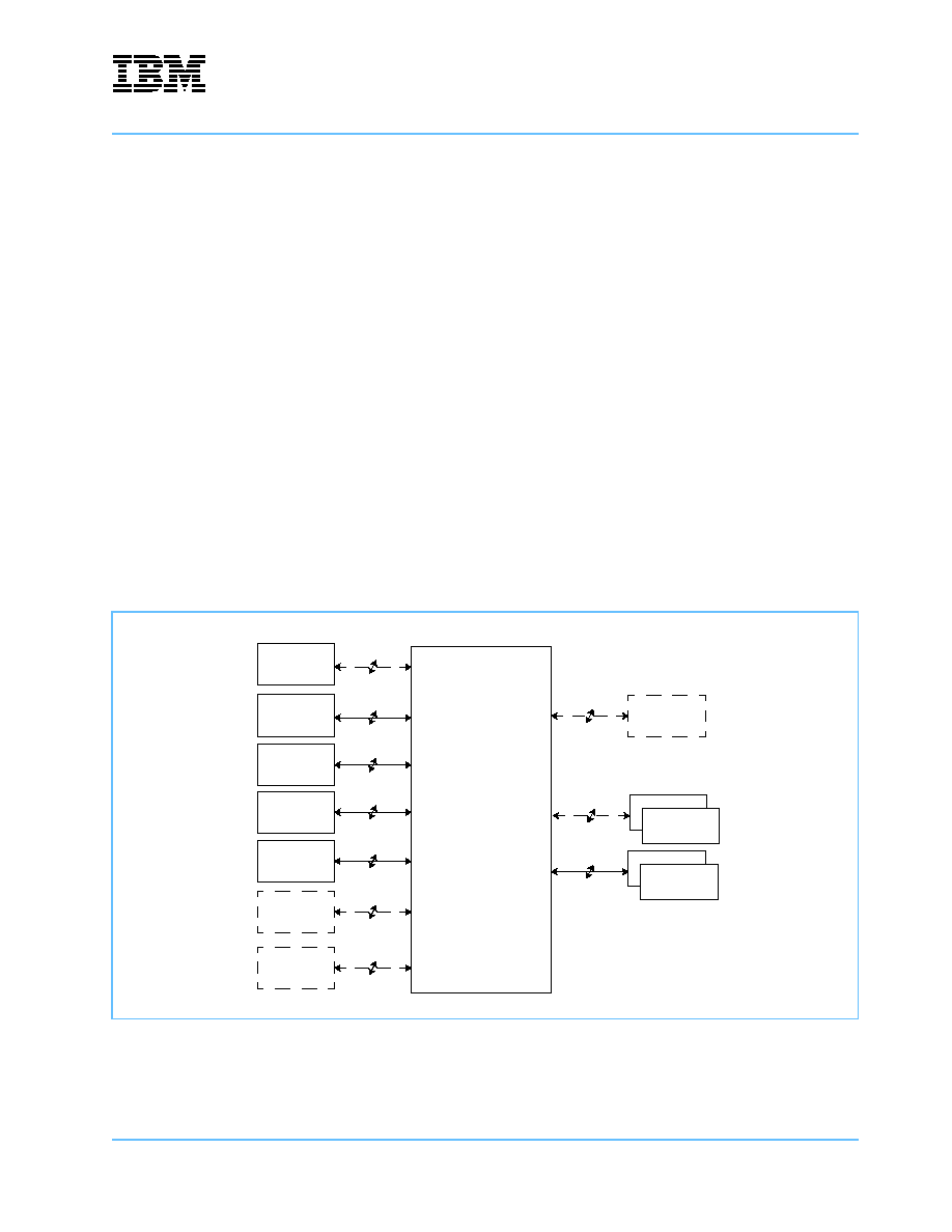
IBM PowerNP NP4GS3
Preliminary
Network Processor
np3_ds_sec13_config.fm.11
January 29, 2003
Configuration
Page 459 of 605
13. Configuration
The IBM PowerNP NP4GS3 Network Processor must be configured after internal diagnostics have run.
Configuration is performed by a control point function (CPF) that generates guided traffic to write configura-
tion registers. These configuration registers are reset by the hardware to a minimal option set.
The following sections describe all configuration registers and their reset state. A base address and offset are
provided.
13.1 Memory Configuration
The NP4GS3 is supported by a number of memory subsystems as shown in Figure 13-1. These memory
subsystems contain data buffers and controls used by the NP4GS3. The D0, D1, D2, D3, D4, DS_0, and
DS_1 subsystems are required to operate the NP4GS3 base configuration. Memory subsystems Z0, Z1, and
D6 are optional and provide additional functionality or capability when added to the required set of memory
subsystems.
In its base configuration, the NP4GS3 does not perform enhanced scheduling, and has a limited look-up
search capability. The enabling of memory subsystem interfaces is controlled by the contents of the Memory
Configuration Register (Memory_Config) (page 460). The bits in this register are set by hardware during reset
to enable the base configuration.
Figure 13-1. NP4GS3 Memory Subsystems
D4
NP4GS3
D6
Z0
D0
D3
57
51
33
48
51
DS0
51
DS1
D1
33
D2
33
51
Z1
39

IBM PowerNP NP4GS3
Network Processor
Preliminary
Configuration
Page 460 of 605
np3_ds_sec13_config.fm.11
January 29, 2003
13.1.1 Memory Configuration Register (Memory_Config)
The Memory Configuration Register (Memory_Config) enables or disables memory interfaces. It also enables
the egress scheduler and the Z1 memory interface required by the egress scheduler to operate.
Access Type
Read/Write
Base Address
x`A000 0120'
Reserved
CR
B
_
Ifc_en
able
Sch_Ena
Z0 D4 D3 D2 D1 D0
Reser
v
ed
D6
DS_1
DS_0
31 30 29 28 27 26 25 24 23 22 21 20 19 18 17 16 15 14 13 12 11 10
9
8
7
6
5
4
3
2
1
0
Field Name
Bits
Reset
Description
Reserved
31:13
Reserved.
CRB_Ifc_enable
12
0
When set to `1', enables the Coprocessor Response Bus (CRB) coproces-
sor external interface.
The Z0 Memory Subsystem Interface Enabled control (bit 9 of the Memory
Configuration Register (Memory_Config)) must also be set to `1' to enable
the CAB interface.
Sch_Ena
11:10
00
Scheduler Enabled control enables both egress scheduler and Z1 mem-
ory interface:
00
Scheduler disabled, Z1 interface disabled
01
Scheduler enabled, Z1 interface enabled
10
Scheduler disabled, Z1 interface enabled (NP4GS3B (R2.0) or
later)
11
Reserved
When enabling the scheduler, the target port queue count Qcnt_PQ must
be zero for all ports. When setting this value to `0', the target port queue
count (Qcnt_PQ) + free queue (FQ) must be zero for all ports.
Z0
9
0
Z0 Memory Subsystem Interface Enabled control:
1
Interface enabled
0
Interface disabled
D4
8
1
D4 Memory Subsystem Interface Enabled control:
1
Interface enabled
0
Interface disabled
D3
7
1
D3 Memory Subsystem Interface Enabled control:
1
Interface enabled
0
Interface disabled
D2
6
1
D2 Memory Subsystem Interface Enabled control:
1
Interface enabled
0
Interface disabled
D1
5
1
D1 Memory Subsystem Interface Enabled control:
1
Interface enabled
0
Interface disabled
D0
4
1
D0 Memory Subsystem Interface Enabled control:
1
Interface enabled
0
Interface disabled

IBM PowerNP NP4GS3
Preliminary
Network Processor
np3_ds_sec13_config.fm.11
January 29, 2003
Configuration
Page 461 of 605
Reserved
3
0
Reserved.
D6
2
0
D6 Memory Subsystem Interface Enabled control:
1
Interface enabled
0
Interface disabled
DS_1
1
1
DS_1 Memory Subsystem Interface Enabled control:
1
Interface enabled
0
Interface disabled
DS_0
0
1
DS_0 Memory Subsystem Interface Enabled control:
1
Interface enabled
0
Interface disabled
Field Name
Bits
Reset
Description
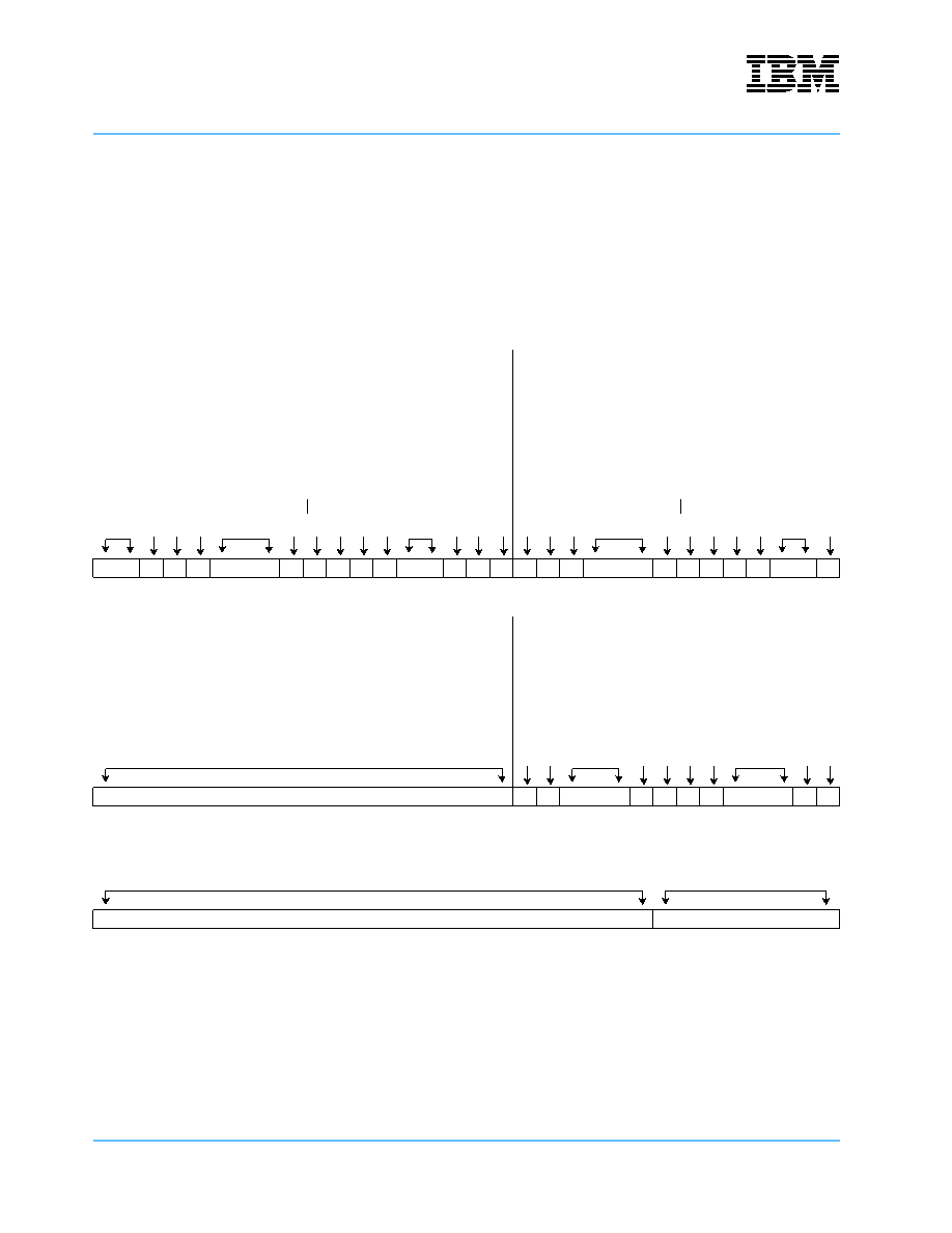
IBM PowerNP NP4GS3
Network Processor
Preliminary
Configuration
Page 462 of 605
np3_ds_sec13_config.fm.11
January 29, 2003
13.1.2 DRAM Parameter Register (DRAM_Parm)
The DRAM Parameter Register (DRAM_Parm) controls the operation of the dynamic random-access
memory (DRAM) used by the Embedded Processor Complex (EPC) and the Egress Enqueuer/Dequeuer/
Scheduler (EDS). Each DRAM is controlled separately.
Base Address Offset 0
Base Address Offset 1
NP4GS3C (R3.x)
Base Address Offset 2
Access Type
Read/Write
Base Address
x`A000 2400'
EPC_DRAM_Parms
EDS_DRAM_Parms
Strobe_cntl
Reserved
CS_Refresh_
R
ate
CS_Bank_R_W_Skip
CAS_
Latency
8_Bank_Ena
11/10
Drive_Strength
DLL_Disable
DQS
_
Clam
ping_Ena
DRAM_Size
FET_
Cntl_
E
n
a
Reserved
D0_Width
DS_D4_R
efresh_Rate
DS_Error_Che
cking
_
Disable
D4_Error_C
hecking_Disab
le
CAS_
Latency
8_Bank_Ena
11/10
Drive_Strength
DLL_Disable
DQS
_
Clam
ping_Ena
DRAM_Size
FET_
Cntl_
E
n
a
31 30 29 28 27 26 25 24 23 22 21 20 19 18 17 16 15 14 13 12 11 10
9
8
7
6
5
4
3
2
1
0
EPC_DRAM_Parms
D6_DRAM_Parms
Reserved
D6_R
efresh Rate
D6_Ban
k_R
W
_Skp
CAS_Late
n
cy
11/10
Drive_ Stre
ngth
DLL_
Disable
DQS_ Clamping_ Ena
D6_D
RAM_Size
FE
T_
C
n
t
l
_
E
n
a
D6_Parity_Mode
31 30 29 28 27 26 25 24 23 22 21 20 19 18 17 16 15 14 13 12 11 10
9
8
7
6
5
4
3
2
1
0
Reserved
Auto_precharge
31 30 29 28 27 26 25 24 23 22 21 20 19 18 17 16 15 14 13 12 11 10
9
8
7
6
5
4
3
2
1
0

IBM PowerNP NP4GS3
Preliminary
Network Processor
np3_ds_sec13_config.fm.11
January 29, 2003
Configuration
Page 463 of 605
Base Address Offset 0
Field Name
Bits
Reset
Description
Strobe_cntl
31:30
00
Strobe control for double data rate (DDR) DRAM interfaces:
00
Each DDR DRAM interface uses one strobe (xx_DQS) for each
byte of data lines.
01
D0, D1, D2, D3 DDR DRAM interface use one strobe (xx_DQS)
for each byte of data lines.
DS0, DS1, and D4 DDR DRAM interface use one strobe
(xx_DQS) for all data lines.
10
Reserved.
11
Reserved.
Note: The above is available in NP4GS3B (R2.0) or later.
Reserved
29
Reserved.
CS_Refresh_Rate
28
1
CS_Refresh_Rate. Controls the refresh rate for D0, D1, D2 and D3:
0
Double refresh rate (7.5
�s)
1
Normal refresh rate (15
�s)
CS_Bank_RW_Skp
27
0
Controls the number of banks that must be skipped within a DRAM
access window when switching from a read to a write:
0
Skip 1 bank
1
Skip 2 banks
The proper setting for this bit is related to the DRAM timing specifications
and the CAS_Latency value.
This control is for all Control Stores (D0, D1, D2, D3, D6).
CS_Bank_RW_Skp
(NP4GS3B (R2.0))
27
0
This bit controls the number of banks that must be skipped within a DRAM
access window when switching from a read to a write:
0
Skip 1 bank. CAS_Latency (bits 26:24) must be set to `010' to
support this option.
1
Skip 2 banks.
The proper setting for this bit is related to the times of the DRAM with
respect to the CAS_Latency value. This control is for D0, D1, D2 and D3
control stores.
CAS_Latency
26:24,
10:8
010
DRAM Column Address Strobe (CAS) Latency value corresponds to the
DRAM's read latency measured from the Column Address. (DDR DRAM
Mode Register, bits 6:4; see the DRAM documentation for more informa-
tion.)
000 - 001
Reserved
010
2 clock cycles (PC266A-compliant DRAMs)
011
3 clock cycles
100 - 101
Reserved
110
2.5 clock cycles (PC266B-compliant DRAMs)
111
Reserved
8_Bank_Enable
23, 7
0
Eight Bank Addressing Mode Enable control value. For proper operation,
must be set to `0'.
11/10
22, 6
1
Ten- or eleven-cycle DRAM control value controls the number of core
clock cycles the DRAM controller uses to define an access window:
0
10-cycle DRAM
1
11-cycle DRAM
Drive_Strength
21, 5
0
DRAM Drive Strength control. (DDR DRAM Extended Mode Register,
bit 1, see the DRAM documentation for more information.)
0
Strong
1
Weak

IBM PowerNP NP4GS3
Network Processor
Preliminary
Configuration
Page 464 of 605
np3_ds_sec13_config.fm.11
January 29, 2003
DLL_Disable
20, 4
0
Delay-locked loop (DLL) Disable control. For proper operation, must be
set to `0'. (DDR DRAM Extended Mode Register, bit 0, see the DRAM
documentation for more information.)
DQS_Clamping_Ena
19, 3
0
Data Q Strobe (DQS) Clamping Enable control. For proper operation,
must be set to `0'.
DRAM_Size
18:17
00
DRAM Size indicates the size of the Control Stores D0-D3 in DRAMs:
00
4x1Mx16 DDR DRAM, Burst = 4
01
4x2Mx16 DDR DRAM, Burst = 4
10
4x4Mx16 DDR DRAM, Burst = 4
11
Reserved
Note: D0 can also be configured to be double-wide (x32).
FET_Cntl_Ena
16, 0
0
Field-Effect Transistor (FET) Control Enable control. For proper operation,
must be set to `0'.
Reserved
15
Reserved.
D0_Width
14
1
D0 Width control indicates if one or two DRAMs are used for the D0 Con-
trol Store (CS):
0
Single-wide configuration using one DRAM. A single bank access
provides 64 bits of data.
1
Double-wide configuration using two DRAMs. A single bank
access provides 128 bits of data.
DS_D4_Refresh_Rate
13
0
Refresh rate control for DS0, DS1 and D4 (NP4GS3B (R2.0)):
0
Normal refresh rate (15
�s)
1
Double refresh rate (7.5
�s)
DS_Error_Checking_Disable
12
0
Egress Data Store Error Checking Disable control. When this field is set to
`1', all DRAM error checking for the egress data store is disabled.
D4_Error_Checking_Disable
11
0
D4 DRAM Error Checking Disable. When this field is set to `1', all DRAM
error checking for the D4 DRAM is disabled.
DRAM_Size
2:1
00
DRAM Size indicates the size of the Egress Data Store (DS0 and DS1)
and D4 DRAMs:
00
4 x 1 M x 16 DDR DRAM x 2 (or 4 x 1 M x 32 DDR DRAM x 1)
01
4 x 2 M x 16 DDR DRAM x 2 (or 4 x 2 M x 32 DDR DRAM x 1)
10
4 x 4 M x 16 DDR DRAM x 2 (or 4 x 4 M x 32 DDR DRAM x 1)
11
4 x 512 K x 32 DDR DRAM x 1
The setting of this field affects the size of the extended stack queuesas
follows:
GQ
00
01
10
11
GTQ
48 K
96 K
192 K
24 K
GPQ
48 K
96 K
192 K
24 K
GFQ
192 K
384 K
768 K
96 K
GR0
96 K
192 K
384 K
48 K
GR1
96 K
192 K
384 K
48 K
GB0
96 K
192 K
384 K
48 K
GB1
96 K
192 K
384 K
48 K
Discard 96 K
192 K
384 K
48 K
Field Name
Bits
Reset
Description

IBM PowerNP NP4GS3
Preliminary
Network Processor
np3_ds_sec13_config.fm.11
January 29, 2003
Configuration
Page 465 of 605
Base Address Offset 1
Field Name
Bit(s)
Reset
Description
Reserved
31:14
Reserved.
D6_Refresh_Rate
13
0
This field controls the refresh rate for D6:
0
Normal refresh rate (15
�s)
1
Double refresh rate (7.5
�s)
D6_Bank_RW_Skp
12
0
This controls the number of banks that must be skipped within a DRAM
access window when switching from a read to a write:
0
Skip 1 bank. CAS_Latency (bits11:9) must be set to '010' to sup-
port this option.
1
Skip 2 banks.
The proper setting for this is related to the DRAM timing specifications
and the CAS_Latency value. This control is for D6 only.
CAS_Latency
11:9
010
DRAM Column Address Strobe Latency value corresponds to the DRAM's
read latency measured from the Column Address. (DDR DRAM Mode
Register, bits 6:4; see the DRAM documentation for more information.)
000 - 001
Reserved
010
2 clock cycles (PC266A-compliant DRAMs)
011
3 clock cycles
100 - 101
Reserved
110
2.5 clock cycles (PC266B-compliant DRAMs)
111
Reserved
11/10
8
0
Ten- or eleven-cycle DRAM control value controls the number of core
clock cycles the DRAM controller uses to define an access window:
0 10-cycle
DRAM
1 11-cycle
DRAM
Drive_Strength
7
0
DRAM Drive Strength control. (DDR DRAM Extended Mode Register,
bit 1, see the DRAM documentation for more information.)
0
Strong
1
Weak
DLL_Disable
6
0
DLL Disable control. For proper operation, must be set to `0'. (DDR DRAM
Extended Mode Register, bit 0, see the DRAM documentation for more
information.)
DQS_Clamping_Ena
5
0
DQS Clamping Enable control. For proper operation, must be set to `0'.
D6_DRAM_Size
4:2
110
Indicates the size of the D6 DRAM:
000
4x1Mx16
001
4x2Mx16
010
4x4Mx16
011
Reserved
100
4x4Mx4
101
4x8Mx4
110
4x16Mx4
111
Reserved
FET_Cntl_Ena
1
0
FET Control Enable control. For proper operation, must be set to `0':
D6_Parity_Mode
0
1
DRAM D6 Parity Mode Disable control value:
0
D6 interface supports an additional two DDR DRAMs which sup-
port byte parity. The hardware generates on write and checks
parity on read.
1
D6 interface does not support parity.

IBM PowerNP NP4GS3
Network Processor
Preliminary
Configuration
Page 466 of 605
np3_ds_sec13_config.fm.11
January 29, 2003
NP4GS3C (R3.x)
Base Address Offset 2
Field Name
Bit(s)
Reset
Description
Reserved
31:8
Reserved.
Auto_precharge
7:0
0
Configures the address bit used to flag the auto precharge operation for
the attached DDR DRAM. When set to `0', A10 is used. When set to `1',
A8 is used.
Bit
DRAM Interface
7
DS1
6
DS0
5
D6
4
D4
3
D3
2
D2
1
D1
0
D0
The NP4GS3B (R2.0) does not provide this configuration and uses only
A10 to flag the auto precharge operation.

IBM PowerNP NP4GS3
Preliminary
Network Processor
np3_ds_sec13_config.fm.11
January 29, 2003
Configuration
Page 467 of 605
13.1.3 Delay Calibration Registers (NP4GS3C (R3.x))
These registers are used to modify the interface timings for the DDR interfaces. These registers can be used
to initialize the output multiplier fields in the following offsets to x'6A'. Otherwise, these registers should be
modified only when directed by an IBM field engineer.
Base Address Offset 0 (R/W) (D0, D1, D2, D3, D4, D6, DS0, and DS1)
Access Type
Base Address Offset 0
Base Address Offset 2
Base Address Offset 4
Base Address Offset 6
Base Address Offset 8
Base Address Offset 10
Base Address Offset 12
Base Address Offset 15
Read/Write
Base Address Offset 1
Base Address Offset 3
Base Address Offset 5
Base Address Offset 7
Base Address Offset 9
Base Address Offset 11
Base Address Offset 13
Read Only
Base Address
D0_DDR_DCR
x`A080 0010'
D1_DDR_DCR
x`A080 0020'
D2_DDR_DCR
x`A080 0040'
D3_DDR_DCR
x`A080 0080'
D4_DDR_DCR
x`A080 0100'
D6_DDR_DCR
x`A080 0200'
DS0_DDR_DCR
x`A080 0400'
DS1_DDR_DCR
x`A080 0800'
Reserved
Outpu
t
Ov
err
i
de
V
a
li
d
Output override value
Output offset
Output multiplier
31 30 29 28 27 26 25 24 23 22 21 20 19 18 17 16 15 14 13 12 11 10
9
8
7
6
5
4
3
2
1
0

IBM PowerNP NP4GS3
Network Processor
Preliminary
Configuration
Page 468 of 605
np3_ds_sec13_config.fm.11
January 29, 2003
Base Address Offset 1 (RO) (D0, D1, D2, D3, D4, D6, DS0, and DS1)
Base Address Offset 2, N = 0 (R/W) (D0, D1, D2, D3, D4, D6, DS0, DS1)
Base Address Offset 4, N = 1 (R/W) (D0, D1, D2, D3, D4, D6, DS0, DS1)
Base Address Offset 6, N = 2 (R/W) (D0, D4, D6, DS0, DS1)
Base Address Offset 8, N = 3 (R/W) (D0, D4, D6, DS0, DS1)
Base Address Offset 3, N = 0 (RO) (D0, D1, D2, D3, D4, D6, DS0, DS1)
Base Address Offset 5, N = 1 (RO) (D0, D1, D2, D3, D4, D6, DS0, DS1)
Base Address Offset 7, N = 2 (RO) (D0, D4, D6, DS0, DS1)
Base Address Offset 9, N = 3 (RO) (D0, D4, D6, DS0, DS1)
Reserved
Calibratio
n error
Ou
tput delay o
v
errun
Raw delay
31 30 29 28 27 26 25 24 23 22 21 20 19 18 17 16 15 14 13 12 11 10
9
8
7
6
5
4
3
2
1
0
Reserved
Strobe
N
input override valid
Strobe N input
override value
Strobe N input offset
31 30 29 28 27 26 25 24 23 22 21 20 19 18 17 16 15 14 13 12 11 10
9
8
7
6
5
4
3
2
1
0
Reserved
Strobe
N
input de
lay overru
n
Strobe N input
calculated delay
31 30 29 28 27 26 25 24 23 22 21 20 19 18 17 16 15 14 13 12 11 10
9
8
7
6
5
4
3
2
1
0

IBM PowerNP NP4GS3
Preliminary
Network Processor
np3_ds_sec13_config.fm.11
January 29, 2003
Configuration
Page 469 of 605
Base Address Offset 10, N = 0 (R/W) (D6)
Base Address Offset 12, N = 1 (R/W) (D6)
Base Address Offset 11, N = 0 (RO) (D6)
Base Address Offset 13, N = 1 (RO) (D6)
Base Address Offset 15 (R/W) (D0, D1, D2, D3, D4, D6, DS0, DS1)
Base Address Offset 0 (R/W) (D0, D1, D2, D3, D4, D6, DS0, and DS1)
Reserved
Strobe Par
N
inp
u
t ove
rride valid
Strobe Par N input
override value
Strobe Par N input offset
31 30 29 28 27 26 25 24 23 22 21 20 19 18 17 16 15 14 13 12 11 10
9
8
7
6
5
4
3
2
1
0
Reserved
Strobe Par
N
inp
u
t delay overrun
Strobe Par N input
calculated delay
31 30 29 28 27 26 25 24 23 22 21 20 19 18 17 16 15 14 13 12 11 10
9
8
7
6
5
4
3
2
1
0
Reserved
Common strobe
input multiplier
31 30 29 28 27 26 25 24 23 22 21 20 19 18 17 16 15 14 13 12 11 10
9
8
7
6
5
4
3
2
1
0
Field Name
Bit(s)
Reset
Description
Reserved
31:25
Reserved.
Output Override Valid
24
0
Output override valid.
Output override value
23:16
0
Output override value.
Output offset
15:8
0
Output offset.
Output multiplier
7:0
x`35'
Output multiplier. Prior to initializing the DDR DRAMs, this field must be
written to a value of x`6A'.

IBM PowerNP NP4GS3
Network Processor
Preliminary
Configuration
Page 470 of 605
np3_ds_sec13_config.fm.11
January 29, 2003
Base Address Offset 1 (RO) (D0, D1, D2, D3, D4, D6, DS0, and DS1)
Base Address Offset 2, N = 0 (R/W) (D0, D1, D2, D3, D4, D6, DS0, DS1)
Base Address Offset 4, N = 1 (R/W) (D0, D1, D2, D3, D4, D6, DS0, DS1)
Base Address Offset 6, N = 2 (R/W) (D0, D4, D6, DS0, DS1)
Base Address Offset 8, N = 3 (R/W) (D0, D4, D6, DS0, DS1)
Base Address Offset 3, N = 0 (RO) (D0, D1, D2, D3, D4, D6, DS0, DS1)
Base Address Offset 5, N = 1 (RO) (D0, D1, D2, D3, D4, D6, DS0, DS1)
Base Address Offset 7, N = 2 (RO) (D0, D4, D6, DS0, DS1)
Base Address Offset 9, N = 3 (RO) (D0, D4, D6, DS0, DS1)
Base Address Offset 10, N = 0 (R/W) (D6)
Base Address Offset 12, N = 1 (R/W) (D6)
Field Name
Bit(s)
Reset
Description
Reserved
31:10
Reserved.
Calibration error
9
0
Calibration error.
Output delay overrun
8
0
Output delay overrun.
Raw delay
7:0
0
Raw delay.
Field Name
Bit(s)
Reset
Description
Reserved
31:17
Reserved.
Strobe N input override valid
16
0
Strobe N input override valid.
Strobe N input override
15:8
0
Strobe N input override value.
Strobe N input offset
7:0
0
Strobe N input offset.
Field Name
Bit(s)
Reset
Description
Reserved
31:9
Reserved.
Strobe N input delay
overrun
8
0
Strobe N input delay overrun.
Strobe N input
calculated delay
7:0
0
Strobe N input calculated delay.
Field Name
Bit(s)
Reset
Description
Reserved
31:17
Reserved.
Strobe Par N input
override valid
16
0
Strobe Par N input override valid.
Strobe Par N input
override value
15:8
0
Strobe Par N input override value.
Strobe Par N input offset
7:0
0
Strobe Par N input offset.

IBM PowerNP NP4GS3
Preliminary
Network Processor
np3_ds_sec13_config.fm.11
January 29, 2003
Configuration
Page 471 of 605
Base Address Offset 11, N = 0 (RO) (D6)
Base Address Offset 13, N = 1 (RO) (D6)
Base Address Offset 15 (R/W) (D0, D1, D2, D3, D4, D6, DS0, DS1)
Field Name
Bit(s)
Reset
Description
Reserved
31:9
Reserved.
Strobe Par N input
delay overrun
8
0
Strobe Par N input delay overrun.
Strobe Par N input
calculated delay
7:0
0
Strobe Par N input calculated delay.
Field Name
Bit(s)
Reset
Description
Reserved
31:8
Reserved.
Common strobe input
multiplier
7:0
x`6A'
Common strobe input multiplier.

IBM PowerNP NP4GS3
Network Processor
Preliminary
Configuration
Page 472 of 605
np3_ds_sec13_config.fm.11
January 29, 2003
13.2 Master Grant Mode Register (MG_Mode)
This configuration register configures the Master Grant I/O (MGrant_A, MGrant_B) for either nested priority or
independent priority mode.
Access Type
Read/Write
Base Address
x'A000 0820'
Reserved
MG_
M
ode
31 30 29 28 27 26 25 24 23 22 21 20 19 18 17 16 15 14 13 12 11 10
9
8
7
6
5
4
3
2
1
0
Field Name
Bit(s)
Reset
Description
Reserved
31:1
Reserved.
MG_Mode
0
0
0
The MGrant I/O is defined for nested priority encoding which is
defined as:
00
No grant (on any priority)
01
Priority 0 has grant
10
Priorities 0 and 1 have grant
11
Priorities 0, 1, and 2 have grant
1
The MGrant I/O is defined for independent priority encoding
which is defined as:
00
No grant (on any priority)
01
Priority 0 and 1 have grant
10
Priority 2 has grant
11
Priority 0, 1, and 2 have grant

IBM PowerNP NP4GS3
Preliminary
Network Processor
np3_ds_sec13_config.fm.11
January 29, 2003
Configuration
Page 473 of 605
13.3 TB Mode Register (TB_Mode)
The target blade mode configures the maximum number of target network processors supported.
Offset 1controls the toggle mode operation configuration.
Base Address Offset 0
NP4GS3C (R3.x)
Base Address Offset 1
NP4GS3C (R3.x)
Base Address Offset 2
Base Address Offset 0
Access Type
Read/Write
Base Address
x'A000 0410'
Reserved
TB_Mode
31 30 29 28 27 26 25 24 23 22 21 20 19 18 17 16 15 14 13 12 11 10
9
8
7
6
5
4
3
2
1
0
Reserved
T
oggle Mode
31 30 29 28 27 26 25 24 23 22 21 20 19 18 17 16 15 14 13 12 11 10
9
8
7
6
5
4
3
2
1
0
Reserved
BCI_F
o
rmat_Ct
l
31 30 29 28 27 26 25 24 23 22 21 20 19 18 17 16 15 14 13 12 11 10
9
8
7
6
5
4
3
2
1
0
Field Name
Bit(s)
Reset
Description
Reserved
31:2
Reserved.
TB_Mode
1:0
00
Target Blade Mode. This field is used to define the target blade mode cur-
rently in use by the NP4GS3. The field is defined as:
00
16 blade mode. Valid addresses are 0:15. Multicast is indicated
as a 16-bit vector.
01
32 blade mode. Valid unicast target blade field encodes are 0
through 31. Multicast encodes are in the range of 512 through
65535.
10
64 blade mode. Valid unicast target blade field encodes are 0
through 63. Multicast encodes are in the range of 512 through
65535.
11
Reserved

IBM PowerNP NP4GS3
Network Processor
Preliminary
Configuration
Page 474 of 605
np3_ds_sec13_config.fm.11
January 29, 2003
NP4GS3C (R3.x)
Base Address Offset 1
NP4GS3C (R3.x)
Base Address Offset 2
Field Name
Bit(s)
Reset
Description
Reserved
31:1
Reserved.
Toggle Mode
0
0
Enables the toggle mode.
0
Enables egress data store standard mode operation. Places
frame data into DS0, DS1, or both data stores. Data storage unit
(DSU) information fields indicate the following:
Two-Bit DSU Information Field
00
Reserved
01
DS0
10
DS1
11
DS0 and DS1
One-Bit DSU Information Field
0
DS0
1
DS1
1
Enables egress data store toggle mode operation. Places frame
data into DS0 and DS1 according to the twin format. DSU infor-
mation fields indicate the following:
Two-Bit DSU Information Field
00
Invalid
01
Twin format 0
10
Twin format 1
11
Invalid
One-Bit DSU Information Field
0
Twin format 0
1
Twin format 1
Field Name
Bit(s)
Reset
Description
Reserved
31:1
Reserved.
BCI_Format_Ctl
0
0
Controls the format of the byte count information (BCI) used in the egress
frame control block page (FCBPage). The BCI is located at word 1
(FCBPage byte offsets 4 through 7) of the FCBPage. See
Section 7.4.4 Enqueue Coprocessor on page 247.
0
Compact format:
Bits
Description
31:20
Reserved
19:14 Starting
byte
13:6
Number of data buffers (weight)
5:0 Ending
byte
1
Expanded format:
Bits
Description
31:22
Reserved
21:16 Starting
byte
15:8
Number of data buffers (weight)
7:6
Reserved
5:0 Ending
byte

IBM PowerNP NP4GS3
Preliminary
Network Processor
np3_ds_sec13_config.fm.11
January 29, 2003
Configuration
Page 475 of 605
13.3.1 Toggle Mode
The toggle mode provides increased bandwidth to egress data stores by changing the data storage method.
The toggle mode is activated by configuring the corresponding field in offset 1 of the TB Mode Register
(TB_Mode) (page 473). All Data Mover Unit (DMU) modes are supported.
When the toggle mode is inactive, frame data is assigned to DS0, DS1, or both data stores. Bandwidth limita-
tions occur when there is a consistent requirement for data to be stored in both data stores, such as with
multicast and guided traffic, and when the NP4GS3 is configured for OC-48 ports.
The toggle mode changes the data storage method by defining a "twin" format for use by all twins assigned to
a frame. Unicast, multicast, and guided traffic frames are all assigned in the same manner. When the toggle
mode is active, multicast and guided frames are assigned a twin format so that they are not written into both
data stores. DSU settings found in the frame header are ignored; the twin format controls which data store is
used for reading and writing.
The twin format is assigned when the first frame buffer is loaded into the data store. For unpacked frames,
the assignment toggles between formats at each start of frame. For packed frames, the assignment is based
on the current write window.
Two twin formats are defined:
� Twin format 0. The even buffer is located in DS0 and the odd buffer is located in DS1.
� Twin format 1. The even buffer is located in DS1 and the odd buffer is located in DS0.
For packed frames, assignment is based on where the current frame is written. This definition allows the
entire packed cell (end of current frame and start of next frame) to be stored during the current write window:
Current Frame Data Store
Next Frame Format
0
0
1
1
13.3.1.1 DSU information
The NP4GS3 passes the DSU information that originates from the frame header to the general queues (GR0,
GR1, GB0, GB1, GFQ, GPQ, and GTQ), dispatch unit, data store coprocessor, FCBPage, discard queue,
and common FCB. With the exception of the frame header DSU field, the various fields employed for this
purpose are reused (when the toggle mode is active) to indicate the frame's assigned format.
When the toggle mode is active, a two-bit DSU information field is defined as follows:
00
Invalid
01
Twin format 0
10
Twin format 1
11
Invalid
When the toggle mode is active, a one-bit DSU information field is defined as follows:
0
Twin format 0
1
Twin format 1

IBM PowerNP NP4GS3
Network Processor
Preliminary
Configuration
Page 476 of 605
np3_ds_sec13_config.fm.11
January 29, 2003
An example of a one-bit DSU field is the Type(0) field found in the general queues (GR0, GR1, GB0, GB1,
GFQ, GPQ, and GTQ). To maintain the frame order in general data queues (GR0, GR1, GB0, and GB1), the
low-order bit of the source blade (SB) is used to select the queue as follows:
SB(0)
GRx, GBx selected
0
GR1, GB1
1
GR0, GR0
This bit allows the use of all egress general data queues without a loss in frame order.
Note: Dispatch port configuration table (PCT) entries 48 and 49 should be identical when the toggle mode is
enabled because no information can be inferred about the frame other than the twin format.
Because the frame header DSU field is not used when the toggle mode is active, the egress FCBPage DSU
field and the Disp_DSU field (both two-bit DSU information fields) are initialized based on the value of
Type(0):
Type(0)
FCBPage DSU, Disp_DSU
0
01
1
10
The DSControl field (a two-bit DSU information field) in the WREDS, RDEDS, RDMOREE, and EDIRTY data
store coprocessor commands indicate data store use. When the toggle mode is active, the DSControl field
determines the format of the twins being written:
00
Uses the Disp_DSU value captured at dispatch
01
Forces twin format 0
10
Forces twin format 1
11
Invalid
Disp_DSU conforms to the definition of a two-bit DSU information field.
For the Egress General Data Queue (E-GDQ), Type(1:0) indicates the twin format used and conforms to the
two-bit DSU field definition above.
13.3.1.2 ENQE Command and Qclass 5 or 6
When the toggle mode is inactive, the general data queue selected (GR0, GR1, GB0, or GB1) is based on the
value of QID(2:0), where QID(0) is set to the DSUSel value. When the toggle mode is active, the low-order bit
of the FCBPage SB field is used as follows:
SB(0)
GRx, GBx selected
0
GR1, GB1
1
GR0, GR0
This bit value matches the selection made when the enqueue to the general data queues is performed as
described above.
IBM PowerNP NP4GS3
Preliminary
Network Processor
np3_ds_sec13_config.fm.11
January 29, 2003
Configuration
Page 477 of 605
13.4 Egress Reassembly Sequence Check Register (E_Reassembly_Seq_Ck)
This configuration register enables sequence checking by the egress reassembly logic. The sequence
checking ensures that start of frame, optional middle of frame, and end of frame indications occur in the
expected order for each cell of a frame being reassembled. Each cell that does not indicate start or end of
frame carries a sequence number that is checked for proper order.
Access Type
Read/Write
Base Address
x'A000 0420'
Reserved
Seq
_
Chk_Ena
31 30 29 28 27 26 25 24 23 22 21 20 19 18 17 16 15 14 13 12 11 10
9
8
7
6
5
4
3
2
1
0
Field Name
Bit(s)
Reset
Description
Reserved
31:1
Reserved.
Seq_Chk_Ena
0
1
Sequence Check Enable control:
0
Sequence checking disabled
1
Sequence checking enabled for the E_EDS

IBM PowerNP NP4GS3
Network Processor
Preliminary
Configuration
Page 478 of 605
np3_ds_sec13_config.fm.11
January 29, 2003
13.5 Aborted Frame Reassembly Action Control Register (AFRAC)
This configuration register controls the action the hardware takes on a frame whose reassembly was aborted
due to the receipt of an abort command in a cell header for the frame.
Access Type
Read/Write
Base Address
x'A000 0440'
Reserved
AFRAC
31 30 29 28 27 26 25 24 23 22 21 20 19 18 17 16 15 14 13 12 11 10
9
8
7
6
5
4
3
2
1
0
Field Name
Bit(s)
Reset
Description
Reserved
31:1
Reserved.
AFRAC
0
0
Aborted Frame Reassembly Action Control:
0
Aborted frames are enqueued to the Discard Queue.
1
Aborted frames are enqueued with other frames on the associ-
ated GQ.

IBM PowerNP NP4GS3
Preliminary
Network Processor
np3_ds_sec13_config.fm.11
January 29, 2003
Configuration
Page 479 of 605
13.6 Packing Registers
13.6.1 Packing Control Register (Pack_Ctrl)
This configuration register is used to enable the transmission of packed cells across the switch interface.
When enabled, the ingress Switch Data Mover (I-SDM) determines if there is available space in the current
cell being prepared for transmission and if there is an available packing candidate. A frame can be packed
only if it is unicast, has the same target blade destination as the current frame, and is longer than 48 bytes.
The packed frame starts on the next quadword (QW) boundary following the last byte of the current frame.
This control does not affect the ability of the E_EDS to receive packed cells.
Access Type
Read/Write
Base Address
x'A000 0480'
Reserved
Pack_Ena
31 30 29 28 27 26 25 24 23 22 21 20 19 18 17 16 15 14 13 12 11 10
9
8
7
6
5
4
3
2
1
0
Field Name
Bit(s)
Reset
Description
Reserved
31:1
Reserved.
Pack_Ena
0
1
Packing Enabled flag:
0
Cell packing disabled
1
Cell packing enabled

IBM PowerNP NP4GS3
Network Processor
Preliminary
Configuration
Page 480 of 605
np3_ds_sec13_config.fm.11
January 29, 2003
13.6.2 Packing Delay Register (Pack_Dly) (NP4GS3B (R2.0))
The Packing Delay Register (Pack_Dly) (NP4GS3B (R2.0)) is used to modify the ingress scheduler actions
by the use of programmable wait periods per target blade (TB) based on source port (SP) media speed, as
determined by the DM_Bus_mode setting (see Data Mover Unit (DMU) Configuration Registers [page 531]).
During processing of a frame for transmission across the switch interface, when it is determined that the next
service will be the last for the frame and if there is no packing candidate at that time, then the selected TB run
queue is not included in subsequent service selections. A timer is used per TB run queue to keep the queue
out of the service selection until either the timer expires or a packing candidate (the corresponding start-of-
frame [SOF] ring goes from empty to nonempty) is available.
Frames from the wrap DMU are not affected by this mechanism. Multicast frames (which include guided
traffic) and the discard queues are not affected by this mechanism.
This function is disabled by setting the packing delay to `0'.
Access Type
Read/Write
Base Address
x'A020 8000'
Reserved
OC3_Delay OC12_Delay
FastEn_Delay
Gb_Delay
OC48_Delay
31 30 29 28 27 26 25 24 23 22 21 20 19 18 17 16 15 14 13 12 11 10
9
8
7
6
5
4
3
2
1
0
Field Name
Bit(s)
Reset
Description
Reserved
31:20
Reserved.
OC3_Delay
19:16
0
Maximum packing delay in units of 3840 ns.
OC12_Delay
15:12
0
Maximum packing delay in units of 960 ns.
FastEn_Delay
11:8
0
Maximum packing delay in units of 4800 ns.
Gb_Delay
7:4
0
Maximum packing delay in units of 480 ns.
OC48_Delay
3:0
0
Maximum packing delay in units of 240 ns.

IBM PowerNP NP4GS3
Preliminary
Network Processor
np3_ds_sec13_config.fm.11
January 29, 2003
Configuration
Page 481 of 605
13.7 Initialization Control Registers
13.7.1 Initialization Register (Init)
This register controls the initialization of the functional islands. Each functional island and the DRAM Control-
lers begin initialization when the bits in this register are set to `1'. Each functional island signals the successful
completion of initialization by setting its bit in the Initialization Done Register (Init_Done) (page 482). Once a
functional island has been initialized, changing the state of these bits will no longer have any effect until a
reset occurs.
Access Type
Read/Write
Base Address
x`A000 8100'
DMU_Init
Fu
nctional_Island_
Init
DRAM_C
n
tl_
S
ta
rt
Reserved
D
C
B
A
31 30 29 28 27 26 25 24 23 22 21 20 19 18 17 16 15 14 13 12 11 10
9
8
7
6
5
4
3
2
1
0
Field Name
Bit(s)
Reset
Description
DMU_Init
31:28
0000
Data Mover Unit Initialization control individually initializes each DMU.
Functional_Island_Init
27
0
Functional Island Initialization control:
0
No operation (nop)
1
Functional islands start hardware initialization. Completion of
hardware initialization is reported in the Initialization Done Regis-
ter (Init_Done).
DRAM_Cntl_Start
26
0
DRAM Controller Start Control:
0
Nop
1
Causes the DRAM Controllers to initialize and start operation.
When initialization completes, the DRAM controllers set the
CS_Init_Done and E-DS Init Done bits of the Initialization Done
Register (Init_Done).
Reserved
25:0
Reserved.

IBM PowerNP NP4GS3
Network Processor
Preliminary
Configuration
Page 482 of 605
np3_ds_sec13_config.fm.11
January 29, 2003
13.7.2 Initialization Done Register (Init_Done)
This register indicates that functional islands have completed their initialization when the corresponding bits
are set to `1'. This register tracks the initialization state of the functional islands. The Guided Frame Handler
(GFH) reads this register during the initialization of the NP4GS3.
Access Type
Read Only
Base Address
x`A000 8200'
E_Sched
_Init_
Done
DMU_Init_Done
I_EDS_Init_Done
Reserved
EPC_Init_Done
Reserved
CS_Init_Done
E_DS_Init_Done
E_EDS_Init_Done
Reserved
Reserved
P_DASL_Init_Done
A_DASL_Init_Done
Reserved
D
C
B
A
W
31 30 29 28 27 26 25 24 23 22 21 20 19 18 17 16 15 14 13 12 11 10
9
8
7
6
5
4
3
2
1
0
Field Name
Bit(s)
Reset
Description
E_Sched_Init_Done
31
0
Set to `1' by the hardware when the egress scheduler hardware com-
pletes its initialization.
DMU_Init_Done
30:26
0
Set to `1' by the hardware when the DMU hardware has completed its ini-
tialization.
Bit
DMU
30
D
29
C
28
B
27
A
26
Wrap
I_EDS_Init_Done
25
0
Set to `1' by the hardware when the Ingress EDS completes its
initialization.
Reserved
24
Reserved.
EPC_Init_Done
23
0
Set to `1' by the hardware when the EPC completes its initialization.
Reserved
22
Reserved.
CS_Init_Done
21
0
Set to `1' by the hardware when the Control Store's DRAM controller com-
pletes its initialization.
E_DS_Init_Done
20
0
Set to `1' by the hardware when the Egress Data Stores' DRAM controller
completes its initialization.
E_EDS_Init_Done
19
0
Set to `1' by the hardware when the Egress EDS completes its
initialization
Reserved
18:17
Reserved.
P_DASL_Init_Done
16
0
Set to `1' by the hardware when the primary data-aligned synchronous link
(DASL) completes its initialization. The DASL interface continues to send
synchronization cells.
A_DASL_Init_Done
15
0
Set to `1' by the hardware when the alternate DASL completes its initial-
ization. The DASL interface continues to send synchronization cells.
Reserved
14:0
Reserved.
IBM PowerNP NP4GS3
Preliminary
Network Processor
np3_ds_sec13_config.fm.11
January 29, 2003
Configuration
Page 483 of 605
13.8 NP4GS3 Ready Register (NPR_Ready)
Access Type
Read/Write
Base Address
x`A004 0020'
Rea
d
y
Reserved
31 30 29 28
27 26 25 24 23 22 21 20 19
18 17 16 15 14 13 12 11 10
9
8
7
6
5
4
3
2
1
0
Field Name
Bit(s)
Reset
Description
Ready
31
0
Ready is configured by picocode to drive a chip pin to indicate that the
NP4GS3 has been initialized and is ready to receive Guided Traffic:
0
NP4GS3 not ready
1
NP4GS3 ready
Reserved
30:0
Reserved.

IBM PowerNP NP4GS3
Network Processor
Preliminary
Configuration
Page 484 of 605
np3_ds_sec13_config.fm.11
January 29, 2003
13.9 Phase-Locked Loop Registers
13.9.1 Phase-Locked Loop Fail Register (PLL_Lock_Fail)
Access Type
Read Only
Base Address
x`A000 0220'
Reserved
Pl
lc
_l
ock_fai
l
ed
Pllb_lock_failed
Plla_lock_failed
PLL_C_Lock
PLL_B_Lock
PLL_A_Lock Fail
31 30 29 28 27 26 25 24 23 22 21 20 19 18 17 16 15 14 13 12 11 10
9
8
7
6
5
4
3
2
1
0
Field Name
Bit(s)
Reset
Description
Reserved
31:7
Reserved.
Pllc_lock_failed
6
Pllc_lock_failed.
0
Pllc has stayed correctly locked continuously since the last reset.
1
Pllc has lost lock. (Lock was lost any time since the last reset.)
Pllb_lock_failed
5
Pllb_lock_failed.
0
Pllb has stayed correctly locked continuously since the last reset.
1
Pllb has lost lock. (Lock was lost any time since the last reset.)
Plla_lock_failed
4
Plla_lock_failed.
0
Plla has stayed correctly locked continuously since the last reset.
1
Plla has lost lock. (Lock was lost any time since the last reset.)
PLL_C_Lock
3
Current status of lock indicator of the Core Clock PLL:
0
Phase/frequency lock
1
Phase/frequency seek
PLL_B_Lock
2
Current status of lock indicator of the DASL-B PLL:
0
Phase/frequency lock
1
Phase/frequency seek
PLL_A_Lock
1
Current status of lock indicator of the DASL-A PLL:
0
Phase/frequency lock
1
Phase/frequency seek
Fail
0
Phase-Locked Loop Fail indicator - indicates that an on-chip PLL has
failed. This field is written by the clock logic.
0
PLLs OK
1
PLL failed
If Fail is indicated at the end of the reset interval (101
�s after reset is
started) the operational device I/O is set to `1'. After the end of the reset
interval, a change in Fail will not affect operational device I/O.
Note: For NP4GS3B (R2.0), the operational device I/O is not affected by
the above.

IBM PowerNP NP4GS3
Preliminary
Network Processor
np3_ds_sec13_config.fm.11
January 29, 2003
Configuration
Page 485 of 605
13.10 Software Controlled Reset Register (Soft_Reset)
This register provides a control for software to reset the network processor.
Access Type
Write Only
Base Address
x`A000 0240'
F
u
ll_Reset
Reserved
31 30 29 28 27 26 25 24 23 22 21 20 19 18 17 16 15 14 13 12 11 10
9
8
7
6
5
4
3
2
1
0
Field Name
Bit(s)
Reset
Description
Full_Reset
31
0
Full Reset value resets the NP4GS3 hardware via the picocode. This is
the same full reset function provided by the Blade_Reset I/O.
0
Reserved
1
NP4GS3 performs an internal hardware reset
Reserved
30:0
Reserved.

IBM PowerNP NP4GS3
Network Processor
Preliminary
Configuration
Page 486 of 605
np3_ds_sec13_config.fm.11
January 29, 2003
13.11 Ingress Free Queue Threshold Configuration
13.11.1 BCB_FQ Threshold Registers
The value of the queue count in the BCB_FQ Control Block is continuously compared to the values each of
the three threshold registers contains. The result of this comparison affects the NP4GS3's flow control mech-
anisms. The values in these registers must be chosen such that BCB_FQ_Th_GT
< BCB_FQ_Th_0 <
BCB_FQ_Th_1 < BCB_FQ_Th_2. For proper operation the minimum value for BCB_FQ_Th_GT is x'08'.
13.11.2 BCB_FQ Threshold for Guided Traffic (BCB_FQ_Th_GT)
The Ingress EDS reads this register to determine when to discard all packets received.
Access Type
Read/Write
Base Address
x'A000 1080'
BCB_FQ_Th_GT
Reserved
31 30 29 28 27 26 25 24 23 22 21 20 19 18 17 16 15 14 13 12 11 10
9
8
7
6
5
4
3
2
1
0
Field Name
Bit(s)
Reset
Description
BCB_FQ_Th_GT
31:27
x`08'
Buffer Control Block (BCB) Free Queue Threshold Guided Traffic (GT)
value is measured in units of individual buffers. For example, a threshold
value of x`01' represents a threshold of one buffer.
Reserved
26:0
Reserved.

IBM PowerNP NP4GS3
Preliminary
Network Processor
np3_ds_sec13_config.fm.11
January 29, 2003
Configuration
Page 487 of 605
13.11.3 BCB_FQ_Threshold_0 Register (BCB_FQ_TH_0)
Access Type
Read/Write
Base Address
x`A000 1010'
BCB_FQ_TH_0
Reserved
SA_Th_0_e
na
BCB_FQ_TH_0_SA
31 30 29 28 27 26 25 24 23 22 21 20 19 18 17 16 15 14 13 12 11 10
9
8
7
6
5
4
3
2
1
0
Field Name
Bit(s)
Reset
Description
BCB_FQ_TH_0
31:24
x`01'
BCB Free Queue Threshold 0 value, as measured in units of 16 buffers.
For example, a threshold value of x`01' represents a threshold of 16
buffers.
The Ingress EDS reads this field to determine when to perform a discard
action. Violation of this threshold (BCB queue count is less than the value
indicated by this threshold) sends an interrupt to the EPC.
When BCB_FQ_TH_0 is violated, the discard action is to perform partial
packet discards. New data buffers are not allocated for frame traffic and
portions of frames may be lost. This discard action continues until the
BCB queue count is greater than the value indicated by the
BCB_FQ_TH_0_SA value when SA_Th_0_ena is set to `1', or when the
BCB free queue count is greater than the value indicated by the
BCB_FQ_TH_0 value when SA_Th_0_ena is set to `0'.
Reserved
23:9
Reserved.
SA_Th_0_ena
8
0
Stop action Threshold 0 enable.
0
The discard action started due to the BCB free queue count drop-
ping below the value indicated by BCB_FQ_TH_0 continues until
the BCB free queue count is greater than the value indicated by
BCB_FQ_TH_0.
1
The discard action started due the BCB free queue count drop-
ping below the value indicated by BCB_FQ_TH_0 continues until
the BCB free queue count is greater than the value indicated by
BCB_FQ_TH_0_SA.
BCB_FQ_TH_0_SA
7:0
x`01'
BCB Free queue stop action threshold, as measured in units of 16 buffers.
For example, a threshold value of x`01' represents a threshold of 16
buffers.
When SA_Th_0_ena is set to `1', this value is used to stop the discard
action started due to the BCB free queue count dropping below the value
indicated by BCB_FQ_TH_0.

IBM PowerNP NP4GS3
Network Processor
Preliminary
Configuration
Page 488 of 605
np3_ds_sec13_config.fm.11
January 29, 2003
13.11.4 BCB_FQ_Threshold_1 Register (BCB_FQ_TH_1)
Access Type
Read/Write
Base Address
x`A000 1020'
BCB_FQ_TH_1
Reserved
SA_Th_1_e
na
BCB_FQ_TH_1_SA
31 30 29 28 27 26 25 24 23 22 21 20 19 18 17 16 15 14 13 12 11 10
9
8
7
6
5
4
3
2
1
0
Field Name
Bit(s)
Reset
Description
BCB_FQ_TH_1
31:24
x`01'
BCB Free Queue Threshold 1 value, as measured in units of 16 buffers.
For example, a threshold value of x`01' represents a threshold of 16
buffers.
The Ingress EDS reads this field to determine when to perform a discard
action. Violation of this threshold (BCB queue count is less than the value
indicated by this threshold) sends an interrupt to the EPC.
When BCB_FQ_TH_1 is violated, the discard action is to perform packet
discards. New data buffers are not allocated for new frame traffic, but
frames already started continue to allocate buffers as needed. This dis-
card action continues until the BCB queue count is greater than the value
indicated by the BCB_FQ_TH_1_SA value when SA_Th_0_ena is set to
`1', or when the BCB free queue count is greater than the value indicated
by the BCB_FQ_TH_1 value when SA_Th_1_ena is set to `0'.
Reserved
23:9
Reserved.
SA_Th_1_ena
8
0
Stop action Threshold 1 enable.
0
The discard action started due to the BCB free queue count drop-
ping below the value indicated by BCB_FQ_TH_1 continues until
the BCB free queue count is greater than the value indicated by
BCB_FQ_TH_1.
1
The discard action started due the BCB free queue count drop-
ping below the value indicated by BCB_FQ_TH_1 continues until
the BCB free queue count is greater than the value indicated by
BCB_FQ_TH_1_SA.
BCB_FQ_TH_1_SA
7:0
x`01'
BCB Free queue stop action threshold, as measured in units of 16 buffers.
For example, a threshold value of x`01' represents a threshold of 16
buffers.
When SA_Th_1_ena is set to `1', this value is used to stop the discard
action started due to the BCB free queue count dropping below the value
indicated by BCB_FQ_TH_1.

IBM PowerNP NP4GS3
Preliminary
Network Processor
np3_ds_sec13_config.fm.11
January 29, 2003
Configuration
Page 489 of 605
13.11.5 BCB_FQ_Threshold_2 Register (BCB_FQ_Th_2)
Access Type
Read/Write
Base Address
x`A000 1040'
BCB_FQ_Th_2
Reserved
31 30 29 28 27 26 25 24 23 22 21 20 19 18 17 16 15 14 13 12 11 10
9
8
7
6
5
4
3
2
1
0
Field Name
Bit(s)
Reset
Description
BCB_FQ_Th_2
31:24
x`00' (R2.0)
x'01' (R3.x)
BCB Free Queue Threshold 2 value, as measured in units of 16 buffers.
For example, a threshold value of x`01' represents a threshold of 16
buffers.
Violation of this threshold (BCB queue count is less than this threshold)
sends an interrupt to the EPC.
Reserved
23:0
Reserved.

IBM PowerNP NP4GS3
Network Processor
Preliminary
Configuration
Page 490 of 605
np3_ds_sec13_config.fm.11
January 29, 2003
13.12 I-GDQ Threshold Register (I-GDQ_Th) (NP4GS3C (R3.x))
During ingress data movement for a frame being received, an Ingress General Data Queue (I-GDQ)
threshold is tested and, if exceeded, the frame may be discarded. The discard action is to perform packet
discards. New data buffers are not allocated for new frame traffic, but frames already started continue to allo-
cate buffers as needed and will be enqueued as necessary. This is similar to actions taken with
BCB_FQ_TH_1.
Discards due to this threshold being violated are included in the count maintained in the NFD_Cnt field of the
Ingress Port Control Blocks Register (PCB and Wrap PCB). For debug and tuning, a global count of discards
due to this threshold is maintained in the I-GDQ Threshold Discard Count (I-GDQ_Th_Cnt) Register
(NP4GS3C (R3.x)).
Access Type
Read/Write
Base Address
x`A000 1100'
Reserved
gdq_discard_th_hi
Reserved
gdq_discard_th_lo
31 30 29 28 27 26 25 24 23 22 21 20 19 18 17 16 15 14 13 12 11 10
9
8
7
6
5
4
3
2
1
0
Field Name
Bit(s)
Reset
Description
Reserved
31:28
Reserved.
gdq_discard_th_hi
27:16
x'800'
Ingress GDQ high threshold. When the I-GDQ queue exceeds this thresh-
old, the frame currently being serviced for data movement into the ingress
data store may be discarded. The discard action is to perform new packet
discards. New data buffers are not allocated for new frame traffic, but
frames already started continue to allocate buffers as needed and will be
enqueued as necessary.
Reserved
15:12
Reserved.
gdq_discard_th_lo
11:0
x'800'
If discards are occurring because the Ingress GDQ high threshold was
exceeded, the number of entries in the GDQ queue must drop below this
threshold before enqueues to the GDQ queue can resume.

IBM PowerNP NP4GS3
Preliminary
Network Processor
np3_ds_sec13_config.fm.11
January 29, 2003
Configuration
Page 491 of 605
13.13 Ingress Target DMU Data Storage Map Register (I_TDMU_DSU)
This register defines the egress Data Storage Units (DSUs) used for each DMU.
Access Type
Read/Write
Base Address
x`A000 0180'
DSU_Encode
Reserved
DMU_D DMU_C DMU_B DMU_A
31 30 29 28 27 26 25 24 23 22 21 20 19 18 17 16 15 14 13 12 11 10
9
8
7
6
5
4
3
2
1
0
Field Name
Bit(s)
Reset
Description
DSU_Encode
31:24
00
During enqueue operations, the values in this configuration register are
loaded into the ingress Frame Control Block's DSU field when a DSU
value is not specified by the enqueue. The hardware determines the tar-
get DMU from enqueue information and uses the corresponding field in
this configuration register to load the DSU field.
Four fields are defined, one for each DMU, with the following encode:
00
DSU 0
01
DSU 1
10
Reserved
11
DSU0, DSU1
Bits
DMU
31:30
DMU_D
29:28
DMU_C
27:26
DMU_B
24:25
DMU_A
Reserved
23:0
Reserved.

IBM PowerNP NP4GS3
Network Processor
Preliminary
Configuration
Page 492 of 605
np3_ds_sec13_config.fm.11
January 29, 2003
13.14 Embedded Processor Complex Configuration
13.14.1 PowerPC Core Reset Register (PowerPC_Reset)
This register contains a control value used to hold the PowerPC (PPC) core in reset state.
Access Type
Read/Write
Base Address
x`A000 8010'
PPC_Re
s
et
Reserved
31 30 29 28 27 26 25 24 23 22 21 20 19 18 17 16 15 14 13 12 11 10
9
8
7
6
5
4
3
2
1
0
Field Name
Bit(s)
Reset
Description
PPC_Reset
31
1
PowerPC Core Reset - Holds the PowerPC core in a reset state when set
to `1'. The rest of the PowerPC functional island is not affected by this
control and can only be reset by a full reset.
0
PowerPC core reset disabled
1
PowerPC core held in reset
Reserved
30:0
Reserved.

IBM PowerNP NP4GS3
Preliminary
Network Processor
np3_ds_sec13_config.fm.11
January 29, 2003
Configuration
Page 493 of 605
13.14.2 PowerPC Boot Redirection Instruction Registers (Boot_Redir_Inst)
In system implementations in which the embedded PowerPC boots from the D6 DRAM, the Mailbox and
DRAM Interface macro performs PowerPC boot address redirection. Under these conditions, the hardware
provides instructions that redirect the boot sequence to a location in the PowerPC's DRAM. Storage for eight
instructions is provided by the Boot_Redir_Inst registers.
The PowerPC Boot Redirection Instruction Registers (Boot_Redir_Inst) are accessed from the CAB interface.
These registers provide capacity for eight instructions for Processor Local Bus (PLB) addresses
x`FFFF FFE0' - x`FFFF FFFC' These instructions redirect the PowerPC to boot from a location in the
PowerPC's DRAM and are configured before the PPC_Reset is cleared.
Access Type
Read/Write
Base Address
x`3800 0110' - x`3800 0117'

IBM PowerNP NP4GS3
Network Processor
Preliminary
Configuration
Page 494 of 605
np3_ds_sec13_config.fm.11
January 29, 2003
13.14.3 Watch Dog Reset Enable Register (WD_Reset_Ena)
This register controls the action of a Watch Dog timer expiration. When set to `1', the second expiration of the
Watch Dog timer causes a reset to the PowerPC core.
Access Type
Read/Write
Base Address
x`A000 4800'
WD_Reset_Ena
Reserved
31 30 29 28 27 26 25 24 23 22 21 20 19 18 17 16 15 14 13 12 11 10
9
8
7
6
5
4
3
2
1
0

IBM PowerNP NP4GS3
Preliminary
Network Processor
np3_ds_sec13_config.fm.11
January 29, 2003
Configuration
Page 495 of 605
13.14.4 Boot Override Register (Boot_Override)
With the proper setting of the Boot_Picocode I/O (see Table 2-30: Management Bus Pins on page 77), this
register provides boot sequence control.
When the Boot_Picocode I/O is held to `0', boot control is given over to the Serial/Parallel Manager (SPM)
interface hardware. When the SPM completes its boot actions, a power-on reset (POR) interrupt is set (Inter-
rupt vector 1, bit 0) which causes the GFH to start execution.
When the Boot_Picocode I/O is held to `1', boot control is given over to an external source, either a host on
the peripheral component interconnect (PCI) or the ePPC. When boot is completed, a CAB write is required
to set BD_Override to `1', which causes a POR interrupt (Interrupt vector 1, bit 0), causing the GFH to start
execution.
Access Type
Read/Write
Base Address
x`A000 8800'
BL_Ove
rride
BD_Override
Reserved
31 30 29 28 27 26 25 24 23 22 21 20 19 18 17 16 15 14 13 12 11 10
9
8
7
6
5
4
3
2
1
0
Field Name
Bit(s)
Reset
Description
BL_Override
31
See
description
Set to the value of the boot_picocode I/O during reset:
0
Boot code is loaded by the SPM interface state machine.
1
Boot code is loaded by intervention of software. The boot code
can be loaded using the CABWatch interface, using the PCI bus,
or by using the embedded Power PC.
When reset to `1', a CAB write can set this field to `0' to start the SPM
interface controlled boot sequence. The SPM interface reads this field to
control the behavior of its state machine.
BD_Override
30
0
Boot Done Override control value:
0
Nop
1
When the SPM interface controlled boot loading sequence is
overridden, this bit is set after the EPC's Instruction Memory has
been loaded to start the EPC.
A CAB write can set this field to `1' to indicate that the EPC's Instruction
Memory is loaded. The Configuration Register logic reads this field when
generating the POR Interrupt to the EPC.
Reserved
29:0
Reserved.

IBM PowerNP NP4GS3
Network Processor
Preliminary
Configuration
Page 496 of 605
np3_ds_sec13_config.fm.11
January 29, 2003
13.14.5 Thread Enable Register (Thread_Enable)
This register contains control information used to enable or disable each thread.
Access Type
Read/Write
Bits 31:1
Read Only
Bit 0
Base Address
x`A000 8020'
Thread_Num_Ena (31:0)
31 30 29 28 27 26 25 24 23 22 21 20 19 18 17 16 15 14 13 12 11 10
9
8
7
6
5
4
3
2
1
0
Field Name
Bit(s)
Reset
Description
Thread_Num_Ena (31:1)
31:1
0
Thread enable:
0 Disabled
1
Corresponding thread enabled for use
Thread_Num_Ena 0
0
1
Thread 0 (the GFH) is always enabled and cannot be disabled through
this bit.

IBM PowerNP NP4GS3
Preliminary
Network Processor
np3_ds_sec13_config.fm.11
January 29, 2003
Configuration
Page 497 of 605
13.14.6 GFH Data Disable Register (GFH_Data_Dis)
This register is used to enable the Dispatch to assign data frames to the GFH for processing.
Access Type
Read/Write
Base Address
x`24C0 0030'
Reserved
GF
H_Data_D
is
31 30 29 28 27 26 25 24 23 22 21 20 19 18 17 16 15 14 13 12 11 10
9
8
7
6
5
4
3
2
1
0
Field Name
Bit(s)
Reset
Description
Reserved
31:1
Reserved.
GFH_Data_Dis 0
0
Guided Frame Handler Data Enable control:
0
Enabled
1
Not Enabled
This field is configured to enable or disable the dispatching of data frames
to the GFH.

IBM PowerNP NP4GS3
Network Processor
Preliminary
Configuration
Page 498 of 605
np3_ds_sec13_config.fm.11
January 29, 2003
13.14.7 Ingress Maximum DCB Entries (I_Max_DCB)
This register defines the maximum number of ingress frames that are currently allowed to be simultaneously
serviced by the Dispatch unit. This limits the total number of ingress frames occupying space in the dispatch
control block (DCB).
Access Type
Read/Write
Base Address
x`2440 0C40'
I_Max_DCB
Reserved
31 30 29 28 27 26 25 24 23 22 21 20 19 18 17 16 15 14 13 12 11 10
9
8
7
6
5
4
3
2
1
0
Field Name
Bit(s)
Reset
Description
I_Max_DCB
31:27
x`10'
Maximum number of ingress frames allowed service in the dispatch con-
trol block.
Reserved
26:0
Reserved.

IBM PowerNP NP4GS3
Preliminary
Network Processor
np3_ds_sec13_config.fm.11
January 29, 2003
Configuration
Page 499 of 605
13.14.8 Egress Maximum DCB Entries (E_Max_DCB)
This register defines the maximum number of egress frames that are currently allowed to be simultaneously
serviced by the Dispatch unit. This limits the total number of egress frames occupying space in the dispatch
control block.
Access Type
Read/Write
Base Address
x`2440 0C50'
E_Max_DCB
Reserved
31 30 29 28 27 26 25 24 23 22 21 20 19 18 17 16 15 14 13 12 11 10
9
8
7
6
5
4
3
2
1
0
Field Name
Bit(s)
Reset
Description
E_Max_DCB
31:27
x`10'
Maximum number of ingress frames allowed service in the dispatch con-
trol block.
Reserved
26:0
Reserved.

IBM PowerNP NP4GS3
Network Processor
Preliminary
Configuration
Page 500 of 605
np3_ds_sec13_config.fm.11
January 29, 2003
13.14.9 My Target Blade Address Register (My_TB)
This register contains the local blade address value.
Access Type
Master Copy
Read/Write
Thread Copies
Read Only
Base Addresses
Thread
Address
Thread
Address
Master Copy
x`A000 4080'
16
x`2100 0890'
0
x`2000 0890'
17
x`2110 0890'
1
x`2010 0890'
18
x`2120 0890'
2
x`2020 0890'
19
x`2130 0890'
3
x`2030 0890'
20
x`2140 0890'
4
x`2040 0890'
21
x`2150 0890'
5
x`2050 0890'
22
x`2160 0890'
6
x`2060 0890'
23
x`2170 0890'
7
x`2070 0890'
24
x`2180 0890'
8
x`2080 0890'
25
x`2190 0890'
9
x`2090 0890'
26
x`21A0 0890'
10
x`20A0 0890'
27
x`21B0 0890'
11
x`20B0 0890'
28
x`21C0 0890'
12
x`20C0 0890'
29
x`21D0 0890'
13
x`20D0 0890'
30
x`21E0 0890'
14
x`20E0 0890'
31
x`21F0 0890'
15
x`20F0 0890'
Reserved
TB
31 30 29 28 27 26 25 24 23 22 21 20 19 18 17 16 15 14 13 12 11 10
9
8
7
6
5
4
3
2
1
0
Field Name
Bit(s)
Reset
Description
Reserved
31:6
Reserved.
TB
5:0
0
Blade address of this network processor. The value in this field is limited
by the TB_Mode configuration (see TB Mode Register (TB_Mode)
[page 473]). It is further limited when configured for DASL Wrap mode
(see DASL Configuration Register (DASL_Config) [page 547]) to a value
of either 1 or 0.

IBM PowerNP NP4GS3
Preliminary
Network Processor
np3_ds_sec13_config.fm.11
January 29, 2003
Configuration
Page 501 of 605
13.14.10 Local Target Blade Vector Register (Local_TB_Vector)
This register is used to determine the interface used when forwarding traffic. The register is defined as a
target blade bit vector where each bit in the register represents a target blade address.
For unicast traffic, in all target blade modes, the target blade address (defined in both the FCBPage and
FCB2) is used to select the appropriate bit in the register for comparison. If the selected bit is set to `1', then
local DASL interface is used to transmit the cell, otherwise the remote DASL interface is used.
For multicast traffic (in 16 blade mode only) the target blade address, (defined in both the FCBPage and
FCB2 as a bit vector) is compared bit by bit to the contents of this register. When a bit in the target blade
address is set to `1', and the corresponding bit in this register is also set to `1', then the local DASL interface is
used to transmit the cell. When a bit in the target blade address is set to `1' and the corresponding bit in this
register is set to `0', then the remote DASL interface is used to transmit the cell.
For multicast traffic (in 32 or64 blade mode) the Local MCTarget Blade Vector Register is used (see Local
MCTarget Blade Vector Register (Local_MC_TB_Max) on page 502).
Base Address Offset 0
Base Address Offset 1
Base Address Offset 0
Base Address Offset 1
Access Type
Read/Write
Base Addresses
x`A000 4100'
TB(0:31)
31 30 29 28 27 26 25 24 23 22 21 20 19 18 17 16 15 14 13 12 11 10
9
8
7
6
5
4
3
2
1
0
TB(32:63)
31 30 29 28 27 26 25 24 23 22 21 20 19 18 17 16 15 14 13 12 11 10
9
8
7
6
5
4
3
2
1
0
Field Name
Bit(s)
Reset
Description
TB(0:31)
31:0
0
This is a bit vector representing target blade addresses 0 to 31.
Field Name
Bit(s)
Reset
Description
TB(32:63)
31:0
0
This is a bit vector representing target blade addresses 32 to 63.

IBM PowerNP NP4GS3
Network Processor
Preliminary
Configuration
Page 502 of 605
np3_ds_sec13_config.fm.11
January 29, 2003
13.14.11 Local MCTarget Blade Vector Register (Local_MC_TB_Max)
When configured for 32 or64 blade mode, with both the DASL-A and the DASL-B active, this register is used
to determine the interface to be used when forwarding multicast traffic.
The target blade address (defined in both the FCBPage and FCB2) is compared to the value in the
TB_Multicast_Indentifier field. If the target blade address is less than this value, then the local DASL interface
is used to transmit the cell, otherwise the remote DASL interface is used.
The TB_Multicast_Indentifier field is reset to `0', causing all multicast traffic to use the remote DASL, during
power on.
Access Type
Read/Write
Base Addresses
x'A000 4200'
TB_Multicast_Identifier
Reserved
31 30 29 28 27 26 25 24 23 22 21 20 19 18 17 16 15 14 13 12 11 10
9
8
7
6
5
4
3
2
1
0
Field Name
Bit(s)
Reset
Description
TB_Multicast_Identifier
31:16
0
Multicast local maximum. The TB field for a frame is compared to the
value of this field; when smaller the frame is local. Used only when not
configured for 16 blade mode.
Reserved
15:0
Reserved.
IBM PowerNP NP4GS3
Preliminary
Network Processor
np3_ds_sec13_config.fm.11
January 29, 2003
Configuration
Page 503 of 605
13.14.12 Ordered Semaphore Enable Register (Ordered_Sem_Ena)
This register enables ordered semaphore operation in the NP4GS3. For NP4GS3B (R2.0), when ordered
semaphores are enabled, a thread is restricted to only locking one semaphore at a time. In NP4GS3C (R3.x),
when ordered semaphores are enabled, a thread my have two semaphores locked at a time, with the restric-
tion that only one of them may be ordered. When ordered semaphores are disabled, a thread may hold locks
on two unordered semaphores at a time.
Note: Failure to follow these restrictions will result in unpredictable operation.
Access Type
Read/Write
Base Addresses
x'2500 0180'
Reserved
Ord
e
red_Ena
31 30 29 28 27 26 25 24 23 22 21 20 19 18 17 16 15 14 13 12 11 10
9
8
7
6
5
4
3
2
1
0
Field Name
Bit(s)
Reset
Description
Reserved
31:2
Reserved.
Ordered_Ena
1:0
0
00
Ordered semaphores disabled.
01
Ordered semaphores enabled for Ordered Semaphore ID
Queue 0.
10
Ordered semaphores enabled for Ordered Semaphore ID
Queue 1.
11
Ordered semaphores enabled for both Ordered Semaphore ID
Queues 0 and 1.

IBM PowerNP NP4GS3
Network Processor
Preliminary
Configuration
Page 504 of 605
np3_ds_sec13_config.fm.11
January 29, 2003
13.14.13 Enhanced Classification Enable Register (Enh_HWC_Ena) (NP4GS3C (R3.x))
This register enables additional hardware-assisted classification capabilities.
Access Type
Read/Write
Base Addresses
x'2500 0190'
Reserved
Enh_IPv4
31 30 29 28 27 26 25 24 23 22 21 20 19 18 17 16 15 14 13 12 11 10
9
8
7
6
5
4
3
2
1
0
Field Name
Bit(s)
Reset
Description
Reserved
31:1
Reserved.
Enh_IPv4
0
0
Enhanced IPv4 classification enable bit. When set to `0', enhanced IPv4
classification is disabled. When set to `1', the following functions are
enabled:
�
A PCT bit for IPv4 forwarding (bit 24 of the PCT) is added.
�
Three code entry points for IPv4 exception (exception_entry) for three
frame formats (Point-to-Point Protocol [PPP], Ethernet with virtual
local-area network [VLAN], and Ethernet without VLAN) are added to
the HCCIA. The code entry points are located at the current three IPv4
HCCIA entries for the three formats. When Enh_IPV4 is set to `1', an
IP frame will go to the exception_entry if:
-
The PCT entry for IPv4 forwarding is '0'.
-
The version and header length fields of the IPv4 header are
not x'45'.
-
The first four bits of the Internet Protocol (IP) destination address
(DA) are greater than x'E'.
�
Three code entry points for IPv4 multicast (ip_mc_entry) for three
frame formats (PPP, Ethernet with VLAN, and Ethernet without VLAN)
are added to the HCCIA table. An IP frame will go to the ip_mc_entry
if:
-
It does not go to the exception entry.
-
The first four bits of the IP DA equal x'E'.
�
Three code entry points for IPv4 unicast (uc_entry) for three frame for-
mats (PPP, Ethernet with VLAN, and Ethernet without VLAN) are
added to the HCCIA table. An IP frame will go to the uc_entry if:
-
It does not go to the exception entry.
-
The first four bits of the IP DA are less than x'E'.
�
The time to live (TTL) is checked. If TTL
1, the R1 flags (bit 7) are
set.

IBM PowerNP NP4GS3
Preliminary
Network Processor
np3_ds_sec13_config.fm.11
January 29, 2003
Configuration
Page 505 of 605
13.15 Flow Control Structures
13.15.1 Ingress Flow Control Hardware Structures
13.15.1.1 Ingress Transmit Probability Memory Register (I_Tx_Prob_Mem)
The Ingress Flow Control Hardware contains an internal memory that holds 64 different transmit probabilities
for Flow Control.
The probability memory occupies 16 entries in the CAB address space. Each probability entry in the CAB is
32 bits wide and contains four 7-bit probabilities. The 4-bit access address to each probability entry
comprises two components: the 3-bit QosClass field (QQQ) and the 1-bit Remote Egress Status Bus value
for the current priority (T). The address is formed as QQQT. The QosClass is taken from the Ingress
FCBPage. The Remote Egress Status Bus value for the current priority reflects the threshold status of the
Egress' leased twin count.
The Ingress Flow Control Hardware accesses probabilities within each probability memory entry by using the
2-bit Color portion of the FC_Info field taken from the Ingress FCBPage as an index. The probabilities are
organized as shown below.
Access Type
Read/Write
Base Address
x`3000 00#0'
Note: The base address is listed with a "#" replacing one of the hex digits. The "#"
ranges from x`0' to x`F', and indicates which probability entry is being referenced.
Re
s
e
rv
e
d
Prob_0
Re
s
e
rv
e
d
Prob_1
Re
s
e
rv
e
d
Prob_2
Re
s
e
rv
e
d
Prob_3
31 30 29 28 27 26 25 24 23 22 21 20 19 18 17 16 15 14 13 12 11 10
9
8
7
6
5
4
3
2
1
0
Field Name
Bit(s)
Reset
Description
Reserved
31
Reserved.
Prob_0
30:24
Transmit Probability 0 - transmit probability accessed when Color is `11'.
Reserved
23
Reserved.
Prob_1
22:16
Transmit Probability 1 - transmit probability accessed when Color is `10'.
Reserved
15
Reserved.
Prob_2
14:8
Transmit Probability 2 - transmit probability accessed when Color is `01'.
Reserved
7
Reserved.
Prob_3
6:0
Transmit Probability 3 - transmit probability accessed when Color is `00'.
IBM PowerNP NP4GS3
Network Processor
Preliminary
Configuration
Page 506 of 605
np3_ds_sec13_config.fm.11
January 29, 2003
13.15.1.2 Ingress pseudorandom Number Register (I_Rand_Num)
This register contains a 32-bit pseudorandom number used in the Flow Control algorithms. The CAB
accesses this register in order to modify its starting point in the pseudorandom sequence. However, a write to
this register is not necessary to start the pseudorandom sequence: it starts generating pseudorandom
numbers as soon as the reset is finished.
Access Type
Read/Write
Base Addresses
x`3000 0100'
Rand_Num
31 30 29 28 27 26 25 24 23 22 21 20 19 18 17 16 15 14 13 12 11 10
9
8
7
6
5
4
3
2
1
0
Field Name
Bit(s)
Reset
Description
Rand_Num
31:0
32-bit pseudorandom number.

IBM PowerNP NP4GS3
Preliminary
Network Processor
np3_ds_sec13_config.fm.11
January 29, 2003
Configuration
Page 507 of 605
13.15.1.3 Free Queue Thresholds Register (FQ_Th)
This register contains three thresholds that are compared against the Ingress Free Queue. The results of this
comparison are used in the Flow Control algorithms. Thresholds are in units of 16 buffers.
Access Type
Read/Write
Base Addresses
x`A040 0020'
Reserved
FQ_SBFQ_Th
FQ_P0_Th
FQ_P1_Th
31 30 29 28 27 26 25 24 23 22 21 20 19 18 17 16 15 14 13 12 11 10
9
8
7
6
5
4
3
2
1
0
Field Name
Bit(s)
Reset
Description
Reserved
31:24
Reserved.
FQ_SBFQ_Th
23:16
x`FF'
Threshold for comparison to the Ingress Free queue count (BCB_FQ).
When the number of buffers indicated by BCB_FQ is less than the num-
ber of buffers indicated by FQ_SBFQ_Th, then I_FreeQ_Th I/O is set to
`1'.
FQ_P0_Th
15:8
x`FF'
Threshold for comparison to the Ingress Free queue count (BCB_FQ),
when determining flow control actions against Priority 0 traffic.
When the number of buffers indicated by BCB_FQ is less than the num-
ber of buffers indicated by FQ_P0_Th, then flow control hardware dis-
cards the frame.
FQ_P1_Th
7:0
x`FF'
Threshold for comparison to the Ingress Free queue count (BCB_FQ),
when determining flow control actions against Priority 1 traffic.
When the number of buffes indicated by BCB_FQ is less than the number
of buffers indicated by FQ_P1_Th, then flow control hardware discards
the frame.

IBM PowerNP NP4GS3
Network Processor
Preliminary
Configuration
Page 508 of 605
np3_ds_sec13_config.fm.11
January 29, 2003
13.15.2 Egress Flow Control Structures
13.15.2.1 Egress Transmit Probability Memory (E_Tx_Prob_Mem) Register
The Egress Flow Control Hardware contains an internal memory that holds 64 different transmit probabilities
for Flow Control.
The probability memory occupies 16 entries in the CAB address space. Each probability entry in the CAB is
32 bits wide and contains four 7-bit probabilities. An entry in the Egress Probability Memory is accessed by
using the 4-bit FC_Info field taken from the Egress FCBPage as an index.
The Egress Flow Control Hardware uses a 2-bit address to access the probabilities within each probability
memory entry. This address (formed as FP) comprises two components: a 1-bit "threshold exceeded" value
for the current priority of the flow queue count, and a 1-bit "threshold exceeded" value for the current priority
of the combined flow/port queue count.
Access Type
Read/Write
Base Addresses
x`B000 00#0'
Note: The base address is listed with a "#" replacing one of the hex digits. The "#"
ranges from x`0' to x`F', and indicates which probability entry is being referenced.
Reserved
Prob_0
Reserved
Prob_1
Reserved
Prob_2
Reserved
Prob_3
31 30 29 28 27 26 25 24 23 22 21 20 19 18 17 16 15 14 13 12 11 10
9
8
7
6
5
4
3
2
1
0
Field Name
Bit(s)
Reset
Description
Reserved
31
Reserved.
Prob_0
30:24
Transmit Probability 0 - transmit probability accessed when `FP' is `11'.
Reserved
23
Reserved.
Prob_1
22:16
Transmit Probability 1 - transmit probability accessed when `FP' is `10'.
Reserved
15
Reserved.
Prob_2
14:8
Transmit Probability 2 - transmit probability accessed when `FP' is `01'.
Reserved
7
Reserved.
Prob_3
6:0
Transmit Probability 3 - transmit probability accessed when `FP' is `00'.
IBM PowerNP NP4GS3
Preliminary
Network Processor
np3_ds_sec13_config.fm.11
January 29, 2003
Configuration
Page 509 of 605
13.15.2.2 Egress pseudorandom Number (E_Rand_Num)
This register contains a 32-bit pseudorandom number used in the Flow Control algorithms. The CAB
accesses this register in order to modify its starting point in the pseudorandom sequence. However, a write to
this register is not necessary to start the pseudorandom sequence: it starts generating pseudorandom
numbers as soon as the reset is finished.
Access Type
Read/Write
Base Addresses
x`B000 0100'
Rand_Num
31 30 29 28 27 26 25 24 23 22 21 20 19 18 17 16 15 14 13 12 11 10
9
8
7
6
5
4
3
2
1
0
Field Name
Bit(s)
Reset
Description
Rand_Num
31:0
32-bit pseudorandom number.

IBM PowerNP NP4GS3
Network Processor
Preliminary
Configuration
Page 510 of 605
np3_ds_sec13_config.fm.11
January 29, 2003
13.15.2.3 P0 Twin Count Threshold (P0_Twin_Th)
This register contains the threshold value that is compared against the Priority 0 Twin Count. The results of
this comparison are used in the Flow Control algorithms.
13.15.2.4 P1 Twin Count Threshold (P1_Twin_Th)
This register contains the threshold value that is compared against the Priority 1 Twin Count. The results of
this comparison are used in the Flow Control algorithms.
Access Type
Read/Write
Base Addresses
x`A040 0100'
Reserved
P0_Twin_Th
31 30 29 28 27 26 25 24 23 22 21 20 19 18 17 16 15 14 13 12 11 10
9
8
7
6
5
4
3
2
1
0
Field Name
Bit(s)
Reset
Description
Reserved
31:19
Reserved.
P0_Twin_Th
18:0
x`0 0000'
P0 Twin Count Threshold value used in the Egress Flow Control Hard-
ware algorithm.
Access Type
Read/Write
Base Addresses
x`A040 0200'
Reserved
P1_Twin_Th
31 30 29 28 27 26 25 24 23 22 21 20 19 18 17 16 15 14 13 12 11 10
9
8
7
6
5
4
3
2
1
0
Field Name
Bit(s)
Reset
Description
Reserved
31:19
Reserved.
P1_Twin_Th
18:0
x`0 0000'
P1 Twin Count Threshold value used in the Egress Flow Control Hard-
ware algorithm.

IBM PowerNP NP4GS3
Preliminary
Network Processor
np3_ds_sec13_config.fm.11
January 29, 2003
Configuration
Page 511 of 605
13.15.2.5 Egress P0 Twin Count EWMA Threshold Register (E_P0_Twin_EWMA_Th)
This register contains the threshold value that is compared against the Egress P0 Twin Count exponentially
weighted moving average (EWMA). The results of this comparison are placed on the Remote Egress Status
Bus.
13.15.2.6 Egress P1 Twin Count EWMA Threshold Register (E_P1_Twin_EWMA_Th)
This register contains the threshold value that is compared against the Egress P1 Twin Count EWMA. The
results of this comparison are placed on the Remote Egress Status Bus.
Access Type
Read/Write
Base Addresses
x`A040 0400'
Reserved
P0_Twin_EWMA_Th
31 30 29 28 27 26 25 24 23 22 21 20 19 18 17 16 15 14 13 12 11 10
9
8
7
6
5
4
3
2
1
0
Field Name
Bit(s)
Reset
Description
Reserved
31:19
Reserved.
P0_Twin_EWMA_Th
18:0
x`0 0000'
Priority 0 Egress Leased Twin Count Exponentially Weighted Moving
Average Threshold value. This value is compared against the Egress P0
Twin Count EWMA and its result placed on the Remote Egress Status
Bus.
Access Type
Read/Write
Base Addresses
x`A040 0800'
Reserved
P1_Twin_EWMA_Th
31 30 29 28 27 26 25 24 23 22 21 20 19 18 17 16 15 14 13 12 11 10
9
8
7
6
5
4
3
2
1
0
Field Name
Bit(s)
Reset
Description
Reserved
31:19
Reserved.
P1_Twin_EWMA_Th
18:0
x`0 0000'
Egress Priority 1 Twin Count Exponentially Weighted Moving Average
Threshold value. This value is compared against the Egress P1 Twin
Count EWMA and its result placed on the Remote Egress Status Bus.

IBM PowerNP NP4GS3
Network Processor
Preliminary
Configuration
Page 512 of 605
np3_ds_sec13_config.fm.11
January 29, 2003
13.15.3 Exponentially Weighted Moving Average Constant (K) Register (EWMA_K)
This register contains Constant (K) values for the various Exponentially Weighted Moving Averages calcu-
lated in the Ingress and Egress Flow Control Hardware. The K value is encoded as follows:
K encoding
Constant
Value
00
1
01
1/2
10
1/4
11
1/8
Access Type
Read/Write
Base Addresses
x`A040 0040'
Reserved
E_FQ_EWMA
_
K
E_Twin_EWMA_K
I_FQ_EWMA_K
31 30 29 28 27 26 25 24 23 22 21 20 19 18 17 16 15 14 13 12 11 10
9
8
7
6
5
4
3
2
1
0
Field Name
Bit(s)
Reset
Description
Reserved
31:6
Reserved.
E_FQ_EWMA_K
5:4
00
K value for the Egress Free Queue Count Exponentially Weighted Moving
Average calculation in the Egress Flow Control Hardware.
E_Twin_EWMA_K
3:2
00
K value for the Egress P0/P1 Twin Count EWMA calculation in the Egress
Flow Control Hardware.
I_FQ_EWMA_K
1:0
00
K value for the Ingress Free Queue Count Exponentially Weighted Moving
Average calculation in the Ingress Flow Control Hardware.

IBM PowerNP NP4GS3
Preliminary
Network Processor
np3_ds_sec13_config.fm.11
January 29, 2003
Configuration
Page 513 of 605
13.15.4 Exponentially Weighted Moving Average Sample Period (T) Register (EWMA_T)
This register contains the sample periods for the various Exponentially Weighted Moving Averages calculated
in the Ingress and Egress Flow Control Hardware. The values in this register are the number of 10
�s multi-
ples for the interval between calculations of the respective ExpWAs. The computation of an EWMA does not
occur unless the respective field in this register is nonzero.
Access Type
Read/Write
Base Addresses
x`A040 0080'
Re
s
e
rv
ed
E_FQ_EWMA_T
E_Twin_EWMA_T
I_FQ_EWMA_T
31 30 29 28 27 26 25 24 23 22 21 20 19 18 17 16 15 14 13 12 11 10
9
8
7
6
5
4
3
2
1
0
Field Name
Bit(s)
Reset
Description
Reserved
31:30
Reserved.
E_FQ_EWMA_T
29:20
x`000'
Sample Period for the Egress Free Queue Count Exponentially Weighted
Moving Average calculation in the Egress Flow Control Hardware.
E_Twin_EWMA_T
19:10
x`000'
Sample Period for the Egress P0/P1 Twin Count EWMA calculation in the
Egress Flow Control Hardware.
I_FQ_EWMA_T
9:0
x`000'
Sample Period for the Ingress Free Queue Count Exponentially Weighted
Moving Average calculation in the Ingress Flow Control Hardware.

IBM PowerNP NP4GS3
Network Processor
Preliminary
Configuration
Page 514 of 605
np3_ds_sec13_config.fm.11
January 29, 2003
13.15.5 Flow Control Force Discard Register (FC_Force_Discard) (NP4GS3B (R2.0))
This register is used to send egress packets to the discard port when the scheduler is disabled, or the desig-
nated discard queue control block (QCB) when the scheduler is enabled. This register is added for debug
purposes, but may be useful for soft reset/soft restart functions.
Base Address Offset 0
Base Address Offset 1
Base Address Offset 0
Base Address Offset 1
Access Type
Read/Write
Base Addresses
x`A040 2000'
Discard_tp(31:0)
31 30 29 28 27 26 25 24 23 22 21 20 19 18 17 16 15 14 13 12 11 10
9
8
7
6
5
4
3
2
1
0
Reserved
Discard_tp(42:32)
31 30 29 28 27 26 25 24 23 22 21 20 19 18 17 16 15 14 13 12 11 10
9
8
7
6
5
4
3
2
1
0
Field Name
Bit(s)
Reset
Description
Discard_tp(31:0)
31:0
x`0 0000'
Each bit of the Discard_tp field corresponds a port identifier value. When
a bit is set to `1', and the FCInfo field is not set to x'F' during an enqueue,
then the enqueued egress frame for the port identifier is discarded by the
flow control logic.
Field Name
Bit(s)
Reset
Description
Reserved
31:11
Reserved.
Discard_tp(42:32)
10:0
0
Each bit of the Discard_tp field corresponds a port identifier value. When
a bit is set to `1', and the FCInfo field is not set to x'F' during an enqueue,
then the enqueued egress frame for the port identifier is discarded by the
flow control logic.

IBM PowerNP NP4GS3
Preliminary
Network Processor
np3_ds_sec13_config.fm.11
January 29, 2003
Configuration
Page 515 of 605
13.15.6 Remote Egress Status Bus Configuration Enables (RES_Data_Cnf)
This register controls operation of the Remote Egress Status (RES) Bus. The Remote Egress Status Bus is a
two-bit bus that allows communication between the system made up of all of the Egress Flow Control Hard-
ware components and the system made up of all of the Ingress Flow Control Hardware. One bit of this bus is
the sync pulse, and the other bit is data reflecting the status of the Egress Leased Twin Counts as they relate
to their respective thresholds.
Base Address Offset 0
NP4GS3C (R3.x)
Base Address Offset 1
NP4GS3C (R3.x)
Base Address Offset 2
Access Type
Read/Write
Base Addresses
x`A000 0880'
Reserved
E_R
E
S_D
a
ta_En
E_R
E
S_Sync_En
I_
RES_Data_En
31 30 29 28 27 26 25 24 23 22 21 20 19 18 17 16 15 14 13 12 11 10
9
8
7
6
5
4
3
2
1
0
Reserved
R
E
S
_
Data_Drv_En_Offset
R
E
S
_
Data_Polarity
R
E
S
_
S
y
nc_Pola
r
it
y
R
E
S
_
Data_Active_Drv_En
R
E
S
_
S
y
nc_Active_Drv_En
31 30 29 28 27 26 25 24 23 22 21 20 19 18 17 16 15 14 13 12 11 10
9
8
7
6
5
4
3
2
1
0
Reserved
RES_Data_Sam_
O
ffset
31 30 29 28 27 26 25 24 23 22 21 20 19 18 17 16 15 14 13 12 11 10
9
8
7
6
5
4
3
2
1
0

IBM PowerNP NP4GS3
Network Processor
Preliminary
Configuration
Page 516 of 605
np3_ds_sec13_config.fm.11
January 29, 2003
Base Address Offset 0
NP4GS3C (R3.x)
Base Address Offset 1
Field Name
Bit(s)
Reset
Description
Reserved
31:3
Reserved.
E_RES_Data_En
2
1
Egress Remote Egress Status Bus Data Enable
0
Sets the RES_Data I/O to a Hi-Z state.
1
Places data about this NP4GS3's egress data store congestion
state.
E_RES_Sync_En
1
0
Egress Remote Egress Status Bus Sync Enable
When this field is set to `1', the NP4GS3 transmits a sync pulse every
Remote Egress Status Bus interval. Only one network processor in a sys-
tem will have this bit enabled.
I_RES_Data_En
0
1
Ingress Remote Egress Status Bus Data Enable
0
Disables use of the Remote Egress Status Bus for ingress flow
control. The Ingress Flow Control Hardware treats the Remote
Egress Status Bus as if it contained all zeros.
1
Enables use of the Remote Egress Status Bus for ingress flow
control. Values are captured for each remote target blade and
used for ingress flow control.
Field Name
Bit(s)
Reset
Description
Reserved
31:6
Reserved.
RES_Data_Drv_En_Offset
5:4
`00'
Remote Egress Status Bus Data Driver Enable Offset
When RES_Data_Active_Drv_En (bit 1) is set to `1', this field configures
the number of clock cycles that the RES_Data_Enable signal's active
transition precedes the transition of the RES_Data signal from its Hi-Z
state.
When this field is set to `0', the RES_Data_Drv_Enable signal changes to
active at the start of the second timing window and to inactive at the end
of the fourth window (when a logical zero is driven on the data bus). See
Figure 6-4: RES Bus Timing on page 172. This field configures the nega-
tive offset, in clock periods, from the start of the second timing window.
RES_Data_Polarity
3
1
Remote Egress Status Bus Data Polarity
0
Signals the Egress and Ingress Flow Control Hardware that the
RES_Data signal is negative active ('0' indicates congestion)
1
Signals the Egress and Ingress Flow Control Hardware that the
RES_Data signal is positive active ('1' indicates congestion)
RES_Sync_Polarity
2
1
Remote Egress Status Bus Sync Polarity
0
Signals the Egress and Ingress Flow Control Hardware that the
RES_Sync signal is negative active (i.e., RES sequence begins
on RES_Sync rising edge)
1
Signals the Egress and Ingress Flow Control Hardware that the
RES_Sync signal is positive active (i.e. RES sequence begins on
RES_Sync falling edge)
RES_Data_Active_Drv_En
1
0
Remote Egress Status Bus Data Active Driver Enable
0
Disables the ability to use an external active driver for the
RES_Data signal. The RES_Data_Drv_Enable I/O is set to a
Hi-Z state.
1
Enables the ability to use an external active driver for the
RES_Data signal. The RES_Data_Drv_Enable I/O is driven to
activate the external driver. RES_Data_Drv_En_Offset (bits 5:4)
provides additional configuration control for the
RES_Data_Drv_Enable signal.

IBM PowerNP NP4GS3
Preliminary
Network Processor
np3_ds_sec13_config.fm.11
January 29, 2003
Configuration
Page 517 of 605
NP4GS3C (R3.x)
Base Address Offset 2
RES_Sync_Active_Drv_En
0
0
Remote Egress Status Bus Sync Active Driver Enable
0
Disables the ability to use an external active driver for the
RES_Sync signal. The RES_Sync_Drv_Enable I/O is set to a
Hi-Z state.
1
Enables the ability to use an external active driver for the
RES_Sync signal. The RES_Sync_Drv_Enable I/O is driven to
activate the external driver.
Field Name
Bit(s)
Reset
Description
Reserved
31:3
Reserved.
RES_Data_Sam_Offset
2:0
`011'
Remote Egress Status Bus Data Sample Offset
Controls the clock cycle when the RES_Data signal is sampled.
RES_Data sampling windows are eight clock cycles wide, and are identi-
fied as cycle 0 to 7.
Field Name
Bit(s)
Reset
Description

IBM PowerNP NP4GS3
Network Processor
Preliminary
Configuration
Page 518 of 605
np3_ds_sec13_config.fm.11
January 29, 2003
13.16 Target Port Data Storage Map (TP_DS_MAP) Register
The Target Port Data Storage Map indicates in which data store, DS_0 or DS_1 or both, that data is found for
a port. Each port is configured with two bits; when set to `1', it indicates the data is found in the corresponding
data store.
Note: This register is removed in NP4GS3C (R3.x). With the toggle mode disabled (see TB Mode Register
(TB_Mode) [page 473]), the DSU field in the frame header is used to determine where to store the data. See
Section 5 Switch Interface beginning on page 143 for more information.
Base Address Offset 0
Base Address Offset 1
Base Address Offset 2
Access Type
Read/Write
Base Address
x`A000 0140'
DMU_D
DMU_C
Port 9
Port 8
Port 7
Port 6
Port 5
Port 4
Port 3
Port 2
Port 1
Port 0
Port 9
Port 8
Port 7
Port 6
Port 5
Port 4
DS_1
DS_0
DS_1
DS_0
DS_1
DS_0
DS_1
DS_0
DS_1
DS_0
DS_1
DS_0
DS_1
DS_0
DS_1
DS_0
DS_1
DS_0
DS_1
DS_0
DS_1
DS_0
DS_1
DS_0
DS_1
DS_0
DS_1
DS_0
DS_1
DS_0
DS_1
DS_0
31 30 29 28 27 26 25 24 23 22 21 20 19 18 17 16 15 14 13 12 11 10
9
8
7
6
5
4
3
2
1
0
DMU_C
DMU_B
DMU_A
Port 3
Port 2
Port 1
Port0
Port 9
Port 8
Port 7
Port 6
Port 5
Port 4
Port 3
Port 2
Port 1
Port 0
Port 9
Port 8
DS_1
DS_0
DS_1
DS_0
DS_1
DS_0
DS_1
DS_0
DS_1
DS_0
DS_1
DS_0
DS_1
DS_0
DS_1
DS_0
DS_1
DS_0
DS_1
DS_0
DS_1
DS_0
DS_1
DS_0
DS_1
DS_0
DS_1
DS_0
DS_1
DS_0
DS_1
DS_0
31 30 29 28 27 26 25 24 23 22 21 20 19 18 17 16 15 14 13 12 11 10
9
8
7
6
5
4
3
2
1
0
DMU_A
Reserved
Port 7
Port 6
Port 5
Port 4
Port 3
Port 2
Port 1
Port 0
DS_1
DS_0
DS_1
DS_0
DS_1
DS_0
DS_1
DS_0
DS_1
DS_0
DS_1
DS_0
DS_1
DS_0
DS_1
DS_0
31 30 29 28 27 26 25 24 23 22 21 20 19 18 17 16 15 14 13 12 11 10
9
8
7
6
5
4
3
2
1
0

IBM PowerNP NP4GS3
Preliminary
Network Processor
np3_ds_sec13_config.fm.11
January 29, 2003
Configuration
Page 519 of 605
Base Address Offset 0
Base Address Offset 1
Field Name
Bit(s)
Reset
Description
DMU_D Port 9
31:30
01
The relationship between individual bits and the data store is shown in
detail in the diagram above.
DMU_D Port 8
29:28
01
The relationship between individual bits and the data store is shown in
detail in the Target Port Data Storage Map (TP_DS_MAP) Register
(page 518).
DMU_D Port 7
27:26
01
DMU_D Port 6
25:24
01
DMU_D Port 5
23:22
01
DMU_D Port 4
21:20
01
DMU_D Port 3
19:18
01
DMU_D Port 2
17:16
01
DMU_D Port 1
15:14
01
DMU_D Port 0
13:12
01
DMU_C Port 9
11:10
01
DMU_C Port 8
9:8
01
DMU_C Port 7
7:6
01
DMU_C Port 6
5:4
01
DMU_C Port 5
3:2
01
DMU_C Port 4
1:0
01
Field Name
Bit(s)
Reset
Description
DMU_C Port 3
31:30
01
The relationship between individual bits and the data store is shown in
detail in the Target Port Data Storage Map (TP_DS_MAP) Register.
DMU_C Port 2
29:28
01
DMU_C Port 1
27:26
01
DMU_C Port 0
25:24
01
DMU_B Port 9
23:22
01
DMU_B Port 8
21:20
01
DMU_B Port 7
19:18
01
DMU_B Port 6
17:16
01
DMU_B Port 5
15:14
01
DMU_B Port 4
13:12
01
DMU_B Port 3
11:10
01
DMU_B Port 2
9:8
01
DMU_B Port 1
7:6
01
DMU_B Port 0
5:4
01
DMU_A Port 9
3:2
01
DMU_A Port 8
1:0
01

IBM PowerNP NP4GS3
Network Processor
Preliminary
Configuration
Page 520 of 605
np3_ds_sec13_config.fm.11
January 29, 2003
Base Address Offset 2
Field Name
Bit(s)
Reset
Description
DMU_A Port 7
31:30
01
The relationship between individual bits and the data store is shown in
detail in the Target Port Data Storage Map (TP_DS_MAP) Register
(page 518).
DMU_A Port 6
29:28
01
DMU_A Port 5
27:26
01
DMU_A Port 4
25:24
01
DMU_A Port 3
23:22
01
DMU_A Port 2
21:20
01
DMU_A Port 1
19:18
01
DMU_A Port 0
17:16
01
Reserved
15:0
Reserved.
IBM PowerNP NP4GS3
Preliminary
Network Processor
np3_ds_sec13_config.fm.11
January 29, 2003
Configuration
Page 521 of 605
13.17 Egress SDM Stack Threshold Register (E_SDM_Stack_Th)
Base Address Offset 0
NP4GS3C (R3.x)
Base Address Offset 1
Base Address Offset 0
NP4GS3C (R3.x)
Base Address Offset 1
Access Type
Read/Write
Base Address
x`A000 1800'
Threshold
Reserved
31 30 29 28 27 26 25 24 23 22 21 20 19 18 17 16 15 14 13 12 11 10
9
8
7
6
5
4
3
2
1
0
Reserved
SD
M_B_B
k
Pr
SD
M_A_B
k
Pr
31 30 29 28 27 26 25 24 23 22 21 20 19 18 17 16 15 14 13 12 11 10
9
8
7
6
5
4
3
2
1
0
Field Name
Bit(s)
Reset
Description
Threshold
31:28
x`8'
E-SDM Stack Threshold value. When this threshold is violated (threshold
value is greater than or equal to the count of empty entries in the E-SDM
Stack), send grant is set to its disable state.
For NP4GS3B (R2.0), the depth of the SDM Stack is 16 entries, and this
field has a resolution of one buffer (i.e., a value of x'8' indicates eight
entries).
For NP4GS3C (R3.x), the depth of the SDM Stack is increased to 32
entries, and this field has a resolution of two buffers (i.e., a value of x'8'
indicates 16 entries).
Reserved
27:0
Reserved.
Field Name
Bit(s)
Reset
Description
Reserved
31:2
Reserved.
SDM_B_BkPr
1
0
SDM B force backpressure control. When set to `1', the Send_Grant_B
signal is set to `0', indicating that the interface is unable to accept addi-
tional data cells. When set to `0', Send_Grant_B is set based on a
E_SDM_Stack Threshold violation.
SDM_A_BkPr
0
0
SDM A force backpressure control. When set to `1', the Send_Grant_A
signal is set to `0', indicating that the interface is unable to accept addi-
tional data cells. When set to `0', Send_Grant_A is set based on a
E_SDM_Stack Threshold violation.

IBM PowerNP NP4GS3
Network Processor
Preliminary
Configuration
Page 522 of 605
np3_ds_sec13_config.fm.11
January 29, 2003
13.18 Free Queue Extended Stack Maximum Size (FQ_ES_Max) Register
This register sets the number of buffers that are released into the free queue and thus made available for the
storage of received frames. The egress EDS reads this register when building the FQ_ES.
Access Type
Read/Write
Base Address
x`A000 2100'
FQ_ES_Max
Reserved
31 30 29 28 27 26 25 24 23 22 21 20 19 18 17 16 15 14 13 12 11 10
9
8
7
6
5
4
3
2
1
0
Field Name
Bit(s)
Reset
Description
FQ_ES_Max
31:24
x`08'
Maximum size of the Free Queue Extended Stack measured in incre-
ments of 2 K buffer twins. The Egress EDS reads this value when building
the FQ_ES. The maximum size is limited by the DDR DRAM used by the
egress data store. Each 128-bit page holds six entries each. Once this
register is written, the hardware creates entries in the Buffer Free queue
(FQ) at a rate of 6 entries every 150 or 165 ns (rate is dependent on the
setting of bit 6 of the DRAM Parameter register - 11/10).
The value in this register can be modified; however, the new value cannot
be smaller than the current value.
Reserved
23:0
Reserved.

IBM PowerNP NP4GS3
Preliminary
Network Processor
np3_ds_sec13_config.fm.11
January 29, 2003
Configuration
Page 523 of 605
13.19 Egress Free Queue Thresholds
A queue count is maintained by the free queue extended stack management hardware. The count value is
continuously compared to the value contained in each of three threshold registers. The result of this compar-
ison affects the NP4GS3's flow control mechanisms. The register values must be chosen such that
FQ_ES_Th_0
FQ_ES_Th_1 FQ_ES_Th_2.
13.19.1 FQ_ES_Threshold_0 Register (FQ_ES_Th_0)
Access Type
Read/Write
Base Address
x`A000 2010'
FQ_ES_Thresh_0
Reserved
31 30 29 28 27 26 25 24 23 22 21 20 19 18 17 16 15 14 13 12 11 10
9
8
7
6
5
4
3
2
1
0
Field Name
Bit(s)
Reset
Description
FQ_ES_Thresh_0
31:17 x`0000'
Free Queue Extended Stack Threshold 0 as measured in units of 16
Twins. When this threshold is violated (the threshold value is greater than
the number of remaining twins in the free queue):
�
Frame data received at the switch interface is discarded (the number
of frames discarded is counted).
�
Frames that have started reassembly that receive data while this
threshold is violated are also discarded (all data associated with the
frame is discarded).
�
Guided traffic data is not discarded.
�
An interrupt is sent to the EPC.
Reserved
16:0
Reserved.
IBM PowerNP NP4GS3
Network Processor
Preliminary
Configuration
Page 524 of 605
np3_ds_sec13_config.fm.11
January 29, 2003
13.19.2 FQ_ES_Threshold_1 Register (FQ_ES_Th_1)
13.19.3 FQ_ES_Threshold_2 Register (FQ_ES_Th_2)
Access Type
Read/Write
Base Address
x`A000 2020'
FQ_ES_Thresh_1
Reserved
31 30 29 28 27 26 25 24 23 22 21 20 19 18 17 16 15 14 13 12 11 10
9
8
7
6
5
4
3
2
1
0
Field Name
Bit(s)
Reset
Description
FQ_ES_Thresh_1
31:17 x`0000'
Free Queue Extended Stack Threshold 1 as measured in units of 16
Twins. When this threshold is violated (the threshold value is greater than
the number of remaining twins in the free queue), an interrupt is sent to
the EPC.
Reserved
16:0
Reserved.
Access Type
Read/Write
Base Address
x`A000 2040'
FQ_ES_Thresh_2
Reserved
31 30 29 28 27 26 25 24 23 22 21 20 19 18 17 16 15 14 13 12 11 10
9
8
7
6
5
4
3
2
1
0
Field Name
Bit(s)
Reset
Description
FQ_ES_Thresh_2
31:17 x`0000'
Free Queue Extended Stack Threshold 2 as measured in units of 16
Twins. When this threshold is violated (the threshold value is greater than
the number of remaining twins in the free queue), an interrupt is sent to
the EPC and, if enabled by DMU configuration, the Ethernet preamble is
reduced to 6 bytes.
Reserved
16:0
Reserved.

IBM PowerNP NP4GS3
Preliminary
Network Processor
np3_ds_sec13_config.fm.11
January 29, 2003
Configuration
Page 525 of 605
13.20 Egress Frame Data Queue Thresholds (E_GRx_GBx_th) (NP4GS3C (R3.x))
The NP4GS3 supports four queues for egress data frames GR0 and GR1 (high priority) and GB0 and GB1
(low priority).
Thresholds are provided for the egress frame data queues to allow configuration of discard actions when
these queues become full. When a threshold is violated, the frame attempting to be enqueued in the general
queue is sent to the Egress General Discard Queue (E-GDQ) instead. When the E-GDQ is full, no further
cells are pulled from the switch interface until the condition is resolved.
Each threshold has a 32-entry resolution; high and low thresholds are defined for each egress frame data
queue. When exceeding the high threshold, the above discard actions occur and continue until the number of
entries in the queue drops below the low threshold.
Base Address Offset 0
Base Address Offset 1
Base Address Offset 0
Access Type
Read/Write
Base Address
x`A000 1200'
Reserved
GRx_Hi_Th
Reserved
GRx_Lo_Th
31 30 29 28 27 26 25 24 23 22 21 20 19 18 17 16 15 14 13 12 11 10
9
8
7
6
5
4
3
2
1
0
Re
s
e
rv
ed
GBx_Hi_Th
Re
s
e
rv
ed
GBx_Lo_Th
31 30 29 28 27 26 25 24 23 22 21 20 19 18 17 16 15 14 13 12 11 10
9
8
7
6
5
4
3
2
1
0
Field Name
Bit(s)
Reset
Description
Reserved
31:30
Reserved.
GRx_Hi_Th
29:16
x`3FFF'
GRx High Threshold. When a GRx queue (GR0 or GR1) exceeds this
threshold, new frames are enqueued to the discard stack until the number
of entries drops below the GRx low threshold.
Reserved
15:14
Reserved.
GRx_Lo_Th
13:0
x`3FFF'
GRx Low Threshold. If discards are occurring because the GRx high
threshold was exceeded, the number of entries in the corresponding GRx
queue (GR0 or GR1) must drop below this threshold before enqueues to
the corresponding GRx queue can resume.

IBM PowerNP NP4GS3
Network Processor
Preliminary
Configuration
Page 526 of 605
np3_ds_sec13_config.fm.11
January 29, 2003
Base Address Offset 1
Field Name
Bit(s)
Reset
Description
Reserved
31:30
Reserved.
GBx_Hi_Th
29:16
x`3FFF'
GBx High Threshold. When a GBx queue (GB0 or GB1) exceeds this
threshold, new frames are enqueued to the discard stack until the number
of entries drops below the GBx low threshold.
Reserved
15:14
Reserved.
GBx_Lo_Th
13:0
x`3FFF'
GBx Low Threshold. If discards are occurring because the GBx high
threshold was exceeded, the number of entries in the corresponding GBx
queue (GB0 or GB1) must drop below this threshold before enqueues to
the corresponding GBx queue can resume.

IBM PowerNP NP4GS3
Preliminary
Network Processor
np3_ds_sec13_config.fm.11
January 29, 2003
Configuration
Page 527 of 605
13.21 Discard Flow QCB Register (Discard_QCB)
This register is used by the egress hardware when the scheduler and flow control are enabled. This register
contains the address of the flow queue control block (QCB) to be used when egress flow control actions
require that the frame be discarded. This register and the QCB referenced by the address must be configured
by hardware. See the IBM PowerNP NP4GS3 Databook, Section 6, for details on configuring the QCB.
When the scheduler is disabled, the register contains the target port queue to which the flow control
discarded frames are sent. This value should be set to x`029'.
Access Type
Read/Write
Base Address
x`A000 1400'
Reserved
Discard_QID
31 30 29 28 27 26 25 24 23 22 21 20 19 18 17 16 15 14 13 12 11 10
9
8
7
6
5
4
3
2
1
0
Field Name
Bit(s)
Reset
Description
Reserved
31:11
Reserved.
Discard_QID
10:0
x`029'
The Discard Queue Identification (QID) field contains the address of the
QCB that has been configured for discarding egress frames while the
scheduler is enabled. When the scheduler is disabled, this is the target
port ID (x`029') to which discarded frames due to flow control discard
actions are sent.

IBM PowerNP NP4GS3
Network Processor
Preliminary
Configuration
Page 528 of 605
np3_ds_sec13_config.fm.11
January 29, 2003
13.22 Bandwidth Allocation Register (BW_Alloc_Reg) (NP4GS3B (R2.0))
The bandwidth (BW) allocation register is used to assure bandwidth to the egress data store for the EPC Data
Store Coprocessor and the Dispatch Unit. For the EPC Data Store Coprocessor, this register provides
assured bandwidth when writing to the egress data store. For the EPC dispatch unit, it provides assured
bandwidth when reading the egress data store.
Access Type
Read/Write
Base Addresses
x`A000 2800'
Reserved
Disp_BW_Alloc
DS_BW_Alloc
31 30 29 28 27 26 25 24 23 22 21 20 19 18 17 16 15 14 13 12 11 10
9
8
7
6
5
4
3
2
1
0
Field Name
Bit(s)
Reset
Description
Reserved
31:16
Reserved.
Disp_BW_Alloc
15:8
0
Dispatch Unit read BW allocation control value. An 8-bit countdown value.
A value of 0 disables this function. The value is loaded into a control regis-
ters and is decremented each data store access window. While the con-
trol register is nonzero, the following priority is observed for read access
to the egress data stores:
8/9ths of the time
1/9th of the time
1. PMM - DMU A-D read requests
PMM - DMU A-D read requests
2. Discard Port
Dispatch Unit
Dispatch Unit
EPC Data Store Coprocessor read
3. EPC Data Store Coprocessor read Discard Port
4. PMM - Wrap DMU
PMM - Wrap DMU
Once the control register decrements to zero, the following priority is
observed:
8/9th of the time
1/9th of the time
1. Dispatch Unit
Dispatch Unit
2. PMM - DMU A-D read requests
PMM - DMU A-D read requests
Discard Port
EPC Data Store Coprocessor read
3. EPC Data Store Coprocessor read Discard Port
4. PMM - Wrap DMU
PMM - Wrap DMU
When the Dispatch Unit is serviced, or a DRAM refresh occurs for
DS0/DS1, the control register is reloaded with the configuration value.
DS_BW_Alloc
7:0
0
Data store coprocessor write BW allocation control value. An 8-bit count-
down value. A value of 0 disables this function. This value is loaded into a
control register and is decremented each data store access window.
While the control register is nonzero, the switch interface has high priority
for data store write access. The EPC data store coprocessor write
requests must wait until there is a free window. Once the control register
has counted down to zero, the EPC request for the data store write
access window has high priority. The control register remains at zero until
an EPC data store coprocessor write request is serviced.
Whenever an EPC data store write window request is serviced and the
configuration register is nonzero, the control register is reloaded with the
configuration value.

IBM PowerNP NP4GS3
Preliminary
Network Processor
np3_ds_sec13_config.fm.11
January 29, 2003
Configuration
Page 529 of 605
13.23 Miscellaneous Controls Register (MISC_CNTRL) (NP4GS3C (R3.x))
This register sets the speed of the embedded PowerPC processor and sets a guaranteed egress data store
bandwidth for the wrap port
Access Type
Read/Write
Base Addresses
x`9001 6E00'
Reserved
Power
P
C_2X
Wrap_Port_BW
Reserved
31 30 29 28 27 26 25 24 23 22 21 20 19 18 17 16 15 14 13 12 11 10
9
8
7
6
5
4
3
2
1
0
Field Name
Bit(s)
Reset
Description
Reserved
31:17
Reserved.
PowerPC_2X
16
0
PowerPC processor speed.
0
PowerPC processor runs at 133 MHz.
1
PowerPC processor runs at 266 MHz.
Wrap_Port_BW
15:8
x'00'
Wrap port read bandwidth allocation control value.
An 8-bit countdown value. A value of 0 disables this function.
The value is loaded into a control register and is decremented at each
data store access window. When the control register is nonzero, the prior-
ity for read access to the egress data store is as described in the Band-
width Allocation register (see Section 13.22 on page 528).
When the control register becomes zero, the priorities shown in the table
for the bandwidth allocation register change so that the wrap port is priori-
tized above the dispatch unit in all four cases.
Reserved
7:0
Reserved.

IBM PowerNP NP4GS3
Network Processor
Preliminary
Configuration
Page 530 of 605
np3_ds_sec13_config.fm.11
January 29, 2003
13.24 Frame Control Block FQ Size Register (FCB_FQ_Max)
This register sets the number of Frame control blocks that are released to the FCB FQ during initialization.
This register must be set prior to initialization (see Initialization Register (Init) [page 481]) to affect the FCB
FQ size. Any changes after initialization will not affect the number of available FCBs.
Access Type
Read/Write
Base Address
x`A000 2200'
FCB_FQ
_Max
Reserved
31 30 29 28 27 26 25 24 23 22 21 20 19 18 17 16 15 14 13 12 11 10
9
8
7
6
5
4
3
2
1
0
Field Name
Bit(s)
Reset
Description
FCB_FQ_Max
31:30
00
Indicates the number of FCBs released into the FCB free queue during
initialization.
00
128K
01
256K
10
512K
11
Reserved
Reserved
29:0
Reserved.
Note: The following settings are recommended based on the size of the D4 DRAM which is configured in bits 2:1 of the DRAM Param-
eter Register (DRAM_Parm) (page 462).
DRAM_Size
FCB_FQ_Max
00
01
01
10
10
10
11
Reserved

IBM PowerNP NP4GS3
Preliminary
Network Processor
np3_ds_sec13_config.fm.11
January 29, 2003
Configuration
Page 531 of 605
13.25 Data Mover Unit (DMU) Configuration Registers
There are four Data Mover Units (DMU) configured for internal medium access control (MAC) operation, for
external connection detection (i.e., attached control point detection), and for external bus operation (i.e.,
Gigabit Media-Independent Interface [GMII], Serial Media-Independent Interface [SMII], Ten-Bit Interface
[TBI], and packet-over-SONET [POS] framer).
Base Address Offset 0
Base Address Offset 1
Base Address Offset 2
Base Address Offset 3
Access Type
Base Address Offset 0
Read Only
Base Address Offset 1
Base Address Offset 2
Base Address Offset 3
Read/Write
Base Address
DMU_A
x`A001 0010'
DMU_B
x`A001 0020'
DMU_C
x`A001 0040'
DMU_D
x`A001 0080'
Reserved
In_Reset
CP_Detect
31 30 29 28 27 26 25 24 23 22 21 20 19 18 17 16 15 14 13 12 11 10
9
8
7
6
5
4
3
2
1
0
Reserved
F
r
amer_
A
C
_
Strip
AC_Strip_Ena
F
r
amer_
A
C
_
Insert
AC_Insert_Ena
Bus_Delay
CR
C_Type_32
VLAN_Ch
k
_D
i
s
Etype_Chk_Dis
Pause_Chk_Dis
Ignore_CRC
Enet_C
atchup
_Ena
TX_Thresh DM_Bus_Mode
TX_Ena(9:0)
31 30 29 28 27 26 25 24 23 22 21 20 19 18 17 16 15 14 13 12 11 10
9
8
7
6
5
4
3
2
1
0
Reserved
RX_Ena (9:0)
FDX/HDX (9:0)
Jumbo (9:0)
31 30 29 28 27 26 25 24 23 22 21 20 19 18 17 16 15 14 13 12 11 10
9
8
7
6
5
4
3
2
1
0
Reserved
Honor_Pause (9:0)
31 30 29 28 27 26 25 24 23 22 21 20 19 18 17 16 15 14 13 12 11 10
9
8
7
6
5
4
3
2
1
0

IBM PowerNP NP4GS3
Network Processor
Preliminary
Configuration
Page 532 of 605
np3_ds_sec13_config.fm.11
January 29, 2003
Base Address Offset 0
Base Address Offset 1
Field Name
Bit(s)
Reset
Description
Reserved
31:2
Reserved.
In_Reset
1
1
DMU In Reset indicator originates in the clocking logic:
0
Written when the clock logic removes the reset signal for the
DMU.
1
DMU is held in reset mode.
CP_Detect
0
0
Control Point Detected indicator value originates in the Physical MAC
Multiplexer (PMM):
0
Control point processor connection not present
1
DMU detected a Control Point processor connection
Field Name
Bit(s)
Reset
Description
Reserved
31:28
Reserved.
Framer_AC_Strip
27
0
Configures the MAC operation for an attached POS framer:
0
Framer passes address control (AC) field to the network
processor.
1
Framer does not pass AC field to the network processor. The
cyclic redundancy check (CRC) performed is modified to account
for the missing field. An AC value of x'FF03' is assumed.
AC_Strip_Ena
26
0
Configures the MAC operation for an attached POS framer:
0
AC field is not stripped from the packet.
1
AC field is stripped from the packet prior to being stored in the
ingress data store.
Framer_AC_Insert
25
0
Configures the MAC operation for an attached POS framer:
0
AC field is assumed present in the packet sent to the framer.
1
AC field is not present in the packet sent to the framer. The
framer inserts this field and CRC generation is adjusted to
account for the missing AC field. An AC value of x'FF03' is
assumed.
AC_Insert_Ena
24
1
Configures the MAC operation for an attached POS framer:
0
AC field is not inserted by the MAC. For proper operation,
Framer_AC_Insert must be set to `1'.
1
AC field is inserted by the MAC. For proper operation,
Framer_AC_Insert must be set to `0'.
Bus_Delay
23
0
Bus Delay controls the length of the delay between a poll request being
made and when the MAC samples the framer's response:
0
Sample is taken 1 cycle after the poll request
1
Sample is taken 2 cycles after the poll request.
CRC_Type_32
22
0
CRC_Type_32 controls the type of frame CRC checking and generation
performed in the POS MAC. This field does not control CRC generation
for the Ethernet MAC. The Ethernet MAC can generate only 32-bit CRC.
0
16-bit CRC in use
1
32-bit CRC in use
VLAN_Chk_Dis
21
0
VLAN Checking Disable control value:
0
Enable VLAN checking.
1
Disable VLAN checking by the DMU.
Etype_Chk_Dis
20
0
Ethernet Type Checking Disable control value:
0
Enable DMU checking
1
Disable DMU checking of E_Type_C and E_Type_D

IBM PowerNP NP4GS3
Preliminary
Network Processor
np3_ds_sec13_config.fm.11
January 29, 2003
Configuration
Page 533 of 605
Pause_Chk_Dis
19
0
Pause Frame Checking Disable control value:
0
Pause frames are processed by the MAC. They are not sent to
the Ingress EDS.
1
Pause frames are not processed by the MAC. The frames are
sent to the Ingress EDS for service.
See also Honor_Pause in offset 3 for additional control of the MAC in rela-
tion to pause frames.
Ignore_CRC
18
0
Ignore CRC controls the behavior of CRC checking for each DMU.
0
Discard frames with bad CRC
1
Ignore bad CRC
Enet_Catchup_Ena
17
1
Ethernet MAC catch up enabled. When enabled and
FQ_ES_Threshold_2 is violated, the MAC uses a 6-byte preamble
instead of a 7-byte preamble.
0
Disabled
1
Enabled
TX_Thresh
16:14
100
Transmit Threshold configures the number of cell buffers that must be
filled before the transmission of a frame can start.
000
Invalid
001-100
Range available for all DMU_Bus_Mode settings
101-111
Range available only for Gigabit Ethernet, POS OC-3,
POS OC-12, and POS OC-48 DMU_Bus_Mode
settings
The normal setting for this field is half of the available buffers:
010
OC-3 mode (for NP4GS3B (R2.0) only)
011
Fast Ethernet mode
100
All other modes
DM_Bus_Mode
13:10
1010
Data Mover Bus Mode configures the mode in which the data mover bus
operates:
0000
Reserved
0001
10/100 Ethernet SMII Mode
0010
Gigabit Ethernet GMII Mode
0011
Gigabit Ethernet TBI Mode
0100
POS OC-12 Mode; nonpolling POS support
0101
POS 4xOC-3 mode; polling POS support
0110-1001
Reserved
1010
CP Detect Mode
1011
Debug Mode (DMU D only). This mode is supported
only when its use is directed by an IBM Network
Processor Applications Engineer.
1100-1101
Reserved
1110
DMU Disabled
1111
POS OC-48 Mode; Quad DMU mode, nonpolling, POS
support. When configuring for this mode of operation,
all 4 DMU configuration registers must be set up the
same (all bits in all offsets must be identical).
Note: When configuring the DMU, the DMU_Bus_Mode field must be set
first. Subsequent CAB writes can used to configure the remaining fields.
TX_Ena(9:0)
9:0
0
Port Transmit Enable control is a bitwise enable for each port's
transmitter:
0
Disable port
1
Enable port
Field Name
Bit(s)
Reset
Description

IBM PowerNP NP4GS3
Network Processor
Preliminary
Configuration
Page 534 of 605
np3_ds_sec13_config.fm.11
January 29, 2003
Base Address Offset 2
Base Address Offset 3
Field Name
Bit(s)
Reset
Description
Reserved
31:30
Reserved.
RX_Ena(9:0)
29:20
0
Port Receive Enable control is a bitwise enable for each port's receiver:
0
Disable port
1
Enable port
FDX/HDX(9:0)
19:10
0
Full Duplex or Half Duplex operation mode for ports 9 to 0 controls the
mode of operation for the associated port:
0
Half Duplex (HDX) operation
1
Full Duplex (FDX) operation
Jumbo(9:0)
9:0
0
Jumbo frame operation mode for ports 9 to 0 controls the mode of opera-
tion for the associated port:
0
Jumbo Frames Disabled
1
Jumbo Frames Enabled
For NP4GS3B (R2.0), the maximum length of a jumbo frame is fixed at a
value of 9018 bytes. For NP4GS3C (R3.x), the maximum length of a
jumbo frame is determined by the value in the Ethernet Jumbo Frame
Size Register (EN_Jumbo_FS) (NP4GS3C (R3.x)) (page 536).
Field Name
Bit(s)
Reset
Description
Reserved
31:10
Reserved.
Honor_Pause(9:0)
9:0
0
Honor Pause control value is a bitwise control value for the port's pause
function:
0
Ignore pause frames received by corresponding port
1
Pause when pause frame received by corresponding port
IBM PowerNP NP4GS3
Preliminary
Network Processor
np3_ds_sec13_config.fm.11
January 29, 2003
Configuration
Page 535 of 605
13.26 Frame Pad Configuration Register (DMU_Pad) (NP4GS3C (R3.x))
This register configures the hardware-assisted frame alteration padding function for each DMU. The
minimum number of bytes per frame and the padding byte are specified. The padding function is available
only when the DM_Bus_Mode field of the Data Mover Unit (DMU) Configuration Register (page 531) is set to
`0001', `0010', or `0011' (one of the Ethernet MAC modes of operation).
Access Type
Read/Write
Base Address
DMU_A_Pad
x`A002 0100'
DMU_B_Pad
x`A002 0200'
DMU_C_Pad
x`A002 0400'
DMU_D_Pad
x`A002 0800'
Reserved
Pad_Byte
Min_Size
31 30 29 28 27 26 25 24 23 22 21 20 19 18 17 16 15 14 13 12 11 10
9
8
7
6
5
4
3
2
1
0
Field Name
Bit(s)
Reset
Description
Reserved
31:16
Reserved.
Pad_Byte
15:8
x`00'
Contains the value used to pad the frame to minimum size.
Min_Size
7:0
0
The minimum size value (in bytes). When set to zero, the padding function
is disabled.

IBM PowerNP NP4GS3
Network Processor
Preliminary
Configuration
Page 536 of 605
np3_ds_sec13_config.fm.11
January 29, 2003
13.27 Ethernet Jumbo Frame Size Register (EN_Jumbo_FS) (NP4GS3C (R3.x))
This register controls the maximum frame size supported by the network processor when the DMU is config-
ured for Ethernet operation. This register configuration is used when jumbo frame support is enabled in the
Data Mover Unit (DMU) Configuration Register (page 531). The network processor is constrained to a
maximum of 14K (14336) bytes. Frames received by the network processor that exceed the length specified
by this register are aborted during reception. Note that this value is modified by an additional four bytes when
a VLAN-tagged frame is detected.
Access Type
Read/Write
Base Address
x`A040 8000'
Reserved
Jumbo_Max
31 30 29 28 27 26 25 24 23 22 21 20 19 18 17 16 15 14 13 12 11 10
9
8
7
6
5
4
3
2
1
0
Field Name
Bit(s)
Reset
Description
Reserved
31:14
Reserved.
Jumbo_Max
13:0
x`233A'
Defines the maximum length for jumbo Ethernet frames. This value is
used to determine when to abort receipt of a frame and/or increment long
frame counts. The value used to cause the above actions is increased by
four bytes when a VLAN-tagged frame is detected.

IBM PowerNP NP4GS3
Preliminary
Network Processor
np3_ds_sec13_config.fm.11
January 29, 2003
Configuration
Page 537 of 605
13.28 QD Accuracy Register (QD_Acc)
The QD Accuracy Register (QD_Acc) tunes the egress scheduler's weighted fair queueing (WFQ) rings (see
Section 6.4 The Egress Scheduler beginning on page 177). The values assure fairness and some benefit to
queues with lower defined QD values that expect better service when enqueueing to an empty queue. The
value is also a scaling factor when servicing queues. Configuration recommendations are dependent on the
maximum frame sizes expected for a DMU:
Max Frame Size
QD_Acc_DMU
2 K
6
9 K
8
14 K
10
There is one field defined per media DMU (A-D).
Access Type
Read/Write
Base Address
x`A002 4000'
QD_Acc_
DMU_D
QD_Acc_
DMU_C
QD_Acc_
DMU_B
QD_Acc_
DMU_A
Reserved
31 30 29 28 27 26 25 24 23 22 21 20 19 18 17 16 15 14 13 12 11 10
9
8
7
6
5
4
3
2
1
0
Field Name
Bit(s)
Reset
Description
QD_Acc_DMU_D
31:28
0
QD Accuracy value used for DMU_D.
QD_Acc_DMU_C
27:24
0
QD Accuracy value used for DMU_C.
QD_Acc_DMU_B
23:20
0
QD Accuracy value used for DMU_B.
QD_Acc_DMU_A
19:16
0
QD Accuracy value used for DMU_A.
Reserved
15:0
Reserved.

IBM PowerNP NP4GS3
Network Processor
Preliminary
Configuration
Page 538 of 605
np3_ds_sec13_config.fm.11
January 29, 2003
13.29 Packet Over SONET Control Register (POS_Ctrl)
One configuration register per DMU is provided to control POS framer interaction. This register configures
transmit and receive burst sizes and sets the value used for AC field insertion.
The A/C insert value allows specification of the AC byte used when the AC_Insert_Ena field is set to `1' for all
ports of a DMU. When either the Framer_AC_Strip or Framer_AC_Insert field is set to `1', the AC byte field is
assumed to be x'FF03' when checking or calculating frame CRC values. See the Data Mover Unit (DMU)
Configuration Registers (page 531) for the AC_Insert_Ena, Framer_AC_Strip, and Framer_AC_Insert field
descriptions.
The NP4GS3C (R3.x) adds per-port specification of the AC byte field when the AC_Insert_Ena,
Framer_AC_Strip, and/or Framer_AC_Insert fields are set to `1'. When either the Framer_AC_Strip or
Framer_AC_Insert field is set to `1', an initial CRC value (determined by the AC byte assumed for the port)
must be loaded into offsets 12-15. For cases where both the Framer_AC_Strip and Framer_AC_Insert fields
are set to `1', the AC byte assumed for the port on ingress (Framer_AC_Strip) and egress
(Framer_AC_insert) must be the same value.
Base Address Offset 0
NP4GS3C (R3.x)
Base Address Offset 8, Port 0
Base Address Offset 9, Port 1
Base Address Offset 10, Port 2
Base Address Offset 11, Port 3
NP4GS3C (R3.x)
Base Address Offset 12, Port 0
Base Address Offset 13, Port 1
Base Address Offset 14, Port 2
Base Address Offset 15, Port 3
Access Type
Read/Write
Base Address
DMU_A
x`A004 0100'
DMU_B
x`A004 0200'
DMU_C
x`A004 0400'
DMU_D
x`A004 0800'
TX_Burst_Size
RX_Burst_Size
A/C Insert Value
31 30 29 28 27 26 25 24 23 22 21 20 19 18 17 16 15 14 13 12 11 10
9
8
7
6
5
4
3
2
1
0
D
i
sable
Reserved
AC_Specification
31 30 29 28 27 26 25 24 23 22 21 20 19 18 17 16 15 14 13 12 11 10
9
8
7
6
5
4
3
2
1
0
Initial_CRC
31 30 29 28 27 26 25 24 23 22 21 20 19 18 17 16 15 14 13 12 11 10
9
8
7
6
5
4
3
2
1
0

IBM PowerNP NP4GS3
Preliminary
Network Processor
np3_ds_sec13_config.fm.11
January 29, 2003
Configuration
Page 539 of 605
Base Address Offset 0
NP4GS3C (R3.x)
Base Address Offset 8, Port 0
Base Address Offset 9, Port 1
Base Address Offset 10, Port 2
Base Address Offset 11, Port 3
NP4GS3C (R3.x)
Base Address Offset 12, Port 0
Base Address Offset 13, Port 1
Base Address Offset 14, Port 2
Base Address Offset 15, Port 3
Field Name
Bit(s)
Reset
Description
TX_Burst_Size 31:24
x'10'
Transmit burst size. Used only for OC-3 modes of operation. OC-12 and
OC-48 interfaces transmit until the framer de-asserts TxPFA.
When set to `0', the MAC uses TxPFA from the frame to stop transmission
of data.
When set to a value other than 0, the MAC will burst data to the framer up
to the burst size or until the framer drops TxPFA. It is recommended that
the low water mark in the frame be set to a value equal to or greater than
the value of Tx_Burst_Size.
RX_Burst_Size
23:16
x'10'
Receive burst size.
A/C Insert Value
15:0
x'FF03'
Value used by the MAC when AC_Insert_Ena is set to `1'.
Field Name
Bit(s)
Reset
Description
Disable
31
1
Disables the per-port AC byte specification for port N.
0
When the AC_Insert_En field in the Data Mover Unit (DMU) Con-
figuration Register (page 531) is set to `1', the AC_Specification
field is used. When the Framer_AC_Strip field in the DMU Con-
figuration Register is set to `1', the Initial_CRC value (this offset
plus four) plus the frame data are used for CRC checking. When
the Framer_AC_Insert field in the DMU Configuration Register is
set to `1', the Initial_CRC value (this offset plus four) plus the
frame data are used for CRC generation.
1
When the AC_Insert_En field for the DMU Configuration Register
is set to `1', the A/C Insert Value found in offset 0 is used. When
the Framer_AC_Strip field in the DMU Configuration Register is
set to `1', an AC value of x`FF03' plus the frame data are used for
CRC checking. When the Framer_AC_insert field of the DMU
Configuration Register is set to `1', an AC value of x`FF03' plus
the frame data are used for CRC generation.
Reserved
30:16
Reserved.
AC_Specification
15:0
x`FF03'
Used when the AC_Insert_En field of the DMU Configuration Register is
set to `1', and the Disable field (bit 31 above) is set to `0'.
Field Name
Bit(s)
Reset
Description
Initial_CRC
31:0
x`1382 D02D'
Initial CRC value for Port N. Used for CRC generation (when the
Framer_AC_Insert field in the DMU Configuration Register is set to `1') or
checking (when the Framer_AC_Strip field in the DMU Configuration Reg-
ister is set to `1') when the Disable field (this offset minus four) is set to `0'.
The reset value is based on an AC value of x`FF03' and the 32-bit CRC.

IBM PowerNP NP4GS3
Network Processor
Preliminary
Configuration
Page 540 of 605
np3_ds_sec13_config.fm.11
January 29, 2003
13.29.1 Initial CRC Value Determination
The Tcl script below illustrates the algorithm for determining the Initial_CRC value when the user provides the
software application program interface (API) with the AC byte specification when the Framer_AC_Strip and/or
Frame_AC_Insert fields of the Data Mover Unit (DMU) Configuration Register (page 531) are set to `1'.
# Initial CRC value generation for POS AC specifications
proc initcrc { ACBytes CRCType } {
# ACBytes is a bit vector passed in hex format (eg 0xAACC)
# CRCType is either 32 or 16
# Golden CRC test: initcrc 0xFF03 32 results in 0x1382D02D
# initcrc 0xFF03 16 results in 0x0000C7BC
# These values are set into the configuration register as shown. ie CABWRITE $address 0x0000C7BC
# puts "Setting up initial next_crc and crc values"
for {set i 0} {$i < 32} {incr i} {
set next_crc($i) 1 ;# initialize next_CRC value 0 up to 31
set crc($i) $next_crc($i) ;# initialize CRC value 0 up to 31
}
# puts "Creating bit array of input ACbytes"
for {set i 0} {$i < 16} {incr i} {
set temp [expr { ($ACBytes >> $i) & 0x0001 }]
set input_data_stored($i) $temp ;# input data 15 down to 0
# puts [format "input_data_stored bit %u : %u" $i $input_data_stored($i)]
}
for {set pass 0} {$pass < 2} {incr pass} {
# puts [format "Starting pass %u" $pass]
# set up input data for CRC generation. Data is 7 down to 0
for {set j 0} {$j < 8} {incr j} {
set data_stored($j) $input_data_stored([expr {$j + (1-$pass) * 8}])
}
if {($CRCType == 32)} {
# puts "Generating 32 bit CRC"
for {set i 0} {$i < 8} {incr i} {
set crcbit [expr {31 - $i}]
# puts [format "datastored(%u): %u \t crc(%u): %u" $i $data_stored($i) $crcbit
$crc($crcbit)]
set n($i) [expr {$data_stored($i) ^ $crc($crcbit)}]
}
set next_crc(31) [expr {$crc(23) ^ $n(2)}]
set next_crc(30) [expr {$crc(22) ^ $n(0) ^ $n(3)}]
set next_crc(29) [expr {$crc(21) ^ $n(0) ^ $n(1) ^ $n(4)}]
set next_crc(28) [expr {$crc(20) ^ $n(1) ^ $n(2) ^ $n(5)}]
set next_crc(27) [expr {$crc(19) ^ $n(0) ^ $n(2) ^ $n(3) ^ $n(6)}]
set next_crc(26) [expr {$crc(18) ^ $n(1) ^ $n(3) ^ $n(4) ^ $n(7)}]
set next_crc(25) [expr {$crc(17) ^ $n(4) ^ $n(5)}]
set next_crc(24) [expr {$crc(16) ^ $n(0) ^ $n(5) ^ $n(6)}]
set next_crc(23) [expr {$crc(15) ^ $n(1) ^ $n(6) ^ $n(7)}]
set next_crc(22) [expr {$crc(14) ^ $n(7)}]
set next_crc(21) [expr {$crc(13) ^ $n(2)}]
set next_crc(20) [expr {$crc(12) ^ $n(3)}]
set next_crc(19) [expr {$crc(11) ^ $n(0) ^ $n(4)}]
set next_crc(18) [expr {$crc(10) ^ $n(0) ^ $n(1) ^ $n(5)}]
set next_crc(17) [expr {$crc(9) ^ $n(1) ^ $n(2) ^ $n(6)}]
set next_crc(16) [expr {$crc(8) ^ $n(2) ^ $n(3) ^ $n(7)}]
set next_crc(15) [expr {$crc(7) ^ $n(0) ^ $n(2) ^ $n(3) ^ $n(4)}]
set next_crc(14) [expr {$crc(6) ^ $n(0) ^ $n(1) ^ $n(3) ^ $n(4) ^ $n(5)}]

IBM PowerNP NP4GS3
Preliminary
Network Processor
np3_ds_sec13_config.fm.11
January 29, 2003
Configuration
Page 541 of 605
set next_crc(13) [expr {$crc(5) ^ $n(0) ^ $n(1) ^ $n(2) ^ $n(4) ^ $n(5) ^ $n(6)}]
set next_crc(12) [expr {$crc(4) ^ $n(1) ^ $n(2) ^ $n(3) ^ $n(5) ^ $n(6) ^ $n(7)}]
set next_crc(11) [expr {$crc(3) ^ $n(3) ^ $n(4) ^ $n(6) ^ $n(7)}]
set next_crc(10) [expr {$crc(2) ^ $n(2) ^ $n(4) ^ $n(5) ^ $n(7)}]
set next_crc(9) [expr {$crc(1) ^ $n(2) ^ $n(3) ^ $n(5) ^ $n(6)}]
set next_crc(8) [expr {$crc(0) ^ $n(3) ^ $n(4) ^ $n(6) ^ $n(7)}]
set next_crc(7) [expr {$n(0) ^ $n(2) ^ $n(4) ^ $n(5) ^ $n(7)}]
set next_crc(6) [expr {$n(0) ^ $n(1) ^ $n(2) ^ $n(3) ^ $n(5) ^ $n(6)}]
set next_crc(5) [expr {$n(0) ^ $n(1) ^ $n(2) ^ $n(3) ^ $n(4) ^ $n(6) ^ $n(7)}]
set next_crc(4) [expr {$n(1) ^ $n(3) ^ $n(4) ^ $n(5) ^ $n(7)}]
set next_crc(3) [expr {$n(0) ^ $n(4) ^ $n(5) ^ $n(6)}]
set next_crc(2) [expr {$n(0) ^ $n(1) ^ $n(5) ^ $n(6) ^ $n(7)}]
set next_crc(1) [expr {$n(0) ^ $n(1) ^ $n(6) ^ $n(7)}]
set next_crc(0) [expr {$n(1) ^ $n(7)}]
} else {
# 16 bit CRC
# puts "Generating 16 bit crc"
for {set i 0} {$i < 8} {incr i} {
set n($i) [expr {$data_stored($i) ^ $crc([expr {15 - $i}])}]
}
for {set i 16} {$i < 32} {incr i} {
set next_crc($i) 0
}
set next_crc(15) [expr {$n(0) ^ $n(4) ^ $crc(7)}]
set next_crc(14) [expr {$n(1) ^ $n(5) ^ $crc(6)}]
set next_crc(13) [expr {$n(2) ^ $n(6) ^ $crc(5)}]
set next_crc(12) [expr {$n(0) ^ $n(3) ^ $n(7) ^ $crc(4)}]
set next_crc(11) [expr {$n(1) ^ $crc(3)}]
set next_crc(10) [expr {$n(2) ^ $crc(2)}]
set next_crc(9) [expr {$n(3) ^ $crc(1)}]
set next_crc(8) [expr {$n(0) ^ $n(4) ^ $crc(0)}]
set next_crc(7) [expr {$n(0) ^ $n(1) ^ $n(5)}]
set next_crc(6) [expr {$n(1) ^ $n(2) ^ $n(6)}]
set next_crc(5) [expr {$n(2) ^ $n(3) ^ $n(7)}]
set next_crc(4) [expr {$n(3)}]
set next_crc(3) [expr {$n(0) ^ $n(4)}]
set next_crc(2) [expr {$n(1) ^ $n(5)}]
set next_crc(1) [expr {$n(2) ^ $n(6)}]
set next_crc(0) [expr {$n(3) ^ $n(7)}]
} ; # if crctype
# Move Next_crc into CRC
for {set i 0} {$i < 32} {incr i} {
set crc($i) $next_crc($i) ;# CRC value 0 up to 31
}
} ; # for pass
set golden_crc 0x00000000
for {set i 0} {$i < 32} {incr i} {
# puts [format "%u : %u" $i $crc($i)]
set golden_crc [expr {($golden_crc << 1) | $crc([expr {31 - $i}])}]
}
puts [format "Golden CRC is %#010x" $golden_crc]
}

IBM PowerNP NP4GS3
Network Processor
Preliminary
Configuration
Page 542 of 605
np3_ds_sec13_config.fm.11
January 29, 2003
13.30 Packet Over SONET Maximum Frame Size (POS_Max_FS)
This register controls the maximum frame size supported by the network processor. POS permits frames up
to 64 K bytes, however, the network processor is constrained to 14 K (14336) bytes maximum. This register
allows setting for smaller frame sizes. Frames received by the network processor that exceed the length
specified by this register are aborted during reception.
Access Type
Read/Write
Base Address
x`A004 0080'
Reserved
POS_Max_FS
31 30 29 28 27 26 25 24 23 22 21 20 19 18 17 16 15 14 13 12 11 10
9
8
7
6
5
4
3
2
1
0
Field Name
Bit(s)
Reset
Description
Reserved
31:14
Reserved.
POS_Max_FS
13:0
x`3800'
Packet over SONET Maximum Frame Size sets the maximum frame size
that the network processor can receive on a POS port. The value in this
register is used to determine the length of a long frame for the ingress and
egress Long Frame counters.

IBM PowerNP NP4GS3
Preliminary
Network Processor
np3_ds_sec13_config.fm.11
January 29, 2003
Configuration
Page 543 of 605
13.31 Ethernet Encapsulation Type Register for Control (E_Type_C)
This configuration register is used by the PMM to recognize Ethernet-encapsulated guided frames. When the
Ethernet frame's type field matches this value, the MAC Destination Address (DA), Source Address (SA), and
Type fields of the frame are stripped and the frame is queued onto the Guided Frame Queue (GFQ).
Access Type
Read/Write
Base Addresses
x`A001 1000'
E_Type
Reserved
31 30 29 28 27 26 25 24 23 22 21 20 19 18 17 16 15 14 13 12 11 10
9
8
7
6
5
4
3
2
1
0
Field Name
Bit(s)
Reset
Description
E_Type
31:16
x`0000'
Ethernet Type used for encapsulated guided traffic.
Reserved
15:0
Reserved.

IBM PowerNP NP4GS3
Network Processor
Preliminary
Configuration
Page 544 of 605
np3_ds_sec13_config.fm.11
January 29, 2003
13.32 Ethernet Encapsulation Type Register for Data (E_Type_D)
This configuration register is used by the PMM to recognize Ethernet-encapsulated data frames. When the
Ethernet frame's type field matches this value, the MAC DA, SA, and Type fields of the frame are stripped
and the frame is queued onto the General Data Queue (GDQ).
Access Type
Read/Write
Base Addresses
x`A001 2000'
E_Type
Reserved
31 30 29 28 27 26 25 24 23 22 21 20 19 18 17 16 15 14 13 12 11 10
9
8
7
6
5
4
3
2
1
0
Field Name
Bit(s)
Reset
Description
E_Type
31:16
x`0000'
Ethernet Type used for encapsulated control point (CP) data traffic.
Reserved
15:0
Reserved.

IBM PowerNP NP4GS3
Preliminary
Network Processor
np3_ds_sec13_config.fm.11
January 29, 2003
Configuration
Page 545 of 605
13.33 Source Address Array (SA_Array)
The SA Array is a register array containing 64 Source Address values. The SA Pointer from the egress FCB
references elements of this register array. The value retrieved from the SA Array is used to insert or overlay
the SA field of transmitted frames during egress frame alteration.
Base Address Offset 0
Base Address Offset 1
Base Address Offset 0
Base Address Offset 1
Access Type
Read/Write
Base Addresses
Note: Each DMU listed below contains 64 entries. Nibbles 5 and 6 of the base
address are incremented by x`01' for each successive entry, represented by "##,"
and ranging from x`00' to x`3F'. The word offset is represented by "W," and ranges
from x`0' to x`1'.
DMU_A
x`8810 0##W'
DMU_B
x`8811 0##W'
DMU_C
x`8812 0##W'
DMU_D
x`8813 0##W'
Wrap
x`8814 0##W'
SA (47:16)
31 30 29 28 27 26 25 24 23 22 21 20 19 18 17 16 15 14 13 12 11 10
9
8
7
6
5
4
3
2
1
0
SA (15:0)
Reserved
31 30 29 28 27 26 25 24 23 22 21 20 19 18 17 16 15 14 13 12 11 10
9
8
7
6
5
4
3
2
1
0
Field Name
Bit(s)
Reset
Description
SA(47:16)
31:0
Not defined
Source Address value. The DMU accesses an SA value when it performs
egress frame alteration functions. The data is the source address that is
either overlaid or inserted into a frame. The entry address is from the
SAPtr field of the FCB.
Field Name
Bit(s)
Reset
Description
SA(15:0)
31:16
Not defined
Source Address value. The DMU accesses an SA value when it performs
egress frame alteration functions. The data is the source address that is
either overlaid or inserted into a frame. The entry address is from the
SAPtr field of the FCB.
Reserved
15:0
Reserved.

IBM PowerNP NP4GS3
Network Processor
Preliminary
Configuration
Page 546 of 605
np3_ds_sec13_config.fm.11
January 29, 2003
13.34 Destination Address Array (DA_Array) (NP4GS3C (R3.x))
The DA Array is a register array containing 64 Destination Address values. The DAPtr field from the egress
FCB, when enabled by the egress FCB field EN_HWA(2), is used to reference elements of this register array.
The value retrieved from the DA Array is used to insert or overlay the DA field of transmitted frames during
egress frame alteration.
Base Address Offset 0
Base Address Offset 1
Base Address Offset 0
Base Address Offset 1
Access Type
Read/Write
Base Addresses
Note: Each DMU listed below contains 64 entries. Nibbles 5 and 6 of the base
address are incremented by x`01' for each successive entry, represented by "##,"
and ranging from x`00' to x`3F'. The word offset is represented by "W," and ranges
from x`0' to x`1'.
DMU_A
x`8830 0##W'
DMU_B
x`8831 0##W'
DMU_C
x`8832 0##W'
DMU_D
x`8833 0##W'
Wrap
x`8834 0##W'
DA (47:16)
31 30 29 28 27 26 25 24 23 22 21 20 19 18 17 16 15 14 13 12 11 10
9
8
7
6
5
4
3
2
1
0
DA (15:0)
Reserved
31 30 29 28 27 26 25 24 23 22 21 20 19 18 17 16 15 14 13 12 11 10
9
8
7
6
5
4
3
2
1
0
Field Name
Bit(s)
Reset
Description
DA(47:16)
31:0
Not defined
Destination Address value. When enabled by FCB field EN_HWA(2), the
DMU accesses a DA value when it performs SA/DA insert/overlay egress
frame alteration functions. The data is the destination address that is
either overlaid or inserted into a frame. The entry address is from the FCB
DAPtr field.
Field Name
Bit(s)
Reset
Description
DA(15:0)
31:16
Not defined
Destination Address value. When enabled by FCB field EN_HWA(2), the
DMU accesses a DA value when it performs SA/DA insert/overlay egress
frame alteration functions. The data is the destination address that is
either overlaid or inserted into a frame. The entry address is from the FCB
DAPtr field.
Reserved
15:0
Reserved.

IBM PowerNP NP4GS3
Preliminary
Network Processor
np3_ds_sec13_config.fm.11
January 29, 2003
Configuration
Page 547 of 605
13.35 DASL Initialization and Configuration
13.35.1 DASL Configuration Register (DASL_Config)
This register contains control information for the DASL-A and DASL-B interfaces.
Access Type
Read/Write
Base Address
x`A000 0110'
External_Wrap_Mo
d
e
GS_Mode
GS_Throttle
Switch
over_Init
Alt_Ena
Pri_Sync_T
erm
Alt_Sy
nc_Te
r
m
SDM_Pri
o
ri
ty
SDM_U
s
e_Pri
mary
SDM_U
s
e_Alterna
te
Prob
e_Priority
Prob
e_Use_Primary
Prob
e_Use_Alternate
Reserved
31 30 29 28 27 26 25 24 23 22 21 20 19 18 17 16 15 14 13 12 11 10
9
8
7
6
5
4
3
2
1
0
Field Name
Bit(s)
Reset
Description
External_Wrap_Mode
31
0
External Wrap Mode indicator value:
0
The network processor is configured for DASL connection to one
or two switches supporting up to 64 target blades.
1
The network processor is configured for external DASL wrap
connections. One or two network processors can be supported in
this mode, restricting target blade addressing to the values of `0'
or `1'.
GS_Mode
30:29
01
Grant Status Mode controls the setting of and response to grant status by
a functional unit:
00
Reserved.
01
Deassert Grant Status when E-SDM is Full.
10
Deassert Grant Status one out of every N + 1 times, where the
value N is contained in the Grant Status Throttle field.
11
Reserved.
GS_Throttle
28:22
x`00'
Grant Status Throttle
When the Grant Status Mode is set to '10', Grant Status Throttle controls
the rate at which Grant Status is deasserted. That rate is once every
"GS_Throttle + 1" cell times.
Switchover_Init
21
0
Switchover Initialization:
0
Nop
1
Switchover Initialization restarts the Primary DASL interface (nor-
mal use is in response to a switchover event).
Alt_Ena
20
0
Alternate DASL Enable control flag:
0
Nop
1
Set by the Switch Interface (SWI) to enable the Alternate DASL
Port. Then the SWI starts sending Sync Cells and the receiver
searches the attain synchronization with the incoming serial
stream.
Pri_Sync_Term
19
0
Primary DASL Synchronization Termination:
0
Nop
1
Stops the NP4GS3's primary DASL interface from sending the
synchronization pattern that completes the DASL synchroniza-
tion sequence on the primary DASL interface.

IBM PowerNP NP4GS3
Network Processor
Preliminary
Configuration
Page 548 of 605
np3_ds_sec13_config.fm.11
January 29, 2003
Alt_Sync_Term
18
0
Alternate DASL Synchronization Termination:
0
Nop
1
Stops the NP4GS3's alternate DASL interface from sending the
synchronization pattern that completes the DASL synchroniza-
tion sequence on the alternate DASL interface.
SDM_Priority
17
1
I-SDM Priority configures the arbitration priority of I-SDM accesses to the
DASL interface:
0
High priority
1
Low priority
SDM Use Primary
16
1
SDM Use Primary:
0
Nop
1
Configures the I-SDM traffic to use the primary DASL interface.
SDM_Use_Alternate
15
0
SDM Use Alternate:
0
Nop
1
Configures the I-SDM traffic to use the alternate DASL interface.
Probe_Priority
14
0
Probe_Priority configures the arbitration priority of the Probe accesses to
the DASL interface:
0
High priority
1
Low priority
Probe_Use_Primary
13
0
Probe Use Primary:
0
Nop
1
Configures the Probe traffic to use the primary DASL interface.
Probe_Use_Alternate
12
1
Probe Use Alternate:
0
Nop
1
Configures the Probe traffic to use the alternate DASL interface.
Reserved
11:0
Reserved.
Field Name
Bit(s)
Reset
Description

IBM PowerNP NP4GS3
Preliminary
Network Processor
np3_ds_sec13_config.fm.11
January 29, 2003
Configuration
Page 549 of 605
13.35.1.1 Dynamic Switch Interface Selection
The DASL configuration register uses designations such as primary and alternate. These designations refer
to the use of one of the DASL interfaces A or B. The correspondence of primary or alternate to a DASL inter-
face changes based on the value of the Switch_BnA signal I/O as shown in the following table:
Selection of DASL interface occurs on a frame by frame basis for frames from either the internal I-SDM inter-
face or the internal Probe interface (Section 5 Switch Interface beginning on page 143). Three configuration
bits and two calculated bits are used for this determination. The three configuration bits are:
� xxx_Use_Primary Configuration bits 16 and 13 (I-SDM and Probe) of the DASL Configuration register
� xxx_Use Alternate Configuration bits 15 and 12 (I-SDM and Probe) of the DASL Configuration register
� Alt_enabled Configuration bit 20 of the DASL Configuration register
where "xxx" designates either the SDM or the Probe.
The calculated bits, Local TB and Remote TB, are the result of comparing the Local TB vector (all frames in
16 blade mode and unicast frames for 32 and 64 blade modes) and the Local MC Target Blade Vector (for
multicast frames when in 32 and 64 blade mode) with the TB field of the FCB for the frame that is being trans-
mitted towards the switch interface.
For 16 blade mode when the bit location of a 1 in the TB field matches a 1 in the same bit location in the Local
TB vector, or for 32 or 64 blade mode when the bit position corresponding to the encoded value in the TB field
is a 1 in the Local TB vector, or for 32 or 64 blade mode when the value is smaller than the value in the Local
MC Target Blade Vector, a Local TB is indicated and the Local TB bit is set to `1'.
For 16 blade mode when the bit location of a 1 in the TB field matches a 0 in the same bit location in the Local
TB vector or for 32 or 64 blade mode when the bit position corresponding to the encoded value in the TB field
is a 0 in the Local TB vector, or for 32 or 64 blade mode when the value is larger than or equal to the value in
the Local MC Target Blade Vector, a Remote TB is indicated and the Remote TB bit is set to `1'.
Note that these are mutually exclusive in 32 or 64 blade mode. However, in 16 blade mode, both local and
remote can be 1 or 0 at the same time.
Switch_BnA
Primary DASL
Alternate DASL
0
DASL A
DASL B
1
DASL B
DASL A

IBM PowerNP NP4GS3
Network Processor
Preliminary
Configuration
Page 550 of 605
np3_ds_sec13_config.fm.11
January 29, 2003
The following table defines the actions taken for all combinations for these inputs.
Alt_enabled
Use Primary
Use Alternate
Local TB
Remote TB
Destination
Selected
0
-
-
-
-
Primary
1
1
1
-
-
Both
1
-
-
1
1
Both
1
-
0
0
-
Primary
1
-
0
1
0
Alternate
1
0
1
0
-
Alternate
1
0
1
1
0
Primary

IBM PowerNP NP4GS3
Preliminary
Network Processor
np3_ds_sec13_config.fm.11
January 29, 2003
Configuration
Page 551 of 605
13.35.2 DASL Bypass and Wrap Register (DASL_Bypass_Wrap)
This register controls the internal wrap path which bypasses the DASL interface.
Access Type
Read/Write
Base Address
x`A002 0080'
Bypass_
Wrap_
E
n
a
B
A
Reserved
31 30 29 28 27 26 25 24 23 22 21 20 19 18 17 16 15 14 13 12 11 10
9
8
7
6
5
4
3
2
1
0
Field Name
Bit(s)
Reset
Description
Bypass_Wrap_Ena
31:30
00
DASL bypass and wrap control enables or disables the DASL bypass and
internal wrap path.
Bit 31 controls the wrap for the DASL-B interface.
Bit 30 controls the wrap for the DASL-A interface.
0
Wrap disabled
1
Wrap enabled
Reserved
29:0
Reserved.

IBM PowerNP NP4GS3
Network Processor
Preliminary
Configuration
Page 552 of 605
np3_ds_sec13_config.fm.11
January 29, 2003
13.35.3 DASL Start Register (DASL_Start)
This configuration register initializes the DASL interfaces when the DASL_Init field makes a transition from `0'
to `1'. The completion of DASL initialization is reported in the Initialization Done Register (Init_Done)
(page 482).
Access Type
Read/Write
Base Address
x`A000 0210'
D
A
S
L
_Init
Reserved
31 30 29 28 27 26 25 24 23 22 21 20 19 18 17 16 15 14 13 12 11 10
9
8
7
6
5
4
3
2
1
0
Field Name
Bit(s)
Reset
Description
DASL_Init
31
0
DASL initialization control value. Switching this value from `0' to `1' causes
the DASL interfaces to initialize.
Reserved
30:0
Reserved.

IBM PowerNP NP4GS3
Preliminary
Network Processor
np3_ds_sec13_config.fm.11
January 29, 2003
Configuration
Page 553 of 605
13.36 Programmable I/O Register (PIO_Reg)
This configuration register provides the control for the programmable input and output (PIO) signal pins (see
Table 2-32: Miscellaneous Pins on page 79).
Access Type
Read/Write
Base Address
x`A040 4000'
Reserved
PIO_state
PIO_enab
le
PIO_wri
t
e
31 30 29 28 27 26 25 24 23 22 21 20 19 18 17 16 15 14 13 12 11 10
9
8
7
6
5
4
3
2
1
0
Field Name
Bit(s)
Reset
Description
Reserved
30:9
Reserved.
PIO_state
8:6
Current value on the PIO(2:0) signal pins. PIO signal pin mapping to reg-
ister bits is:
bit
PIO
8
PIO(2)
7
PIO(1)
6
PIO(0)
PIO_enable
5:3
0
Controls PIO(2:0) driver state. Control values are:
0
Driver is in tristate
1
Driver is enabled.
PIO signal pin mapping to register bits is:
bit
PIO
5
PIO(2)
4
PIO(1)
3
PIO(0)
PIO_write
2:0
0
Value to be driven onto PIO(2:0) signal pins when the corresponding
driver is enabled.
PIO signal pin mapping to register bits is:
bit
PIO
2
PIO(2)
1
PIO(1)
0
PIO(0)

IBM PowerNP NP4GS3
Network Processor
Preliminary
Configuration
Page 554 of 605
np3_ds_sec13_config.fm.11
January 29, 2003

IBM PowerNP NP4GS3
Preliminary
Network Processor
np3_ds_sec14_elec.fm.11
January 29, 2003
Electrical and Thermal Specifications
Page 555 of 605
14. Electrical and Thermal Specifications
The NP4GS3 utilizes IBM CMOS SA-27E technology.
Table 14-1. Absolute Maximum Ratings
Symbol
Parameter
Rating
Units
Notes
1.8 V
V
DD
Power Supply Voltage
1.95
V
1
T
A
Operating Temperature (ambient)
-40 to +100
�C
1
T
J
Junction Temperature
-40 to +125
�C
1
T
STG
Storage Temperature
-65 to +150
�C
1
1. Stresses greater than those listed under "Absolute Maximum Ratings" may cause permanent damage to the device. This is a
stress rating only and functional operation of the device at these or any other conditions above those indicated in the operational
sections of this specification is not implied. Exposure to absolute maximum rating conditions for extended periods may affect reli-
ability.
Table 14-2. Input Capacitance (pF)
(T
A
= 25
�C, f = 1 MHz, V
DD
= 3.3 V
� 0.3 V) (Page 1 of 21)
Grid Position
Signal Name
Total InCap
A02
SCH_Addr(11)
11.31
A03
Spare_Tst_Rcvr(2)
9.37
A04
SCH_Addr(02)
11.01
A05
Switch_Clk_B
8.67
A06
SCH_Data(08)
10.81
A07
SCH_Addr(00)
10.21
A08
SCH_Data(15)
10.31
A09
SCH_Data(07)
10.01
A10
SCH_Data(00)
9.91
A11
D4_Addr(01)
9.81
A12
DD_BA(0)
10.01
A13
D4_Data(31)
8.8
A14
D4_Data(24)
8.5
A15
D4_Data(19)
8.7
A16
D4_Data(11)
8.5
A17
D4_Data(04)
8.7
A18
DS1_Data(26)
8.5
A19
DS1_Data(19)
8.8
A20
DS1_Data(14)
8.7
A21
DS1_Data(06)
9
A22
DS1_Data(00)
9.1
A23
DS0_Addr(10)
10.21

IBM PowerNP NP4GS3
Network Processor
Preliminary
Electrical and Thermal Specifications
Page 556 of 605
np3_ds_sec14_elec.fm.11
January 29, 2003
A24
DS0_DQS(2)
9
A25
DS0_Data(28)
9.2
A26
DS0_Data(20)
9.5
A27
DS0_Data(14)
9.5
A28
DS0_Addr(00)
11.41
A29
DS0_Data(09)
10
A30
DS0_Data(13)
10.4
A31
DS0_CS
11.81
A32
DS0_Data(01)
10.8
A33
DS0_Data(03)
11.7
AA03
DASL_In_A(7)
6.5
AA04
DASL_In_A(6)
5.9
AA05
LU_Addr(17)
7.31
AA06
LU_Data(23)
7.71
AA07
LU_Data(28)
7.51
AA08
LU_Data(29)
7.01
AA09
LU_Addr(00)
6.81
AA10
LU_Addr(02)
6.31
AA11
LU_Addr(18)
5.81
AA12
D0_Data(00)
4.8
AA14
D0_Addr(04)
6.11
AA15
D1_Data(06)
5
AA16
D3_Data(01)
5.1
AA17
D3_Addr(06)
6.21
AA18
D2_Data(03)
5
AA19
D2_Addr(12)
6.21
AA20
DA_BA(1)
6.1
AA22
JTAG_TCk
5.85
AA23
JTAG_TDO
6.15
AA25
DMU_A(28)
7.05
AA26
DMU_A(27)
7.25
AA27
DMU_A(26)
7.15
AA28
DMU_A(25)
7.55
AA29
DMU_A(24)
7.85
AA30
DMU_A(23)
8.45
AA31
DMU_A(22)
8.95
Table 14-2. Input Capacitance (pF)
(T
A
= 25
�C, f = 1 MHz, V
DD
= 3.3 V
� 0.3 V) (Page 2 of 21)
Grid Position
Signal Name
Total InCap

IBM PowerNP NP4GS3
Preliminary
Network Processor
np3_ds_sec14_elec.fm.11
January 29, 2003
Electrical and Thermal Specifications
Page 557 of 605
AA32
DMU_A(21)
9.55
AA33
DMU_A(20)
9.95
AB03
DASL_In_A(6)
6.4
AB05
LU_Addr(14)
7.81
AB07
LU_Addr(03)
7.51
AB09
LU_Addr(16)
6.91
AB11
D0_Data(03)
4.7
AB13
D0_Data(28)
5
AB15
D0_Addr(05)
6.11
AB17
D1_Addr(00)
6.21
AB19
D2_DQS(0)
5.1
AB21
D6_Data(04)
5
AB23
C405_Debug_Halt
6.15
AB25
PCI_AD(02)
8.55
AB27
PCI_AD(01)
8.55
AB29
PCI_AD(00)
9.75
AB31
DMU_A(30)
8.85
AB33
DMU_A(29)
9.95
AC01
LU_Addr(07)
9.41
AC02
DASL_In_A(5)
7
AC03
DASL_In_A(5)
6.6
AC04
LU_Addr(11)
8.41
AC08
LU_R_Wrt
7.51
AC09
LU_Addr(04)
7.01
AC11
D0_Data(13)
5
AC12
D0_DQS(1)
5
AC14
D0_Addr(10)
6.31
AC15
D0_Data(29)
5.1
AC16
D1_Data(15)
5.1
AC17
D3_DQS(1)
5.1
AC18
D3_Addr(07)
6.41
AC20
D2_Addr(05)
6.51
AC21
D6_Data(10)
5.1
AC22
D6_Data(15)
5.1
AC23
PCI_Bus_M_Int
7.45
AC24
PCI_AD(11)
8.15
Table 14-2. Input Capacitance (pF)
(T
A
= 25
�C, f = 1 MHz, V
DD
= 3.3 V
� 0.3 V) (Page 3 of 21)
Grid Position
Signal Name
Total InCap

IBM PowerNP NP4GS3
Network Processor
Preliminary
Electrical and Thermal Specifications
Page 558 of 605
np3_ds_sec14_elec.fm.11
January 29, 2003
AC25
PCI_AD(10)
8.55
AC26
PCI_AD(09)
8.45
AC27
PCI_AD(08)
8.65
AC28
PCI_CBE(0)
9.25
AC29
PCI_AD(07)
9.65
AC30
PCI_AD(06)
10.35
AC31
PCI_AD(05)
10.45
AC32
PCI_AD(04)
10.85
AC33
PCI_AD(03)
11.35
AD01
DASL_In_A(4)
7.6
AD03
DASL_In_A(4)
6.8
AD07
LU_Addr(12)
7.71
AD09
D0_Data(01)
5.9
AD11
D0_Data(23)
5.2
AD13
DB_BA(1)
6.5
AD15
D1_CS
6.61
AD19
D3_WE
6.81
AD21
D2_Addr(06)
6.81
AD25
PCI_CBE(1)
8.55
AD27
PCI_AD(15)
9.45
AD29
PCI_AD(14)
9.95
AD31
PCI_AD(13)
10.65
AD33
PCI_AD(12)
11.45
AE01
DASL_In_A(3)
7.7
AE02
DASL_In_A(1)
7.2
AE03
DASL_In_A(3)
6.9
AE06
LU_Addr(05)
8.61
AE07
LU_Addr(06)
7.61
AE08
LU_Addr(15)
7.71
AE09
D0_Data(11)
5.9
AE10
D0_Data(22)
5.9
AE11
D0_DQS(2)
5.8
AE12
D1_Data(00)
5.7
AE13
DB_RAS
6.7
AE14
D1_Addr(07)
6.91
AE15
D3_Data(03)
5.8
Table 14-2. Input Capacitance (pF)
(T
A
= 25
�C, f = 1 MHz, V
DD
= 3.3 V
� 0.3 V) (Page 4 of 21)
Grid Position
Signal Name
Total InCap

IBM PowerNP NP4GS3
Preliminary
Network Processor
np3_ds_sec14_elec.fm.11
January 29, 2003
Electrical and Thermal Specifications
Page 559 of 605
AE16
D3_Data(09)
5.7
AE17
D2_Data(08)
6.3
AE18
D3_Addr(05)
7.11
AE19
D3_Addr(12)
7.21
AE20
D2_Data(07)
6
AE21
D2_Data(09)
6
AE22
D6_Data(14)
6
AE23
D6_Data(09)
6.1
AE24
D6_Addr(02)
7.3
AE25
MGrant_B(1)
7.15
AE26
PCI_Frame
8.75
AE27
PCI_IRdy
9.65
AE28
PCI_TRdy
10.25
AE29
PCI_DevSel
10.05
AE30
PCI_Stop
10.55
AE31
PCI_PErr
10.75
AE32
PCI_SErr
11.05
AE33
PCI_Par
11.55
AF01
DASL_In_A(1)
8
AF07
LU_Addr(13)
7.91
AF09
D0_Data(20)
6.5
AF11
D0_Addr(12)
7.51
AF13
D1_Addr(06)
7.21
AF15
D3_Data(14)
6.1
AF17
D3_Addr(02)
7.01
AF19
D3_Data(15)
6.2
AF21
D6_DQS_Par(01)
6.3
AF23
D6_ByteEn(1)
7.7
AF25
D6_Addr(04)
7.5
AF27
PCI_AD(17)
9.55
AF29
PCI_AD(16)
10.35
AF31
PCI_CBE(2)
11.15
AF33
PCI_Clk
11.85
AG03
D0_Data(09)
8
AG05
LU_Addr(09)
10.01
AG06
LU_Addr(10)
8.81
Table 14-2. Input Capacitance (pF)
(T
A
= 25
�C, f = 1 MHz, V
DD
= 3.3 V
� 0.3 V) (Page 5 of 21)
Grid Position
Signal Name
Total InCap

IBM PowerNP NP4GS3
Network Processor
Preliminary
Electrical and Thermal Specifications
Page 560 of 605
np3_ds_sec14_elec.fm.11
January 29, 2003
AG07
D0_Data(02)
6.7
AG08
D0_Data(21)
6.6
AG09
D0_DQS(0)
6.5
AG10
D0_Addr(11)
7.71
AG11
DB_BA(0)
6.4
AG12
D1_Addr(05)
7.61
AG13
D3_Data(00)
6.5
AG14
D3_Data(02)
6.5
AG15
D3_Data(13)
6.4
AG16
D3_Data(10)
6.4
AG17
D3_Data(12)
6.2
AG18
D3_Addr(04)
7.71
AG19
D3_Addr(00)
7.71
AG20
D3_DQS(0)
6
AG21
D6_Addr(11)
7.1
AG22
D2_Data(10)
6.1
AG23
D2_Addr(07)
7.61
AG24
D6_ByteEn(0)
8.2
AG25
DA_RAS
8.2
AG26
D6_Addr(03)
8.3
AG27
MGrant_B(0)
8.25
AG28
PCI_AD(23)
10.45
AG29
PCI_AD(22)
11.65
AG30
PCI_AD(21)
10.95
AG31
PCI_AD(20)
11.05
AG32
PCI_AD(19)
11.75
AG33
PCI_AD(18)
11.85
AH01
DASL_In_A(2)
8.7
AH03
DASL_In_A(2)
7.9
AH05
DE_BA(1)
8.61
AH07
D0_Data(10)
7.7
AH09
D0_DQS(3)
6.7
AH11
D1_Data(11)
6.3
AH13
D1_Data(14)
6.2
AH15
D1_Addr(11)
7.41
AH17
D3_Data(11)
6.1
Table 14-2. Input Capacitance (pF)
(T
A
= 25
�C, f = 1 MHz, V
DD
= 3.3 V
� 0.3 V) (Page 6 of 21)
Grid Position
Signal Name
Total InCap

IBM PowerNP NP4GS3
Preliminary
Network Processor
np3_ds_sec14_elec.fm.11
January 29, 2003
Electrical and Thermal Specifications
Page 561 of 605
AH19
DB_Clk
7.4
AH21
D2_Addr(01)
7.71
AH23
D2_Addr(04)
8.01
AH25
D6_Data(08)
7.3
AH27
D6_Addr(12)
9.6
AH29
PCI_AD(24)
10.25
AH31
PCI_CBE(3)
11.65
AH33
PCI_IDSel
12.45
AJ02
DASL_In_A(0)
8.5
AJ03
LU_Clk
9.51
AJ04
DE_Clk
9
AJ05
DE_Clk
8.7
AJ06
D0_Data(14)
8.6
AJ07
D0_Data(16)
7.4
AJ08
D0_Data(31)
7.2
AJ09
D0_Addr(02)
8.31
AJ10
D1_Data(03)
6.9
AJ11
D1_Data(07)
6.4
AJ12
DB_CAS
7.8
AJ13
D1_Addr(01)
7.21
AJ14
D1_DQS(0)
6.7
AJ15
D1_Addr(12)
7.91
AJ16
D3_Addr(01)
7.61
AJ17
D3_Addr(03)
7.81
AJ18
DB_Clk
7.4
AJ19
D2_Data(01)
6.8
AJ20
D2_Data(04)
6.9
AJ21
D2_Data(14)
7.1
AJ22
D2_Addr(00)
8.41
AJ23
D2_Addr(11)
8.61
AJ24
D2_WE
8.61
AJ25
D6_WE
8.7
AJ26
D6_Data(12)
7.9
AJ27
D6_Addr(07)
9.1
AJ28
D6_Addr(09)
10.4
AJ29
PCI_AD(29)
10.65
Table 14-2. Input Capacitance (pF)
(T
A
= 25
�C, f = 1 MHz, V
DD
= 3.3 V
� 0.3 V) (Page 7 of 21)
Grid Position
Signal Name
Total InCap

IBM PowerNP NP4GS3
Network Processor
Preliminary
Electrical and Thermal Specifications
Page 562 of 605
np3_ds_sec14_elec.fm.11
January 29, 2003
AJ30
PCI_AD(28)
10.95
AJ31
PCI_AD(27)
11.35
AJ32
PCI_AD(26)
12.15
AJ33
PCI_AD(25)
12.25
AK01
DASL_In_A(0)
9.3
AK03
DE_RAS
9.91
AK05
D0_Data(15)
8
AK07
D0_Data(30)
8.1
AK09
D1_Data(04)
7.7
AK11
D1_Data(08)
7.2
AK13
D1_Addr(02)
8.41
AK15
D3_Data(07)
7.3
AK17
D3_Addr(11)
8.11
AK19
D3_Addr(08)
8.71
AK21
D2_Data(13)
7.5
AK23
D2_Addr(10)
8.81
AK25
D2_DQS(1)
8.3
AK27
D6_Data(13)
8.7
AK29
D6_Addr(08)
9.8
AK31
PCI_AD(31)
11.65
AK33
PCI_AD(30)
12.95
AL01
Spare_Tst_Rcvr(4)
8.25
AL02
DE_CAS
10.61
AL03
D0_Data(12)
9.2
AL04
D0_Data(08)
8.8
AL05
Switch_Clk_A
7.87
AL06
D0_Data(26)
8.5
AL07
D0_Data(19)
8.2
AL08
D0_Addr(07)
9.11
AL09
D0_Data(25)
7.7
AL10
D0_Addr(00)
9.01
AL11
D0_Addr(09)
6.61
AL12
D1_Data(02)
7.7
AL13
D1_Data(09)
6.6
AL14
D1_Addr(09)
8.81
AL15
D3_Data(06)
5.1
Table 14-2. Input Capacitance (pF)
(T
A
= 25
�C, f = 1 MHz, V
DD
= 3.3 V
� 0.3 V) (Page 8 of 21)
Grid Position
Signal Name
Total InCap

IBM PowerNP NP4GS3
Preliminary
Network Processor
np3_ds_sec14_elec.fm.11
January 29, 2003
Electrical and Thermal Specifications
Page 563 of 605
AL16
D1_WE
8.91
AL17
D3_Data(04)
7.5
AL18
D3_CS
8.91
AL19
D3_Addr(09)
9.11
AL20
D2_Data(05)
7.7
AL21
D2_Addr(09)
8.91
AL22
D2_CS
9.21
AL23
D6_Data(00)
7.9
AL24
D6_Data(07)
8.3
AL25
DA_Clk
9.2
AL26
D6_Data(02)
8.4
AL27
D6_Addr(05)
9.8
AL28
D6_Addr(00)
10.2
AL29
D6_Addr(10)
10.3
AL30
D6_DQS(0)
9.5
AL31
D6_CS
11
AL32
PCI_Grant
12.35
AL33
PCI_Request
13.05
AM01
DE_BA(0)
11.31
AM03
D0_Data(05)
9.5
AM05
D0_Data(27)
9.4
AM07
D0_Addr(06)
9.91
AM09
D0_WE
9.71
AM11
D0_Addr(08)
9.51
AM13
D1_Data(12)
8
AM15
D1_Addr(03)
9.21
AM17
D3_Data(05)
8.2
AM19
D2_Data(12)
8
AM21
D2_Addr(03)
9.41
AM23
D6_Data(01)
8.6
AM25
DA_Clk
9.9
AM27
D6_Data(03)
9.3
AM29
D6_Parity(00)
10
AM31
D6_DQS(3)
10.2
AM33
PCI_IntA
13.05
AN01
D0_Data(06)
9.3
Table 14-2. Input Capacitance (pF)
(T
A
= 25
�C, f = 1 MHz, V
DD
= 3.3 V
� 0.3 V) (Page 9 of 21)
Grid Position
Signal Name
Total InCap

IBM PowerNP NP4GS3
Network Processor
Preliminary
Electrical and Thermal Specifications
Page 564 of 605
np3_ds_sec14_elec.fm.11
January 29, 2003
AN02
D0_Data(04)
10.1
AN03
D0_Data(07)
9.9
AN04
D0_Data(17)
9.8
AN05
Switch_Clk_A
7.77
AN06
D0_Addr(03)
10.81
AN07
D0_Data(18)
9
AN08
D0_Data(24)
9.1
AN09
D0_CS
9.41
AN10
D0_Addr(01)
9.91
AN11
D1_Data(01)
7.4
AN12
D1_Data(10)
8.8
AN13
D1_Data(13)
6.4
AN14
D1_Addr(04)
9.71
AN15
D1_Addr(08)
9.91
AN16
D1_DQS(1)
8.5
AN17
D3_Addr(10)
9.91
AN18
D2_Data(00)
8.5
AN19
D2_Data(06)
8.8
AN20
D2_Data(11)
8.7
AN21
D2_Addr(02)
10.21
AN22
D2_Addr(08)
10.31
AN23
D6_Parity(01)
9
AN24
D6_Data(06)
9
AN25
D6_Data(11)
9.2
AN26
D6_Addr(01)
10.5
AN27
DA_CAS
10.5
AN28
D6_Data(05)
10.2
AN29
DA_BA(0)
11
AN30
D6_Addr(06)
11.4
AN31
D6_DQS(1)
10.6
AN32
D6_DQS_Par(00)
10.8
AN33
D6_DQS(2)
11.7
B01
SCH_Addr(16)
11.31
B03
SCH_Addr(13)
10.71
B05
SCH_Addr(01)
10.61
B07
D4_Addr(12)
9.91
Table 14-2. Input Capacitance (pF)
(T
A
= 25
�C, f = 1 MHz, V
DD
= 3.3 V
� 0.3 V) (Page 10 of 21)
Grid Position
Signal Name
Total InCap

IBM PowerNP NP4GS3
Preliminary
Network Processor
np3_ds_sec14_elec.fm.11
January 29, 2003
Electrical and Thermal Specifications
Page 565 of 605
B09
SCH_Data(06)
9.71
B11
D4_Addr(07)
9.51
B13
DD_Clk
9
B15
D4_Data(25)
8
B17
DS1_DQS(0)
8.2
B19
DS1_Data(13)
8
B21
DS1_Data(05)
8.2
B23
DS0_Addr(05)
9.81
B25
DS0_Data(29)
8.9
B27
DS0_Addr(03)
10.51
B29
DS0_Data(23)
10
B31
DS0_Data(02)
10.2
B33
Clock125
11.65
C01
SCH_Addr(17)
11.31
C02
SCH_Addr(14)
10.61
C03
SCH_Addr(09)
10.41
C04
SCH_Addr(12)
10.01
C05
Switch_Clk_B
7.87
C06
SCH_Data(12)
9.71
C07
SCH_Clk
9.41
C08
D4_Addr(09)
9.11
C09
SCH_Data(14)
8.91
C10
SCH_Data(01)
9.01
C11
D4_Addr(06)
8.81
C12
D4_Addr(00)
8.91
C13
DD_Clk
8.4
C14
D4_Data(17)
7.6
C15
D4_Data(03)
7.7
C16
D4_Data(10)
7.7
C17
DS1_WE
8.61
C18
DS1_Data(27)
7.7
C19
DS1_DQS(1)
7.9
C20
DS1_Data(21)
7.7
C21
DC_RAS
8.7
C22
DS0_Addr(11)
9.21
C23
DS0_Addr(06)
9.11
Table 14-2. Input Capacitance (pF)
(T
A
= 25
�C, f = 1 MHz, V
DD
= 3.3 V
� 0.3 V) (Page 11 of 21)
Grid Position
Signal Name
Total InCap

IBM PowerNP NP4GS3
Network Processor
Preliminary
Electrical and Thermal Specifications
Page 566 of 605
np3_ds_sec14_elec.fm.11
January 29, 2003
C24
DS0_DQS(1)
8.3
C25
DS0_Data(21)
8.2
C26
DS0_Addr(04)
9.61
C27
DS0_Data(15)
8.8
C28
DS0_Data(22)
9.2
C29
DS0_Data(08)
9.3
C30
DS0_Data(04)
9.5
C31
DS0_Data(05)
10
C32
Operational
10.95
C33
Core_Clock
11.65
D01
DASL_In_B(0)
9.3
D03
SCH_Addr(15)
9.91
D05
SCH_Addr(10)
9.21
D07
SCH_Data(13)
9.31
D09
D4_Addr(08)
8.91
D11
D4_DQS(0)
7.2
D13
D4_Data(26)
7.2
D15
D4_Data(02)
7.3
D17
D4_Data(05)
7
D19
DS1_DQS(2)
7.5
D21
DS1_Data(12)
7.5
D23
DC_Clk
8.6
D25
DC_BA(0)
9.3
D27
DS0_Data(26)
8.7
D29
DS0_Data(11)
8.8
D31
DMU_D(01)
10.25
D33
DMU_D(00)
11.55
E02
DASL_In_B(0)
8.5
E03
Spare_Tst_Rcvr(1)
7.81
E04
SCH_Addr(05)
9.21
E05
SCH_Addr(18)
8.91
E06
SCH_Addr(03)
9.81
E07
SCH_Addr(04)
8.61
E08
SCH_Data(09)
8.41
E09
D4_Data(18)
7.1
E10
D4_CS
8.11
Table 14-2. Input Capacitance (pF)
(T
A
= 25
�C, f = 1 MHz, V
DD
= 3.3 V
� 0.3 V) (Page 12 of 21)
Grid Position
Signal Name
Total InCap

IBM PowerNP NP4GS3
Preliminary
Network Processor
np3_ds_sec14_elec.fm.11
January 29, 2003
Electrical and Thermal Specifications
Page 567 of 605
E11
D4_DQS(1)
6.9
E12
D4_Data(29)
6.8
E13
D4_Data(27)
6.8
E14
D4_Data(16)
6.7
E15
D4_Data(12)
6.7
E16
DS1_CS
7.61
E17
DS1_Addr(03)
7.81
E18
DS1_Data(20)
6.4
E19
DS1_Data(25)
6.8
E20
DS1_Data(22)
6.9
E21
DS1_Data(11)
7.1
E22
DS1_Data(08)
7.2
E23
DC_Clk
8.4
E24
DS0_Addr(12)
8.61
E25
DS0_DQS(3)
7.7
E26
DS0_Data(27)
7.9
E27
DS0_Data(12)
8.1
E28
DS0_Data(10)
9.4
E29
Blade_Reset
9.25
E30
DMU_D(04)
9.55
E31
DMU_D(29)
9.95
E32
DMU_D(12)
10.75
F01
DASL_In_B(2)
8.7
F03
DASL_In_B(2)
7.9
F05
SCH_Addr(07)
8.61
F07
SCH_Addr(08)
8.91
F09
SCH_Data(02)
7.91
F11
D4_WE
7.51
F13
D4_Data(30)
6.2
F15
D4_Data(13)
6.2
F17
DS1_Addr(10)
7.31
F19
DS1_Data(24)
6.4
F21
DS1_Data(07)
6.5
F23
DS1_Data(04)
6.8
F25
DS0_DQS(0)
7.3
F27
DS0_Data(06)
8.6
Table 14-2. Input Capacitance (pF)
(T
A
= 25
�C, f = 1 MHz, V
DD
= 3.3 V
� 0.3 V) (Page 13 of 21)
Grid Position
Signal Name
Total InCap

IBM PowerNP NP4GS3
Network Processor
Preliminary
Electrical and Thermal Specifications
Page 568 of 605
np3_ds_sec14_elec.fm.11
January 29, 2003
F29
DMU_D(07)
8.85
F31
DMU_D(06)
10.25
F33
DMU_D(05)
11.05
G02
DASL_In_B(3)
8
G03
Spare_Tst_Rcvr(5)
7.51
G04
DASL_In_B(3)
7.3
G05
SCH_R_Wrt
10.01
G06
SCH_Data(10)
8.81
G07
SCH_Data(11)
7.91
G08
SCH_Data(17)
7.81
G09
SCH_Data(05)
7.71
G10
D4_Addr(04)
7.71
G11
DD_CAS
7.81
G12
D4_Data(22)
6.4
G13
D4_Data(08)
6.5
G14
D4_Data(07)
6.5
G15
DS1_Addr(08)
7.61
G16
DS1_Addr(11)
7.61
G17
DS1_Addr(09)
7.41
G18
DS1_Addr(02)
7.71
G19
DS1_Addr(05)
7.71
G20
DS1_Data(30)
6
G21
DS1_Data(29)
6.1
G22
DS1_Data(15)
6.1
G23
DS1_Data(01)
6.4
G24
DS0_Addr(07)
8.41
G25
DS0_Data(30)
7.2
G26
DS0_Data(17)
7.3
G27
PCI_Bus_NM_Int
9.65
G28
DMU_D(02)
9.05
G29
DMU_D(11)
10.25
G30
DMU_D(10)
9.55
G31
DMU_D(30)
9.65
G32
DMU_D(08)
10.35
H01
DASL_In_B(1)
8
H07
SCH_Addr(06)
7.91
Table 14-2. Input Capacitance (pF)
(T
A
= 25
�C, f = 1 MHz, V
DD
= 3.3 V
� 0.3 V) (Page 14 of 21)
Grid Position
Signal Name
Total InCap

IBM PowerNP NP4GS3
Preliminary
Network Processor
np3_ds_sec14_elec.fm.11
January 29, 2003
Electrical and Thermal Specifications
Page 569 of 605
H09
D4_Data(06)
6.5
H11
D4_Addr(03)
7.51
H13
D4_Data(23)
6
H15
DS1_Addr(07)
7.31
H17
DS1_Addr(04)
7.11
H19
DS1_Addr(06)
7.41
H21
DS0_Data(07)
6.3
H23
DS0_Addr(08)
7.91
H25
DS0_Data(16)
6.5
H27
DMU_D(16)
8.15
H29
DMU_D(15)
8.95
H31
DMU_D(14)
9.75
H33
DMU_D(13)
10.45
J01
DASL_In_B(4)
7.7
J02
DASL_In_B(1)
7.2
J03
DASL_In_B(4)
6.9
J06
MG_Data
7.88
J07
MG_Clk
7.28
J08
MG_nIntr
6.98
J10
SCH_Data(16)
7.11
J11
SCH_Data(03)
7.01
J12
D4_Addr(02)
6.91
J13
DD_BA(1)
6.91
J14
D4_Data(21)
5.7
J15
DS1_Data(17)
5.8
J16
DS1_Addr(12)
6.91
J17
DC_BA(1)
6.9
J18
DS1_Addr(01)
7.11
J19
DS1_Data(31)
6
J20
DS1_Data(18)
6
J21
DS1_Data(16)
6
J22
DS0_Addr(09)
7.21
J23
DS0_WE
7.31
J24
DS0_Data(18)
6.3
J25
DMU_D(25)
7.15
J26
DMU_D(24)
7.35
Table 14-2. Input Capacitance (pF)
(T
A
= 25
�C, f = 1 MHz, V
DD
= 3.3 V
� 0.3 V) (Page 15 of 21)
Grid Position
Signal Name
Total InCap

IBM PowerNP NP4GS3
Network Processor
Preliminary
Electrical and Thermal Specifications
Page 570 of 605
np3_ds_sec14_elec.fm.11
January 29, 2003
J27
DMU_D(23)
8.35
J28
DMU_D(22)
8.85
J29
DMU_D(03)
8.65
J30
DMU_D(20)
9.15
J31
DMU_D(19)
9.35
J32
DMU_D(18)
9.65
J33
DMU_D(17)
10.15
K01
DASL_In_B(5)
7.6
K03
DASL_In_B(5)
6.8
K07
Boot_Picocode
6.98
K13
DD_RAS
6.71
K15
D4_Data(09)
5.4
K19
DS1_Data(28)
5.6
K21
DS1_Data(02)
5.6
K23
DS0_Data(19)
5.5
K25
DMU_D(09)
7.15
K27
DMU_D(21)
8.05
K29
DMU_D(28)
8.55
K31
DMU_D(27)
9.25
K33
DMU_D(26)
10.05
L02
DASL_In_B(6)
7
L03
DASL_In_B(6)
6.6
L04
Boot_PPC
7.68
L12
SCH_Data(04)
6.21
L13
D4_Addr(05)
6.31
L15
D4_Data(20)
5.1
L16
D4_Data(01)
5.1
L17
DS1_Data(10)
5.2
L18
DS1_Data(09)
5.2
L19
DS0_Data(25)
5.2
L20
DS1_Data(03)
5.3
L22
DS0_Data(31)
5.1
L23
DMU_C(10)
6.05
L24
DMU_C(09)
6.75
L25
DMU_C(08)
7.15
L26
DMU_C(07)
7.05
Table 14-2. Input Capacitance (pF)
(T
A
= 25
�C, f = 1 MHz, V
DD
= 3.3 V
� 0.3 V) (Page 16 of 21)
Grid Position
Signal Name
Total InCap

IBM PowerNP NP4GS3
Preliminary
Network Processor
np3_ds_sec14_elec.fm.11
January 29, 2003
Electrical and Thermal Specifications
Page 571 of 605
L27
DMU_C(06)
7.25
L28
DMU_C(05)
7.85
L29
DMU_C(04)
8.25
L30
DMU_C(03)
8.95
L31
DMU_C(02)
9.05
L32
DMU_C(01)
9.45
L33
DMU_C(00)
9.95
M03
DASL_In_B(7)
6.4
M07
PCI_Speed
6.78
M13
D4_Addr(10)
6.21
M15
D4_DQS(3)
4.9
M17
D4_Data(00)
4.9
M19
DS0_Addr(02)
6.31
M21
DS0_Data(24)
5
M23
DMU_C(16)
6.15
M25
DMU_C(15)
7.15
M27
DMU_C(14)
7.15
M29
DMU_C(13)
8.35
M31
DMU_C(12)
8.85
M33
DMU_C(11)
9.95
N04
DASL_In_B(7)
5.9
N06
PIO(2)
12.51
N07
cam_cp_response(13)
8.31
N08
PIO(1)
12.31
N09
PIO(0)
7.11
N14
D4_Addr(11)
6.11
N15
D4_DQS(2)
5
N16
D4_Data(15)
5.1
N17
DS1_Addr(00)
6.31
N18
DS1_Data(23)
5
N19
DC_CAS
6
N20
DS0_Addr(01)
6.31
N23
DMU_C(27)
6.15
N24
DMU_C(26)
6.55
N25
DMU_C(25)
7.05
N26
DMU_C(24)
7.25
Table 14-2. Input Capacitance (pF)
(T
A
= 25
�C, f = 1 MHz, V
DD
= 3.3 V
� 0.3 V) (Page 17 of 21)
Grid Position
Signal Name
Total InCap

IBM PowerNP NP4GS3
Network Processor
Preliminary
Electrical and Thermal Specifications
Page 572 of 605
np3_ds_sec14_elec.fm.11
January 29, 2003
N27
DMU_C(23)
7.15
N28
DMU_C(22)
7.55
N29
DMU_C(21)
7.85
N30
DMU_C(20)
8.45
N31
DMU_C(19)
8.95
N32
DMU_C(18)
9.55
N33
DMU_C(17)
9.95
P05
cam_cp_response(2)
9.91
P07
cam_cp_response(5)
9.31
P09
cam_cp_response(9)
7.41
P15
D4_Data(28)
5.2
P19
DS0_Data(00)
5.3
P21
MC_Grant_B(1)
5.55
P23
DMU_B(02)
6.15
P25
DMU_B(01)
7.05
P27
DMU_B(00)
7.15
P29
DMU_C(30)
8.15
P31
DMU_C(29)
8.75
P33
DMU_C(28)
9.85
R01
cam_cp_response(7)
11.51
R04
LU_Addr(08)
8.01
R05
LU_Data(33)
7.51
R06
cam_cp_response(3)
8.51
R07
LU_Data(04)
7.21
R08
LU_Data(05)
6.81
R09
cam_cp_response(10)
6.61
R10
cam_cp_response(8)
6.01
R13
cam_cp_response(12)
5.31
R14
cam_cp_response(11)
5.21
R17
D4_Data(14)
5.6
R18
DS1_DQS(3)
5.6
R20
MC_Grant_B(0)
5.65
R21
Switch_BNA
5.55
R22
DMU_B(18)
5.85
R23
DMU_B(13)
6.15
R24
DMU_B(12)
6.55
Table 14-2. Input Capacitance (pF)
(T
A
= 25
�C, f = 1 MHz, V
DD
= 3.3 V
� 0.3 V) (Page 18 of 21)
Grid Position
Signal Name
Total InCap

IBM PowerNP NP4GS3
Preliminary
Network Processor
np3_ds_sec14_elec.fm.11
January 29, 2003
Electrical and Thermal Specifications
Page 573 of 605
R25
DMU_B(11)
6.85
R26
DMU_B(10)
7.15
R27
DMU_B(09)
6.95
R28
DMU_B(08)
7.55
R29
DMU_B(07)
8.15
R30
DMU_B(06)
8.55
R31
DMU_B(05)
8.95
R32
DMU_B(04)
9.45
R33
DMU_B(03)
9.95
T01
Spare_Tst_Rcvr(3)
7.52
T03
Spare_Tst_Rcvr(8)
6.61
T05
cam_cp_response(6)
11.91
T07
LU_Data(03)
7.21
T09
LU_Data(02)
6.61
T11
cam_cp_response(1)
5.71
T13
cam_cp_response(4)
4.51
T15
LU_Data(24)
7.21
T19
Send_Grant_B
5.95
T21
RES_Data
5.55
T23
DMU_B(19)
6.15
T25
JTAG_TRst
6.85
T27
DMU_B(17)
6.95
T29
DMU_B(16)
7.65
T31
DMU_B(15)
8.95
T33
DMU_B(14)
9.75
U01
LU_Data(30)
9.41
U03
LU_Data(35)
8.11
U05
Spare_Tst_Rcvr(0)
5.47
U06
Testmode(1)
5.78
U08
LU_Data(08)
6.61
U09
cam_cp_response(0)
9.91
U10
LU_Data(34)
6.21
U12
LU_Data(11)
6.11
U13
LU_Data(01)
6.41
U15
LU_Data(00)
7.11
U19
MGrant_A(1)
5.95
Table 14-2. Input Capacitance (pF)
(T
A
= 25
�C, f = 1 MHz, V
DD
= 3.3 V
� 0.3 V) (Page 19 of 21)
Grid Position
Signal Name
Total InCap

IBM PowerNP NP4GS3
Network Processor
Preliminary
Electrical and Thermal Specifications
Page 574 of 605
np3_ds_sec14_elec.fm.11
January 29, 2003
U21
RES_Sync
5.55
U22
JTAG_TMS
5.75
U23
Rx_LByte(0)
6.15
U24
DMU_B(29)
6.55
U25
DMU_B(28)
6.85
U26
DMU_B(27)
6.95
U27
DMU_B(26)
7.25
U28
DMU_B(25)
7.25
U29
DMU_B(24)
7.85
U30
DMU_B(23)
8.15
U31
DMU_B(22)
8.75
U32
DMU_B(21)
9.45
U33
Spare_Tst_Rcvr(9)
8.12
V01
Spare_Tst_Rcvr(6)
7.51
V03
Spare_Tst_Rcvr(7)
6.58
V05
Testmode(0)
5.98
V07
LU_Data(09)
7.21
V09
LU_Data(10)
6.61
V11
LU_Data(14)
5.91
V13
LU_Data(18)
6.41
V15
LU_Data(12)
7.21
V19
MGrant_A(0)
5.95
V21
I_FreeQ_Th
5.55
V23
Rx_LByte(1)
6.15
V25
DMU_B(20)
6.85
V27
DMU_A(02)
6.95
V29
DMU_A(01)
7.65
V31
DMU_A(00)
8.95
V33
DMU_B(30)
9.75
W01
LU_Data(20)
9.41
W04
LU_Data(13)
8.01
W05
LU_Data(07)
7.51
W06
LU_Data(06)
7.71
W07
LU_Data(15)
7.21
W08
LU_Data(16)
6.81
W09
LU_Data(21)
6.51
Table 14-2. Input Capacitance (pF)
(T
A
= 25
�C, f = 1 MHz, V
DD
= 3.3 V
� 0.3 V) (Page 20 of 21)
Grid Position
Signal Name
Total InCap

IBM PowerNP NP4GS3
Preliminary
Network Processor
np3_ds_sec14_elec.fm.11
January 29, 2003
Electrical and Thermal Specifications
Page 575 of 605
W10
LU_Data(25)
6.31
W11
LU_Data(31)
5.81
W12
LU_Data(26)
6.01
W13
LU_Data(19)
6.41
W14
LU_Data(27)
6.81
W16
D1_Addr(10)
6.91
W17
D3_Data(08)
5.7
W18
D2_Data(02)
5.6
W20
Send_Grant_A
5.65
W21
MC_Grant_A(1)
5.55
W22
JTAG_TDI
5.85
W23
DMU_A(13)
6.15
W24
DMU_A(12)
6.55
W25
DMU_A(11)
6.85
W26
DMU_A(10)
7.15
W27
DMU_A(09)
6.95
W28
DMU_A(08)
7.55
W29
DMU_A(07)
8.15
W30
DMU_A(06)
8.55
W31
DMU_A(05)
8.95
W32
DMU_A(04)
9.45
W33
DMU_A(03)
9.95
Y03
DASL_In_A(7)
6.2
Y05
LU_Data(32)
7.51
Y07
LU_Data(17)
7.41
Y09
LU_Data(22)
6.81
Y11
LU_Addr(01)
5.81
Y15
D1_Data(05)
5.2
Y19
D2_Data(15)
5.3
Y21
MC_Grant_A(0)
5.55
Y23
DMU_A(19)
6.15
Y25
DMU_A(18)
6.95
Y27
DMU_A(17)
7.15
Y29
DMU_A(16)
8.15
Y31
DMU_A(15)
8.75
Y33
DMU_A(14)
9.85
Table 14-2. Input Capacitance (pF)
(T
A
= 25
�C, f = 1 MHz, V
DD
= 3.3 V
� 0.3 V) (Page 21 of 21)
Grid Position
Signal Name
Total InCap

IBM PowerNP NP4GS3
Network Processor
Preliminary
Electrical and Thermal Specifications
Page 576 of 605
np3_ds_sec14_elec.fm.11
January 29, 2003
Table 14-3. Operating Supply Voltages
Symbol
Parameter
Rating
Units
Notes
Min
Typ
Max
V
DD25
V
DD3
V
DD4
V
DD5
2.5 V Power supply
2.375
2.5
2.625
V
1
V
DD33
V
DD2
3.3 V Power supply
3.135
3.3
3.465
V
1
V
DD
1.8 V Power supply
1.71
1.8
1.89
V
1
PLLA_V
DD
PLLB_V
DD
PLLC_V
DD
PLL voltage reference
1.71
1.8
1.89
V
1, 2
V
REF1(2-0)
V
REF2(8-0)
SSTL2 Power supply
(used for SSTL2 I/O)
1.1875
1.25
1.3125
V
1
1. Important power sequencing requirements: (the following conditions must be met at all times, including power-up and power-down:
V
REF
*(1.25 V reference)
V
DD25
+0.4 V
PLL*_V
DD
(2.5 V reference)
V
DD33
+0.4 V
V
DD18
V
DD25
+ 0.4 V
V
DD25
V
DD33
+ 0.4 V
V
DD33
V
DD25
+ 1.9 V
V
DD33
V
DD18
+ 2.7 V
2. See also PLL Filter Circuit on page 82.
Table 14-4. Operating Supply Currents
Power Supply
NP4GS3B (R2.0)
NP4GS3C (R3.x)
Units
Min
Nominal
Max
Min
Nominal
Max
1.8 V
3.59
3.37
A
2.5 V
0.50
0.50
A
3.3 V
0.12
0.11
A
Table 14-5. Thermal Characteristics
Thermal Characteristic
NP4GS3B (R2.0)
NP4GS3C (R3.x)
Units
Min
Nominal
Max
Min
Nominal
Max
Estimated power dissipation
8.8
10.3
7.7
9.34
W
Operating junction
temperature (Tj)
1
0
105
0
105
�C
1. Operation up to T
j
= 125
�C is supported for up to 3600 hours. However, the electromigration (EM) limit must not exceed 105�C for
88 KPOH equivalent. Contact your IBM field applications engineer for EM equivalents.

IBM PowerNP NP4GS3
Preliminary
Network Processor
np3_ds_sec14_elec.fm.11
January 29, 2003
Electrical and Thermal Specifications
Page 577 of 605
14.1 Driver Specifications
Table 14-6. Definition of Terms
Term
Definition
MAUL
Maximum allowable up level. The maximum voltage that can be applied without affecting the specified reliability. Cell
functionality is not implied. Maximum allowable applies to overshoot only.
MPUL
Maximum positive up level. The most positive voltage that maintains cell functionality. The maximum positive logic level.
LPUL
Least positive up level. The least positive voltage that maintains cell functionality. The minimum positive logic level.
MPDL
Most positive down level. The most positive voltage that maintains cell functionality. The maximum negative logic level.
LPDL
Least positive down level. The least positive voltage that maintains cell functionality. The minimum negative logic level.
MADL
Minimum allowable down level. The minimum voltage that can be applied without affecting the specified reliability. Mini-
mum allowable applies to undershoot only. Cell functionality is not implied.
Table 14-7. 1.8 V CMOS Driver DC Voltage Specifications
Function
MAUL (V)
1
MPUL (V)
LPUL (V)
MPDL (V)
LPDL (V)
MADL (V)
2
CMOS
V
DD
3
+ 0.45
V
DD
3
V
DD
3
- 0.45
0.45
0.00
-0.60
1. Maximum allowable applies to overshoot only.
2. Minimum allowable applies to undershoot only.
3. V
DD
ranges as specified in Table 14-3 (Typical = 1.8 V).
Table 14-8. 1.8 V CMOS Driver Minimum DC Currents at Rated Voltage
V
DD
= 1.65 V, T = 100�C
Driver Type
V
HIGH
(V)
I
HIGH
(mA)
V
LOW
(V)
I
LOW
(mA)
CMOS 50 ohm driver outputs
1.2
8.0/23.0
1
0.45
7.8
1
1. 23 mA is the electromigration limit for 100K power on hours (POH) = 100
�
C and 100% duty cycle. This limit can be adjusted for dif-
ferent temperature, duty cycle, and POH. Consult your IBM application engineer for further details.
Table 14-9. 2.5 V CMOS Driver DC Voltage Specifications
Function
MAUL (V)
1
MPUL (V)
LPUL (V)
MPDL (V)
LPDL (V)
MADL (V)
2
CMOS
V
DD
3
+ 0.6
V
DD
3
2.0
0.4
0.00
-0.60
1. Maximum allowable applies to overshoot only.
2. Minimum allowable applies to undershoot only.
3. V
DD
ranges as specified in Table 14-3 (Typical = 2.5 V).
Table 14-10. 2.5 V CMOS Driver Minimum DC Currents at Rated Voltage
V
DD
= 2.3 V, T = 100�C
Driver Type
V
HIGH
(V)
I
HIGH
(mA)
V
LOW
(V)
I
LOW
(mA)
CMOS 50 ohm driver outputs
2.0
5.2/23
1
0.4
6.9
1
1. 23 mA is the electromigration limit for 100K power on hours (POH) = 100
�
C and 100% duty cycle. This limit can be adjusted for dif-
ferent temperature, duty cycle, and POH. Consult your IBM application engineer for further details.

IBM PowerNP NP4GS3
Network Processor
Preliminary
Electrical and Thermal Specifications
Page 578 of 605
np3_ds_sec14_elec.fm.11
January 29, 2003
Table 14-11. 3.3 V-Tolerant 2.5 V CMOS Driver DC Voltage Specifications
(see note 1)
Function
MAUL (V)
2
MPUL (V)
3
LPUL (V)
MPDL (V)
LPDL (V)
MADL (V)
4
LVTTL
3.9
V
DD
5
2.0
0.4
0.00
-0.60
1. All levels adhere to the JEDEC Standard JESD12-6, "Interface Standard for Semi-Custom Integrated Circuits," March 1991.
2. Maximum allowable applies to overshoot only. Output disabled.
3. Output active.
4. Minimum allowable applies to undershoot only.
5. V
DD
ranges as specified in Table 14-3 (Typical = 2.5 V).
Table 14-12. 3.3 V LVTTL Driver DC Voltage Specifications
Function
MAUL (V)
1
MPUL (V)
LPUL (V)
MPDL (V)
LPDL (V)
MADL (V)
2
LVTTL
V
DD330
3
+ 0.3
V
DD330
3
2.4
0.4
0.00
-0.60
1. Maximum allowable applies to overshoot only.
2. Minimum allowable applies to undershoot only.
3. V
DD 33
ranges as specified in Table 14-3 (Typical = 3.3 V).
Table 14-13. 3.3 V LVTTL/5.0 V-Tolerant Driver DC Voltage Specifications
Function
MAUL (V)
1
MPUL (V)
LPUL (V)
MPDL (V)
LPDL (V)
MADL (V)
2
LVTTL
V
DD330
3
+ 0.3
V
DD330
3
2.4
0.4
0.00
-0.60
1. Maximum allowable applies to overshoot only.
2. Minimum allowable applies to undershoot only.
3. V
DD 33
ranges as specified in Table 14-3 (Typical = 3.3 V).
Table 14-14. 3.3 V LVTTL Driver Minimum DC Currents at Rated Voltage
(V
DD
= 3.0 V, T = 100�C)
Driver Type
V
HIGH
(V)
I
HIGH
(mA)
V
LOW
(V)
I
LOW
(mA)
LVTTL 50 ohm driver outputs
2.40
10.3/23
1
0.4
7.1
1
1. 23 mA is the electromigration limit for 100K power on hours (POH) = 100�C and 100% duty cycle. This limit can be adjusted for dif-
ferent temperature, duty cycle, and POH. Consult your IBM application engineer for further details.

IBM PowerNP NP4GS3
Preliminary
Network Processor
np3_ds_sec14_elec.fm.11
January 29, 2003
Electrical and Thermal Specifications
Page 579 of 605
14.2 Receiver Specifications
Table 14-15. 1.8 V CMOS Receiver DC Voltage Specifications
Function
MAUL (V)
1
MPUL (V)
LPUL (V)
MPDL (V)
LPDL (V)
MADL (V)
2
CMOS
V
DD
3
+ 0.45
V
DD
3
0.65 V
DD
3
0.35 V
DD
3
0.00
-0.60
1. Maximum allowable applies to overshoot only.
2. Minimum allowable applies to undershoot only.
3. V
DD
ranges as specified in Table 14-3 (Typical = 1.8 V).
Table 14-16. 2.5 V CMOS Receiver DC Voltage Specifications
Function
MAUL (V)
1
MPUL (V)
LPUL (V)
MPDL (V)
LPDL (V)
MADL (V)
2
CMOS
V
DD
3
+ 0.6
V
DD
1.7
0.70
0.00
-0.60
1. Maximum allowable applies to overshoot only.
2. Minimum allowable applies to undershoot only.
3. V
DD
ranges as specified in Table 14-3 (Typical = 2.5 V).
Table 14-17. 3.3 V LVTTL Receiver DC Voltage Specifications
Function
MAUL (V)
1
MPUL (V)
LPUL (V)
MPDL (V)
LPDL (V)
MADL (V)
2
LVTTL
V
DD330
3
+ 0.3
V
DD330
3
2.00
0.80
0.00
-0.60
1. Maximum allowable applies to overshoot only.
2. Minimum allowable applies to undershoot only.
3. V
DD 33
ranges as specified in Table 14-3 (Typical = 3.3 V).
Table 14-18. 3.3 V LVTTL / 5 V Tolerant Receiver DC Voltage Specifications
Function
MAUL (V)
1
MPUL (V)
LPUL (V)
MPDL (V)
LPDL (V)
MADL (V)
2
LVTTL
5.5 V
5.5 V
2.00
0.80
0.00
-0.60
1. Maximum allowable applies to overshoot only.
2. Minimum allowable applies to undershoot only.
Table 14-19. Receiver Maximum Input Leakage DC Current Input Specifications
Function
I
IL
(
�A)
I
IH
(
�A)
Without pull-up element or pull-down element
-25 at V
IN
= LPDL
25 at V
IN
= MPUL
With pull-down element
-25 at V
IN
= LPDL
200 at V
IN
= MPUL
With pull-up element
-150 at V
IN
= LPDL
25 at V
IN
= MPUL
1. See section 3.3 V LVTTL / 5 V Tolerant BP33 and IP33 Receiver Input Current/Voltage Curve on page 580.

IBM PowerNP NP4GS3
Network Processor
Preliminary
Electrical and Thermal Specifications
Page 580 of 605
np3_ds_sec14_elec.fm.11
January 29, 2003
Figure 14-1. 3.3 V LVTTL / 5 V Tolerant BP33 and IP33 Receiver Input Current/Voltage Curve
1. Curve shows best case process - 0�C, 3.6V
0.00
- 50.00
-100.00
-150.00
-200.00
-250.00
-300.00
0.00
0.50
1.00
1.50
2.50
3.00
I
pad
(
�A)
V
pad
(V)
2.00

IBM PowerNP NP4GS3
Preliminary
Network Processor
np3_ds_sec14_elec.fm.11
January 29, 2003
Electrical and Thermal Specifications
Page 581 of 605
14.3 Other Driver and Receiver Specifications
Table 14-20. LVDS Receiver DC Specifications
Symbol
Parameter
Min
Nom
Max
Units
Comments
V
DD
Device supply voltage
1.65
1.8
1.95
V
Receiver uses only V
DD
supply.
Temp
Temperature Range
0
50
100
�C
Rec Pwr
Input buffer power
9.3
mW
Including on-chip terminator V
PAD
-
V
PADN
= 0.4 V
V
IH
Receiver input voltage
V
DD
+
0.20
V
Receiver ESD connected to V
DD
V
IL
Receiver input voltage
-0.20
V
V
IH -
V
IL
Receiver input voltage range
100
mV
@600 MHz
V
ICM
Receiver common mode range
0
1.25
V
DD
V
Ri
Input impedance
80
100
120
Notes:
1. All DC characteristics are based on power supply and temperature ranges as specified above.
2. This receiver using a V
DD
of 1.8 V nominal is compatible with the 1.5 V specification described in the LVDS standard: IEEE Stan-
dard for Low-Voltage Differential Signals (LVDS) for Scalable Coherent Interface (SCI), IEEE Standard 1596.3,1996.
3. Maximum frequency is load and package dependent. 600 MHz (1.2 Gbps) is achievable with a minimum of 100 mV input swing
over the wide common range as specified. The customer is responsible for determining optimal frequency and switching capabili-
ties through thorough simulation and analysis.
Table 14-21. SSTL2 DC Specifications
(Page 1 of 2)
Symbol
Parameter
Min
Nom
Max
Units
Comments
V
DD
Device supply voltage
1.65
1.8
1.95
V
V
DDQ
Output supply voltage
2.3
2.5
2.7
V
V
DDQ
= V
DD250
V
TT
Termination voltage
1.11 - 1.19
1.25
1.31 - 1.39
V
0.5*V
DDQ
V
REF
Differential input
reference voltage
1.15
1.25
1.35
V
0.5*V
DDQ
V
OH
(Class II)
Output high voltage
1.95
V
I
OH
= 15.2 mA @ 1.95 V
V
OL
(Class II)
Output low voltage
0.55
V
I
OL
= 15.2 mA @ 0.55 V
R
OH
max
(Class II)
Max pull-up impedance
36.2
Notes:
1. All SSTL2 specifications are consistent with JEDEC committee re-ballot (JC-16-97-58A), 10/14/97.
2. Di/dt and performance are chosen by performance level selection (A and B).
a. Performance level A is targeted to run at 200 MHz or faster depending on loading conditions.
Di/dt is comparable to 110 mA/ns 2.5 V/3.3 V LVTTL driver.
b. Performance level B is targeted to run at 250 MHz or faster depending on loading conditions.
Di/dt is comparable to 150 mA/ns 2.5 V/3.3 V LVTTL driver.
3. The differential input reference supply (V
REF
) is brought on chip through VSSTL2R1 and VSSTL2R2 I/O cells.
4. Termination voltage (V
TT
) is generated off-chip.
5. SSTL2 driver is rated at 20 mA @100�C and 50% duty cycle for 100k power on hours (POH).

IBM PowerNP NP4GS3
Network Processor
Preliminary
Electrical and Thermal Specifications
Page 582 of 605
np3_ds_sec14_elec.fm.11
January 29, 2003
R
OL
max
(Class II)
Max pull-down impedance
36.2
V
IH
Input high voltage
V
REF
+ 0.18
V
DDQ
+ 0.3
V
V
IL
Input low voltage
-0.3
V
REF
- 0.18
V
I
OZ
3-state leakage current
0
10
�A
Driver Hi-Z
Temp
Temperature
0
50
100
�C
Table 14-21. SSTL2 DC Specifications
(Page 2 of 2)
Symbol
Parameter
Min
Nom
Max
Units
Comments
Notes:
1. All SSTL2 specifications are consistent with JEDEC committee re-ballot (JC-16-97-58A), 10/14/97.
2. Di/dt and performance are chosen by performance level selection (A and B).
a. Performance level A is targeted to run at 200 MHz or faster depending on loading conditions.
Di/dt is comparable to 110 mA/ns 2.5 V/3.3 V LVTTL driver.
b. Performance level B is targeted to run at 250 MHz or faster depending on loading conditions.
Di/dt is comparable to 150 mA/ns 2.5 V/3.3 V LVTTL driver.
3. The differential input reference supply (V
REF
) is brought on chip through VSSTL2R1 and VSSTL2R2 I/O cells.
4. Termination voltage (V
TT
) is generated off-chip.
5. SSTL2 driver is rated at 20 mA @100�C and 50% duty cycle for 100k power on hours (POH).

IBM PowerNP NP4GS3
Preliminary
Network Processor
np3_ds_sec14_elec.fm.11
January 29, 2003
Electrical and Thermal Specifications
Page 583 of 605
14.3.1 DASL Specifications
Table 14-22. DASL Receiver DC Specifications IDASL_A
Symbol
Parameter
Min
Nom
Max
Units
Comments
V
DD
Device supply voltage
1.7
1.8
1.9
V
Receiver uses only V
DD
supply
Temp
Temperature range
0
50
100
�C
Functional at 125�C with EM
degradation
Rec Pwr
Input buffer power
4.5
mW
Including on-chip pull-downs
for PAD and PADN.
V
IH
Receiver input voltage
V
DD
+ 0.20
V
Receiver ESD connected to
V
DD
V
IL
Receiver input voltage
-0.20
V
ZLOS starts to activate
when PAD and PADN go
below 0.6 V
V
IH
- V
IL
Receiver input voltage range
200
mV
V
ICM
Receiver common mode range
0.60
0.90
V
DD - 0.4
V
Design Notes:
1. All DC characteristics are based on power supply and temperature ranges as specified above.
Table 14-23. DASL Driver DC Specifications ODASL_A
Symbol
Parameter
Min
Nom
Max
Units
Comments
V
DD
Device supply voltage
1.7
1.8
1.9
V
Driver uses only V
DD
supply
Temp
Temperature range
0
50
100
�C
Functional at 125�C with EM
degradation
V
OH
Output voltage high
1.25
1.35
1.45
V
Board termination of 50
to V
DD
/2
V
OL
Output voltage low
0.39
0.42
0.45
V
Board termination of 50
to V
DD
/2
|V
OD
|
Output differential voltage
0.80
0.93
1.06
V
V
OH
- V
OL
V
OS
Output offset voltage
0.82
0.89
0.95
V
(V
OH
+ V
OL
)/2
R
O
Output impedance, single-ended
42
52
Design assumes 3
for package
resistance to achieve 50
nominal.
I
load
Terminator current
0.80
0.90
10.5
mA
Board termination
Drv Pwr
Output buffer power
17.5
mW
Excluding termination
Drv Pwr
(Hi-Z mode)
Output buffer power in Hi-Z mode
2
mW
Design Notes:
1. All DC characteristics are based on power supply and temperature ranges as specified above and using board termination of
100
with approximately + 5% tolerance over supply and temperature.
2. Maximum frequency is load and package dependent. Operation of 625 Mbps is achievable over a reasonable length of PCB or
cable. The customer is responsible for determining optimal frequency and switching capabilities through thorough simulation and
analysis using appropriate package and transmission line models.

IBM PowerNP NP4GS3
Network Processor
Preliminary
Electrical and Thermal Specifications
Page 584 of 605
np3_ds_sec14_elec.fm.11
January 29, 2003

IBM PowerNP NP4GS3
Preliminary
Network Processor
np3_ds_sec15_glos.fm.11
January 29, 2003
Glossary of Terms and Abbreviations
Page 585 of 605
15. Glossary of Terms and Abbreviations
Term
Definition
ALU
arithmetic and logic unit
API
application programming interface
ARB
arbitration
ARDL
advance rope with optional delete leaf
ARP
Address Resolution Protocol
ATH
actual threshold
BCB
buffer control block
BCI
byte count information
BEB
binary exponential back-off
BFQ
Buffer Free Queue
BGP
Border Gateway Protocol
bird
An intermediate leaf. It occurs when the PSCBLine contains an intermediate
LCBA pointing to this leaf and an NPA pointing to the next PSCB.
BL
burst length
blade
Any I/O card that can be inserted in a modular chassis (also called line card).
BSM-CCGA
bottom surface metallurgy - ceramic column grid array
byte
8 bits
CAB
Control Access Bus
CBA
control block address
CHAP
Challenge-Handshake Authentication Protocol
CIA
Common Instruction Address
CLNS
connectionless-mode network service
CLP
See Core Language Processor.
Core Language Processor
(CLP)
The picoprocessor core, also referred to as coprocessor 0. The CLP executes
the base instruction set and controls thread swapping and instruction fetching.
CP
control point
CPF
control point function
CPIX
Common Programming Interface

IBM PowerNP NP4GS3
Network Processor
Preliminary
Glossary of Terms and Abbreviations
Page 586 of 605
np3_ds_sec15_glos.fm.11
January 29, 2003
CRC
See cyclic redundancy check.
CS
Control Store
CSA
Control Store Arbiter
cyclic redundancy check
(CRC)
A system of error checking performed at both the sending and receiving station
after a block-check character has been accumulated.
DA
destination address
dashboard
A section of the scalar register space in the EPC where all threads can access a
copy of a master value.
DASL
data-aligned synchronous link
data store
In the Network Processor, the place where a frame is stored while waiting for
processing or forwarding to its destination.
DBGS
Debug Services
DDR
double data rate
DiffServ
Differentiated Services
Distinguishing Position
(DISTPOS)
The index value of a first mismatch bit between the input key and the reference
key found in a leaf pattern
DISTPOS
See Distinguishing Position (DISTPOS).
DLQ
Discard List Queue
DMU
Data Mover Unit
doubleword
2 words
DPPU
dyadic protocol processor unit
DQ
Discard Queue
DRAM
dynamic random-access memory
DS
See data store.
DSCP
DiffServ code point
DSI
Distributed Software Interface
DT
Direct Table
DVMRP
Distance Vector Multicast Routing Protocol
E-
Egress
ECC
Error correcting code
Term
Definition

IBM PowerNP NP4GS3
Preliminary
Network Processor
np3_ds_sec15_glos.fm.11
January 29, 2003
Glossary of Terms and Abbreviations
Page 587 of 605
ECMP
equal-cost multipath
EDS
Enqueuer / Dequeuer / Scheduler
E-DS
Egress Data Store
E-GDQ
Discard Queue Stack. Holds frames that need to be discarded. This is used by
the hardware to discard frames when the egress DS is congested or to re-walk a
frame marked for discard for a half duplex port. Used by the picocode to discard
frames that do not have header twins allocated.
Egress EDS
Egress Enqueuer / Dequeuer / Scheduler
Enet MAC
Ethernet MAC
EOF
end-of-frame
EPC
Embedded Processor Complex
E-PMM
Egress-Physical MAC Multiplexer
even parity
Data checking method where a parity bit is added to a data field. Even parity is
achieved when the number of bits (data + parity) that contain a `1' is even.
EWMA
exponentially weighted moving average
exponentially weighted
average
See exponentially weighted moving average.
exponentially weighted
moving average
A method of smoothing a sequence of instantaneous measurements. Typically,
the average A(t) at time t is combined with the measurement M(t) at time t to
yield the next average value:
A(t + Dt) = W * M(t) + (1 - W) * A(t)
Here weight W is a number with 0 < W
� 1. If the weight is 1, then the average is
just the previous value of the measurement and no smoothing occurs. Else
previous values of M contribute to the current value of A with more recent M
values being more influential.
FCB
frame control block
FFA
flexible frame alternation
FHE
frame header extension
FHF
Frame Header Format
FM
full match
FPGA
field-programmable gate array
FTA
first twin-buffer address
Term
Definition

IBM PowerNP NP4GS3
Network Processor
Preliminary
Glossary of Terms and Abbreviations
Page 588 of 605
np3_ds_sec15_glos.fm.11
January 29, 2003
GDH
See General Data Handler.
General Data Handler
(GDH)
A type of thread used to forward frames in the EPC. There are 28 GDH threads.
General PowerPC Handler
Request (GPH-Req)
A type of thread in the EPC that processes frames bound to the embedded
PowerPC. Work for this thread is usually the result of a reenqueue action to the
PPC queue (it processes data frames when there are no entries to process in
the PPC queue).
General PowerPC Handler
Response (GPH-Resp)
A type of thread in the EPC that processes responses from the embedded
PowerPC. Work for this thread is dispatched due to an interrupt and does not
use dispatcher memory.
General Table Handler
(GTH)
The GTH executes commands not available to a GDH or GFH thread, including
hardware assist to perform tree inserts, tree deletes, tree aging, and rope
management. It processes data frames when there are no tree management
functions to perform.
GFH
See Guided Frame Handler.
GFQ
Guided Frame Queue
GMII
Gigabit Media-Independent Interface
GPH-Req
See General PowerPC Handler Request.
GPH-Resp
See General PowerPC Handler Response.
GPP general-purpose
processor
GPQ
PowerPC queue. The queue that contains frames re-enqueued for delivery to
the GPH for processing.
GPR
general-purpose register
GTH
See General Table Handler.
GUI
graphical user interface
Guided Frame Handler
(GFH)
There is one GFH thread available in the EPC. A guided frame can be
processed only by the GFH thread, but it can be configured to enable it to
process data frames like a GDH thread. The GFH executes guided frame-
related picocode, runs device management-related picocode, and exchanges
control information with a control point function or a remote network processor.
When there is no such task to perform and the option is enabled, the GFH can
execute frame forwarding-related picocode.
GxH
Generalized reference to any of the defined threads of the EPC
halfword
2 bytes
HC
Hardware Classifier
Term
Definition

IBM PowerNP NP4GS3
Preliminary
Network Processor
np3_ds_sec15_glos.fm.11
January 29, 2003
Glossary of Terms and Abbreviations
Page 589 of 605
HDLC
See high-level data link control.
high-level data link control
(HDLC)
In data communication, the use of a specified series of bits to control data links
in accordance with the International Standards for HDLC: ISO 3309 Frame
Structure and ISO 4335 Elements of Procedures.
I-
Ingress
ICMP
Internet Control Message Protocol
I-DS
Ingress Data Store
Ingress EDS
Ingress Enqueuer / Dequeuer / Scheduler
Ingress GDQ
Ingress General Data Queue
IMS
Interface Manager Services
IPC
interprocess communication
I-PMM
Ingress-Physical MAC Multiplexer
IPPS
Internet Protocol Version 4 Protocol Services
IPv4
Internet Protocol Version 4
I-SDM
Ingress Switch Data Mover
K
2
10
, or 1024 in decimal notation
KB
kilobyte
Kb
kilobit
LCBA
leaf control block address
LDP
Label Distribution Protocol
leaf
A control block that contains the corresponding key as a reference pattern and
other user data such as target blade number, QoS, and so on.
LH
latched high (a characteristic of a register or a bit in a register (facility)). When
an operational condition sets the facility to a value of 1, the changes to the oper-
ational condition do not affect the state of the facility until the facility is read.
LID
lookup identifier
LL
latched low (a characteristic of a register or a bit in a register (facility)). When an
operational condition sets the facility to a value of 0, the changes to the opera-
tional condition do not affect the state of the facility until the facility is read.
LLS
low-latency sustainable bandwidth
LPM
longest prefix match
Term
Definition

IBM PowerNP NP4GS3
Network Processor
Preliminary
Glossary of Terms and Abbreviations
Page 590 of 605
np3_ds_sec15_glos.fm.11
January 29, 2003
LSb
least significant bit
LSB
least significant byte
LSP
label-switched path
LU_Def
look-up definition
M
2
20
, or 1 048 576 in decimal notation
MAC
medium access control
Management Information
Base (MIB)
In OSI, the conceptual repository of management information within an open
system.
maximum burst size (MBS) In the Network Processor Egress Scheduler, the duration a flow can exceed its
guaranteed minimum bandwidth before it is constrained to its guaranteed mini-
mum bandwidth.
maximum transmission unit
(MTU)
In LANs, the largest possible unit of data that can be sent on a given physical
medium in a single frame. For example, the MTU for Ethernet is 1500 bytes.
MBS
See maximum burst size.
MCC
multicast count
MCCA
multicast count address
MH
MID handler
MIB
See Management Information Base.
MID
Multicast ID
MM
MID Manager
MMS
MID Manager Services
MPLS
Multiprotocol Label Switching
Mpps
million packets per second
MSb
most significant bit
MSB
most significant byte
MSC
Message Sequence Charts
MTU
See maximum transmission unit.
My_TB
My Target Blade
NBT
next bit to test
Term
Definition

IBM PowerNP NP4GS3
Preliminary
Network Processor
np3_ds_sec15_glos.fm.11
January 29, 2003
Glossary of Terms and Abbreviations
Page 591 of 605
NFA
next frame control block (FCB) address
NLA
next leaf address
NLS
normal latency sustainable bandwidth
NP
Network Processor
NPA
next PCSB address pointer
NPASM
IBM Network Processor Assembler
NPDD
Network Processor Device Driver
NPDDIS
Network Processor Device Driver Initialization Services
NPMS
Network Processor Manager Services
NPScope
IBM Network Processor Debugger
NPSIM
IBM Network Processor Simulator
NPTest
IBM Network Processor Test Case Generator
ns
nanosecond
NTA
next twin-buffer address
OQG
output queue grant
PAP
Password Authentication Protocol
PBS
peak bandwidth service
PC
program counter
PCB
Port Control Block
PCS
Physical Coding Sublayer
PCT
port configuration table
PHY
See physical layer. May also refer to a physical layer device.
physical layer
In the Open Systems Interconnection reference model, the layer that provides
the mechanical, electrical, functional, and procedural means to establish, main-
tain, and release physical connections
over the transmission medium. (T)
PLB
Processor Local Bus
PLL
phase-locked loop
PMA
physical medium attachment
PMM
Physical MAC Multiplexer
Term
Definition

IBM PowerNP NP4GS3
Network Processor
Preliminary
Glossary of Terms and Abbreviations
Page 592 of 605
np3_ds_sec15_glos.fm.11
January 29, 2003
PolCB
Policing Control Block
POS
packet over SONET (also IP over SONET)
POST
power-on self-test
postcondition
An action or series of actions that the user program or the NPDD must perform
after the function has been called and completed. For example, when the func-
tion that defines a table in the NPDD has been completed, the NPDD must
dispatch a guided frame from the PowerPC core to instruct one or more EPCs to
define the table.
PPC
PowerPC
PPP
Point-to-Point Protocol
PPrev
Previous Discard Probability
precondition
A requirement that must be met before the user program calls the API function.
For example, a precondition exists if the user program must call one function and
allow it to be completed before a second function is called. One function that has
a precondition is the function that deregisters the user program. The user
program must call the register function to obtain a user_handle before calling the
deregistering function.
ps
picosecond
PSCB
pattern search control block
PTL
Physical Transport Layer
PTS
Physical Transport Services
quadword
4 words
quality of service (QoS)
For a network connection, a set of communication characteristics such as end-
to-end delay, jitter, and packet loss ratio.
QCB
queue control block
QoS
See quality of service.
Rbuf
raw buffer
RCB
Reassembly Control Block
RCLR
read current leaf from rope
RED
random early detection
RMON
Remote Network Monitoring
rope
leaves in a tree linked together in a circular list
Term
Definition

IBM PowerNP NP4GS3
Preliminary
Network Processor
np3_ds_sec15_glos.fm.11
January 29, 2003
Glossary of Terms and Abbreviations
Page 593 of 605
RPC
remote procedure call
RTP
Real-Time Transport Protocol
RUM
Access type "reset under mask"
R/W
Access type "Read/Write"
RWR
Access type "Read with Reset"
SA
source address
SAP
service access point
SC
self-clearing (a characteristic of a register or a bit in a register (facility)). When
written to a value of 1, will automatically reset to a value of 0 when the indicated
operation completes.
SCB
Scheduler control block
SCI
Switch Cell Interface
SDC
shared DASL controller
SDM
Switch Data Mover
SMII
Serial Media-Independent Interface
SMT
software-managed tree
SOF
start-of-frame
SONET
Synchronous Optical Network
SPM
Serial/Parallel Manager
SRAM
static random-access memory
SS
System Services
SUM
Access type "set under mask"
SWI
Switch Interface
Target Blade Grant (TBG)
An internal facility used by the ingress scheduler to determine which target
blades are accepting data transfer. Derived from the output queue grant (OQG)
information the network processor receives.
TB
target blade
TBG
See Target Blade Grant.
TBI
Ten-Bit Interface
TBR
target blade running
Term
Definition

IBM PowerNP NP4GS3
Network Processor
Preliminary
Glossary of Terms and Abbreviations
Page 594 of 605
np3_ds_sec15_glos.fm.11
January 29, 2003
TB_SOF
target blade start-of-frame
TCP
Transmission Control Protocol
TDMU
target DMU
thread
A stream of picocode instructions that utilizes a private set of registers and
shared computational resources within a DPPU. In the network processor, a
DPPU provides both shared and private resources for four threads. Two threads
are bound to a single picoprocessor, allowing for concurrent execution of two
threads within a DPPU. The coprocessors are designed to support all four
threads. In general, the computational resources (ALU, hardware-assist state
machines, and so on) are shared among the threads.
The private resources provided by each picoprocessor or coprocessor include
the register set that makes up its architecture (GPRs, program counters, link
stacks, DataPool, and so on).
TLIR
tree leaf insert rope
TLV
type length vectors
TMS
Table Management Services
TP
target port
TSDQFL
Tree Search Dequeue Free List
TS
Transport Services
TSE
Tree Search Engine
TSENQFL
Tree Search Enqueue Free List
TSFL_ID
tree search free list identifier
TSR
tree search result
TTL
time to live
UC
Unicast
UDP
User Datagram Protocol
WFQ
weighted fair queueing
word
4 bytes
ZBT
zero bus turnaround
Term
Definition

IBM PowerNP NP4GS3
Preliminary
Network Processor
np3_ds_sec15_glos.fm.11
January 29, 2003
Revision Log
Page 595 of 605
Revision Log
Rev
Description of Modification
11/11/99
Initial release of databook for IBM32NPR161EPXCAC133 (revision 00), follow-up document to datasheet for
IBMNPR100EXXCAB133 and IBM32NPR161EPXCAC133 (revision 01, 11/08/99)
02/28/00
Release IBM32NPR161EPXCAC133 (revision 01), including revised sections 1 and 5.
03/17/00
Release IBM32NPR161EPXCAC133 (revision 02), including revised sections 2, 8, 10, 12, and 13
03/31/00
Release IBM32NPR161EPXCAC133 (version 03), including revisions to all sections.
05/26/00
Release IBM32NPR161EPXCAC133 (revision 04), including revised sections 1, 2, 3, 4, 5, 6, 7, 8, 10, 11, 12, 13, 14.
In section 2:
-
Redefinition of some signal pins
-
Full description of Thermal Monitor
In section 6:
-
Descriptions of the Discard Port Queue (DPQ) and the Discard Queue Stack (GDQ)
-
An updated table about valid combinations of scheduler parameters
-
A table about configuring a flow QCB
In section 8:
-
Updated CS address map
-
Updated various registers and operand descriptions
In section 14:
-
A capacitance table was added.
-
Thermal information was updated.
07/13/00
Updated Revision Log for Completeness
Global changes:
IBM Network Processor changed to either IBM Power Network Processor or NP4GS3
Cross-References updated
Wording for readability updated
Typographical errors corrected
Section 1 - Overview:
p. 1
Features updated
p. 2
Ordering info table streamlined
Section 2 - Physical Description
p. 9
Figure 4 updated
p. 11
Table 1 updated (one more RISCWatch/JTAG added; added note)
p. 21
Table 12 updated
p. 22
Table 14 updated
pp. 32-3 Sections 2.1.2, 2.1.3.1, 2.1.4.2 added
p. 56
Table 24 updated
Section 3 - PMM
p. 63
Table 26 updated
p. 68
Sections 3.2.1 and 3.2.2.1 added
p. 68-71 Tables 29 and 30 updated
Section 4 - IEDS
p. 80
Description of round-robin scheduling rewritten
Section 5 - Switch
p. 85
Text updated (re: DASL link throughput)
pp. 95-6 Added more specific sequence info under OQG Reporting

IBM PowerNP NP4GS3
Network Processor
Preliminary
Revision Log
Page 596 of 605
np3_ds_sec15_glos.fm.11
January 29, 2003
07/13/00
(cont.)
Section 6 - EEDS
overall
GPQ changed to PPG
p. 1
Items added to overview
p. 100
Definitions of DPQ and GDQ expanded
p. 109
Table 42 updated
p. 113
Table 43 updated
Section 7 - EPC
p. 122
Table 46 updated
p. 125
Text updated (# of available commands)
p. 133
Table 53 updated
p. 138
TWINLEASE command changed to LEASETWIN
p. 142
Figure 40 updated
p. 143
Table 71 updated
p. 145
Figure 41 updated
p. 146
Table 72 updated
p. 148-50Tables 73, 74, 75, and 78 updated
p. 153
Note added to Table 84
p. 159
Table 98 expanded
p. 160-1 Tables 99, 100, 101, and 102 updated
p. 172
DLL Termination text expanded
p. 177
External counter item expanded
Section 8 - Tree
p. 188
Table 123 updated
p. 188-9 Section 8.1.2 added
p. 190
Descriptive text (re: Figure 48) added
p. 192-229Tables 125, 135, 141, 143, 147-162, 164-165, 172, 174-176, 185, 187, and 189 updated
Section 10 - EPPC
p. 246
DCR base addresses updated
p. 250
PLB addresses updated
p. 255
Sec 10.7.3 register updated
p. 256
Sec. 10.7.4 register updated
p. 259
Sec. 10.7.7 register updated
p. 260
Sec. 10.7.8 register updated
Section 12 - Debug
p. 313-4 Sec. 12.4 (Port Mirroring) updated; previous sec 12.4 (Probe) deleted
Section 13 -Config
p. 316
Sch_Ena definition updated
p. 319
D0_Width and DRAM_Size definitions updated
p. 326
Bit 18 now reserved
p. 336
BL_Override definition updated
p. 338
Sec. 13.13.6 changed from Enable to Disable
p. 342
Text updated; Most Significant Bit is now 0
p. 343
Text updated
p. 360
Intro text added
p. 365
Sec. 13.20 GQ_Max Register changed to FCB_FQ_Max Register
Section 14 - Electrical and Thermal Specs
p. 381
Table 208 added (replaces old Capacitance table)
p. 402
Table 210 updated
Section 15 - Glossary
p. 408
ECC added to list
Rev
Description of Modification

IBM PowerNP NP4GS3
Preliminary
Network Processor
np3_ds_sec15_glos.fm.11
January 29, 2003
Revision Log
Page 597 of 605
07/28/00
Release IBM32NPR161EPXCAC133 (revision 05). All sections revised for: typographical accuracy, syntactical clarity,
standardized appearance of field and signal names, updated or additional cross-references for navigation.
Substantive changes include:
Preface -
p. xix
Corrected URL for PPC405GP
Section 2 - Physical Description
p. 35-54 Tables 22 & 23 updated. Signal Pin JTAG_TDO moved from N22 to AA23. N22 is now Unused.
Section 6 - EEDS
p. 105
Table 40 updated.
p. 111
QD description updated.
Section 7 - EPC
p. 125
7.2.3 text - Configuration Quadword Array item added
p. 154-7 7.2.6.2 - CheckSum Coprocessor Commands clarified
p. 169
Table 112 - GT field comparison deleted
Section 8 - Tree Search Engine
p. 191
8.1.2 text - expanded DT entry item
p. 195
8.1.5 text updated
p. 197-8 8.2.1 text updated
p. 206-8 Table 142 updated
p. 226
Tables 184 and 186 updated
Section 11 - Reset
p. 299
Intro text added
p. 300-1 11.2 Step 1 text and Table 202 updated
p. 306
11.10 Step 9 text updated
Section 14 - Electrical & Thermal
p. 385-405Table 212 updated. Signal Pin JTAG_TDO moved from N22 to AA23. N22 is now Unused.
09/25/00
Release IBM32NPR161EPXCAC133 (revision 06). All sections revised for: typographical accuracy and syntactical
clarity. Page numbering of front material changed to consecutive arabic numerals.
Substantive changes include:
Section 2 - Physical Description
p. 32-70 Changed signal types on Tables 2, 3, 7-9, 11, 13, 17, 19, 21, 23, 25, 27, 29.
Added Tables 6, 12, 18, 20, 22, 24, 26, 28, 30, 31
Added Figures 5- 8, 11-16, 20
p. 44-5
Tables 14 and 16 - Altered field names
p. 50-1
Table 19 - Redefined CPDetect field
p. 59-60 Table 25 - Added note
Section 4 - IEDS
p. 117
4.3.3.2 - Clarified definition of T field
Section 6 - EEDS
p. 141-3 6.3.3 - Added RES Bus section
p. 143
6.3.4.2 - Expanded third bullet text
p. 148
6.4.2.2 - Clarified TH explanation
all
Changed PPQ to GPQ, GDQ to E-GDQ
Section 7 - EPC
p. 171-6 Added Tables 64, 66, 68, 70, 75, 77
p. 191-7 Added Tables 102, 114
p. 216-7 Table 137 - Clarified PolCB field definitions
Section 8 - Tree Search Engine
p. 246
Table 159 - Redefined LeafTH field
8.2.5.2 - Clarified text
Table 160 - Redefined Threshold field
p. 254-5 Tables 175, 177 - Clarified LUDefIndex field
Rev
Description of Modification

IBM PowerNP NP4GS3
Network Processor
Preliminary
Revision Log
Page 598 of 605
np3_ds_sec15_glos.fm.11
January 29, 2003
09/25/00
(cont.)
Section 10 - EPPC
p. 325
10.8.22 - Corrected CAB address
Section 11 - Reset
p. 338
11.2 - Added text
p. 339
11.3 - Added text
Section 13 - Configuration
p. 372
13.11.1 - Updated text
p. 397
13.14.5 - Redefined fields
Section 14 - Electrical & Thermal
p. 423
Updated Table 228
p. 444-9 Added or updated Tables 231-47
March 2001
IBM32NPR161EPXCAD133 (rel. 1.1) & IBM32NPR161EPXCAE133 (rel 2.0) (revision 07).
Changed "databook" to "datasheet" throughout. Updated figure and table caption formats. Substantive changes
include:
Section 1 - Overview
Section 2 - PHY
updated all timing diagrams and related tables
added timing information for NP4GS3A (R1.1) and NP4GS3B (R2.0) to all timing tables
Table 32 (Mechanical Specifications) - removed footer and header shading
added definition to D4 Data Strobes signal in D4_0 / D4_1 Memory Pins table
added definitions to DS0 and DS1 Data Strobes signals in DS0 and DS1 Pins table
reworded PCI definitions in Type column of PCI Interface Pins table
changed PLL values in Clock Generation and Distribution figure
Section 3 - PMM
Figure 29: Changed TxAddr to RxAddr and added footnote 1
Figure 32: Added TxAddr row and added footnote 1
Section 4 - Ingress-EDS
Figure 49 - added set of SOF rings
Section 5 - Switch Interface
Table 50 - revised definitions for Qualifier, ST, QT(1:0), and EndPtr
Rev
Description of Modification

IBM PowerNP NP4GS3
Preliminary
Network Processor
np3_ds_sec15_glos.fm.11
January 29, 2003
Revision Log
Page 599 of 605
March 2001
(continued)
Section 7 - EPC
7.2.2/3 - added section on CLP commands and opcodes
7.8 - added section on Semaphore Coprocessor
Section 8 - Tree Search Engine
8.2.3.4 - added paragraph on caches in LUDefTable
Table 173 - updated LUDefTable Entry Definitions
8.2.6 - updated bit definitions for LUDEFCopy_GDH definition
8.2.7 - added new introductory paragraph
8.2.7.9 - 8.2.7.12 - added DISTPOS_GDH, RDPSCB_GDH, WRPSCB_GDH, and SetPatBit_GDH sections
Section 11 - Reset and Initialization
Tables 239 and 242 - added information about external physical devices to Setup 2 and Configure checklists
Section 12 - Debug
12.5 - added further explanation to step 1 of Set Up Port Mirroring
Section 13 - Configuration
13.1.1 - redefined fields
13.1.2 - added new base offset and redefined fields
13.6 - updated text
13.11.1 - updated text
13.14.5 - redefined fields, added base offsets 0 and 1
13.30.2 - added section on DASL interface
Section 14 - Electrical and Thermal Specifications
Added new Input Capacitance table information
Updated thermal and voltage table information
14.3.1 - Added DASL interface specification tables
Section 15 - Glossary
Added definition for even parity
Added definition for picosecond
Added definition for rope
Added definition for TBI
Structural and Stylistic Edits
Preface
Rewrote "Who Should Read This Manual" section
Added three URLs
Updated conventions
Section 1 - General Information
Entire chapter rewritten & reorganized for clarity
Section 2 - Physical Description
2.1 - Rewrote introduction and created navigation table
Rearranged tables in section
Added subsections with introductory paragraphs to match navigation table
Section 3 - Physical MAC Multiplexer
Changed section title from "PMM Overview"
Minor edits and rewordings throughout
3.4.1 - heavy edit
3.5.1 - heavy edit
Rev
Description of Modification

IBM PowerNP NP4GS3
Network Processor
Preliminary
Revision Log
Page 600 of 605
np3_ds_sec15_glos.fm.11
January 29, 2003
March 2001
(continued)
Section 4 - Ingress EDS
Rewrote most paragraphs to change text to active voice
Section 5 - Switch Interface
Minor edits throughout
Switched sections 5.4.1 "Output Queue Grant Reporting" and
5.4.2 "Switch Fabric to Network Processor Egress Idle Cell."
Moved tables in those sections.
Section 6 - Egress EDS
Switched positions of Table 6-3 and Figure 6-7; adjusted text accordingly
Minor edits throughout
Section 7 - EPC
Moderate edits throughout
Moved tree search engine summary from overview into DPPU section
Moved DPPU coprocessors and coprocessor opcodes out of "DPPU" and set them up
as their own level 2 sections.
Combined each "Coprocessor Commands" list with the corresponding "Coprocessor Summary" table
Section 9 - Serial / Parallel Manager
Moderate edits throughout
Section 13 - Configuration
Renamed section (from "NP4GS3 Configuration")
Sections 8, 10, 11, 12, 14, and 15
Moderate edits
May 2001
Section 1 - Overview
minor revisions to sections 1.3 and 1.5
Section 2 - PHY
Timing information for theD6 DDR has been split out from the other DDRs.
Minor changes to timing table information throughout
Section 3 - PMM
3.2.1 POS Timing diagrams updated
Tables 3-6 and 3-7 updated
Section 4 - IEDS
4.2 Added description of TB_Mode register control of multiple in-flight I-EDS frames.
Section 5 - Switch Interface
Table 5.1 requirements for frame packing have been corrected.
Section 7 - EPC
Table 7-47 Ingress Target Queue FCBPage Parameters, parameter definition note for PIB added.
Section 8 - TSE
Added section 8.1.3, Logical Memory Views of D6.
Section 10 - PowerPC
10.4 - PCI/PLB Macro. Added a second overview paragraph explaining configuration options.
Section 13 - Configuration
13.21 - Frame Control Block FQ Size Register definition expanded
13.31.1 - DASL Configuration register bits 31:29 redefined
Section 14 - Electrical and Thermal
Updated tables 14-3 and 14-4.
Rev
Description of Modification

IBM PowerNP NP4GS3
Preliminary
Network Processor
np3_ds_sec15_glos.fm.11
January 29, 2003
Revision Log
Page 601 of 605
July 2001
Section 2 - PHY
Updated and corrected Figures 2-4, 2-5, 2-8, and 2-9
Updated and corrected Tables 2-2, 2-7, 2-8, 2-11, 2-12, 2-13, 2-14, 2-18, 2-20, 2-22, 2-24, 2-27, 2-29, 2-31
Added descriptive paragraph to notes for Table 2-7
Added new Table 2-8
Section 3 - PMM
Updated and corrected Figures 3-12 & 3-14
Updated Figure 3-8 and rewrote paragraph immediately preceding it.
Updated and corrected Table 3-3.
Section 7 - EPC
Added "Clear Accumulation" field information to Table 7-59
Corrected Figure 7-7
Rewrote "FCB Page" definition paragraph for clarity (Section 7.4.4.1)
Section 8 - TSE
Corrected values in Table 8-20.
Section 13 - Configuration
Corrected register field definition in Section 13.20
Section 14 - Electrical and Thermal
Updated and corrected Table 14-3, 14-5.
Added new Table 14-4.
Rev
Description of Modification

IBM PowerNP NP4GS3
Network Processor
Preliminary
Revision Log
Page 602 of 605
np3_ds_sec15_glos.fm.11
January 29, 2003
October 29,
2001
IBM32NPR161EPXCAE133 (NP4GS3B (R2.0)) and IBM32NPR161EPXCAF133 (NP4GS3C (R3.x)) (version 9.0).
Substantive changes include:
Section 1 - General Info
Section 1.1 Features: updated number of coprocessors; updated jumbo frame support info
Section 1.2 Ordering Information: added information for NP4GS3C (R3.0)
Section 1.5.1.1 Coprocessors: added Coprocessor Response Bus
Section 2 - PHY
Table 2-3: Added driver enable signals (RES_Data_Drv_ Enable, RES_Sync_Drv_Enable).
Table 2-4: Updated LU_Addr(18) and added LU_Addr(19), and changed cam_cp_response(13:0) from condi-
tional to public.
Table 2-6: Deleted R1.1 columns and tablenote.
Table 2-12: Updated description of D4_DQS(3:0).
Table 2-13: Updated description of D6_DQS(3:0).
Table 2-14: Updated description of DS1_DQS(3:0) and DS0_DQS(3:0).
Table 2-16: Changed pins 24:17 and 7 (DMU_D) from I/O to O, and changed debug pins 23:0 from I/O to O.
Table 2-17: Changed to public; changed from I/O to O.
Tables 2-19, 2-21, and 2-23: Updated description of CPDetect.
Table 2-23: Added cross-reference to DMU Config.
Table 2-26: Deleted reference to "8-bit mode" in TxPADL field description.
Table 2-27: Deleted NP4GS3B (R2.0) heading.
Table 2-32: Deleted NP4GS3B (R2.0) reference from PIO(2:0) description, and added cross-references to
Switch_Clock signals.
Table 2-33: Added LU_R_WRT, SCH_R_WRT.
Table 2-34: Deleted note 6.
Tables 2-35 and 2-36: Defined signals N07, N22, P05, P07, P09, R01, R06, R09, R10, R13, R14, T05, T11,
T13, U07, U09, and AA24. Sorted both signal pin lists.
Table 2-37: Deleted Coprocessor Results Bus (CRB) Signal Pin Listing by Grid Position, and cross-refer-
ences to it.
Section 3 - PMM
In Table 3-1: Ingress Ethernet Counters, updated description of Jumbo Frames, Long Frames Received, Jab-
ber. Added note 4 to the table.
In Table 3-2: Egress Ethernet Counters, updated description of Jumbo Frames, Long Frames Received, Jab-
ber, Aborted Frames. Added note 4 to the table.
Added Jumbo Frame information to Table 3-3: Ethernet Support.
In Table 3-6: Transmit Counter RAM Addresses for Egress POS MAC, updated descriptions of Aborted
Frames. Added a note to the table in reference to Transmit Underruns.
Section 4 - Ingress EDS
Section 4-2 and Figure 4-1: Changed "GC Queue" to "I-GFQ" and changed "GD Queue" to "GDQ".
In Table 4-1, updated definitions of BCB_FQ_Threshold_0 and BCB_FQ_Threshold_1.
Section 5 - Switch Interface
Changed all 32-blade mode references from conditional to public, including Figure 5-3 and 5-5.
Added Designer level information to definition of "r" in Table 5-1.
Added bits to MID in Figure 5-4: "Frame Header Format".
Added bit information to descriptions of LID, MID in Table 5-2: Frame Header Fields; added to description of
DSU in that table.
Added new section, 5.6: IBM Packet Routing Switch PRS28.4G Configuration Notes.
Section 6 - EEDS
Added to a sentence to the second paragraph after Figure 6-2 in Section 6.2.
Changed PQ+FQ_Th to TH_PQ+FQ in Table 6-1 and section 6.3.3.2.
Updated "Remote Egress Status Bus: Bus Sequence and Timing" section 6.3.2.1.
Added "Active Transmission" to Figure 6-4.
Deleted "Castled" text.
Updated "Remote Egress Status Bus: Configuration" section.
Changed Figure 6-6 from conditional to public.
Updated "Configuring Sustainable Bandwidth (SSD)" section in 6.4.1.2.
Updated "Configuring Peak Best Effort Bandwidth (PSD)" section in 6.4.1.2.
Rev
Description of Modification

IBM PowerNP NP4GS3
Preliminary
Network Processor
np3_ds_sec15_glos.fm.11
January 29, 2003
Revision Log
Page 603 of 605
October 29,
2001
(continued)
Section 7 - EPC
Figure 7-2. DPPU Functional Blocks: added CRB Coprocessor
Table 7-1. CLP Address Map: added SW_Defined_D field
Added Section 7.3.1.3 Test and Branch Opcode; added info to opcode diagram
Changed "Imm" field values in opcode diagram in Section 7.3.3 Coprocessor Execution Opcodes and 7.3.4
ALU Opcodes; updated subsections
Table 7-8. Data Store Coprocessor Address Map: added R3.0 information to BC12Byte description; added
BC12Byte_WChk row
Added Toggle Mode information to WREDS, RDEDS, RDMOREE, EDIRTY, and FCBPage sections
Added Figure 7-17. Egress FCBPage Format (NP4GS3C (R3.0))
Table 7-38. Egress FCBPage Description: Added MPLS_0 - MPLS_11, DAPtr, EN_HWA rows; updated SB,
DSUSel, BCI, Type, DSU, DW, EtypeAct, SAPtr, VLAN_MPLS_HWA,
Table 7-63. Policy Coprocessor Address Map: added breakdown of PolCBA bits
Section 7.4.8.2. Counter Coprocessor Commands: Added CtrInc2 and CTrAdd2 commands
Added Section 7.4.9 Coprocessor Response Bus
Table 7-78. Semaphore Lock Input: added TimeOutEnable
Section 7.4.10. Semaphore Coprocessor, step 4: Added R3.0 semaphore support information
Table 7-84. Port Configuration Memory Content: added IPv4 Forwarding Enabled row
Added section 7.6.3: Completion Unit.
Table 7-85. Protocol Identifiers: added Table note.
Table 7-86. HCCIA Table: added 8 new CAB addresses and table note.
Table 7-88. General Purpose Register Bit Definitions: redefined Bit 7.
Table 7-93. PolCB Field Definitions: added notes to C_Burstsize and EP_Burstsize field descriptions.
Updated Semaphore Manager section
Section 8 - TSE
In Figre 8-1: Tree Search Engine figure, changed "WEB access" to "CAB access".
Added text before Table 8-32: General TSE Instructions, and deleted paragraph after it.
Added text before Table 8-56: GTH Hardware Assist Instructions.
In Table 8-61: TSENQFL Input Operands and Table 8-62: TSDQFL Input Operands, changed "GCH" to
"GFH".
Section 10 - Embedded PowerPC
Moved PLB Address Map and CAB Address Map sections to follow Processor Local Bus and Device Control
Register Buses.
Updated core information for NP4GS3C (R3.x).
Updated macro list to include R3.0 in Section 10.1 Description.
Added Table 10-2: Device Control Registers on page 390. Fixed hex notation.
Table 10-5. PLB Address Map for PCI/PLB Macro: updated the following ranges: x`EEC0 0000' - x`EECF
FFFF' and x`EEE0 0000' - x`EF3F FFFF
Added Table 10-9: PCI/PLB Bridge Macro Configuration Registers on page 397. Fixed hex notation.
Split address map for CAB & Mailbox/DRAM macros into two tables. Deleted NP4GS3B (R2.0) references.
Rev
Description of Modification

IBM PowerNP NP4GS3
Network Processor
Preliminary
Revision Log
Page 604 of 605
np3_ds_sec15_glos.fm.11
January 29, 2003
October 29,
2001
(continued)
Section 10 - Embedded PowerPC (continued)
Deleted NP4GS3A (R1.1) reference from CAB Interface Macro on page 399.
In Figure 10-2: Polled Access Flow Diagram on page 400, deleted R1.1 and R2.0 references and reflowed
diagram.
In 10.7.4 PowerPC CAB Status (PwrPC_CAB_Status) Register on page 402, deleted R1.1 figure and table
and R2.0 reference.
In 10.7.5 PowerPC CAB Mask (PwrPC_CAB_Mask) Register on page 403, deleted R2.0 reference from
head.
In 10.7.6 PowerPC CAB Write Under Mask Data (PwrPC_CAB_WUM_Data) on page 404, deleted R2.0 ref-
erence from head.
In 10.7.10 PCI Host CAB Status (Host_CAB_Status) Register on page 406, deleted R1.1 figure and table
and R2.0 reference.
In 10.7.11 PCI Host CAB Mask (Host_CAB_Mask) Register on page 406, deleted R2.0 reference from head.
In 10.7.12 PCI Host CAB Write Under Mask Data (Host_CAB_WUM_Data) Register on page 407, deleted
R2.0 reference from head.
Section 13 - Configuration
Defined acronyms at first occurrence.
13.1.1: Defined Cab_Ifc_enable field (bit 12).
13.1.2: Added register for NP4GS3C (R3.x) base address offset 2; inserted DDR DRAM Mode and Extended
Mode Register bit references to applicable fields.
13.1.3: Added section, Delay Calibration Registers (NP4GS3C (R3.x)).
13.3: Added registers for NP4GS3C (R3.x) base address offsets 1 and 2.
13.3.1: Added section, Toggle Mode.
13.11.3�13.11.5: Separated the BCB_FQ_Threshold registers to one per subsection and redefined fields.
13.12: Added section, I-GDQ Threshold Register (I-GDQ_Th) (NP4GS3C (R3.x)).
13.14.7 and 13.14.8: Updated reset value for I_ and E_Max_DCB fields (bits 31:27); deleted registers for
NP4GS3 releases prior to NP4GS3B (R2.0).
13.14.12: Inserted introductory text about register enabled for NP4GS3C (R3.x) opposed to NP4GS3B (R2.0).
13.14.13: Added section, Enhanced Classification Enable Register (Enh_HWC_Ena) (NP4GS3C (R3.0)).
13.15.5: Added section, Flow Control Force Discard Register (FC_Force_Discard) (NP4GS3B (R2.0)).
13.15.6: Added registers for NP4GS3C (R3.x) base address offsets 1 and 2.
13.16: Inserted note about removed register in NP4GS3C (R3.x).
13.17: Redefined Threshold field to include release-specific descriptions; added register for base address
offset 1.
13.20: Added section, Egress Frame Data Queue Thresholds (E_GRx_GBx_th) (NP4GS3C (R3.0)).
13.25: Redefined Jumbo field (bits 9:0) to include NP4GS3B (R2.0) and NP4GS3C (R3.x) descriptions.
13.26: Added section, Frame Pad Configuration Register (DMU_Pad) (NP4GS3C (R3.0)).
13.27: Added section, Ethernet Jumbo Frame Size Register (EN_Jumbo_FS) (NP4GS3C (R3.0)).
13.29: Inserted introductory text about NP4GS3C (R3.x) register features; added registers for NP4GS3C
(R3.x) base address offsets 8 through 15.
13.29.1: Added section, Initial CRC Value Determination.
13.34: Added section, Destination Address Array (DA_Array) (NP4GS3C (R3.0)).
13.36: Defined reset values for PIO_enable and PIO_write fields.
Section 14. Electrical and Thermal Specifications
Table 14-2. Input Capacitance: added cam_cp_response signal in the following grid positions: N07, P05, P07,
P09, R01, R06, R09, R10, R13, R14, T05, T11, T13, & U09
Updated values in Table 14-4. Operating Supply Currents. Deleted NP4GS3A (R1.1) row (1.8 v).
Table 14-5: Deleted NP4GS3A (R1.1) row (power dissipation).
Updated values in Table 14-20. LVDS Receiver DC Specifications
Rev
Description of Modification

IBM PowerNP NP4GS3
Preliminary
Network Processor
np3_ds_sec15_glos.fm.11
January 29, 2003
Revision Log
Page 605 of 605
February 15,
2002
Revision 10 for NP4GS3B (R2.0) and NP4GS3C (R3.0).
Section 1. General Information
1.6.1 Basic Data Flow: Clarified description in step 8.
1.6.2 Data Flow in the EPC: Clarified description in step 16.
Section 2. Physical Description
Table 2-6. ZBT SRAM Timing Diagram Legend (for Figure 2-2): Added values for R3.0.
Table 2-7. DDR Timing Diagram Legend (for Figure 2-3, Figure 2-4, and Figure 2-5): Added values for R3.0.
Table 2-8. DDR Timing Diagram Legend (for Figure 2-3, Figure 2-4, and Figure 2-5): Added values for R3.0.
Table 2-9. DDR Timing Diagram Legend (for Figure 2-3, Figure 2-4, and Figure 2-5): Added values for R3.0.
Table 2-20. TBI Timing Diagram Legend (for Figure 2-8): Updated values.
Table 2-32. Miscellaneous Pins: Corrected duty cycle tolerance value for the Core_Clock signal.
Figure 2-17. Clock Generation and Distribution: Removed return path from SMII/TBI/GMII Clock Domain.
Section 6. Egress Enqueuer/Dequeuer/Scheduler
6.2 Operation: Added paragraph describing how to use RCB information to check for missing cells.
Section 7. Embedded Processor Complex
Table 7-8. Data Store Coprocessor Address Map: Corrected second bullet in BCI2Byte_WChk description.
Table 7-15. RDEDS Input: Corrected input name in DSControl description.
Figure 7-17. Egress FCBPage Format (NP4GS3C (R3.x)): Updated DAPtr value.
7.4.8.2 Counter Coprocessor Commands: CtrInc2 and CtrAdd2 commands are for NP4GS3C (R3.x) only.
Section 8. Tree Search Engine
Table 8-55. TSENQFL Input Operands: Corrected SrcType Operand description (changed GFH to GTH).
8.2.8 GTH Hardware Assist Instructions: Added note that these instructions will not be supported in the
future.
January 29,
2003
Revision 11 for NP4GS3B (R2.0), NP4GS3C (R3.0), and NP4GS3C (R3.1).
Section 2. Physical Description
Table 2-33. Signals Requiring Pull-Up or Pull-Down: Added RES_sync and RxLByte signals.
Section 6. Egress Enqueuer/Dequeuer/Scheduler
6.4.3 Scheduler Accuracy and Capacities: Section added.
Section 7. Embedded Processor Complex
7.3.2.3 Memory Direct Opcode: corrected size of offset.
7.3.2.5 Scalar Immediate Opcode: removed cond field.
7.3.4.5 Arithmetic Register Opcode: added IF statement for "w" field in pseudocode.
Table 7-38. Egress FCBPage Description: clarified definition of DSUSel field and VLAN_MPLS_HWA field.
Section 8. Tree Search Engine
Table 8-19. TSE Scalar Registers for GTH Only: Updated values and field definitions for LUDefCopy.
Table 8-22. TSE Scalar Registers for GDH and GTH: Changed SetPatbit_GDH and SetPatbit_GDH_4bit reg-
isters to read only.
Figure 8-10. General Layout of TSE RDLUDEF in Shared Memory Pool and Table 8-39. RDLUDEF Output
Results: Updated values for LUDefIndex and LUDefTable entry.
Section 13. Configuration
13.1.2 DRAM Parameter Register (DRAM_Parm): Updated values for CS_Refresh_Rate and DRAM_Size
fields.
13.23 Miscellaneous Controls Register (MISC_CNTRL) (NP4GS3C (R3.x)): New register added.
13.25 Data Mover Unit (DMU) Configuration Registers: Updated TX_Thresh field values for offset 1.
Section 14. Electrical and Thermal Specifications
Table 14-19. Receiver Maximum Input Leakage DC Current Input Specifications: Updated values.
Rev
Description of Modification
