 | –≠–ª–µ–∫—Ç—Ä–æ–Ω–Ω—ã–π –∫–æ–º–ø–æ–Ω–µ–Ω—Ç: ET7272 | –°–∫–∞—á–∞—Ç—å:  PDF PDF  ZIP ZIP |
ETIC
RESERVES THE RIGHT TO MAKE CHANGES AT ANY TIME TO IMPROVE THE DESIGN AND TO SUPPLY THE BEST PRODUCT.
©2000, Rev A1
iC-Haus GmbH
Tel +49-6135-9292-0
Integrated Circuits
Fax +49-6135-9292-192
Am Kuemmerling 18, D-55294 Bodenheim
http://www.ichaus.com
Page 1 of 3
FEATURES
∑
Supply Voltage Range 3.5V to 30V
∑
Operation to 800KHz
∑
CMOS and TTL Compatible Inputs
∑
Separate logic bias and driver supply pins
∑
Optional single supply operation for moderate
power applications
∑
High Impedance Buffered Inputs with Hysteresis
may be driven directly by phototransistors
∑
Tri-State outputs
∑
80mA peak SINK/SOURCE current
∑
Outputs Protected by Thermal Shut-Down
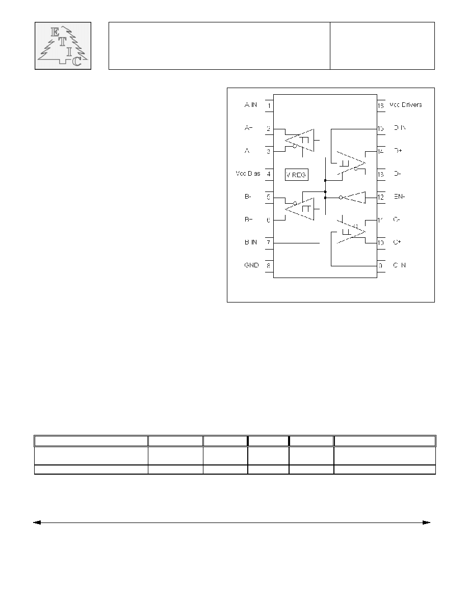
QUAD DIFFERENTIAL LINE DRIVER
WITH SEPARATE LOGIC BIAS AND DRIVER BIAS
SUPPLIES, AND ENABLE FUNCTION
ET7272
DESCRIPTION
These line drivers are pin compatible with 26LS31 in applications where pin 4 = 5V and pin 12 = GND. Internal clamp
diodes allow trouble-free operation when driving cable lengths exceeding 100m. Split supplies are provided to
minimize standby power dissipation in high voltage applications. The logic should be powered from a regulated 5V
supply at the VccBias pin. The output stages may then be powered by a separate supply at VccDrivers, up to 30V.
Output voltage swings of 0.3V to VCC-1.9V are typical. The outputs are protected against shorts to ground, shorts to
Vcc and to other outputs, by a two-fold scheme of current limiting and thermal shutdown. This assures highly reliable
operation in harsh environments. Heat-sinking may be accomplished at pin 8 which is directly connected to the ASIC
substrate.
APPLICATIONS
∑
Optical Encoders
∑
Industrial Controls
ABSOLUTE MAXIMUM RATINGS
Parameter
Symbol
Min.
Max.
Units
Ref.
Operating Temperature
Range
T
A
-55
115
∞C
Supply Voltage Range(both)
V
CC
4.5
30
V
ETIC
RESERVES THE RIGHT TO MAKE CHANGES AT ANY TIME TO IMPROVE THE DESIGN AND TO SUPPLY THE BEST PRODUCT.
©2000, Rev A1
iC-Haus GmbH
Tel +49-6135-9292-0
Integrated Circuits
Fax +49-6135-9292-192
Am Kuemmerling 18, D-55294 Bodenheim
http://www.ichaus.com
Page 2 of 3
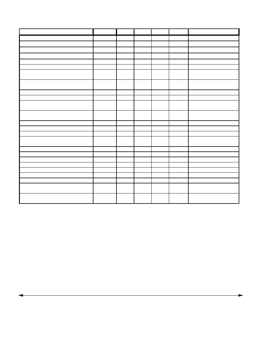
ELECTRICAL CHARACTERISTICS
Unless otherwise specified, T
A
= 25∞C and EN- <0.8V.
Parameters
Symbol
Min.
Typ.
Max.
Units
Test Conditions
Overtemp Operate Point (junction)
1
T
JOP
172
∞C
Overtemp Release Point (junction)
1
T
JRP
136
∞C
Vcc Bias Voltage Range
Vcc
B
3.5
5
30
V
Vcc Drivers Voltage Range
Vcc
D
4.5
5
30
V
Supply Current Vcc
B
1 (B
IAS
)
Icc
B
1
11.9
16.0
mA
Vcc
B
and Vcc
D
= 5V
Supply Current Vcc
D
1 (D
RIVERS
)
I
CCD
1
2.4
3.3
mA
Vcc
B
and Vcc
D
= 5V
Supply Current Vcc
B
2
Icc
B
2
2.5
3.4
mA
Vcc
B
and Vcc
D
= 5V,
EN- > 2V
Supply Current Vcc
D
2
I
CCD
2
0.0
0.1
mA
Vcc
B
and Vcc
D
= 5V,
EN- > 2V
Supply Current Vcc
B
3
Icc
B
3
12.1
18.5
mA
Vcc
B
and Vcc
D
= 30V
Supply Current Vcc
D
3
I
CCD
3
2.4
3.3
mA
Vcc
B
and Vcc
D
= 30V
Supply Current Vcc
B
4
Icc
B
4
2.6
3.5
mA
Vcc
B
and Vcc
D
= 5V,
EN- > 2V
Supply Current Vcc
D
4
I
CCD
4
0.0
0.1
mA
Vcc
B
and Vcc
D
= 5V,
EN- > 2V
Enable Input Threshold
V
THE
0.8
1.5
2
V
Enable Low Level Input Current
I
ILE
-10
0
10
µA
V
IN
= 0V, Vcc
B
= 5V
Enable High Level Input Current
I
IHE
-
108
150
µA
V
IN
= 5V, Vcc
B
= 5V
High Impedance Output Leakage
I
OZ
-4.0
0.0
4.0
µA
Vcc
D
=30V, EN- > 2V,
Output at 15V
Input Positive-Going Threshold
V
T
+
1.05
1.25
1.45
V
Vcc
B
= 5V
Input Negative-Going Threshold
V
T-
0.75
0.95
1.15
V
Vcc
B
= 5V
Input Hysteresis
V
H
-
0.3
-
V
Vcc
B
= 5V
Low Level Input Current
I
IL
-0.1
-4.0
µA
V
IN
= 0V, Vcc
B
= 5V
High Level Input Current
I
IH
0
4.0
µA
V
IN
= 5V, Vcc
B
= 5V
Low Level Output1
V
OL
1
375
500
mV
I
OL
= 20mA, Vcc
D
= 5V
Low Level Output2
V
OL
2
370
500
mV
I
OL
= 20mA, Vcc
D
=30V
High Level Output1
V
OH
1
2.4
2.8
V
I
OH
= -20mA, Vcc
D
=
5V
High Level Output2
V
OH
2
27.7
28.1
V
I
OH
= -20mA,
Vcc
D
=30V
ETIC
RESERVES THE RIGHT TO MAKE CHANGES AT ANY TIME TO IMPROVE THE DESIGN AND TO SUPPLY THE BEST PRODUCT.
©2000, Rev A1
iC-Haus GmbH
Tel +49-6135-9292-0
Integrated Circuits
Fax +49-6135-9292-192
Am Kuemmerling 18, D-55294 Bodenheim
http://www.ichaus.com
Page 3 of 3
AC SWITCHING CHARACTERISTICS
Values given at V
CC
B
= 5V, V
CC
D
= 24V, T
A
= 25∞C,
C
L
= 1000pF on all outputs, and EN- <0.8V.
Parameters
Symbol
Min.
Typ.
Max
.
Units
Test Conditions
Propagation delay, rising input 50%
point to zero crossing of differential
outputs
T
PLH
450
630
ns
Propagation delay, falling input 50%
point to zero crossing of differential
outputs
T
PHL
450
630
ns
Output Rise Time
T
R
700
980
ns
Output Fall Time
T
F
700
980
ns
NOTES:
1. This is not a test parameter, but for information
only.
2. It may be necessary to clamp the outputs with
Schottky diodes when driving extemely long
cables with high capacitance between outputs.
These diodes should have a forward voltage of
less than 0.4V, and be connected with cathode to
the output and anode to ground.
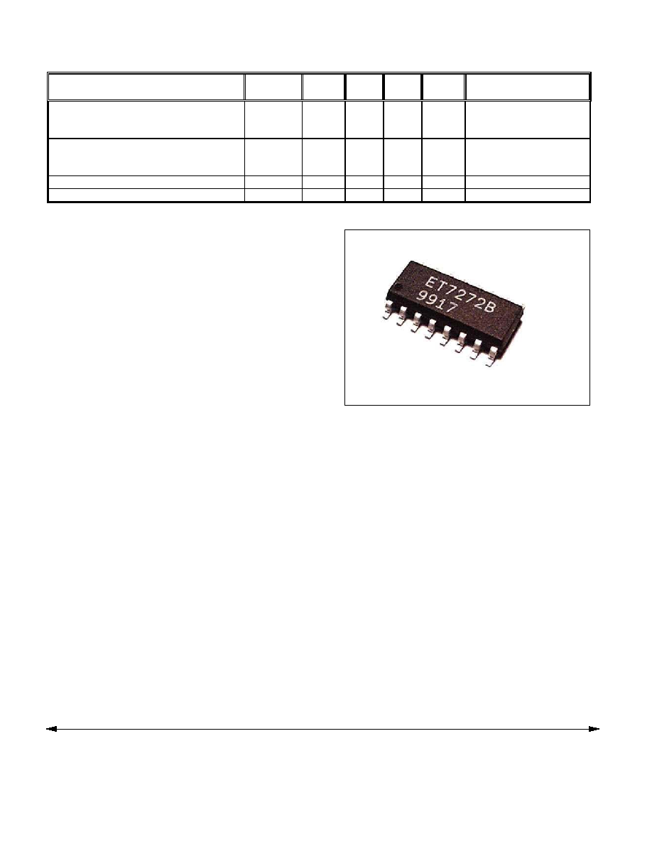
PACKAGE
SUFFIX
Chip Only
-C
16 Lead SOIC
-SOP