 | –≠–ª–µ–∫—Ç—Ä–æ–Ω–Ω—ã–π –∫–æ–º–ø–æ–Ω–µ–Ω—Ç: iC-NE-SO8 | –°–∫–∞—á–∞—Ç—å:  PDF PDF  ZIP ZIP |

iC-NE
LIGHT CHAIN PULSE RECEIVER
FEATURES
APPLICATIONS
Photoelectric amplifier adapted to standard photodiodes
Built-in bandpass filter with 300kHz center frequency
Differential current-signal output with open drain low-side
drivers
Nonlinear transfer function results in wide dynamic range of
100nA..600
µ
A for pulsed photocurrents
Fast flash recovery time of max. 30
µ
s
Recovery time below 10
µ
s for excessive photocurrents of up
to 1mA
3-step shift register and control logic
Compatible to CMOS levels
Single 5V supply
Low standby current; circuit activation by input data
Power-down reset
Small outline package SO8
Suited for high-risk applications according to IEC 1496-1
ESD protection
Option: extended temperature range of -20
∞
C to 85
∞
C
Light curtains
Light barriers
Electro-sensitive protective
equipment (ESPE)
PACKAGES
SO8
BLOCK DIAGRAM
©1999
Rev C0
OUTPUT STAGE
BP-AMPLIFIER
iC-NE
BIAS
LOGIC OUTPUT
POWER DOWN
RESET
1
CONTROL LOGIC
INPUTS
LOGIC
D
C
R
Q
Q3
FF3
D
C
R
Q
Q1
FF1
D
C
R
Q
Q2
FF2
SN
SP
EN
EN
PD
VDD
INH
GND
DOUT
DIN
CLK
+5V
8
2
5
4
6
µ
A
6
µ
A
Photo-
diode
7
3
6
1
BIAS
iC-Haus GmbH
Tel
+49-6135-9292-0
Integrierte Schaltkreise
Fax +49-6135-9292-192
Am Kuemmerling 18, 55294 Bodenheim
http://www.ichaus.com
iC-NE
LIGHT CHAIN PULSE RECEIVER
Rev C0, Page 2/9
DESCRIPTION
The iC-NE device is a light chain receiver IC. Typical applications cover light curtains, light barriers and
electro-sensitive protective equipment in general.
Integrated on a single silicon chip the iC-NE contains a bandpass amplifier with a center frequency of
typically 300kHz, a differential current-signal output stage plus control logic to activate the amplifier and the
output stage. In the deactivated state, the current consumption is very low and the current-signal outputs
SN and SP are switched to high impedance (zero current).
The logic consists of a three-stage shift register in which the first two stages are triggered by the rising
edge of the clock input CLK. The third flipflop is triggerred with the falling clock edge, what gives an
artificial delay in order to avoid race conditions when shifting the input data via the serial output to the next
device in the chain.
The bandpass amplifier is activated when DIN reads a logical '1'. The output stage still remains disabled
(zero current) until the output of the first flipflop changes to '1'. This turnes on the bias for the complete
signal path from light detection to the differential current-output stage. The differential outputs SN and SP
are powered up to an equal current niveau, as far as the attached photodiode does not receive any
changes in light.
The rising edge of a received light pulse (what means a negative going photocurrent step), causes the
output current at SN to decrease and at SP to increase by an equal value. The sum of I(SN)+I(SP) is kept
constant. For light curtain applications in which only one device is activated at a time, the outputs SN and
SP may be linked to a two-wire bus.
After processing the serial input data at DIN, the activated amplifier and output stage will return to standby
mode automatically, when the clock input gets the second rising edge. Therefore, a chain circuitry with
multiple beams has to be set up with just a single data bit within a shift cycle.
The IC contains protective diodes to prevent against destruction due to ESD. Logic input pins feature
Schmitt-trigger characteristics for high noise immunity. All pins are short-circuit proof.
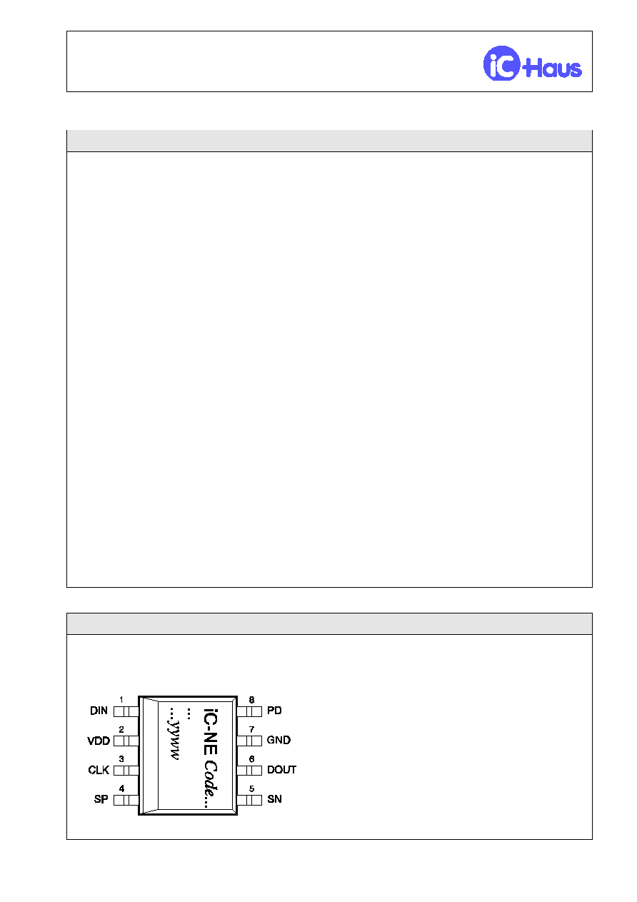
PACKAGE SO8 to JEDEC Standard
PIN CONFIGURATION SO8
PIN FUNCTIONS
(top view)
No. Name Function
1
DIN
Data Input
2
VDD
+5V Supply Voltage
3
CLK
Clock Input
4
SP
Pos. Differential current output
5
SN
Neg. Differential current output
6
DOUT Data Output
7
GND
Ground
8
PD
Photocurrent Input,
photodiode cathode

iC-NE
LIGHT CHAIN PULSE RECEIVER
Rev C0, Page 3/9
ABSOLUTE MAXIMUM RATINGS
Values beyond which damage may occur; device operation is not guaranteed.
Item
Symbol
Parameter
Conditions
Fig.
Unit
Min.
Max.
G001 VDD
Voltage at VDD
-0.5
7
V
G002 V()
Voltage at DIN, CLK, DOUT, SN, SP,
PD
-0.5
VDD+0.5
V
E001 Vd()
ESD Susceptibility at DIN, CLK,
DOUT, PD, SN, SP
MIL-STD-883, HBM
100pF discharged through 1.5k
2
kV
TG1 Tj
Junction Temperature
-40
150
∞
C
TG2 Ts
Storage Temperature
-40
150
∞
C
THERMAL DATA
Operating Conditions: VDD= 5V
±
10%
Item
Symbol
Parameter
Conditions
Fig.
Unit
Min.
Typ.
Max.
T1
Ta
Operating Ambient Temperature
Range
(extended temperature range
of -20..85
∞
C on request)
0
70
∞
C
All voltages are referenced to ground unless otherwise noted.
All currents into the device pins are positive; all currents out of the device pins are negative.

iC-NE
LIGHT CHAIN PULSE RECEIVER
Rev C0, Page 4/9
ELECTRICAL CHARACTERISTICS
Operating Conditions:
VDD= 5V
±
10%, V(SN,SP)= 3.5V..VDD, Tj= -20..85
∞
C, unless otherwise noted
Item
Symbol
Parameter
Conditions
Tj
Fig.
Unit
∞
C
Min.
Typ.
Max.
Total Device
001
VDD
Permissible Supply Voltage
Range
4.5
5.5
V
002
VDD
Required Supply Voltage for logic
function
decreasing voltage VDD
1.7
V
003
I(VDD)
Supply Current in VDD
(Standby)
DIN= lo, CLK= hi or lo:
BP-amplifier and output stage
disabled, logic levels:
lo= 0..0.45V,
hi= VDD-0.45V..VDD
60
µ
A
004
I(VDD)
Supply Current in VDD
EN= hi: BP-amplifier activated
INH= hi: output stage disabled,
I(PD)= -15..0
µ
A
27
0.3
0.5
mA
mA
005
I(VDD)
Supply Current in VDD
EN= hi, INH= lo: BP-amplifier and
output stage activated
27
1.1
3.0
mA
mA
006
VDDon
Turn-on Threshold VDD
(Power-on release)
4.0
V
007
VDDoff
Undervoltage Threshold at VDD
(Power-down reset)
decreasing voltage VDD
2.6
V
008
VDDhys
Hysteresis
VDDhys= VDDon-VDDoff
200
500
mV
009
Vc()hi
Clamp Voltage hi at DIN, CLK,
DOUT, PD, SN, SP
Vc()hi= V()-VDD,
I()= 10mA
0.4
1.25
V
010
Vc()lo
Clamp Voltage lo at DIN, CLK,
DOUT, PD, SN, SP
I()= -10mA, VDD= 0V
other pins open
-1.25
-0.4
V
Bandpass Amplifier and Output Stage PD, SN, SP
101
C(PD)
Permissible capacitance at PD
100
pF
102
V(PD)
Voltage at PD
0.9
V
103
I(PD)
Permissible DC-photocurrent in
PD (ambient light supression)
-15
0
µ
A
104
I(PD)mg
Monotone Gain Range of I(PD)pk differential output current
increases or remains constant
when I(PD)pk increases
3
-600
0
µ
A
105
twhi
Permissible Photocurrent Pulse
Duration
3
4
1.0
µ
s
106
twlo
Permissible Photocurrent Pause
Duration
2nd Gpk
90% 1st Gpk (resp. of
single pulse)
4
2.0
µ
s
107
trec
Flash Recovery Time
I(PD)pk= -1mA
10
µ
s
108
trec
Power-Flash Recovery Time
I(PD)pk= -5mA, magnitude of
photocurrent integral equal 15mA
30
µ
s
109
Gpk
Pulse Current Gain
Gpk= [Ipn()-IO*ISUM] / I(PD)pk;
I(PD)dc= -15..0
µ
A,
I(PD)pk= -1..-0.1
µ
A,
tr= tf= 0.5
µ
s, twpk= 1
µ
s
3
330
840
110
Gac
AC Current Gain
I(PD)dc= -15..-2.5
µ
A,
I(PD)ac= 5
µ
App sinussoidal
waveform, frequency for max.
gain
580
1070
111
fl
Lower Cut-off Frequency
(-3dB)
I(PD)dc= -15..-2.5
µ
A,
I(PD)ac= 5
µ
App sinussoidal
waveform
85
210
kHz

iC-NE
LIGHT CHAIN PULSE RECEIVER
Rev C0, Page 5/9
ELECTRICAL CHARACTERISTICS
Operating Conditions:
VDD= 5V
±
10%, V(SN,SP)= 3.5V..VDD, Tj= -20..85
∞
C, unless otherwise noted
Item
Symbol
Parameter
Conditions
Tj
Fig.
Unit
∞
C
Min.
Typ.
Max.
Bandpass Amplifier and Output Stage PD, SN, SP (continued)
112
fh
Upper Cut-off Frequency
(-3dB)
I(PD)dc= -15..-2.5
µ
A,
I(PD)ac= 5
µ
App sinussoidal
waveform
380
940
kHz
113
f
Bandwidth (-3dB)
f
= fh-fl
270
790
kHz
114
V(SN,SP) Permissible Voltage at SN, SP
3.5
VDD
V
115
ISUM
Output currents I(SN)+I(SP)
27
5.0
7.5
9.7
mA
mA
116
IO
Relative Offset Current
IO= [I(SN)-I(SP)] / ISUM; I(PD)= 0
-10
10
%
117
Ilk
Leakage Current I(SN)+I(SP)
output stage disabled
4.0
µ
A
118
Idlk()
Differential Leakage Current
Idlk()= I(SN)-I(SP);
I(PD)pk= -600
µ
A, twhi= 3
µ
s,
output stage disabled
3
-0.1
0.1
µ
A
119
Ipn()
Differential Output Current
Ipn()= I(SN)-I(SP);
I(PD)pk= -10
µ
A
3
-6.5
-3.0
mA
120
Ipn()
Differential Output Current
Ipn()= I(SN)-I(SP);
I(PD)pk= -100
µ
A
3
-11.0
-4.0
mA
121
INoise
Differential Output Current
Noise (RMS)
I(PD)dc= -15
µ
A, RGen= 500k
,
no additional filter
27
5
5
µ
A
122
INoise
Differential Output Current
Noise (RMS)
I(PD)dc= -15
µ
A, RGen= 500k
,
with BP-filter 50kHz-1.2MHz
27
5
3.5
µ
A
123
tp()IDCon Output Stage Turn-on Delay:
CLK lo
hi to 90% I(SN), I(SP)
I(PD)dc= -15
µ
A..0,
I(PD)ac= 0
4
3.0
µ
s
124
tp()IDCoff Output Stage Turn-off Delay:
CLK lo
hi to 10% I(SN), I(SP)
I(PD)dc= -15
µ
A..0,
I(PD)ac= 0
4
3.0
µ
s
Control Inputs DIN, CLK
201
Vt()hi
Threshold Voltage hi
66
%VDD
202
Vt()lo
Threshold Voltage lo
33
%VDD
203
Vhys()
Schmitt-Trigger Input Hysteresis
400
mV
204
Ipd()
Pull-Down Current
V()= 1V..VDD
27
3
6
12
µ
A
Output Buffer DOUT
301
Vs()hi
Saturation Voltage hi
Vs()hi= VDD-V(DOUT); I()= -4mA
0.4
V
302
Vs()lo
Saturation Voltage lo
I()= 4mA
0.4
V
303
Isc()hi
Short-Circuit Current hi
V()= 0V
27
-100
-50
-25
mA
mA
304
Isc()lo
Short-Circuit Current lo
V()= VDD
27
25
50
100
mA
mA
305
tr()
Rise Time
CL()= 50pF
27
20
60
ns
ns
306
tf()
Fall Time
CL()= 50pF
27
20
60
ns
ns
Switching Characteristics
401
tplh(CLK
-DOUT)
Propagation Delay:
CLK hi
lo until DOUT lo
hi
CL(DOUT)= 50pF
27
2
25
60
ns
ns
402
tphl(CLK
-DOUT)
Propagation Delay:
CLK hi
lo until DOUT hi
lo
CL(DOUT)= 50pF
27
2
25
60
ns
ns