 | –≠–ª–µ–∫—Ç—Ä–æ–Ω–Ω—ã–π –∫–æ–º–ø–æ–Ω–µ–Ω—Ç: iC-NG | –°–∫–∞—á–∞—Ç—å:  PDF PDF  ZIP ZIP |
iC-NG
8-BIT Sin/D CONVERTER-PROCESSOR
Rev C1, Page 1/21
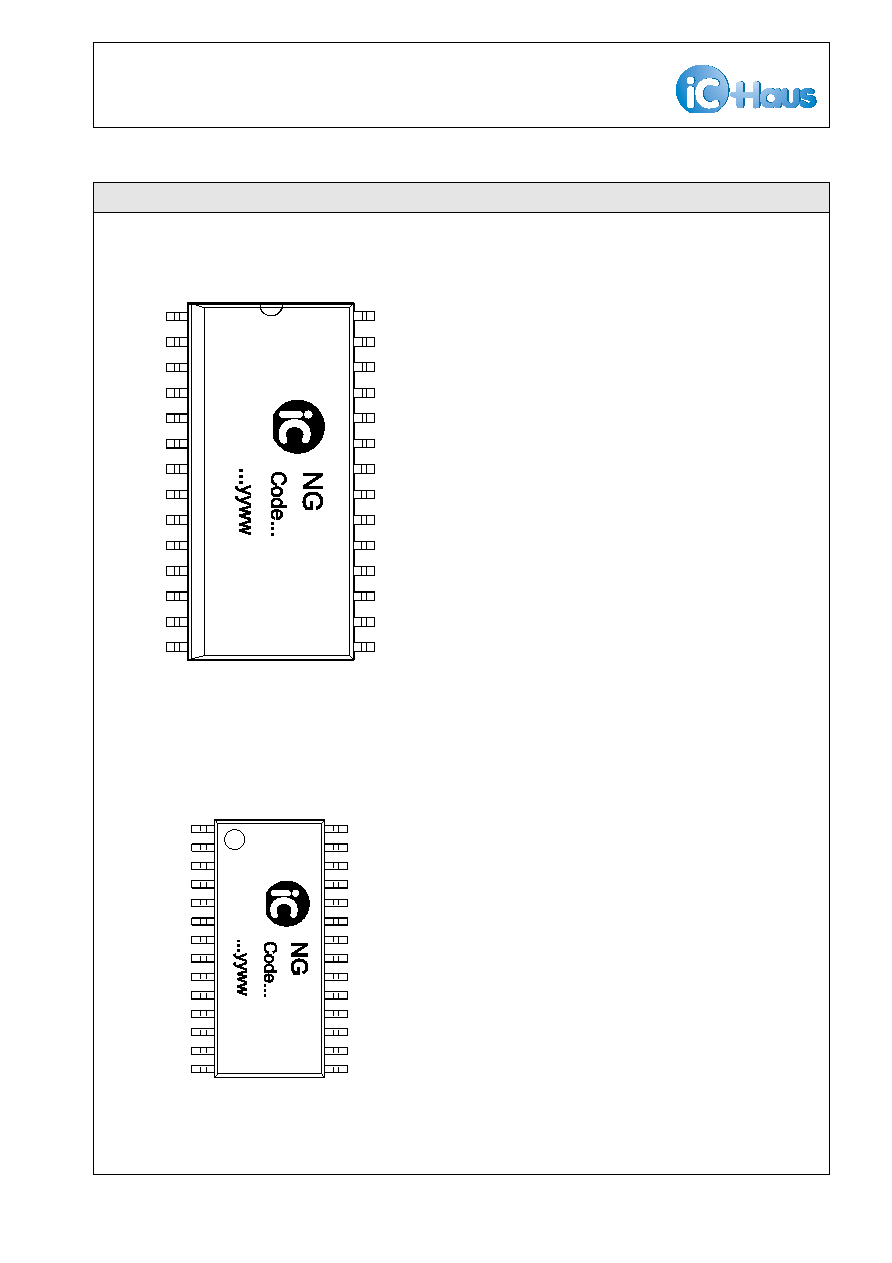
SO28
SSOP28
FEATURES
APPLICATIONS
∞
Real-time interpolator with a programmable resolution of up to
256 steps/period
∞
Calibration features permit adaptation of distorted sine/cosine
signals
∞
Output with A/B/Z incremental signals of up to 400kHz, as a
parallel 8-bit absolute vector or via a serial interface
∞
Error messaging with excessive input frequency
∞
Programmable index position
∞
Fast 24-bit multiturn counting (position capture with target
position interrupt)
∞
8-bit µP interface
∞
Interrupt controller
∞
Adjustable clock oscillator
∞
Front-end amplifiers configurable externally
∞
Chip setup can be loaded from a serial EEPROM
∞
TTL-compatible inputs, TTL-/CMOS-compatible outputs
∞
Inputs and outputs protected against destruction by ESD
∞
Absolute and incremental angle
interpolation from orthogonal
sinusoidal input signals
∞
Interpolating interface for MR
sensors and optical analog
encoders
PACKAGES
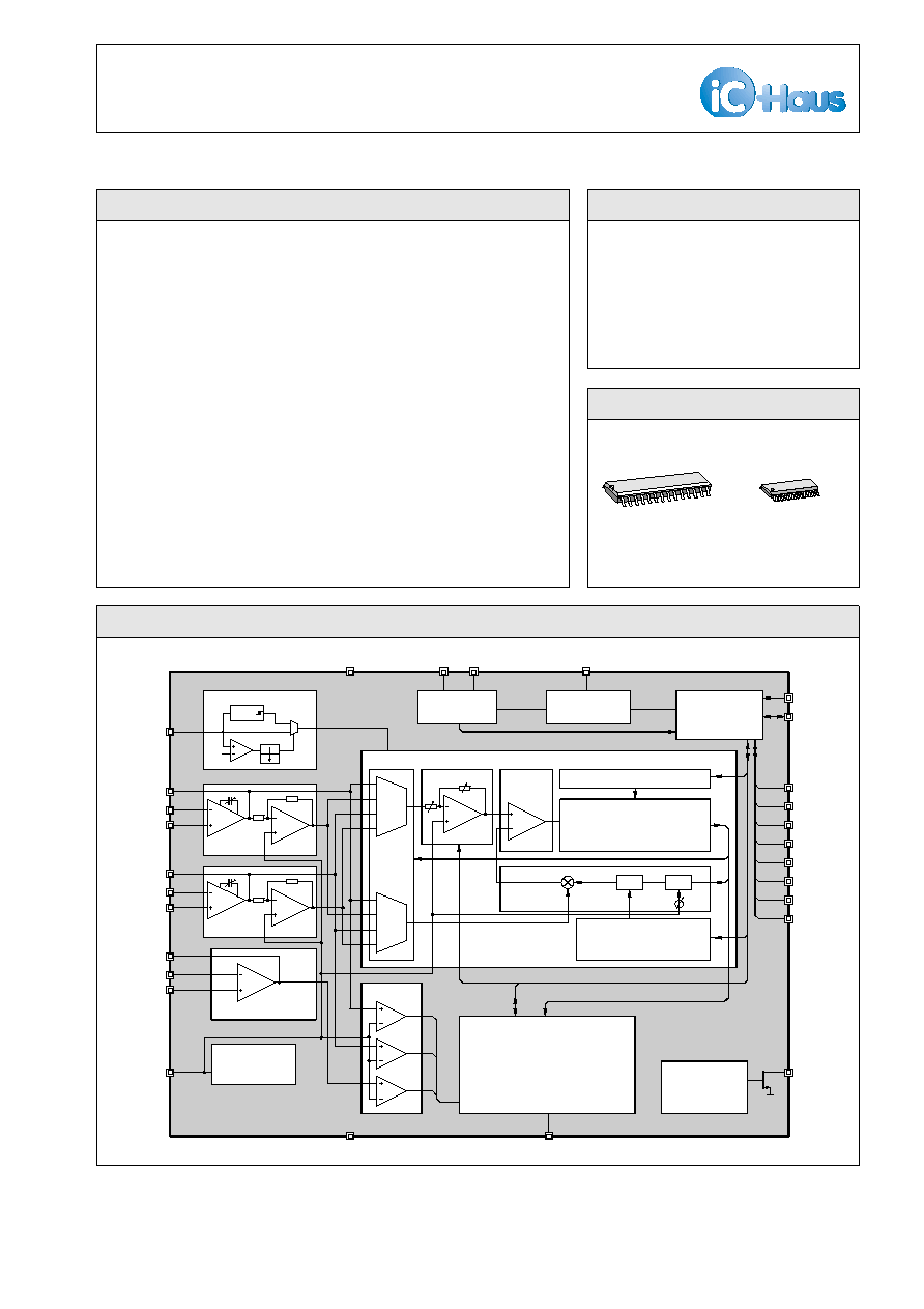
BLOCK DIAGRAM
© 2001
iC-Haus GmbH
Tel +49-6135-9292-0
Integrated Circuits
Fax +49-6135-9292-192
Am Kuemmerling 18, D-55294 Bodenheim
http://www.ichaus.com
COS
21
D0
5
D1
6
D2
7
D3
8
D4
9
D5
10
D6
11
25
MFP
2
NCOS
20
NER
1
NRD
3
NRES
26
NSIN
23
NWR
4
NZERO
17
PCOS
19
PSIN
22
PZERO
16
RCLK
13
SCL
28
SDA
27
SIN
24
VDD
14
VREF
15
ZERO
18
D7
12
GND
DIGITAL SIGNAL PROCESSING
24-Bit Counter
Interrupt Controller
RPM/Speed Aquisition
Index/Zero Pulse Justification
Incremental Signal Generator
Mode Switch (Frequency Overrun)
Resolution, Hysteresis
iC-NG
µP INTERFACE
SERIAL EEPROM
INTERFACE
ERROR MONITOR
(per segment)
Converter Function Adaptation
TAN D/A
D/A
tan
A ◊ sin
tan(phi)
phi
phi
Up/Down Counter
Binary
SINE / DIGITAL CONVERTER
PGA
A ◊ sin
MUX
Segment
A ◊ cos
Z4
A4
B4
CLK INPUT/OSCILLATOR
INPUT INDEX/ZERO
INPUT COS
INPUT SIN
Comparator
2V
R/f
internal data bus
4-FOLD EDGE
EVALUATION
STATE CONTROL
REFERENCE
VOLTAGE
Converter
OFFS
2.4V

iC-NG
8-BIT Sin/D CONVERTER-PROCESSOR
Rev C1, Page 2/21
DESCRIPTION
iC-NG is a monolithic A/D converter which determines
the angle value of two sinusoidal input signals phase-
shifted at 90∞ with a given resolution and hysteresis. In
this process a cycle is divided into 8 segments; each
of these segments can be given a resolution of up to
32 angular steps. Resolutions of 1 to 256 divisions per
cycle are possible.
The converter can be adjusted for each individual seg-
ment to suit various types of input signal, meaning that
even distorted sine signals or triangular signals, for
example, can be converted. In addition, the direction
of rotation can be inverted and the zero position can
be set in steps of 45∞.
Output values and parameters are stored in registers
connected to the internal 8-bit data bus. A parallel
microcontroller interface gives read and write access
to these registers. If an EEPROM is connected to the
serial interface, the chip setup can be automatically
read in following a reset.
The output value consists of an 8-bit word for interpo-
lation within a cycle and a 24-bit position counter
which logs the number of turns. In addition to normal
accessibility, the output value can also be transferred
serially.
The position counter can be reset via the zero pulse or
stopped and started using the bi-directional MFP pin.
When programmed as an output, pin MFP shows the
change in output value or indicates when a certain
position has been reached (interrupt output). After a
reset, the interpolation result is correct after just a few
clock cycles, even with static input signals.
If incremental mode is selected, the changes in angle
are output as square-wave signals phase-shifted at
90∞ at pins D0(AX) and D1(BX) with a selected resolu-
tion and at pins D3(A4) and D4(B4) with a resolution of
four. The suitably prepared zero signal is at D2(ZX)
and D5(Z4). Pin D6(ROT) shows the direction of rota-
tion. Tracks AX and BX are EX-OR-gated at pin
D7(AXB).
The front-end amplifier connections are all lead out,
enabling current or voltage inputs to be made. Com-
plementary input signals can also be connected. The
front-end amplifiers are compensated internally; the
value of compensation can be programmed.
The internal clock frequency can be adjusted using an
external resistor or can be fed in via pin RCLK. The
clock pulses which occur between two changes in
output are counted in order to calculate the number of
revolutions. Low voltage and excessive input fre-
quency errors are signaled at output NER (open
drain). These error codes are stored in the relevant
register.
iC-NG
8-BIT Sin/D CONVERTER-PROCESSOR
Rev C1, Page 3/21
7
D4
D5
D6
D7
VDD
D3
D2
8
9
10
11
12
13
14
NCOS
PCOS
NZERO
PZERO
VREF
COS
22
21
20
19
18
17
16
15
1
NRD
NWR
D0
D1
MFP
NER
2
3
4
5
6
NRES
GND
SIN
NSIN
SDA
SCL
28
27
26
25
24
23
RCLK
ZERO
PSIN
1
2
3
4
5
6
7
8
9
10
24
23
22
21
20
19
28
27
26
25
11
12
13
14
18
17
16
15
D4
D5
D6
D7
VDD
D3
D2
NCOS
PCOS
NZERO
PZERO
VREF
COS
NRD
NWR
D0
D1
MFP
NER
NRES
GND
SIN
NSIN
SDA
SCL
RCLK
ZERO
PSIN
PACKAGE SO28, SSOP28 to JEDEC Standard
PIN CONFIGURATION SO28
PIN FUNCTIONS
(top view)
No.
Name
Function
1
NER
Error Message Output, low active
2
MFP
Multi-Functional I/O Pin
3
NRD
Read Signal, low active
1)
/ SSI Clock
4
NWR
Write Signal, low active
1)
/ SSI Output
5
D0
Data Bus / Incremental Output A (AX)
6
D1
Data Bus / Incremental Output B (BX)
7
D2
Data Bus / Index Output Z (ZX)
8
D3
Data Bus / Sine-to-Square Output A (A4)
9
D4
Data Bus / Cosine-to-Square Output B (B4)
10
D5
Data Bus / Index-to-Square Output Z (Z4)
11
D6
Data Bus / CW-CCW Signal (ROT)
12
D7
Data Bus / AX EXOR BX (AXB)
13
RCLK
Clock Input / Clock Oscillator Setting
14
VDD
+5V Supply Voltage
15
VREF
Reference Center Voltage
16
PZERO
Zero Amplifier Positive Input
17
NZERO
Zero Amplifier Negative Input
18
ZERO
Zero Amplifier Output
19
PCOS
Cosine Amplifier Positive Input
20
NCOS
Cosine Amplifier Negative Input
21
COS
Cosine Amplifier Output
22
PSIN
Sine Amplifier Positive Input
23
NSIN
Sine Amplifier Negative Input
24
SIN
Sine Amplifier Output
25
GND
Ground
26
NRES
Reset, low active
27
SDA
Mode Select / Data (Serial Interface)
28
SCL
Mode Select / Clock (Serial Interface)
Notes: 1) wiring to VDD recommended when not in use.
PIN CONFIGURATION SSOP28 5.3mm
(top view)
iC-NG
8-BIT Sin/D CONVERTER-PROCESSOR
Rev C1, Page 4/21
All voltages are referenced to ground unless otherwise noted.
All currents into the device pins are positive; all currents out of the device pins are negative.
ABSOLUTE MAXIMUM RATINGS
Values beyond which damage may occur; device operation is not guaranteed.
Item
Symbol
Parameter
Conditions
Fig.
Unit
Min.
Max.
G001 VDD
Supply Voltage
-0.3
6.0
V
G002 V()
Voltage at
SIN, NSIN, PSIN, COS, NCOS, PCOS,
ZERO, NZERO, PZERO, VREF, MFP,
RCLK, NER, D0..7, NRD, NWR,
NRES, SCL, SDA
-0.3
VDD+0.3
V
G003 Imx(VDD) Current in VDD
-50
50
mA
G004 Imx(GND) Current in GND
-50
50
mA
G005 Ic()
Current in Clamping Diodes SIN,
NSIN, PSIN, COS, NCOS, PCOS, ZE-
RO, NZERO, PZERO, VREF, MFP,
RCLK, NER, D0..7, NRD, NWR,
NRES, SCL, SDA
MFP, D0..7, NWR
with input function
-5
5
mA
G006 I()
Current in SIN, COS, ZERO, VREF,
MFP, NER, D0..7, NWR, SCL
MFP, D0..7, NWR
with output function
-10
10
mA
G007 Ilu()
Pulse Current in all Pins
(Latch-Up Strength)
pulse duration
#
10µs
-100
100
mA
E001 Vd()
ESD Susceptibility at all Pins
MIL-STD-883, Method 3015, HBM;
100pf discharged through 1.5k
S
2
kV
TG1 Tj
Junction Temperature
-40
150
∞C
TG2 Ts
Storage Temperature
-40
150
∞C
THERMAL DATA
Operating conditions: VDD= 5V ±10%
Item
Symbol
Parameter
Conditions
Fig.
Unit
Min.
Typ.
Max.
T1
Ta
Operating Ambient Temperature Range
(extended temperature range on
request)
-20
70
∞C
iC-NG
8-BIT Sin/D CONVERTER-PROCESSOR
Rev C1, Page 5/21
ELECTRICAL CHARACTERISTICS
Operating conditions: VDD= 5V ±10%, Tj= -40..125∞C, unless otherwise noted.
Item
Symbol
Parameter
Conditions
Tj
Fig.
Unit
∞C
Min.
Typ.
Max.
Total Device
001
VDD
Permissible Supply Voltage
4.5
5.5
V
002
I(VDD)
Supply Current
outputs not active
5
25
mA
003
Vt()hi
Input Threshold Voltage hi at
D0..D7, MFP,NRD,NWR,NRES
2
V
004
Vt()lo
Input Threshold Voltage lo at
D0..D7, MFP,NRD,NWR,NRES
0.8
V
005
Vt()hys
Input Hysteresis at
D0..D7, MFP,NRD,NWR,NRES
Vt()hys= Vt()hi -Vt()lo
300
mV
006
Iin()
Input Current at
D0..D7, MFP,NRD,NWR,NRES
-1
+1
µA
007
Vs()lo
Saturation Voltage lo at
D0..D7, MFP
I()= 4mA
0.4
V
008
Vs()hi
Saturation Voltage hi at
D0..D7, MFP
Vs()hi= VDD -V();
I()= -4mA
0.4
V
E001 Vc()hi
Clamp Voltage hi at all Pins
Vc()hi= V() -VDD;
I()= 5mA, other pins open
0.3
1.5
V
E002 Vc()lo
Clamp Voltage lo at all Pins
I()= 5mA, other pins open
-1.5
-0.3
V
Input Amplifiers SIN, COS, INDEX/ZERO
101
Vin()
Recommended Input Voltage
Range
1
3.5
Vpp
102
Vos()
Input Offset Voltage
Vin()= 1V..VDD -1V
-10
+10
mV
103
Iin()
Input Current
-50
+50
nA
104
Vcm()
Common Mode Voltage Range
Iout()= 0..±5mA
0.1
VDD-
1.0
V
105
Vs()hi
Saturation Voltage hi
Vs()hi= VDD -V(), Iout()= -5mA
0.5
V
106
Vs()lo
Saturation Voltage lo
Iout()= 5mA
0.5
V
107
SR0
Slew-Rate
CL= 0, C
C
= 0 (C
C
programmed)
4
V/µs
108
SR1
Slew-Rate
CL= 300pF, C
C
= 4pF
2
V/µs
109
SR2
Slew-Rate
CL= 800pF, C
C
= 6.4pF
1.2
V/µs
110
SR3
Slew-Rate
CL= 1.5nF, C
C
= 12pF
0.8
V/µs
111
GBW0
Gain Bandwidth Product
CL= 0, C
C
= 0 (C
C
programmed)
4.1
MHz
112
GBW1
Gain Bandwidth Product
CL= 300pF, C
C
= 4pF
1
MHz
113
GBW2
Gain Bandwidth Product
CL= 800pF, C
C
= 6.4pF
0.75
MHz
114
GBW3
Gain Bandwidth Product
CL= 1.5nF, C
C
= 12pF
0.4
MHz
Reference VREF
115
V(VREF) Reference Voltage
I(VREF)= 0..-1mA
2.2
2.4
2.6
V
Error Monitor NER
201
Vs()lo
Saturation Voltage lo at NER
I(NER)= 5mA
0.2
0.7
V
202
Isc()lo
Short-Circuit Current lo in NER
V(NER)= 0.4..VDD+0.3V
5
21
mA
203
I0()
Leakage Current in NER
V(NER)= 0..VDD+0.3V,
NER= hi oder VDD< 0.3V
10
µA
204
VDDon
Turn-on Threshold VDD
4.7
V
205
VDDoff
Undervoltage Threshold VDD
decreasing voltage VDD
4.5
V
206
VDDhys
Hysteresis
VDDhys= VDDon -VDDoff
200
mV
207
VDDerr
Supply Voltage VDD for Monitor
Operation
2.2
5.5
V