iC-VX
3-CHANNEL DIFFERENTIAL LINE DRIVER
Rev C1, Page 1/11
SO16W
TSSOP20
thermal pad
FEATURES
APPLICATIONS
∞
6 current-limited and short-circuit-proof push-pull driver
stages in complementary configuration
∞
Guaranteed driver current can be set to 30mA or 100mA
∞
Outputs compatible to TTL at low load current
∞
Integrated free-wheeling diodes
∞
Short switching times and high slew rate
∞
Schmitt trigger inputs with integrated pull-up current sources
and clamping diodes
∞
Inputs compatible to TTL and CMOS levels
∞
Operating points can be shifted by separate feed of inputs
∞
On-chip thermal shutdown with hysteresis
∞
Extended temperature range of -25..85
E
C
∞
Line driver for 24V control
engineering
PACKAGES
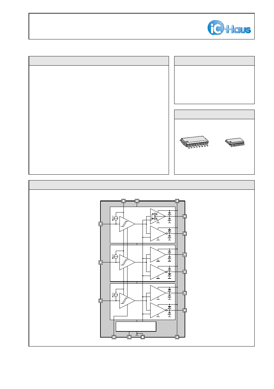
BLOCK DIAGRAM
© 2001
iC-Haus GmbH
Tel +49-6135-9292-0
Integrated Circuits
Fax +49-6135-9292-192
Am Kuemmerling 18, D-55294 Bodenheim
http://www.ichaus.com
CHAN1
CHAN2
CHAN3
THERMAL SHUTDOWN
BIAS
VSUB
12
E2
2
E1
1
E3
7
PROG
5
VEE
4
VB2
8
NA1
14
A1
15
A2
13
NA2
11
A3
10
NA3
9
VB1
16
VT
6
VCC
3
iC-VX
SO16W
iC-VX
3-CHANNEL DIFFERENTIAL LINE DRIVER
Rev C1, Page 2/11
1
n.c.
2
E1
3
E2
4
VCC
5
VEE
6
PROG
7
VT
8
E3
9
VB2
10
n.c.
n.c.
20
A1
19
NA1
18
A2
17
16
VSUB
15
NA2
14
A3
13
NA3
12
n.c.
11
VB
DESCRIPTION
The device iC-VX is a monolithic, 3-channel line driver with complementary outputs for 24V applications.
The Schmitt trigger inputs contain pull-up current sources and run on separate operating voltages. Their
reference potential can be adjusted in the range of the output stage supply voltage to adapt the input threshold
voltage for various applications.
The guaranteed driver current can be set to 30mA (PROG pin open) or 100mA (PROG pin at VSUB). At low
load the drivers are TTL-compatible due to reduced saturation voltages. The output stages are current-limited
and, due to the shutdown at overtemperature, they are also protected against thermal destruction. Due to the
hysteresis of the overtemperature shutdown, the driver outputs switch on and off as a function of the iC power
loss until the overload ceases.
For 30mA driver current the short-circuit strength is guaranteed directly by the iC. For 100mA driver current
in 24V applications this is guaranteed by 30
S
series resistors.
Free-wheeling diodes at the outputs protect the iC against echoes of mismatched lines. The inputs and
outputs of the channels have diodes for protection against destruction by ESD.
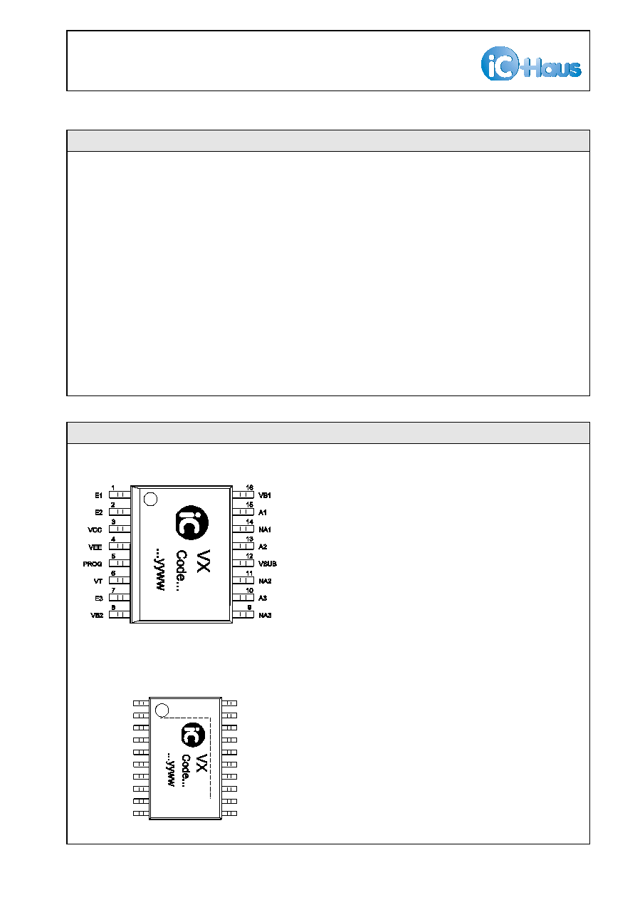
PACKAGES SO16W, TSSOP20 to JEDEC Standard
PIN CONFIGURATION SO16W
PIN FUNCTIONS
(top view)
Name
Function
E1
Input Channel 1
E2
Input Channel 2
VCC
Inputs Supply Voltage (+5V)
VEE
Reference Voltage for Inputs (0V)
PROG
Programming Input for Driver Current
(open 30mA, PROG to VSUB 100mA)
VT
+4.5..+30V Bias Supply Voltage
E3
Input Channel 3
VB2
+4.5..+30V Drivers Supply Voltage
NA3
Inverting Output Channel 3
A3
Output Channel 3
NA2
Inverting Output Channel 2
VSUB
Ground, Substrate
PIN CONFIGURATION TSSOP20tp 4.4mm
A2
Output Channel 2
(top view)
NA1
Inverting Output Channel 1
A1
Output Channel 1
VB1
+4.5..+30V Drivers Supply Voltage
Pins VB1 and VB2 must both be connected when
the 100mA driver current is set.
To enhance heat removal, the TSSOP20 package
offers a large area pad to be soldered (a connection
is only permitted to VSUB).

iC-VX
3-CHANNEL DIFFERENTIAL LINE DRIVER
Rev C1, Page 3/11
All voltages are referenced to ground unless otherwise noted.
All currents into the device pins are positive; all currents out of the device pins are negative.
ABSOLUTE MAXIMUM RATINGS
Values beyond which damage may occur; device operation is not guaranteed.
Item
Symbol
Parameter
Conditions
Fig.
Unit
Min.
Max.
G001 VCC-VEE Supply Voltage for Schmitt Trigger
Inputs
0
12
V
G002 VB1, VB2 Positive Supply Voltage for
Output Drivers
0
32
V
G003 VT
Bias Supply Voltage
0
30
V
G004 V(PROG) Voltage at PROG
0
2
V
G005 I(A,NA)
Output Current in A1..3, NA1..3
-300
300
mA
G006 I(E)
Current in E1..3
-8
8
mA
E001 Vd()
ESD Susceptibility, all Inputs and
Outputs
MIL-STD-883, Method 3015, HBM
100pF discharged through 1.5k
S
1
kV
TG1 Tj
Junction Temperature
-40
155
∞C
TG2 Ts
Storage Temperature
-40
150
∞C
THERMAL DATA
Operating Conditions: VB= 4.5..30V, VT= VCC= 5V ±10%
Item
Symbol
Parameter
Conditions
Fig.
Unit
Min.
Typ.
Max.
T1
Ta
Operating Ambient Temperature
Range
(extended range to -40∞C on request)
-25
85
∞C
T2
Rthja
SO16W Thermal Resistance
Junction to Ambient
surface mounted with ca. 2cm≤
heat sink at leads (see Demo Board)
55
75
K/W
T3
Rthja
TSSOP20 Thermal Resistance
Junction to Ambient
surface mounted, thermal pad
soldered to ca. 2cm≤ heat sink
30
40
K/W

iC-VX
3-CHANNEL DIFFERENTIAL LINE DRIVER
Rev C1, Page 4/11
ELECTRICAL CHARACTERISTICS
Operating Conditions:
VEE= VSUB= 0V, VB= 4.5..30V, VT= VCC= 5V ±10%, Tj= -25..125∞C, unless otherwise noted
Item
Symbol
Parameter
Conditions
Tj
Fig.
Unit
∞C
Min.
Typ.
Max.
Total Device
001
VCC-
VEE
Permissible Supply Voltage
Range for Inputs
4.5
11
V
002
VCC
Permis. Supply Voltage VCC
4.5
VB
V
003
VEE
Permis. Supply Voltage VEE
0
VB
-4.5V
V
004
I(VCC)
Supply Current in VCC
27
125
0.5
1.35
0.89
2.4
mA
mA
mA
005
VT
Permis. Bias Supply Voltage VT
4.5
VB
V
006
I(VT)
Supply Current in VT
PROG at VSUB
27
125
3
6.4
5.1
12
mA
mA
mA
007
I(VT)
Supply Current in VT
PROG open
27
125
1.3
2.6
2.2
5
mA
mA
mA
008
VB1,
VB2
Permis. Drivers Supply Voltage
at VB1 and VB2
4.5
30
V
009
I(VB)
Supply Current in VB
PROG at VSUB,
I(A1..3, NA1..3)= 0
27
125
0.6
2.1
1.5
4.8
mA
mA
mA
010
I(VB)
Supply Current in VB
PROG open,
I(A1..3, NA1..3)= 0
27
125
0.15
0.42
0.31
1.2
mA
mA
mA
Driver Outputs A1..3, NA1..3
101
Vs()hi
Saturation Voltage hi
(driver capability 100mA)
PROG to VSUB, VB1 and VB2
connected,
Vs(A)hi= VB-V(A,NA);
I(A,NA)= -10mA
I(A,NA)= -30mA
I(A,NA)= -100mA
1.0
1.2
2.0
V
V
V
102
Vs()lo
Saturation Voltage lo
(driver capability 100mA)
PROG to VSUB, VB1 and VB2
connected;
I(A,NA)= 10mA
I(A,NA)= 30mA
I(A,NA)= 100mA
0.9
1.0
1.5
V
V
V
103
Isc()hi
Short-Circuit Current hi
(driver capability 100mA)
PROG to VSUB, VB1 and
VB2 connected, V(A,NA)= 0V
-350
-100
mA
104
Isc()lo
Short-Circuit Current lo
(driver capability 100mA)
PROG to VSUB, VB1 and
VB2 connected, V(A,NA)= VB
100
350
mA
105
Ë
SR()
Ë
Slew-Rate hi
:
lo
(driver capability 100mA)
PROG to VSUB, VB1 and VB2
connected,
RL(A,NA)= 750
S
,
CL(A,NA)= 100pF
100
V/µs

iC-VX
3-CHANNEL DIFFERENTIAL LINE DRIVER
Rev C1, Page 5/11
ELECTRICAL CHARACTERISTICS
Operating Conditions:
VEE= VSUB= 0V, VB= 4.5..30V, VT= VCC= 5V ±10%, Tj= -25..125∞C, unless otherwise noted
Item
Symbol
Parameter
Conditions
Tj
Fig.
Unit
∞C
Min.
Typ.
Max.
Driver Outputs A1..3, NA1..3 (continued)
106
Vs()hi
Saturation Voltage hi
(driver capability 30mA)
PROG open, Vs()hi= VB-V(A,NA);
I(A,NA)= -3mA
I(A,NA)= -10mA
I(A,NA)= -30mA
0.9
1.0
1.4
V
V
V
107
Vs()lo
Saturation Voltage lo
(driver capability 30mA)
PROG open;
I(A,NA)= 3mA
I(A,NA)= 10mA
I(A,NA)= 25mA, VB= 4.5..10V
I(A,NA)= 30mA, VB= 10..30V
0.9
1.0
1.2
1.2
V
V
V
V
108
Isc()hi
Short-Circuit Current hi
(driver capability 30mA)
PROG open, V(A,NA)= 0V
-100
-30
mA
109
Isc()lo
Short-Circuit Current lo
(driver capability 30mA)
PROG open, V(A,NA)= VB
30
100
mA
110
Ë
SR()
Ë
Slew-Rate hi
:
lo
(driver capability 30mA)
PROG open, RL(A/NA)= 750
S
,
CL(A/NA)= 100pF
30
V/µs
111
Vs()lo
Saturation Voltage lo
for TTL-Levels
I(A,NA)= 1.6mA
0.4
V
112
I0(A,NA)
Tri-state Leakage Current
Tj> Toff, V(A,NA)= 0..VB
-100
100
µA
113
Vc()hi
Clamp Voltage hi
Vc(A,NA)hi= V(A)-VB;
I(A,NA)= 100mA
0.4
1.7
V
114
Vc()lo
Clamp Voltage lo
I(A,NA)= -100mA
-1.7
-0.4
V
Inputs E1..3
201
Vt(E)hi
Threshold Voltage hi
referred to VCC-VEE
45
%
202
Vt(E)lo
Threshold Voltage lo
referred to VCC-VEE
35
%
203
Vt(E)hys
Hysteresis
3
6
%
204
I(E)
Input Current
V(E)= VEE..VCC-1V
-81
-55
-30
µA
205
Vc(E)hi
Clamp Voltage hi
Vc(E)hi= V(E)-VCC; I(E)= 4mA
0.4
1.6
V
206
Vc(E)lo
Clamp Voltage lo
I(E)= -4mA
-1.6
-0.4
V
207
tp()
Propagation Delay E
6
A, E
6
NA
(driver capability 100mA)
50%V(E) : 50%I(A,NA);
PROG to VSUB, RL(A/NA)= 750
S
0.4
1
µs
208
)
tp
(A-NA)
Delay Skew A vs. NA
(driver capability 100mA)
)
tp()=
Ë
tp(E-A) -tp(E-NA)
Ë
;
PROG to VSUB, RL(A/NA)= 750
S
0.15
0.5
µs
209
tp()
Propagation Delay E
6
A, E
6
NA
(driver capability 30mA)
50%V(E) : 50%I(A,NA);
PROG open, RL(A/NA)= 750
S
0.8
2
µs
210
)
tp
(A-NA)
Delay Skew A vs. NA
(driver capability 30mA)
)
tp()=
Ë
tp(E-A) -tp(E-NA)
Ë
;
PROG open, RL(A/NA)= 750
S
0.35
1
µs
Thermal Shutdown, Bias
301
Toff
Thermal Shutdown Threshold
125
135
155
∞C
303
Thys
Thermal Shutdown Hysteresis
15
22
30
∞C