 | –≠–ª–µ–∫—Ç—Ä–æ–Ω–Ω—ã–π –∫–æ–º–ø–æ–Ω–µ–Ω—Ç: iC-WJZ | –°–∫–∞—á–∞—Ç—å:  PDF PDF  ZIP ZIP |
iC-WJ, iC-WJZ
LASER DIODE DRIVER
FEATURES
APPLICATIONS
Laser diode driver for continuous and intermittent operation
(CW to 300kHz) up to 250mA
Averaging control of laser power
Simple adjustment of the laser power via external resistor
Adjustable watchdog at the switching input to protect the
laser diode
Smooth starting after power-on
Driver shutdown in the case of overtemperature and
undervoltage
Single 5V supply
Simple circuitry
iC-WJ for laser diodes with 50..500
µ
A monitor current
iC-WJZ for laser diodes with 0.15..1.5mA monitor current
Driver with protective functions
for CW laser diodes
PACKAGES
iC-WJ, iC-WJZ
SO8
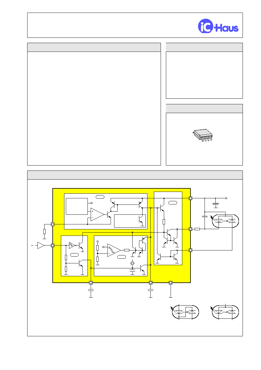
BLOCK DIAGRAM
©1997
Rev A1
+5V
100
µ
F
C1
DRIVER STAGE
INPUT
POWER DOWN
THERMAL
WATCHDOG
REFERENCE
REF
VCC
REF
1
2
3
4
100nF..470nF
CI
CWD
RSET
10k
74HCxx
KLD
VCC
CI
CWD
IN
GND
ISET
AMD
usable LD models
MD
LD
SHUTDOWN
iC-WJ/WJZ
1:1 iC-WJ
1:3 iC-WJZ
R1
12
C3
2nF
5
8
7
1
3
2
6
4
iC-Haus GmbH
Tel
+49-6135-9292-0
Integrated Circuits
Fax +49-6135-9292-192
Am Kuemmerling 18, D-55294 Bodenheim
http://www.ichaus.com
iC-WJ, iC-WJZ
LASER DIODE DRIVER
Rev A1, Page 2/12
DESCRIPTION
The iC-WJ and iC-WJZ devices are driver ICs for laser diodes in continuous and intermittent operation up
to 300kHz. The laser diode is activated via switching input IN. A control to the mean value of the optical
laser power and integrated protective functions ensure nondestructive operation of the sensitive
semiconductor laser.
The IC contains protective diodes to prevent destruction due to ESD, a protective circuit to guard against
overtemperature and undervoltage and a starting circuit for the laser diode driver to protect the laser diode
when switching on the supply voltage.
An external resistor at ISET is employed to adapt the power control to the laser diode being used. The
capacitor at CI determines the recovery time constants and the starting time.
A watchdog circuit monitors the switching input IN. If IN remains low longer than preset by the capa-citor at
CWD, the capacitor of the power control is discharged at pin CI. This ensures that the current through the
laser diode during the next high pulse at input IN is not impermissibly high.
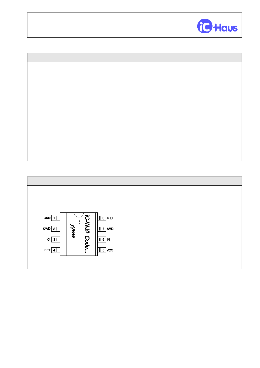
PACKAGES SO8 to JEDEC Standard
PIN CONFIGURATION SO8
PIN-FUNKTIONEN
(top view)
No. Name Function
1
GND
Ground
2
CWD
Capacitor for Watchdog
3
CI
Capacitor for Power Control
4
ISET
Attachment for RSET
5
VCC
5V Supply Voltage
6
IN
Input
7
AMD
Anode Monitor Diode
8
KLD
Cathode Laser Diode

iC-WJ, iC-WJZ
LASER DIODE DRIVER
Rev A1, Page 3/12
ABSOLUTE MAXIMUM RATINGS
Values beyond which damage may occur; device operation is not guaranteed.
Item
Symbol
Parameter
Conditions
Fig.
Unit
Min.
Max.
G001 VCC
Supply Voltage
0
6
V
G101 I(CI)
Current in CI
-4
4
mA
G102 V(KLD)
Voltage at KLD
IN= lo
0
6
V
G103 I(KLD)
Current in KLD
IN= hi
-4
600
mA
G104 I(AMD)
Current in AMD
-4
4
mA
G201 I(IN)
Current in IN
-10
2
mA
G301 I(ISET)
Current in ISET
-2
2
mA
G401 I(CWD)
Current in CWD
IN= lo
-2
2
mA
EG1 Vd()
ESD Susceptibility at
CWD, CI, ISET, IN, AMD, KLD
MIL-STD-883, HBM 100pF
discharged through 1.5k
2
kV
TG1 Tj
Junction Temperature
-40
150
∞
C
TG2 Ts
Storage Temperature
-40
150
∞
C
iC-WJZ with a monitor current rating of 0.15..1.5mA
Max. ratings for iC-WJ are valid with the following replacements:
G104 I(AMD)
Current in AMD
-6
6
mA
THERMAL DATA
Operating Conditions: VCC= 5V
±
10%
Item
Symbol
Parameter
Conditions
Fig.
Unit
Min.
Typ.
Max.
T1
Ta
Operating Ambient Temperature
Range
(extended temperature range on
request)
-25
90
∞
C
T2
Rthja
Thermal Resistance
Chip to Ambient
surface mounted on PCB, without
special cooling
140
K/W
All voltages are referenced to ground unless otherwise noted.
All currents into the device pins are positive; all currents out of the device pins are negative.

iC-WJ, iC-WJZ
LASER DIODE DRIVER
Rev A1, Page 4/12
ELECTRICAL CHARACTERISTICS
Operating Conditions: VCC= 5V
±
10%, RSET= 2.7..27k
,iC-WJ: I(AMD)= 50..500
µ
A,
iC-WJZ: I(AMD)= 0.15..1.5mA, Tj= -25..125
∞
C, unless otherwise noted.
Item
Symbol
Parameter
Conditions
Tj
Fig.
Unit
∞
C
Min.
Typ.
Max.
Total Device
001
VCC
Permissible Supply Voltage
Range
4.5
5.5
V
002
Iav(VCC) Supply Current in VCC
(average value)
Iav(KLD)= 100mA,
f(IN)= 200kHz
±
20%
15
mA
003
tp(IN-KLD Delay Time Pulse Edge
V(IN) to I(KLD)
IN(hi
lo),
V(50%):I(50%)
65
135
ns
004
Vc()lo
Clamp Voltage lo at VCC, IN,
AMD, KLD, CI, CWD, ISET
I()= -2mA, other pins open
-1.5
-0.3
V
005
Vc()hi
Clamp Voltage hi at IN, AMD,
KLD, GND, CI, CWD, ISET
Vc()hi= V()-VCC;
I()= 2mA, other pins open
0.3
1.5
V
Driver Stage
101
Vs(KLD)
Saturation Voltage at KLD
IN= hi, I(KLD)= 200mA
1.3
V
102
I0(KLD)
Leakage Current in KLD
IN= lo, V(KLD)= VCC
10
µ
A
103
I(KLD)
Current in KLD
IN= hi, I(AMD)= 0
-25
27
70
125
225
250
250
250
250
mA
mA
mA
mA
104
V(AMD)
iC-WJ: Voltage at AMD
I(AMD)= 500
µ
A
0.5
1.5
V
105
tr
Current Rise Time in KLD
Imax(KLD)= 20..250mA,
Ip(): 10%
90%
100
ns
106
tf
Current Fall Time in KLD
Imax(KLD)= 20..250mA,
Ip(): 90%
10%
100
ns
107
K/KL
Control Tolerance
K= I(AMD)
◊
RSET
VCC steady
KL= constant for each lot
0.95
1
1.05
108
CR1()
iC-WJ: Current Ratio
I(AMD) / I(ISET)
I(CI)= 0, closed control
0.8
1
1.2
109
CR2()
iC-WJ: Current Ratio
I(AMD) / I(CI)
V(CI)= 1..3.5V, ISET open
0.9
1
1.1
Input IN
201
Vt()hi
Threshold hi
-25
27
70
125
1.60
1.84
1.87
1.88
1.91
2.20
V
V
V
V
V
202
Vt()lo
Threshold lo
-25
27
70
125
1.58
1.76
1.78
1.79
1.81
2.10
V
V
V
V
V
203
Vt()hys
Hysteresis
-25
27
70
125
10
80
90
90
100
190
mV
mV
mV
mV
mV
204
Rin
Pull-Down Resistor
V(IN)= -0.3..VCC+0.3V
4
16
k
205
V0()
Open-loop Voltage
I(IN)= 0
0.1
V

iC-WJ, iC-WJZ
LASER DIODE DRIVER
Rev A1, Page 5/12
ELECTRICAL CHARACTERISTICS
Operating Conditions: VCC= 5V
±
10%, RSET= 2.7..27k
,iC-WJ: I(AMD)= 50..500
µ
A,
iC-WJZ: I(AMD)= 0.15..1.5mA, Tj= -25..125
∞
C, unless otherwise noted.
Item
Symbol
Parameter
Conditions
Tj
Fig.
Unit
∞
C
Min.
Typ.
Max.
Input IN (continued)
206
Vtwd()
Threshold for Watchdog
-25
27
70
125
2.4
2.0
1.5
1.0
3.2
2.8
2.3
1.8
V
V
V
V
Reference und Thermal Shutdown
301
V(ISET)
Voltage at ISET
27
1.20
1.22
1.27
V
V
302
CR()
Current Ratio I(CI) / I(ISET)
V(CI)= 1..3.5V, I(AMD)= 0
0.9
1
1.1
303
RSET
Permissible Resistor at ISET
(Control Set-up Range)
2.7
50
k
304
Toff
Thermal Shutdown Threshold
125
150
∞
C
305
Thys
Thermal Shutdown Hysteresis
10
40
∞
C
Power-Down and Watchdog
401
VCCon
Turn-on Threshold VCC
27
3.5
3.8
4.3
V
V
402
VCCoff
Undervoltage Threshold at VCC
3.2
3.7
V
403
VCChys
Hysteresis
VCChys= VCCon-VCCoff
27
300
400
450
mV
mV
404
Vs(CI)of
Saturation Voltage at CI in case
of Undervoltage
I(CI)= 300
µ
A,
VCC < VCCoff
1.6
V
405
Vs(CI)wd Saturation Voltage at CI for
IN= lo
I(CI)= 300
µ
A,
t(IN= lo) > tp (*)
1.5
V
406
Isc(CWD) Pull-Up Current at CWD
V(CWD)= 0, IN= lo
3
15
µ
A
407
tpmin
Min. Activation Time for
Watchdog
IN= lo, CWD open
10
45
µ
s
408
Kwd (*)
Constant for Calculating the
Watchdog Activation Time
IN= lo
0.19
0.38
0.57
µ
s/pF
iC-WJZ with a monitor current rating of 0.15..1.5mA
Characteristics for iC-WJ are valid with the following replacements:
104
V(AMD)
Voltage at AMD
I(AMD)= 1.5mA
0.5
1.5
V
108
CR1()
Current Ratio I(AMD) / I(ISET)
I(CI)= 0, closed control
2.4
3
3.6
109
CR2()
Current Ratio I(AMD) / I(CI)
V(CI)= 1..3.5V, ISET open
2.7
3
3.3
(*): tp = ( C(CWD)
◊
Kwd ) + tpmin
(see Applications Information)