iC-WT
INCREMENTAL ENCODER
FEATURES
APPLICATIONS
Differential scanning for track A and B
Constant-light-evaluated scanning for the index track Z with
adjustable relative threshold
Photocurrent amplifier with high cut-off frequency
Current comparators with hysteresis
Index track Z selectable gated by tracks A and B
Current-limited and short-circuit-proof push-pull outputs
Outputs TTL compatible
Adjustable LED current control for constant optical receiver
power
Integrated 50mA driver for the transmit LED
LED current monitoring and error message upon violating
the control range
Low current consumption from single 5V power supply
Option: enhanced temperature range -40..125
�
C
Photocurrent evaluation for
incremental linear or angular
position measuring systems
PACKAGES
SO16N
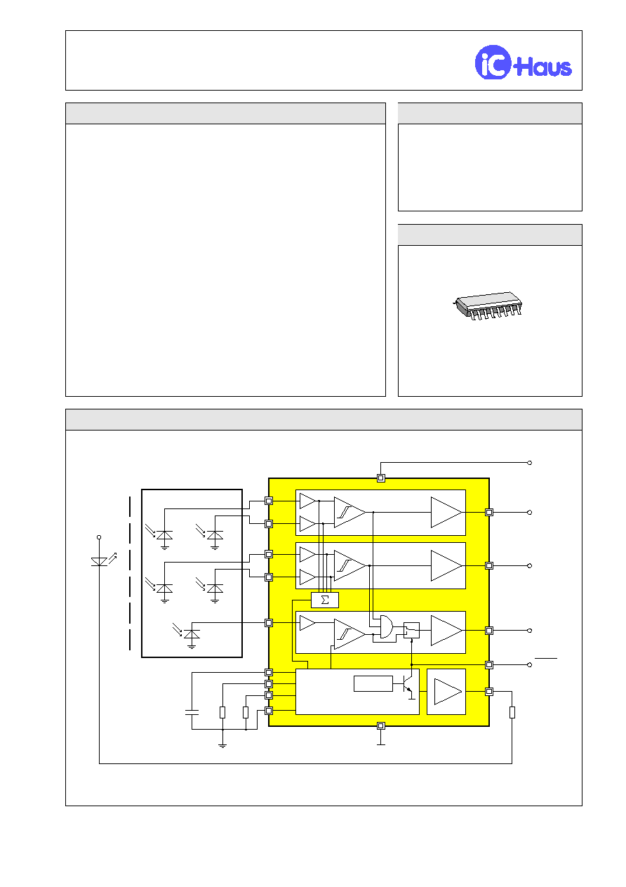
BLOCK DIAGRAM
�1997
Rev A0
PHOTODIODES ARRAY
CODEWHEEL
+5V
+5V
OUT_A
OUT_B
OUT_Z
ERROR
DRIVER
LED
LED CURRENT CONTROL
ERROR
TRACK A
TRACK B
TRACK Z
DPB
DPA
DZ
RLED
68
RLR
15k
DNB
DNA
CLR
10nF
15k
RZ
LED
16
AGND
3
A
7
LED
6
NERR
4
B
5
Z
2
VCC
1
GND
11
DZ
14
DPA
15
DNA
12
DPB
13
DNB
8
CLR
10
ILR
9
iC-WT
IZ
iC-OR
iC-Haus GmbH
Tel
+49-6135-9292-0
Integrated Circuits
Fax +49-6135-9292-192
Am Kuemmerling 18, D-55294 Bodenheim
http://www.ichaus.com
iC-WT
INCREMENTAL ENCODER
Rev A0, Page 2/13
DESCRIPTION
The device iC-WT is an evaluator IC for optical increment linear and rotary motion sensors, e.g. glass
scales or shaft encoders.
A photodiodes array supplies the input signals for the monolithically integrated amplifiers, comparators and
the TTL compatible push-pull output drivers. Two tracks, A and B, are evaluated differentially, the index
track Z as a constant light.
An integrated LED current control with driver stage enables the direct connection of a transmit LED with
series resistor and ensures a constant optical receive power. Two external resistors are used to set the
relative index track comparator threshold and to determine the receive photocurrents.
The internally available logical AND operation of index track Z to tracks A and B can be switched off for
adjustment.
A monitor circuit triggers an error message when the LED current control range is violated. The fault output
designed as an open collector is low active and simultaneously functions as an input to turn off the AND
operation of the index track.
All connections are protected against damage due to ESD. The outputs are short-circuit proof.
PACKAGES SO16N to JEDEC Standard
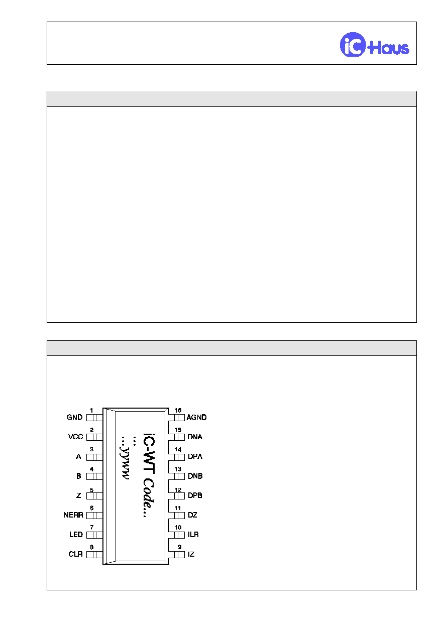
PIN CONFIGURATION SO16N
PIN FUNCTIONS
(top view)
No. Name Function
1
GND
Ground
2
VCC
+5V Supply Voltage
3
A
Track A TTL Output
4
B
Track B TTL Output
5
Z
Track Z TTL Output
6
NERR Fault Output / AND Gate Disable
7
LED
Cathode LED
8
CLR
Capacitor for LED Current Control
9
IZ
Threshold for Index Track
10
ILR
Current Control Adjust
11
DZ
Cathode Photodiode Index Track Z
12
DPB
Cathode Photodiode Track B+
13
DNB
Cathode Photodiode Track B-
14
DPA
Cathode Photodiode Track A+
15
DNA
Cathode Photodiode Track A-
16
AGND Common Anode for all photodiodes,
connected to GND internally

iC-WT
INCREMENTAL ENCODER
Rev A0, Page 3/13
ABSOLUTE MAXIMUM RATINGS
Values beyond which damage may occur; device operation is not guaranteed.
Item
Symbol
Parameter
Conditions
Fig.
Unit
Min.
Max.
G001 VCC
Supply Voltage
0
7
V
G002 I(DPx)
I(DNx)
Current in Inputs
DPA, DNA, DPB, DNB
-1
1
mA
G003 V(A,B,Z)
Voltage at Outputs A, B, Z
0
VCC
G004 I(A,B,Z)
Current in Outputs A, B, Z
V(A,B,Z)< 0V or V(A,B,Z)> VCC
-4
4
mA
G005 I(DZ)
Current in Input DZ
-1
1
mA
G006 I(ILR)
I(IZ)
Current in ILR, IZ
-6
1
mA
G007 I(CLR)
Current in CLR
-1
1
mA
G008 I(LED)
Current in LED
V(LED)> VCC
-1
1
mA
G009 I(LED)
Current in LED
V(LED)
VCC
-1
60
mA
G010 V(NERR) Voltage at NERR
0
VCC
G011 I(NERR)
Current in NERR
V(NERR)< 0 or V(NERR)> VCC
-4
4
mA
TG1 Tj
Junction Temperature
-30
130
�
C
TG2 Ts
Storage Temperature
-30
130
�
C
THERMAL DATA
Operating Conditions: VCC= 5V
�
10%
Item
Symbol
Parameter
Conditions
Fig.
Unit
Min.
Typ.
Max.
T1
Ta
Operating Ambient Temperature
Range
(extended temperature range on
request)
-25
125
�
C
T2
Rthja
Thermal Resistance
Chip to Ambient
SMD mounting, without special
cooling
125
K/W
All voltages are referenced to ground unless otherwise noted.
All currents into the device pins are positive; all currents out of the device pins are negative.
iC-WT
INCREMENTAL ENCODER
Rev A0, Page 4/13
ELECTRICAL CHARACTERISTICS
Operating Conditions: VCC= 5V
�
10%, Tj= -25..125
�
C, unless otherwise noted
Item
Symbol
Parameter
Conditions
Tj
Fig.
Unit
�
C
Min.
Typ.
Max.
Total Device
001
VCC
Permissible Supply Voltage
4.5
5.5
V
002
I(VCC)
Supply Current in VCC,
Outputs A, B, Z hi
closed LED control:
R(ILR/AGND)= 15k
,
I(LED)
3mA, NERR= hi;
I(A,B,Z)= 0, R(RZ/AGND)= 15k
,
I(DZ,DPx)= -400nA,
I(DNx)= -40..0nA, (x= A,B)
10
mA
003
I(VCC)
Supply Current in VCC,
Outputs A, B, Z lo
closed LED control:
R(ILR/AGND)= 15k
,
I(LED)
3mA, NERR= hi;
I(A,B,Z)= 0, R(RZ/AGND)= 15k
,
I(DZ,DPx)= -40..0nA
I(DNx)= -400nA
27
5.5
12
mA
mA
004
fo
Cut-off Frequency
for Tracks A and B
sinusoidal waveform,
I(DPx)= -20..-400nA,
I(DNx)= -400..-20nA
500
kHz
005
fo
Cut-off Frequency
for Index Track Z
rectangular waveform,
I(DZ)= -20..-400nA,
threshold 200nA
250
kHz
006
tp()
Propagation Delay Deviation
track vs.track at A, B, Z
100
ns
Differential Photocurrent Amplifier, Track A and B
101
I(DPx)
I(DNx)
Permissible Sensor Current at
DPA, DNA, DPB, DNB
-600
0
nA
102
CM(P/N) Common Mode DPA vs. DNA,
DPB vs. DNB
0.85
1
1.15
Comparator, Track A and B
201
Hys
Hysteresis refered to [I(DPx) +
I(DNx)] / 2
I(DPx,DNx)= -400..0nA
15
20
25
%
Photocurrent Amplifier, Index Track Z
401
I(DZ)
Permissible Sensor Current at DZ
-600
0
nA
Comparator, Index Track Z
801
Hys
Hysteresis refered to I(DZ)
I(DZ)= -400..0nA
7
10
13
%
Push-Pull Outputs A, B, Z
301
Vs()hi
Saturation Voltage hi
Vs()hi= VB-V();
I()= -400
�
A
-25
27
70
125
0.9
0.8
0.75
0.7
1.1
1.0
0.9
0.9
V
V
V
V
302
Vs()hi
Saturation Voltage hi
Vs()hi= VB-V();
I()= -1.6mA
-25
27
70
125
1.2
1.1
1.05
1.05
1.5
1.4
1.3
1.3
V
V
V
V
303
Vs()lo
Saturation Voltage lo
I()= 0.8mA
0.4
V
304
Vs()lo
Saturation Voltage lo
I()= 1.6mA
0.5
V
305
Isc()hi
Short-Circuit Current hi
V()= 0V..2.8V
27
-8
-3.5
-1.7
mA
mA

iC-WT
INCREMENTAL ENCODER
Rev A0, Page 5/13
ELECTRICAL CHARACTERISTICS
Operating Conditions: VCC= 5V
�
10%, Tj= -25..125
�
C, unless otherwise noted
Item
Symbol
Parameter
Conditions
Tj
Fig.
Unit
�
C
Min.
Typ.
Max.
Push-Pull Outputs A, B, Z (continued)
306
Isc()lo
Short-Circuit Current lo
V()= 1V..VCC
27
2
6
13
mA
mA
307
Vc()hi
Clamp Voltage hi
Vc()hi= V()-VCC; I()= 4mA
0.4
1.5
V
308
Vc()lo
Clamp Voltage lo
I()=-4mA
-1.5
-0.4
V
LED Current Control, pins CLR, ILR, IZ, LED
601
ISUM
Permissible Total Sensor Current
at DPA, DNA, DPB, DNB
ISUM= I(DPA)+I(DNA) +I(DPB)
+I(DNB);
-1500
-50
nA
602
I(LED)
Permissible Driver Current in LED
0.1
50
mA
603
Vs(LED)
Saturation Voltage lo at LED
I(LED)= 50mA,
I(ILR)> 5
�
A, ISUM= 0
27
0.4
0.8
1.2
V
V
604
V(ILR)
V(IZ)
Voltage at ILR, IZ
I(ILR,IZ)= -150..-5
�
A
1.15
1.22
1.28
V
606
Isc(ILR)
Isc(IZ)
Short-Circuit Current in ILR, IZ
V(ILR)= 0, V(IZ)= 0
27
-5
-2.4
mA
mA
607
CR(ILR)
Current Ratio I(ILR)/ISUM
closed LED control,
ISUM= -800..-50nA
80
100
125
608
CR(IZ)
Current Ratio I(IZ)/I(DZ)
closed LED control,
I(DZ)= -400..-10nA
320
400
500
609
Vc()hi
Clamp Voltage hi
at LED, CLR, ILR, IZ
VCC= 0V, I()= 1mA
0.4
1.0
V
610
Vc()lo
Clamp Voltage lo
at LED, CLR, ILR, IZ
VCC= 0V, I()=-1mA
-1.0
-0.4
V
Error Detection, AND Gate Select, Input/Output NERR
501
R(NERR) Internal Pull-Up Resistor
20
30
45
k
502
Vt()Gate
AND Gate Turn-Off Threshold
Gate disabled if V(NERR)< 0.4V
27
0.4
0.5
1
V
V
701
Vs()lo
Saturation Voltage lo
I(NERR)= 1.6mA
27
0.15
0.4
V
V
702
Vs()lo
Saturation Voltage lo
I(NERR)= 5mA
27
0.25
0.8
V
V
703
Isc()lo
Short-Circuit Current lo
V(NERR)= 2V..VCC
27
5
15
30
mA
mA
704
Vc()hi
Clamp Voltage hi
Vc()hi= V(NERR)-VCC;
NERR=hi, I(NERR)= 4mA
0.4
1.5
V
705
Vc()lo
Clamp Voltage lo
NERR=lo, I(NERR)=-4mA
-1.5
-0.4
V