 | –≠–ª–µ–∫—Ç—Ä–æ–Ω–Ω—ã–π –∫–æ–º–ø–æ–Ω–µ–Ω—Ç: iC-XU | –°–∫–∞—á–∞—Ç—å:  PDF PDF  ZIP ZIP |

iC-XU
PROGRAMMABLE QUAD LOW/HIGH SIDE DRIVER
FEATURES
APPLICATIONS
4 independently controllable channels with 8 power output
stages
Power output stages for 350mA continuous current and high
impulse load
Integrated free-wheeling diodes
Microprocessor-compatible drive circuit for up to 4 servo-
motors or loads in half-bridge or 2 motors in full-bridge
operation
TTL-compatible and noise-proof inputs with integrated
clamping diodes
CMOS-compatible due to low input currents
Broad voltage range for unipolar and bipolar supply
Low/high side driver for any
load circuits
4-channel drive circuit for
servomotors
PACKAGES
PDIP22
BLOCK DIAGRAM
©1997
Rev A1
PWM INPUT
+5V
DRIVER INHIBIT
-10V..0V
+5V..20V
VCC
RESET
+12V
iC-XU
LOGIC
LATCH
STROBE
10
µ
F
10
µ
F
SP
17
NP
16
M4-
18
M4+
6
M3-
19
M3+
5
M2-
21
M2+
3
M1-
22
M1+
2
R
14
FHB
13
ND+
7
ND-
8
NCS2
10
NCS1
9
A1
12
A0
11
+VM
4
-VM
20
VCC
15
GND
1
M
1
µ
F
FULL/HALF
iC-Haus GmbH
Tel
+49-6135-9292-0
Integrated Circuits
Fax +49-6135-9292-192
Am Kuemmerling 18, D-55294 Bodenheim
http://www.ichaus.com
iC-XU
PROGRAMMABLE QUAD LOW/HIGH SIDE DRIVER
Rev A1, Page 2/10
DESCRIPTION
The device iC-XU is a universal quadruple low/high side driver for any loads, e.g. lamps and relays, or to
drive servomotors in half- or full-bridge circuit.
Designed especially for use in microprocessor-controlled systems, it features appropriate control, address
and data lines which enable a direct connection to the microprocessor bus. The input interfaces ensure
TTL, CMOS and NMOS compatibility and are immune to short voltage peaks.
In the programmable half-bridge mode (FHB= 0) the device can drive as many as four motors via inte-
grated push-pull power output stages. In the full-bridge mode (FHB= 1) two motors are operated from
output stages driven in phase opposition.
The current operating state of the output stages is stored in the associated flipflops. Via inputs SP or NP,
all output stages can also be blocked or pulsed simultaneously in stored state.
This device is designed for industry applications with the highest quality requirements and is available as a
bipolar IC in a plastic DIL package.
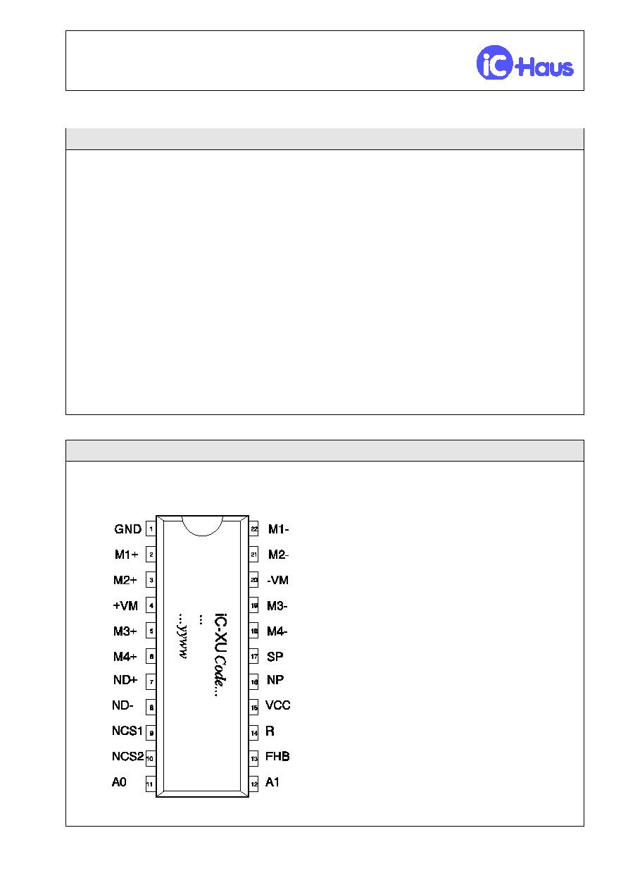
PACKAGES PIDP22 to JEDEC Standard
PIN CONFIGURATION PDIP22
PIN FUNCTIONS
(top view)
No. Name Function
1
GND
Ground
2
M1+
Driver 1 (Source)
3
M2+
Driver 2 (Source)
4
+VM
Pos. Driver Supply Voltage
5
M3+
Driver 3 (Source)
6
M4+
Driver 4 (Source)
7
ND+
Data Input (Source)
8
ND-
Data Input (Sink)
9
NCS1 Chip Select 1, active low
10
NCS2 Chip Select 2, active low
11
A0
Address
12
A1
Address
13
FHB
Full/Half Bridge Select
14
R
Reset
15
VCC
Logic Supply Voltage
16
NP
PWM Input, active low
17
SP
Drivers Inhibit
18
M4-
Driver 4 (Sink)
19
M3-
Driver 3 (Sink)
20
-VM
Neg. Driver Supply Voltage
21
M2-
Driver 2 (Sink)
22
M1-
Driver 1 (Sink)
iC-XU
PROGRAMMABLE QUAD LOW/HIGH SIDE DRIVER
Rev A1, Page 3/10
PROGRAMMING
Half Bridge Mode (FHB= 0)
Inputs
Latches
Drivers
M4
M3
M2
M1
M4
M3
M2
M1
SP
NP
R
NCS1 NCS2
ND-
ND+
A1
A0
-
+
-
+
-
+
-
+
-
+
-
+
-
+
-
+
0
0
0
t
t
1
1
0
0
Q0
Q0
Q0
Q0
Q0
Q0
0
0
Q0
Q0
Q0
Q0
Q0
Q0
off
off
0
0
0
t
t
1
1
0
1
Q0
Q0
Q0
Q0
0
0
Q0
Q0
Q0
Q0
Q0
Q0
off
off
Q0
Q0
0
0
0
t
t
1
1
1
0
Q0
Q0
0
0
Q0
Q0
Q0
Q0
Q0
Q0
off
off
Q0
Q0
Q0
Q0
0
0
0
t
t
1
1
1
1
0
0
Q0
Q0
Q0
Q0
Q0
Q0
off
off
Q0
Q0
Q0
Q0
Q0
Q0
0
0
0
t
t
1
0
0
0
Q0
Q0
Q0
Q0
Q0
Q0
0
1
Q0
Q0
Q0
Q0
Q0
Q0
off
on
0
0
0
t
t
1
0
0
1
Q0
Q0
Q0
Q0
0
1
Q0
Q0
Q0
Q0
Q0
Q0
off
on
Q0
Q0
0
0
0
t
t
1
0
1
0
Q0
Q0
0
1
Q0
Q0
Q0
Q0
Q0
Q0
off
on
Q0
Q0
Q0
Q0
0
0
0
t
t
1
0
1
1
0
1
Q0
Q0
Q0
Q0
Q0
Q0
off
on
Q0
Q0
Q0
Q0
Q0
Q0
0
0
0
t
t
0
1
0
0
Q0
Q0
Q0
Q0
Q0
Q0
1
0
Q0
Q0
Q0
Q0
Q0
Q0
on
off
0
0
0
t
t
0
1
0
1
Q0
Q0
Q0
Q0
1
0
Q0
Q0
Q0
Q0
Q0
Q0
on
off
Q0
Q0
0
0
0
t
t
0
1
1
0
Q0
Q0
1
0
Q0
Q0
Q0
Q0
Q0
Q0
on
off
Q0
Q0
Q0
Q0
0
0
0
t
t
0
1
1
1
1
0
Q0
Q0
Q0
Q0
Q0
Q0
on
off
Q0
Q0
Q0
Q0
Q0
Q0
0
0
0
t
t
0
0
0
0
Q0
Q0
Q0
Q0
Q0
Q0
0
0
Q0
Q0
Q0
Q0
Q0
Q0
off
off
0
0
0
t
t
0
0
0
1
Q0
Q0
Q0
Q0
0
0
Q0
Q0
Q0
Q0
Q0
Q0
off
off
Q0
Q0
0
0
0
t
t
0
0
1
0
Q0
Q0
0
0
Q0
Q0
Q0
Q0
Q0
Q0
off
off
Q0
Q0
Q0
Q0
0
0
0
t
t
0
0
1
1
0
0
Q0
Q0
Q0
Q0
Q0
Q0
off
off
Q0
Q0
Q0
Q0
Q0
Q0
0
0
0
t
1
X
X
X
X
0
0
0
1
t
X
X
X
X
Q0
Q0
0
0
0
1
1
X
X
X
X
0
1
0
1
1
X
X
X
X
1
0
0
1
1
X
X
X
X
Q0
off
1
1
0
1
1
X
X
X
X
X
X
1
X
X
X
X
X
X
0
0
0
0
0
0
0
0
off
off
off
off
off
off
off
off
Full Bridge Mode (FHB= 1)
Inputs
Latches
Drivers
M4
M3
M2
M1
M4
M3
M2
M1
SP
NP
R
NCS1 NCS2
ND-
ND+
A1
A0
-
+
-
+
-
+
-
+
-
+
-
+
-
+
-
+
0
0
0
t
t
1
1
0
0
Q0
Q0
Q0
Q0
0
0
0
0
Q0
Q0
Q0
Q0
on
off
on
off
0
0
0
t
t
1
1
0
1
Q0
Q0
Q0
Q0
Q0
Q0
Q0
Q0
Q0
Q0
Q0
Q0
Q0
Q0
Q0
Q0
0
0
0
t
t
1
1
1
0
Q0
Q0
Q0
Q0
Q0
Q0
Q0
Q0
Q0
Q0
Q0
Q0
Q0
Q0
Q0
Q0
0
0
0
t
t
1
1
1
1
0
0
0
0
Q0
Q0
Q0
Q0
on
off
on
off
Q0
Q0
Q0
Q0
0
0
0
t
t
1
0
0
0
Q0
Q0
Q0
Q0
1
0
0
1
Q0
Q0
Q0
Q0
on
off
off
on
0
0
0
t
t
1
0
0
1
Q0
Q0
Q0
Q0
Q0
Q0
Q0
Q0
Q0
Q0
Q0
Q0
Q0
Q0
Q0
Q0
0
0
0
t
t
1
0
1
0
Q0
Q0
Q0
Q0
Q0
Q0
Q0
Q0
Q0
Q0
Q0
Q0
Q0
Q0
Q0
Q0
0
0
0
t
t
1
0
1
1
1
0
0
1
Q0
Q0
Q0
Q0
on
off
off
on
Q0
Q0
Q0
Q0
0
0
0
t
t
0
1
0
0
Q0
Q0
Q0
Q0
0
1
1
0
Q0
Q0
Q0
Q0
off
on
on
off
0
0
0
t
t
0
1
0
1
Q0
Q0
Q0
Q0
Q0
Q0
Q0
Q0
Q0
Q0
Q0
Q0
Q0
Q0
Q0
Q0
0
0
0
t
t
0
1
1
0
Q0
Q0
Q0
Q0
Q0
Q0
Q0
Q0
Q0
Q0
Q0
Q0
Q0
Q0
Q0
Q0
0
0
0
t
t
0
1
1
1
0
1
1
0
Q0
Q0
Q0
Q0
off
on
on
off
Q0
Q0
Q0
Q0
0
0
0
t
t
0
0
0
0
Q0
Q0
Q0
Q0
0
0
0
0
Q0
Q0
Q0
Q0
on
off
on
off
0
0
0
t
t
0
0
0
1
Q0
Q0
Q0
Q0
Q0
Q0
Q0
Q0
Q0
Q0
Q0
Q0
Q0
Q0
Q0
Q0
0
0
0
t
t
0
0
1
0
Q0
Q0
Q0
Q0
Q0
Q0
Q0
Q0
Q0
Q0
Q0
Q0
Q0
Q0
Q0
Q0
0
0
0
t
t
0
0
1
1
0
0
0
0
Q0
Q0
Q0
Q0
on
off
on
off
Q0
Q0
Q0
Q0
0
0
0
t
1
X
X
X
X
0
0
0
1
t
X
X
X
X
Q0
Q0
0
0
0
1
1
X
X
X
X
0
1
0
1
1
X
X
X
X
on
off
on
off
on
off
on
off
1
0
0
1
1
X
X
X
X
Q0
on
off
on
off
on
off
on
off
1
1
0
1
1
X
X
X
X
on
off
on
off
on
off
on
off
X
X
1
X
X
X
X
X
X
0
0
0
0
0
0
0
0
on
off
on
off
on
off
on
off
1= High Level, 0= Low Level, X= undefined, t: 0
1, Q0= no changes occur,
NSC1, NCS2 active low, NCS1 logical AND gated with NCS2
iC-XU
PROGRAMMABLE QUAD LOW/HIGH SIDE DRIVER
Rev A1, Page 4/10
ABSOLUTE MAXIMUM RATINGS
Values beyond which damage may occur; device operation is not guaranteed.
Item
Symbol
Parameter
Conditions
Fig.
Unit
Min.
Max.
G001 VCC
Logic Supply Voltage
0
6
V
G002 +VM
Pos. Driver Supply Voltage
0
20
V
G003 +VM
Neg. Driver Supply Voltage
-10
0
V
G004 VM
Supply Voltage +VM vs. -VM
0
20
V
G005 I(M+)
Current in M+ (*)
-350
0
mA
G006 I(M-)
Current in M- (*)
0
350
mA
G007 Ipk(M+)
Pulse Current in M+
ton< 100ms, toff= 10
◊
ton
-500
0
mA
G008 Ipk(M-)
Pulse Current in M-
ton< 100ms, toff= 10
◊
ton
0
500
mA
G009 I()
Current in A0, A1, NCS1, NCS2, ND-,
ND+, FHB, R, NP, SP
-8
8
mA
TG1 Pmax
Max. Power Dissipation
PDIP22 package, Ta= 70
∞
C
0.8
W
TG2 Tj
Junction Temperature
-40
150
∞
C
TG3 Ts
Storage Temperature
-40
150
∞
C
(*) M+: M1+..M4+, M-: M1-..M4-
THERMAL DATA
Operating Conditions: +VM= 4..8V, -VM= -8..0V, VCC= 5V
±
10%
Item
Symbol
Parameter
Conditions
Fig.
Unit
Min.
Typ.
Max.
T1
Ta
Operating Ambient Temperature
Range
0
70
∞
C
T2
Rthja
Thermal Resistance
Chip to Ambient
soldered on PCB, with approx. 2cm≤
cooling surface
PDIP22 package
70
K/W
All voltages are referenced to ground unless otherwise noted.
All currents into the device pins are positive; all currents out of the device pins are negative.

iC-XU
PROGRAMMABLE QUAD LOW/HIGH SIDE DRIVER
Rev A1, Page 5/10
ELECTRICAL CHARACTERISTICS
Operating Conditions:
VCC= 5V
±
10%, +VM= 4..8V, -VM= -8..0V, Tj= 0..125
∞
C, unless otherwise noted.
Item
Symbol
Parameter
Conditions
Tj
Fig.
Unit
∞
C
Min.
Typ.
Max.
Total Device
001
VCC
Permissible Supply Voltage
Range at VCC
4.5
5.5
V
002
I(VCC)
Supply Current in VCC
M-: off
27
70
9.5
8.6
20
mA
mA
mA
003
I(VCC)
Supply Current in VCC
M-: on, -VM= -8..-5V
27
70
9.5
8.6
20
mA
mA
mA
004
I(VCC)
Supply Current in VCC
M-: on, -VM= -5..0V
27
70
83
63
120
mA
mA
mA
005
VM
Permissible Supply Voltage
Range at +VM to -VM
4
16
V
006
I(+VM)
Supply Current in +VM
M+: off
80
µ
A
007
I(+VM)
Supply Current in +VM
M+: on, +VM= 20V, -VM to GND
5
mA
008
I(-VM)
Supply Current in -VM
M-: off, -VM= -8V
27
-5
-2
mA
mA
009
I(-VM)
Supply Current in -VM
M-: on, -VM= -8V
27
70
-120
-74
-54
mA
mA
mA
Inputs A0, A1, NCS1, NSC2, ND+, ND-, FHB, R, NP, SP
101
Vt()hi
Threshold Voltage hi
VCC= 5V
2
V
102
Vt()lo
Threshold Voltage lo
VCC= 5V
0.8
V
103
I()hi
Input Current hi
V()= 2.7V
20
µ
A
104
I()lo
Input Current lo
V()= 0.4V
-100
µ
A
105
Vc()hi
Clamp Voltage hi
I()= 5mA
27
70
7.6
7.9
8.5
V
V
V
106
Vc()lo
Clamp Voltage lo
I()= -5mA
27
70
-1.5
-0.88
-0.80
V
V
V
107
tp
(NCS-M)
Switch Delay NCS1 or NCS2 to
M+ resp. M-
27
2
4
7
µ
s
µ
s
Driver Outputs M+, M-
201
Vs()hi
Saturation Voltage hi at M+
Vs()hi= +VM - V(M+);
I(M+)= -500mA
27
70
1.2
1.1
2.5
V
V
V
202
Vs()hi
Saturation Voltage hi at M+
Vs()hi= +VM - V(M+);
I(M+)= -350mA
27
0.9
1.2
V
203
Vs()lo
Saturation Voltage lo at M-
Vs()lo= V(M-) - (-VM);
I(M-)= 500mA
27
70
0.80
0.85
2.5
V
V
V
204
Vs()lo
Saturation Voltage lo at M-
Vs()hi= V(M-) - (-VM);
I(M-)= 350mA
27
0.7
1.2
V
V
205
I0()
Leakage Current in M+
M+: off
27
-20
1
20
µ
A
µ
A
206
I0()
Leakage Current in M-
M-: off
27
-20
1
20
µ
A
µ
A