
IC42S16400
Integrated Circuit Solution Inc.
1
DR034-0E 12/02/2003
Document Title
1M x 16Bit x 4 Banks (64-MBIT) SDRAM
Revision History
Revision No
History
Draft Date
Remark
0A
Initial Draft
Demcember 20,2001
0B
Revise DC OPERATING CONDITIONS
April 15,2002
0C
1.add -6ns speed grade
Novembver 22,2002
2.obsolete 8Mx8 configuration
3.obsolete Low power version
4.obsolete -8ns speed grade
0D
Add 60 ball(64M SDRAM) VF-BGA package
September 05,2003
0E
Add Pb-free package
December 02,2003
The attached datasheets are provided by ICSI. Integrated Circuit Solution Inc reserve the right to change the specifications and
products. ICSI will answer to your questions about device. If you have any questions, please contact the ICSI offices.
IC42S16400
2
Integrated Circuit Solution Inc.
DR034-0E 12/02/2003
ICSI reserves the right to make changes to its products at any time without notice in order to improve design and supply the best possible product. We assume no responsibility for any errors
which may appear in this publication. � Copyright 2000, Integrated Circuit Solution Inc.
FEATURES
� Single 3.3V (
�
0.3V) power supply
� High speed clock cycle time -6: 166MHz,
-7: 133MHz<3-3-3>
� Fully synchronous operation referenced to clock
rising edge
� Possible to assert random column access in
every cycle
� Quad internal banks contorlled by A12 & A13
(Bank Select)
� Byte control by LDQM and UDQM for
IC42S16400
� Programmable Wrap sequence (Sequential /
Interleave)
� Programmable burst length (1, 2, 4, 8 and full
page)
� Programmable CAS latency (2 and 3)
� Automatic precharge and controlled precharge
� CBR (Auto) refresh and self refresh
� LVTTL compatible inputs and outputs
� 4,096 refresh cycles / 64ms
� Burst termination by Burst stop and Precharge
command
� Package 400mil 54-pin TSOP-2 and 60ball(64M)
VF-BGA
� Pb(lead)-free package is available
DESCRIPTION
The IC42S16400 are high-speed 67,108,864-bit syn-
chronous dynamic random-access memories, orga-
nized as 1,048,576 x 16 x 4 (word x bit x bank),
respectively.
The synchronous DRAMs achieved high-speed data
transfer using the pipeline architecture and clock
frequency up to 166MHz for -6. All input and outputs are
synchronized with the positive edge of the clock.The
synchronous DRAMs are compatible with Low Voltage
TTL (LVTTL).These products are packaged in 54-pin
TSOP-2 and 60ball(64M) VF-BGA.
1M x 16 Bits x 4 Banks (64-MBIT)
SYNCHRONOUS DYNAMIC RAM
1
2
3
4
5
6
7
8
9
10
11
12
13
14
15
16
17
18
19
20
21
22
23
24
25
26
27
54
53
52
51
50
49
48
47
46
45
44
43
42
41
40
39
38
37
36
35
34
33
32
31
30
29
28
VDD
DQ0
VDDQ
DQ1
DQ2
VSSQ
DQ3
DQ4
VDDQ
DQ5
DQ6
VSSQ
DQ7
VDD
LDQM
WE
CAS
RAS
CS
BA0
BA1
A10
A0
A1
A2
A3
VDD
VSS
DQ15
VSSQ
DQ14
DQ13
VDDQ
DQ12
DQ11
VSSQ
DQ10
DQ9
VDDQ
DQ8
VSS
NC
UDQM
CLK
CKE
NC
A11
A9
A8
A7
A6
A5
A4
VSS
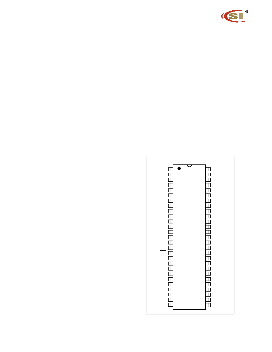
PIN CONFIGURATIONS
54-Pin TSOP-2
IC42S16400
Integrated Circuit Solution Inc.
3
DR034-0E 12/02/2003
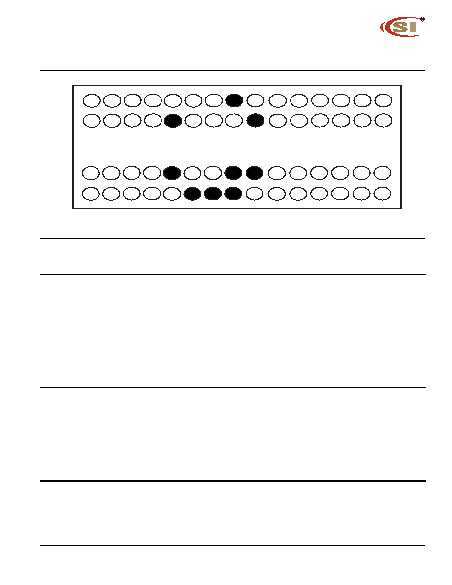
60-BALL VF-BGA ( 64M SDRAM )
R P N M L K J H G F E D C B A
VSS
A4
A6
A5
A8
A7
A11
A9
CKE
NC
NC
CLK
NC
UDQM
NC
NC
A3
VDD
A2
A1
A0
A10
BA1
BA0
NC
CS
RAS
CAS
LDQM
WE
NC
DQ8
NC
DQ9
VDDQ
DQ
10
VSSQ
DQ
12
DQ
11
DQ
13
VDDQ
NC
DQ7
VSSQ
DQ6
VDDQ
DQ5
DQ4
DQ3
VSSQ
DQ2
DQ
14
VSSQ
VSS
DQ
15
V
DDQ
DQ1
DQ0
VDD
7
6
5
4
3
2
1
VDD
PIN DESCRIPTIONS
A0 - A11
Address
Row Address : RA0 - RA11, Column Address : CA0 - CA7
Auto-precharge flag : A10
BA0,BA1
Bank Address
Selects bank to be activated during RAS activity
Selects bank to be read/written during CAS activity
DQ0 - DQ15
Data Input/Output
Multiplexed data input / output pin
CLK
Clock
The system clock input.All other inputs are registered to the SDRAM
on the rising edge of CLK
CKE
Clock Enable
Controls internal clock signal and when deactivated,the SDRAM will
be one of the states among power down,suspend or self refresh
CS
Chip Select
Enables or disables all inputs except CLK, CKE and DQM
RAS
Row Address Strobe
RAS,CAS and WE define the operation
CAS
Column Address Strobe
Refer function truth table for details
WE
Write Enable
LDQM,UDQM
Data Input/Output Mask
Controls output buffers in read mode and masks input data in write
mode
V
DD
/V
SS
Power Supply/Ground
Power supply for internal circuits and input buffers
V
DD
Q/V
SS
Q
Data Output Power/Ground
Power supply for output buffers
NC
No Connection
No Connection
IC42S16400
4
Integrated Circuit Solution Inc.
DR034-0E 12/02/2003
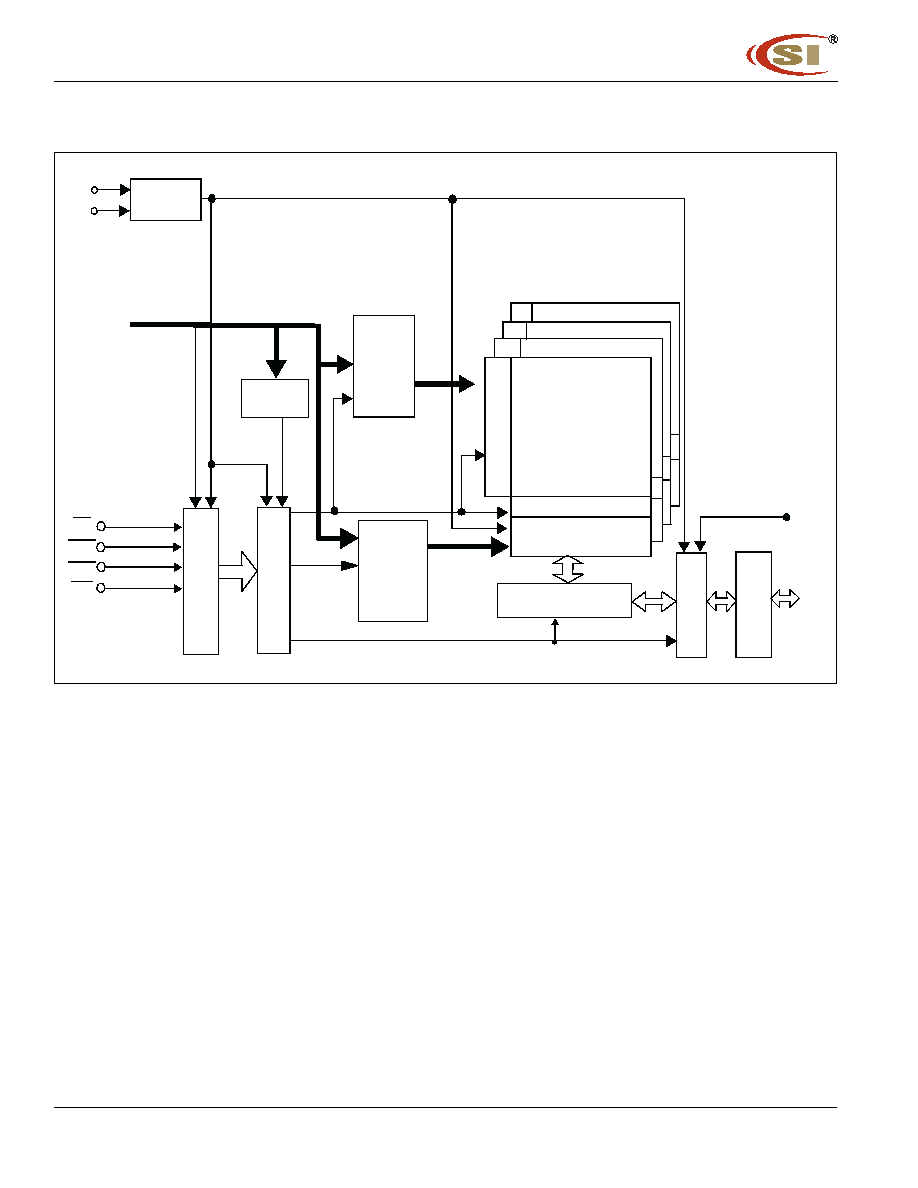
FUNCTIONAL BLOCK DIAGRAM
CLK
CKE
Clock
Generator
CS
RAS
Mode
Register
Column
Address
Buffer
&
Burst
Counter
CAS
WE
C
o
mm
and D
e
c
ode
r
C
ont
r
o
l
Lo
gic
Address
Row
Address
Buffer
&
Refresh
Counter
Bank B
Bank A
Sense Amplifier
Column Decoder &
Latch Circuit
R
o
w
D
e
c
oder
Data Control Circuit
DQ
DQM
La
tc
h
C
i
r
c
ui
t
In
put
&
O
u
t
p
ut
Bu
f
f
e
r
Bank C
Bank D
IC42S16400
Integrated Circuit Solution Inc.
5
DR034-0E 12/02/2003
ABSOLUTE MAXIMUM RATINGS
(1)
Symbol
Parameters
Rating
Unit
V
DD
Supply Voltage (with respect to V
SS
)
�0.5 to +4.6
V
V
DDQ
Supply Voltage for Output (with respect to V
SSQ
)
�0.5 to +4.6
V
V
I
Input Voltage
(with respect to V
SS
)
�0.5 to V
DD
+0.5
V
V
O
Output Voltage
(with respect to V
SSQ
)
�1.0 to V
DDQ
+0.5
V
I
O
Short circuit output current
50
mA
P
D
Power Dissipation (
T
A
= 25 �C)
1
W
T
OPT
Operating Temperature
0 to +70
�C
T
STG
Storage Temperature
�65 to +150
�C
Notes:
1. Exposing the device to stress above those listed in Absolute Maximum Ratings could cause permanent
damage. The device is not meant to be operated under conditions outside the limits described in the
operational section of this specification. Exposure to Absolute Maximum Rating conditions for extended
periods may affect device reliability.
DC RECOMMENDED OPERATING CONDITIONS
(
At T
A
= 0 to +70�C unless otherwise noted)
Symbol
Parameter
Min.
Typ.
Max.
Unit
V
DD
Supply Voltage
3.0
3.3
3.6
V
V
DDQ
Supply Voltage for DQ
3.0
3.3
3.6
V
V
IH
High Level Input Voltage (all Inputs)
2.0
--
V
DD
+ 0.3
V
V
IL
Low Level Input Voltage (all Inputs)
-0.3
--
+0.8
V
CAPACITANCE CHARACTERISTICS
(At T
A
= 0 ~ 70�C, V
DD
= V
DDQ
= 3.3 � 0.3V, V
SS
= V
SSQ
= 0V , unless otherwise noted)
Symbol
Parameter
Min.
Max.
Unit
C
IN
Input Capacitance, address & control pin
2.5
3.8
pF
C
CLK
I
nput Capacitance, CLK pin
2.5
3.5
pF
C
I
/
O
Data Input/Output Capacitance
4.0
6.5
pF
IC42S16400
6
Integrated Circuit Solution Inc.
DR034-0E 12/02/2003
DC ELECTRICAL CHARACTERISTICS
(At T
A
= 0 ~ 70�C, V
DD
= V
DDQ
= 3.3 � 0.3V, V
SS
= V
SSQ
= 0V , unless otherwise noted)
Symbol Parameter
Test Condition
Speed
Min.
Max.
Unit
I
CC
1
(1)
Operating Current
One Bank
active
,
CAS latency = 3
-6(42S16400)
--
95
mA
Burst Length=1
-7(42S16400)
--
85
mA
t
RC
= t
RC
(min.)
t
CLK
= t
CLK
(min.)
I
CC
2P
Precharge Standby Current
CKE < V
IL
(
MAX
)
t
CK
= 15 ns
-6
--
2
mA
(In Power-Down Mode)
-7
--
2
mA
I
CC
2PS
CKE < V
IL
(
MAX
)
CLK < V
IL
(
MAX
)
-6
--
1
mA
-7
--
1
mA
I
CC
2N
(2)
Precharge Standby Current
CS > V
CC
-0.2V
t
CK
= 15 ns
-6
--
20
mA
(In Non Power-Down Mode)
CKE > V
IH
(
MIN
)
-7
--
20
mA
I
CC
2NS
CS > V
CC
-0.2V
CKE < V
IL
(
MAX
)
-6
--
15
mA
CKE > V
IH
(
MIN
)
All input signals are stable.
-7
--
15
mA
I
CC
3P
Active Standby Current
CKE < V
IL
(
MAX
)
t
CK
= 10 ns
-6
--
7
mA
(In Power-Down Mode)
-7
--
7
mA
I
CC
3PS
CKE < V
IL
(
MAX
)
CLK < V
IL
(
MAX
)
-6
--
5
mA
-7
--
5
mA
I
CC
3N
(2)
Active Standby Current
CS > V
CC
-0.2V
t
CK
= 15 ns
-6
--
30
mA
(In Non Power-Down Mode)
CKE > V
IH
(
MIN
)
-7
--
30
mA
I
CC
3NS
CS > V
CC
-0.2V
CKE < V
IL
(
MAX
)
-6
--
25
mA
CKE > V
IH
(
MIN
)
All input signals are stable.
-7
--
25
mA
I
CC
4
Operating Current
All Banks active
CAS latency = 3
-6(42S16400)
--
130
mA
(In Burst Mode)
Burst Length=1
-7(42S16400)
--
100
mA
t
CK
= t
CK
(
MIN
)
I
CC
5
Auto-Refresh Current
t
RC
= t
RC
(
MIN
)
-6
--
150
mA
t
CLK
= t
CLK
(
MIN
)
-7
--
130
mA
I
CC
6
(3, 4)
Self-Refresh Current
CKE < 0.2V
-6
--
1
mA
-7
--
1
mA
I
IL
Input Leakage Current
0V < V
IN
< V
DD
(
MAX
)
�5
5
�A
(Inputs)
Pins not under test = 0V
I
OL
Output Leakage Current
Output is disabled
DQ# in H - Z.,
�5
5
�A
(I/O pins)
0V < V
OUT
< V
DD
(
MAX
)
V
OH
High Level Output Voltage
I
OUT
= �2 mA
2.4
--
V
V
OL
Low Level Output Voltage
I
OUT
= +2 mA
--
0.4
V
Notes:
1. I
CC
(max) is specified at the output open condition.
2. Input signals are changed one time during 30ns.
IC42S16400
Integrated Circuit Solution Inc.
7
DR034-0E 12/02/2003
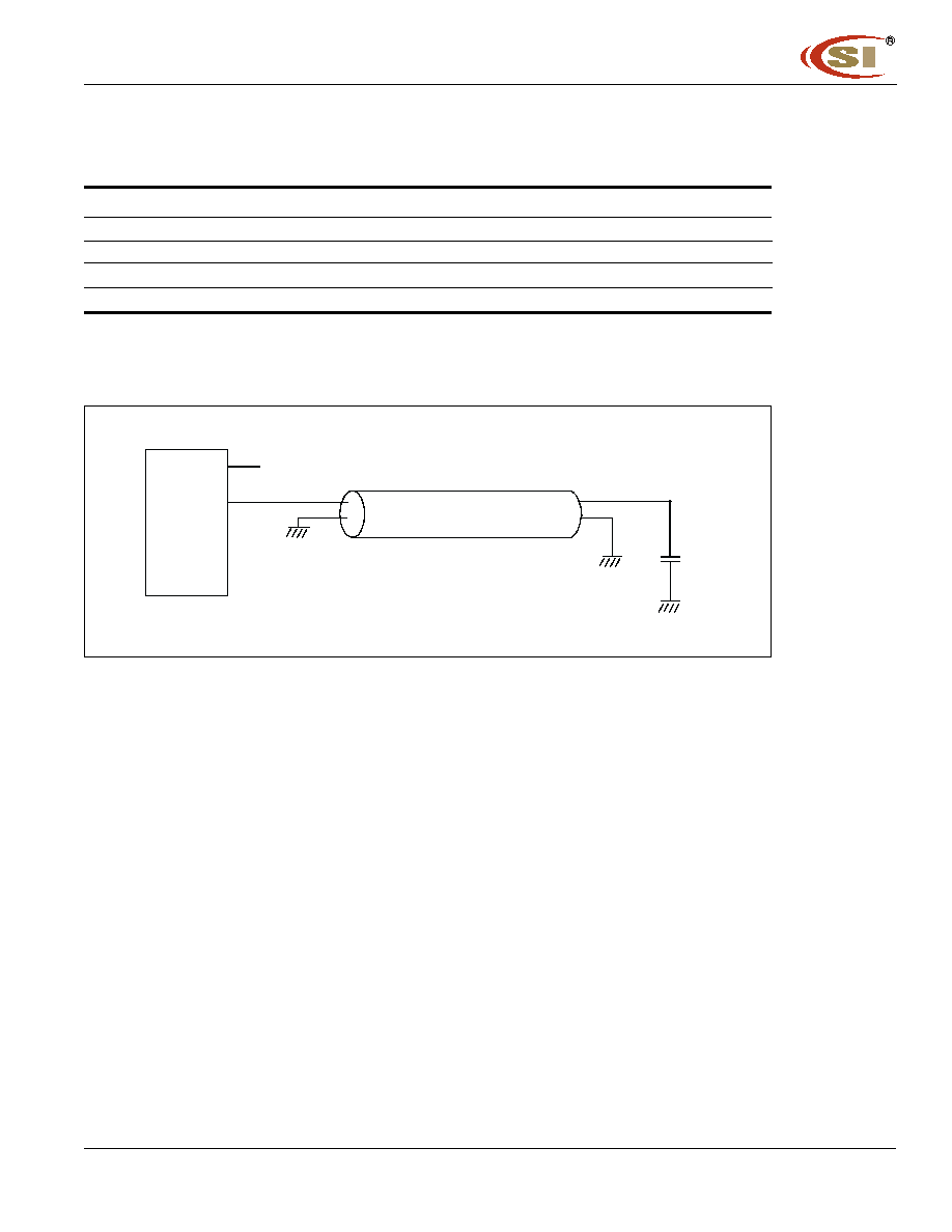
AC TEST CONDITIONS
(At T
A
= 0 ~ 70�C, V
DD
= V
DDQ
= 3.3 � 0.3V, V
SS
= V
SSQ
= 0V , unless otherwise noted)
Parameter
Rating
Unit
AC input Levels (V
IH
/V
IL
)
2.0 / 0.8
V
Input timing reference level /Output timing reference level
1.4
V
Input rise and fall time
1
ns
Output load condition
50
pF
V
DDQ
V
DDQ
V
OUT
Device
Under
Test
50PF
Z = 50
Output Load Conditions

IC42S16400
8
Integrated Circuit Solution Inc.
DR034-0E 12/02/2003
AC ELECTRICAL CHARACTERISTICS
(At T
A
= 0 ~ 70�C, V
DD
= V
DDQ
= 3.3 � 0.3V, V
SS
= V
SSQ
= 0V , unless otherwise noted)
-6
-7
Symbol Parameter
Min.
Max.
Min.
Max.
Units
t
CK
3
CLK Cycle Time
CAS Latency = 3
6
--
7.5
--
ns
t
CK
2
CAS Latency = 2
7.5
--
10
--
ns
t
AC
3
CLK to valid output delay
(1)
CAS Latency = 3
--
5
--
5.4
ns
t
AC
2
CAS Latency = 2
--
6
--
6
ns
t
CH
CLK high pulse width
2.5
--
2.5
--
ns
t
CL
CLK low pulse width
2.5
--
2.5
--
ns
t
CKE
CKE setup time
1.5
--
1.5
--
ns
t
CKH
CKE hold time
0.8
--
0.8
--
ns
t
AS
Address setup time
1.5
--
1.5
--
ns
t
AH
Address hold time
0.8
--
0.8
--
ns
t
CMS
Command setup time
1.5
--
1.5
--
ns
t
CMH
Command hold time
0.8
--
0.8
--
ns
t
DS
Data input setup time
1.5
--
1.5
--
ns
t
DH
Data input hold time
0.8
--
0.8
--
ns
t
OH
3
Output data hold time
(1)
CAS Latency = 3 2.5 -- 2.7 -- ns
t
OH
2 CAS Latency = 2
2.5 -- 3 -- ns
t
LZ
CLK to output in low - Z
0
--
0
--
ns
t
HZ
CLK to output in H - Z
2.5
5
2.7
5.4
ns
t
RC
ROW cycle time
60
--
67.5
--
ns
t
RAS
ROW active time
42
100,000
45
100,000
ns
t
RCD
RAS to CAS delay
18
--
20
--
ns
t
RP
Row precharge time
15
--
20
--
ns
t
RRD
Row active to active delay
12
--
15
--
ns
t
DPL
Data in to precharge
12
--
15
--
ns
t
T
Transition time
1
10
1
10
ns
t
RSC
Mode reg. set cycle
10
--
10
--
ns
t
PDE
Power down exit setup time
7.5
--
7.5
--
ns
t
SRX
Self refresh exit time
7.5
--
7.5
--
ns
t
REF
Refresh Time
--
64
--
64
ms
Notes:
1. if clock rising time is longer than 1ns, (tr/2-0.5ns) should be added to the parameter.

IC42S16400
Integrated Circuit Solution Inc.
9
DR034-0E 12/02/2003
Basic Features and Function Description
Simplified State Diagram
Self
Refresh
MRS
Mode
Register
Set
IDLE
AUTO
Refresh
REF
AC
T
CKE
CKE
B
S
T
Power
Down
Active
Power
Down
ROW
ACTIVE
Read
CKE
CKE
READ
READ
SUSPEND
CKE
CKE
READ A
READA
SUSPEND
Read with
Auto Precharge
CKE
CKE
Write (Write recovery)
WRITE
WRITE
SUSPEND
WRITE A
WRITE A
SUSPEND
CKE
CKE
Write with
Auto Precharge
POWER
ON
Precharge
Precharge
P
R
E
(P
re
ch
a
rg
e
te
rm
in
a
tio
n
)
P
R
E
(
P
re
ch
a
rg
e
t
e
rm
in
a
tio
n
)
R
e
a
d
w
ith
W
ri
te
w
ith
A
u
to
p
re
ch
a
rg
e
A
ut
o
P
re
ch
ar
ge
Re
ad
B
S
T
Wr
ite
Read
with
Au
to Pre
charg
e (
write r
ecove
ry)
Wri
te w
ith
Au
to P
rec
har
ge
Write
Read (write recovery)
PR
E
CK
E
CK
E
Automatic sequence
Manual input
Note: After the AUTO refresh operation, precharge operation is
performed automatically and enter the IDLE state
SE
LF
e
nt
ry
SE
LF
e
xit
Wr
ite
re
co
ve
ry
IC42S16400
10
Integrated Circuit Solution Inc.
DR034-0E 12/02/2003
COMMAND TRUTH TABLE
CKE
A11
Symbol
Command
n-1
n
CS
CS
CS
CS
CS
RAS
RAS
RAS
RAS
RAS
CAS
CAS
CAS
CAS
CAS
WE
WE
WE
WE
WE
BA
A10 A9-A0
DESL
Device deselect
H
X
H
X
X
X
X
X
X
NOP
No operation
H
X
L
H
H
H
X
X
X
MRS
Mode register set
H
X
L
L
L
L
L
L
V
ACT
Bank activate
H
X
L
L
H
H
V
V
V
READ
Read
H
X
L
H
L
H
V
L
V
READA
Read with auto precharge
H
X
L
H
L
H
V
H
V
WRIT
Write
H
X
L
H
L
L
V
L
V
WRITA
Write with auto precharge
H
X
L
H
L
L
V
H
V
PRE
Precharge select bank
H
X
L
L
H
L
V
L
X
PALL
Precharge all banks
H
X
L
L
H
L
X
H
X
BST
Burst stop
H
X
L
H
H
L
X
X
X
REF
CBR (Auto) refresh
H
H
L
L
L
H
X
X
X
SELF
Self refresh
H
L
L
L
L
H
X
X
X
Notes:
H : High level
L : Low level
X : High or Low level (Don't care)
V : Valid Data input
DQM TRUTH TABLE
CKE
Symbol
Command
n-1
n
DQM
ENB
Data Write / Output Enable
H
X
L
MASK
Data Mask / Output Disable
H
X
H
CKE TRUTH TABLE
CKE
Symbol
Command
Current State
n-1
n
CS
CS
CS
CS
CS
RAS
RAS
RAS
RAS
RAS
CAS
CAS
CAS
CAS
CAS
WE
WE
WE
WE
WE
Addreess
--
Clock suspend mode entry
Activating
H
L
X
X
X
X
X
--
Clock suspend
Any
L
L
X
X
X
X
X
--
Clock suspend mode exit
Clock suspend
L
H
X
X
X
X
X
REF
CBR refresh command
Idle
H
H
L
L
L
H
X
SELF
Self refresh entry
Idle
H
L
L
L
L
H
X
--
Self refresh exit
Self refresh
L
H
L
H
H
H
X
L
H
H
X
X
X
X
--
Power down entry
Idle
H
L
X
X
X
X
X
--
Power down exit
Power down
L
H
X
X
X
X
X

IC42S16400
Integrated Circuit Solution Inc.
11
DR034-0E 12/02/2003
OPERATION COMMAND TABLE
(1)
Current State Command
Operation
CS
CS
CS
CS
CS
RAS
RAS
RAS
RAS
RAS
CAS
CAS
CAS
CAS
CAS
WE
WE
WE
WE
WE
Address
Idle
DESL
NOP or Power-Down
(2)
H
X
X
X
X
NOP or BST
NOP or Power-Down
(2)
L
H
H
X
X
READ / READA
Illegal
(3)
L
H
L
H
BA, CA, A10
WRIT/WRITA
Illegal
(3)
L
H
L
L
BA, CA, A10
ACT
Row Active
L
L
H
H
BR, RA
PRE/PALL
NOP
L
L
H
L
BA, A10
REF/SELF
Refresh or Self-Refresh
(4)
L
L
L
H
X
MRS
Mode Register Set
L
L
L
L
Op-Code
Row Active
DESL
NOP
H
X
X
X
X
NOP or BST
NOP
L
H
H
H
X
READ/READA
Begin read : Determine AP
(5)
L
H
L
H
BA, CA, A10
WRIT/WRITA
Begin write : Determine AP
(5)
L
H
L
L
BA, CA, A10
ACT
Illegal
(3)
L
L
H
H
BR, RA
PRE/PALL
Precharge
(6)
L
L
H
L
BA, A10
REF/SELF
Illegal
L
L
L
H
X
MRS
Illegal
L
L
L
L
Op-Code
Read
DESL
Continue burst to end -> Row active
H
X
X
X
X
NOP
Continue burst to end -> Row active
L
H
H
H
X
BST
Burst stop -> Row active
L
H
H
L
X
READ/READA
Term burst, new read : Determine AP
(7)
L
H
L
H
BA, CA, A10
WRIT/WRITA
Term burst, start write : Determine AP
(7, 8)
L
H
L
L
BA, CA, A10
ACT
Illegal
(3)
L
L
H
H
BR, RA
PRE/PALL
Term burst, precharging
L
L
H
L
BA, A10
REF/SELF
Illegal
L
L
L
H
X
MRS
Illegal
L
L
L
L
Op-Code
Write
DESL
Continue burst to end -> write recovering
H
X
X
X
X
NOP
Continue burst to end -> write recovering
L
H
H
H
X
BST
Burst stop -> Row active
L
H
H
L
X
READ/READA
Term burst, start read : Determine AP
(7, 8)
L
H
L
H
BA, CA, A10
WRIT/WRITA
Term burst, new write : Determine AP
(7)
L
H
L
L
BA, CA, A10
ACT
Illegal
(3)
L
L
H
H
BR, RA
PRE/PALL
Term burst, precharging
(9)
L
L
H
L
BA, A10
REF/SELF
Illegal
L
L
L
H
X
MRS
Illegal
L
L
L
L
Op-Code
Read With
DESL
Continue burst to end -> Precharging
H
X
X
X
X
Auto-
NOP
Continue burst to end -> Precharging
L
H
H
H
X
Precharge
BST
Illegal
L
H
H
L
X
READ/READA
Illegal
(11)
L
H
L
H
BA, CA, A10
WRIT/WRITA
Illegal
(11)
L
H
L
L
BA, CA, A10
ACT
Illegal
(3)
L
L
H
H
BR, RA
PRE/PALL
Illegal
(11)
L
L
H
L
BA, A10
REF/SELF
Illegal
L
L
L
H
X
MRS
Illegal
L
L
L
L
Op-Code

IC42S16400
12
Integrated Circuit Solution Inc.
DR034-0E 12/02/2003
OPERATION COMMAND TABLE
(continue)
Current State Command
Operation
CS
CS
CS
CS
CS
RAS
RAS
RAS
RAS
RAS
CAS
CAS
CAS
CAS
CAS
WE
WE
WE
WE
WE
Address
Write with auto
DESL
Continue burst to end -> write recovering with auto precharge
H
X
X
X
X
precharge
NOP
Continue burst to end -> write recovering with auto precharge
L
H
H
H
X
BST
Illegal
L
H
H
L
X
READ / READA
Illegal
(11)
L
H
L
H
BA, CA, A10
WRIT/WRITA
Illegal
(11)
L
H
L
L
BA, CA, A10
ACT
Illegal
(3, 11)
L
L
H
H
BR, RA
PRE/PALL
Illegal
(3, 11)
L
L
H
L
BA, A10
REF/SELF
Illegal
L
L
L
H
X
MRS
Illegal
L
L
L
L
Op-Code
Precharging
DESL
Nop -> Enter idle after t
RP
H
X
X
X
X
NOP
Nop -> Enter idle after t
RP
L
H
H
H
X
BST
Nop -> Enter idle after t
RP
L
H
H
L
X
READ/READA
Illegal
(3)
L
H
L
H
BA, CA, A10
WRIT/WRITA
Illegal
(3)
L
H
L
L
BA, CA, A10
ACT
Illegal
(3)
L
L
H
H
BR, RA
PRE/PALL
Nop -> Enter idle after t
RP
L
L
H
L
BA, A10
REF/SELF
Illegal
L
L
L
H
X
MRS
Illegal
L
L
L
L
Op-Code
Row activating
DESL
Nop - > Enter row active after t
RCD
H
X
X
X
X
NOP
Nop - > Enter row active after t
RCD
L
H
H
H
X
BST
Nop - > Enter row active after t
RCD
L
H
H
L
X
READ/READA
Illegal
(3)
L
H
L
H
BA, CA, A10
WRIT/WRITA
Illegal
(3)
L
H
L
L
BA, CA, A10
ACT
Illegal
(3, 9)
L
L
H
H
BR, RA
PRE/PALL
Illegal
(3)
L
L
H
L
BA, A10
REF/SELF
Illegal
L
L
L
H
X
MRS
Illegal
L
L
L
L
Op-Code
Write
DESL
Nop -> Enter row active after t
DPL
H
X
X
X
X
recovering
NOP
Nop -> Enter row active after t
DPL
L
H
H
H
X
BST
Nop -> Enter row active after t
DPL
L
H
H
L
X
READ/READA
Start read, Determine AP
(8)
L
H
L
H
BA, CA, A10
WRIT/WRITA
New write, Determine AP
L
H
L
L
BA, CA, A10
ACT
Illegal
(3)
L
L
H
H
BR, RA
PRE/PALL
Illegal
(3)
L
L
H
L
BA, A10
REF/SELF
Illegal
L
L
L
H
X
MRS
Illegal
L
L
L
L
Op-Code

IC42S16400
Integrated Circuit Solution Inc.
13
DR034-0E 12/02/2003
OPERATION COMMAND TABLE
(continue)
Current State Command
Operation
CS
CS
CS
CS
CS
RAS
RAS
RAS
RAS
RAS
CAS
CAS
CAS
CAS
CAS
WE
WE
WE
WE
WE
Address
Write
DESL
Nop -> Enter precharge after t
DPL
H
X
X
X
X
recovering
NOP
Nop -> Enter precharge after t
DPL
L
H
H
H
X
with auto
BST
Nop -> Enter precharge after t
DPL
L
H
H
L
X
precharge
READ/READA
Illegal
(3 ,8, 11)
L
H
L
H
BA, CA, A10
WRIT/WRITA
Illegal
(3,11)
L
H
L
L
BA, CA, A10
ACT
Illegal
(3, 11)
L
L
H
H
BR, RA
PRE/PALL
Illegal
(3, 11)
L
L
H
L
BA, A10
REF/SELF
Illegal
L
L
L
H
X
MRS
Illegal
L
L
L
L
Op-Code
Auto
DESL
Nop Enter idle after t
RC
H
X
X
X
X
Refreshing
NOP/BST
Nop Enter idle after t
RC
L
H
H
X
X
READ/WRIT
Illegal
L
H
L
X
X
ACT/PRE/PALL
Illegal
L
L
H
X
X
REF/SELF/MRS
Illegal
L
L
L
X
X
Mode
DESL
Nop -> Enter idle after 2 Clocks
H
X
X
X
X
register
NOP
Nop -> Enter idle after 2 Clocks
L
H
H
H
X
setting
BST
Illegal
L
H
H
L
X
READ/WRIT
Illegal
L
H
L
X
X
ACT/PRE/PALL/
Illegal
L
L
X
X
X
REF/SELF/MRS
Notes:
1. All entries assume that CKE was active (High level) during the preceding clock cycle.
2. If both banks are idle, and CKE is inactive (Low level), the device will enter Power downmode. All input buffers except CKE
will be disabled.
3. Illegal to bank in specified states; Function may be legal in the bank indicated by Bank Address(BA), depending on the
state of that bank.
4. If both banks are idle, and CKE is inactive (Low level), the device will enter Self refresh mode. All input buffers except CKE
will be disabled.
5. Illegal if t
RCD
is not satisfied.
6. Illegal if t
RAS
is not satisfied.
7. Must satisfy burst interrupt condition.
8. Must satisfy bus contention, bus turn around, and/or write recovery requirements.
9. Must mask preceding data which don't satisfy t
DPL
.
10. Illegal if t
RRD
is not satisfied.
11. Illegal for single bank, but legal for other banks in multi-bank devices.

IC42S16400
14
Integrated Circuit Solution Inc.
DR034-0E 12/02/2003
CKE RELATED COMMAND TRUTH TABLE
(1)
CKE
Current State
Operation
n-1
n
CS
CS
CS
CS
CS
RAS
RAS
RAS
RAS
RAS
CAS
CAS
CAS
CAS
CAS
WE
WE
WE
WE
WE
Address
Self-Refresh (S.R.)
INVALID, CLK (n - 1)would exit S.R.
H
X
X
X
X
X
X
Self-Refresh Recovery
(2)
L
H
H
X
X
X
X
Self-Refresh Recovery
(2)
L
H
L
H
H
X
X
Illegal
L
H
L
H
L
X
X
Illegal
L
H
L
L
X
X
X
Maintain S.R.
L
L
X
X
X
X
X
Self-Refresh Recovery
Idle After t
RC
H
H
H
X
X
X
X
Idle After t
RC
H
H
L
H
H
X
X
Illegal
H
H
L
H
L
X
X
Illegal
H
H
L
L
X
X
X
Begin clock suspend next cycle
(5)
H
L
H
X
X
X
X
Begin clock suspend next cycle
(5)
H
L
L
H
H
X
X
Illegal
H
L
L
H
L
X
X
Illegal
H
L
L
L
X
X
X
Exit clock suspend next cycle
(2)
L
H
X
X
X
X
X
Maintain clock suspend
L
L
X
X
X
X
X
Power-Down (P.D.)
INVALID, CLK (n - 1) would exit P.D.
H
X
X
X
X
X
--
EXIT P.D. -> Idle
(2)
L
H
X
X
X
X
X
Maintain power down mode
L
L
X
X
X
X
X
Both Banks Idle
Refer to operations in Operative Command Table
H
H
H
X
X
X
--
Refer to operations in Operative Command Table
H
H
L
H
X
X
--
Refer to operations in Operative Command Table
H
H
L
L
H
X
--
Auto-Refresh
H
H
L
L
L
H
X
Refer to operations in Operative Command Table
H
H
L
L
L
L
Op - Code
Refer to operations in Operative Command Table
H
L
H
X
X
X
--
Refer to operations in Operative Command Table
H
L
L
H
X
X
--
Refer to operations in Operative Command Table
H
L
L
L
H
X
--
Self-Refresh
(3)
H
L
L
L
L
H
X
Refer to operations in Operative Command Table
H
L
L
L
L
L
Op - Code
Power-Down
(3)
L
X
X
X
X
X
X
Any state
Refer to operations in Operative Command Table
H
H
X
X
X
X
X
other than
Begin clock suspend next cycle
(4)
H
L
X
X
X
X
X
listed above
Exit clock suspend next cycle
L
H
X
X
X
X
X
Maintain clock suspend
L
L
X
X
X
X
X
Notes:
1. H : Hight level, L : low level, X : High or low level (Don't care).
2. CKE Low to High transition will re-enable CLK and other inputs asynchronously. A minimum setup time must be satisfied
before any command other than EXIT.
3. Power down and Self refresh can be entered only from the both banks idle state.
4. Must be legal command as defined in Operative Command Table.
5. Illegal if t
SREX
is not satisfied.

IC42S16400
Integrated Circuit Solution Inc.
15
DR034-0E 12/02/2003
Initiallization
Before starting normal operation, the following power on
sequence is necessary to prevent SDRAM from damged
or malfunctioning.
1. Apply power and start clock. Attempt to maintain CKE
high , DQN high and NOP condition at the inputs.
2. Maintain stable power, table clock , and NOP input
conditions for a minimum of 200us.
3. Issue precharge commands for all bank. (PRE or
PREA)
4. After all banks become idle state (after t
RP
), issue 8 or
more auto-refresh commands.
5. Issue a mode register set command to initialize the
mode regiser.
After these sequence, the SDRAM is in idle state and
ready for normal operation.
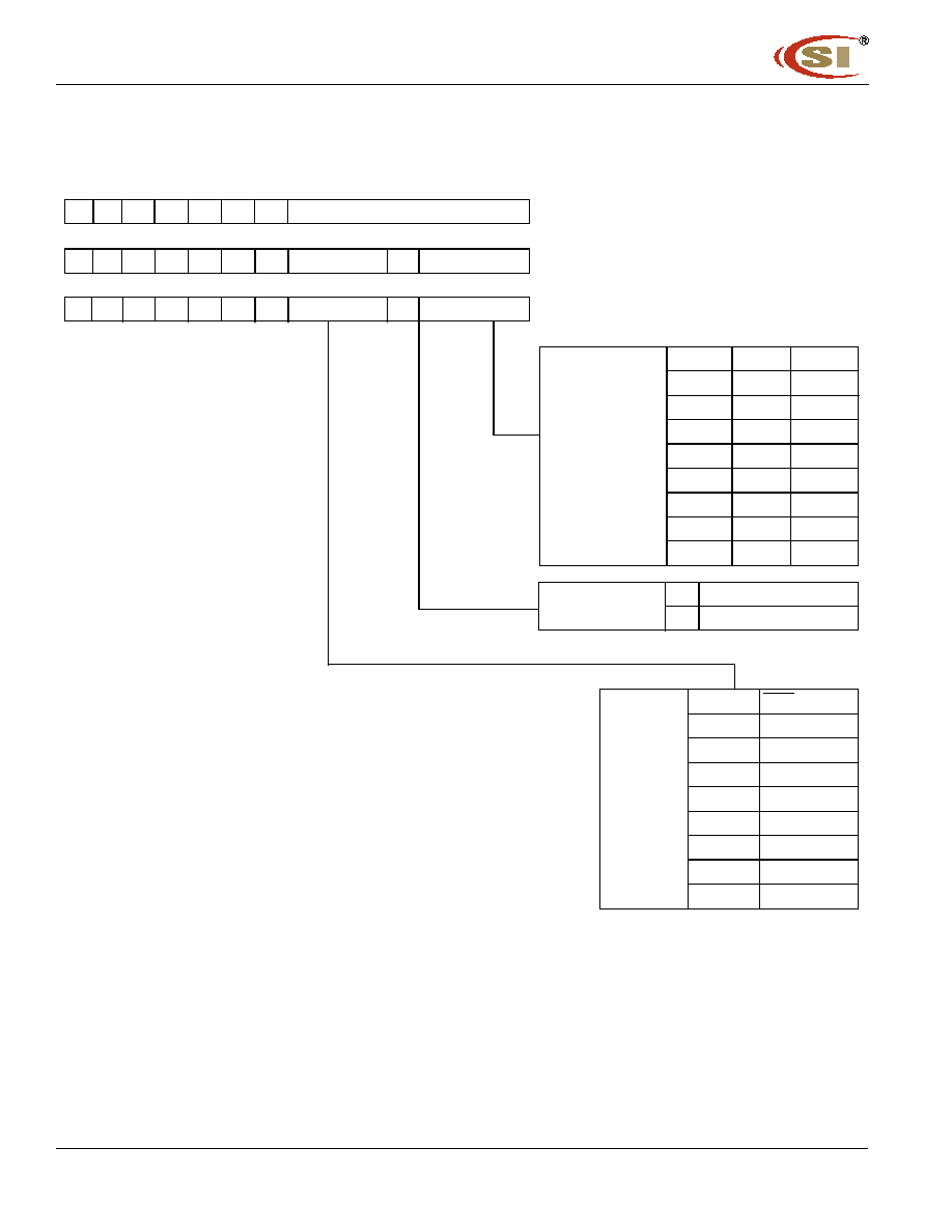
Programming the Mode Register
The mode register is programmed by the mode register
set command using address bits A13 through A0 as data
inputs. The register retains data until it is reprogrammed
or the device loses power.
The mode register has four fields;
Options : A13 through A7
CAS latency : A6 through A4
Wrap type : A3
Burst length : A2 through A0
Following mode register programming, no command can
be asserted befor at least two clock cycles have elapsed.
CAS
CAS
CAS
CAS
CAS Latency
CAS latency is the most critical parameter being set. It
tells the device how many clocks must elapse before the
data will be available.
The value is determined by the frequency of the clock and
the speed grade of the device. The value can be pro-
grammed as 2 or 3.
Burst Length
Burst Length is the number of words that will be output or
input in read or write cycle. After a read burst is completed,
the output bus will become high impedance.
The burst length is programmable as 1, 2, 4, 8 or full page.
Wrap Type (Burst Sequence)
The wrap type specifies the order in which the burst data
will be addressed. The order is programmable as either
"Sequential" or "Interleave". The method chosen will
depend on the type of CPU in the system.
IC42S16400
16
Integrated Circuit Solution Inc.
DR034-0E 12/02/2003
MODE REGISTER
0
0
0
0
1
13 12 11
10
9
8
5
4
3
2
1
0
JEDEC Standard Test Set
x
x
1
0
0
11
10
9
8
7
6
5
4
3
2
1
0
Burst Read and Single Write (for Write Through Cache)
LTMODE
WT
BL
0
0
0
0
0
11
10
9
8
7
6
5
4
3
2
1
0
Burst Read and Burst Write X = Don't care
LTMODE
WT
BL
Burst length
Bits2 - 0
WT = 1
WT = 0
000
001
010
011
100
101
110
111
1
2
4
8
R
R
R
Fullpage
1
2
4
8
R
R
R
R
Wrap type
0
1
Sequential
Interleave
Latency
Bits 6-4
CAS Iatency
000
001
010
011
100
101
110
111
R
R
2
3
R
R
R
R
mode
Remark R : Reserved
7
6
0
0
12
13
x
x
13 12
0
0

IC42S16400
Integrated Circuit Solution Inc.
17
DR034-0E 12/02/2003
Burst Length and Sequence
Burst of Two
Starting Address
Sequential Addressing
Interleave Addressing Sequence
(column address A0, binary)
Sequence (decimal)
(decimal)
0
0, 1
0, 1
1
1, 0
1, 0
Burst of Four
Starting Address
Sequential Addressing
Interleave Addressing Sequence
(column address A1 - A0, binary)
Sequence (decimal)
(decimal)
00
0, 1, 2, 3
0, 1, 2, 3
01
1, 2, 3, 0
1, 0, 3, 2
10
2, 3, 0, 1
2, 3, 0, 1
11
3, 0, 1, 2
3, 2, 1, 0
Burst of Eight
Starting Address
Sequential Addressing
Interleave Addressing Sequence
(column address A2 - A0, binary)
Sequence (decimal)
(decimal)
000
0, 1, 2, 3, 4, 5, 6, 7
0, 1, 2, 3, 4, 5, 6, 7
001
1, 2, 3, 4, 5, 6, 7, 0
1, 0, 3, 2, 5, 4, 7, 6
010
2, 3, 4, 5, 6, 7, 0, 1
2, 3, 0, 1, 6, 7, 4, 5
011
3, 4, 5, 6, 7, 0, 1 ,2
3, 2, 1, 0, 7, 6, 5, 4
100
4, 5, 6, 7, 0, 1, 2, 3
4, 5, 6, 7, 0, 1, 2, 3
101
5, 6 ,7, 0, 1, 2, 3, 4
5, 4, 7, 6, 1, 0, 3, 2
110
6, 7 ,0 ,1 ,2 ,3 ,4 ,5
6, 7, 4, 5, 2, 3, 0, 1
111
7, 0, 1, 2, 3, 4, 5, 6
7, 6, 5, 4, 3, 2, 1, 0
IC42S16400
18
Integrated Circuit Solution Inc.
DR034-0E 12/02/2003
Address Bits of Bank-Select and Precharge
A12
A13
Result
0
0
Select Bank A
"Activate " command
0
1
Select Bank B
"Activate" command
1
0
Select Bank C
"Activate" command
1
1
Select Bank D
"Activate" command
0
Disable Auto-Precharge (End of Burst)
1
Enable Auto - Precharge (End of Burst)
(Activate command)
A0 A1
A2
A3
A4
A5
A6
A7
A8
A9 A10 A11 A12 A13
A10
A12 A13 Result
0
0
0
Precharge Bank A
0
0
1
Precharge Bank B
0
1
0
Precharge Bank C
0
1
1
Precharge Bank D
1
X
X
Precharge All Banks
A12
A13
Result
0
0
Enable Read/Write
commands for Bank A
0
1
Enable Read/Write
commands for Bank B
1
0
Enable Read/Write
commands for Bank C
1
1
Enable Read/Write
commands for Bank D
Row
(Precharge command)
A0 A1 A2
A3
A4
A5
A6
A7
A8
A9 A10 A11 A12 A13
Row
(CAS strobes)
A0 A1
A2
A3
A4
A5
A6
A7
A8
A9 A10 A11 A12 A13
Co1.
X: Don't care

IC42S16400
Integrated Circuit Solution Inc.
19
DR034-0E 12/02/2003
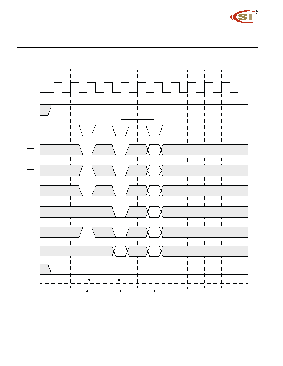
Precharge
The precharge command can be asserted anytime after t
RAS
(min.) is satisfied.
Soon after the precharge command is asserted, the precharge operation is performed and the synchronous DRAM enters
the idle state after t
RP
(min.) is satisfied. The parameter t
RP
is the time required to perform the precharge.
The earliest timing in a read cycle that a precharge command can be asserted without losing any data in the burst is as
follows.
PrechargeE
Burst lengh=4
CLK
Command
CAS latency = 2
DQ
Command
CAS latency = 3
DQ
(t
RAS
is satisfied)
Hi - Z
Q0
Q3
Q2
Q1
PRE
Q0
Q3
Q2
Q1
Read
Read
T0
T1
T2
T3
T4
T5
T6
T7
PRE
Hi - Z
In order to write all data to the memory cell correctly, the asynchronous parameter t
DPL
must be satisfied. The t
DPL
(min.)
specification defines the earliest time that a precharge command can be asserted. The minimum number of clocks can be
calculated by dividing t
DPL
(min.) with the clock cycle time.
In summary, the precharge command can be asserted relative to the reference clock that indicates the last data word is
valid. In the following table, minus means clocks before the reference; plus means time after the reference.
CAS
CAS
CAS
CAS
CAS latency
Read
Write
2
-1
+ t
DPL
((min.)
3
-2
+ t
DPL
((min.)

IC42S16400
20
Integrated Circuit Solution Inc.
DR034-0E 12/02/2003
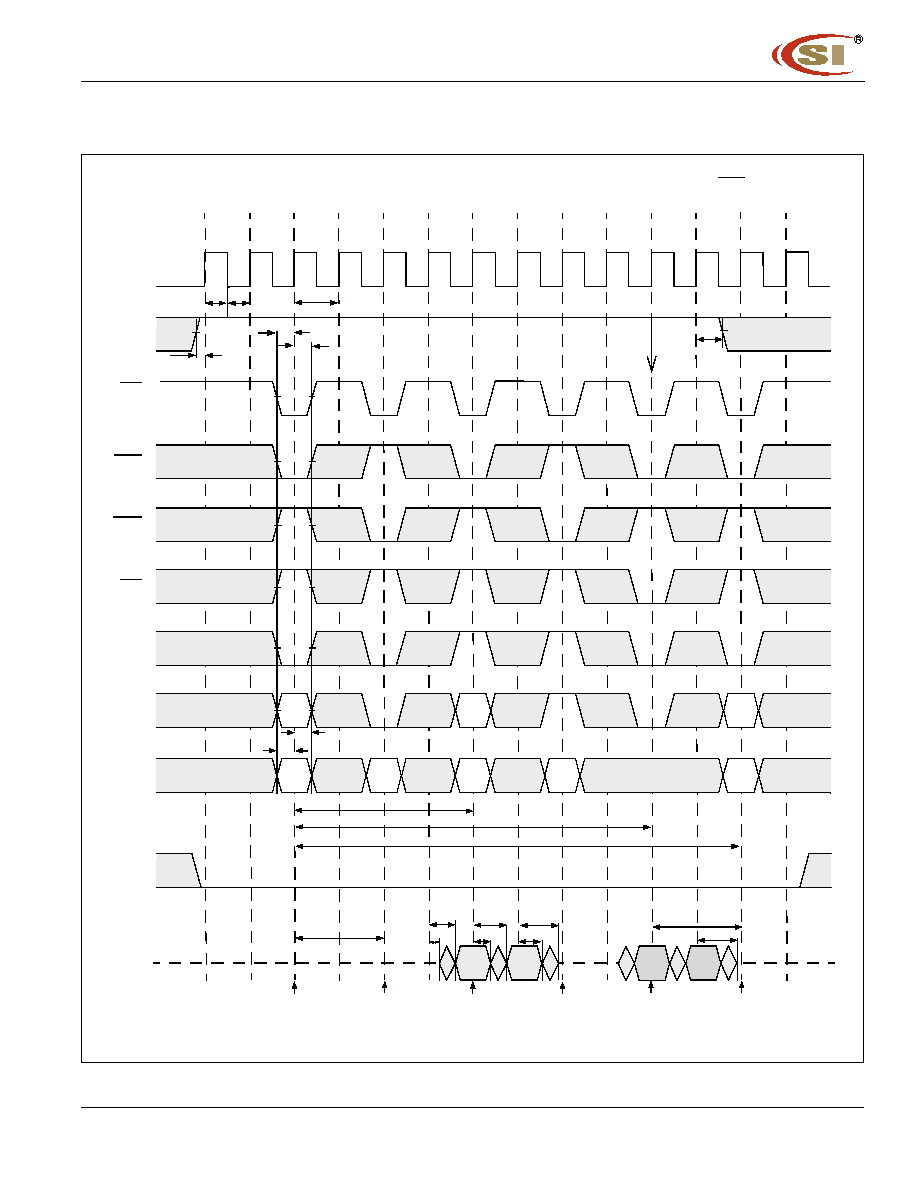
Auto Precharge
During a read or write command cycle, A10 controls whether auto precharge is selected. If A10 is high in the read or write
command (Read with Auto precharge command or Write with Auto precharge command), auto precharge is selected and
begins automatically.
In the write cycle, t
DAL
(min.) must be satisfied before asserting the next activate command to the bank being precharged.
When using auto precharge in the read cycle, knowing when the precharge starts is important because the next activate
command to the bank being precharged cannot be executed until the precharge cycle ends. Once auto precharge has
started, an activate command to the bank can be asserted after t
RP
has been satisfied.
A Read or Write command without auto - precharge can be terminated in the midst of a burst operation. However, a Read
or Write command with auto - precharge can not be interrupted by the same bank commands before the entire burst opera-
tion is completed. Therefore use of the same bank Read, Write, Precharge or Burst Stop command is prohibited during a
read or write cycle with auto - precharge. It should be noted that the device will not respond to the Auto - Precharge com-
mand if the device is programmed for full page burst read or write cycles.
The timing when the auto precharge cycle begins depends both on both the CAS Iatency programmed into the mode reg-
ister and whether the cycle is read or write.
Read with Auto Precharge
During a READA cycle, the auto precharge begins one clock earlier (CL = 2) or two clocks earlier (CL = 3) than the last word
output.
READ with AUTO PRECHARGE
Burst lengh = 4
CLK
Command
CAS latency = 2
DQ
Command
CAS latency = 3
DQ
Remark READA means READ with AUTO PRECHARGE
Hi - Z
Auto precharge starts
QB0
QB3
QB2
QB1
READA B
READA B
T0
T1
T2
T3
T4
T5
T6
T7
Auto precharge starts
Hi - Z
T8
QB0
QB3
QB2
QB1
No New Command to Bank B
No New Command to Bank B

IC42S16400
Integrated Circuit Solution Inc.
21
DR034-0E 12/02/2003
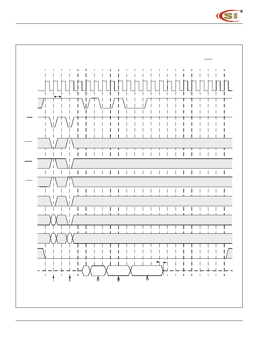
Write with Auto Precharge
During a write cycle, the auto precharge starts at the timing that is equal to the value of t
DPL
(min.) after the last data word
input to the device.
In summary, the auto precharge cycle begins relative to a reference clock that indicates the last data word is valid. In the
table below, minus means clocks before the reference; plus means clocks after the reference.
CAS
CAS
CAS
CAS
CAS latency
Read
Write
2
-1
+ t
DPL
((min.)
3
-2
+ t
DPL
((min.)
WRITE with AUTO PRECHRGE
Burst lengh = 4
CLK
Command
CAS latency = 2
DQ
Command
CAS latency = 3
DQ
Remark WRITA means WRITE with AUTO Precharge
Hi - Z
DB0
DB3
DB2
DB1
WRITA B
WRITA B
T0
T1
T
2
T3
T4
T5
T6
T7
Hi - Z_
T8
t
DPL
t
DPL
DB0
DB3
DB2
DB1
AUTO PRECHARGE starts
AUTO PRECHARGE starts
IC42S16400
22
Integrated Circuit Solution Inc.
DR034-0E 12/02/2003
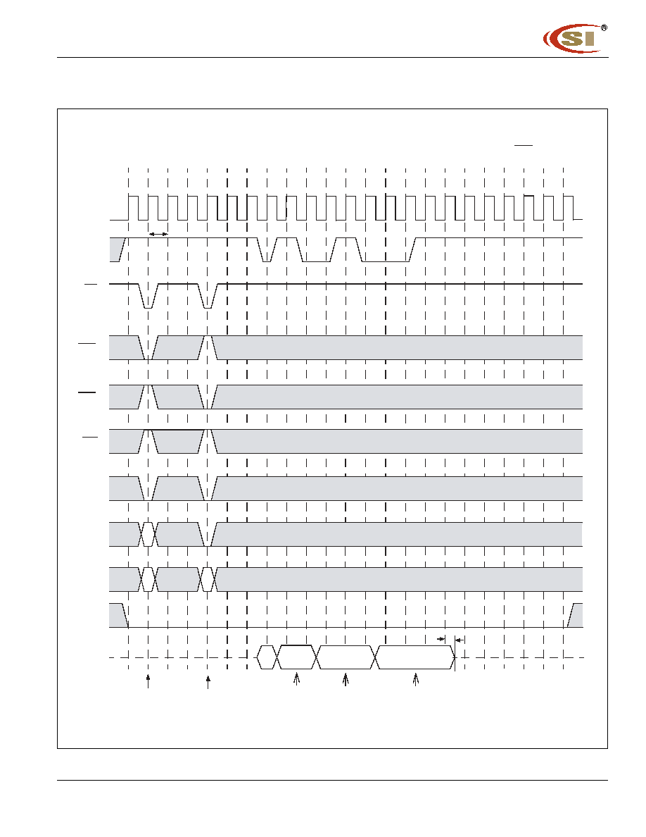
Read / Write Command Interval
Read to Read Command Interval
During a read cycle when a new read command is asserted, it will be effective after the CAS latency, even if the previous
read operation has not completed. READ will be interrupted by another READ.
Each read command can be asserted in every clock without any restriction.
Write to Write Command Interval
During a write cycle, when a new Write command is asserted, the previous burst will terminate and the new burst will begin
with a new write command. WRITE will be interrupted by another WRITE.
Each write command can be asserted in every clock without any restriction.
READ to READ Command Interval
Burst lengh=4, CAS latency=2
CLK
Command
DQ
QA0
QB2
QB1
QB0
Read A
T0
T1
T2
T3
T4
T5
T6
T7
Hi-Z_
T8
1 cycle
QB3
Read B
Burst lengh=4, CAS latency=2
CLK
Command
DQ
QA0
QB2
QB1
QB0
Write A
T0
T1
T2
T3
T4
T5
T6
T7
Hi-Z_
T8
1 cycle
QB3
Write B
WRITE to WRITE Command Interval

IC42S16400
Integrated Circuit Solution Inc.
23
DR034-0E 12/02/2003
Write to Read Command Interval
The write command to read command interval is also a minimum of 1 cycle. Only the write data before the read command
will be written. The data bus must be Hi-Z at least one cycle prior to the first D
OUT
.
WRITE to READ Command Interval
Burst lengh=4
CLK
Command
CAS latency=2
DQ
Command
CAS latency=3
DQ
QB0
QB3
QB2
QB1
WRITE A
Write A
T0
T1
T2
T3
T4
T5
T6
T7
T8
QB0
QB3
QB2
QB1
1 cycle
Read B
DA0
Read B
DA0
Hi-Z
Hi-Z
Read to Write Command Interval
During a read cycle, READ can be interrupted by WRITE.
DQM must be in High at least 3 clocks prior to the write command. There is a restriction to avoid a data conflict. The data
bus must be Hi-Z using DQM before Write.
IC42S16400
24
Integrated Circuit Solution Inc.
DR034-0E 12/02/2003
READ to WRITE Command Interval
CAS latency=2
CLK
Command
DQM
DQ
Hi-Z
D0
D3
D2
D1
Read
T0
T1
T2
T3
T4
T5
T6
T7
T8
1 cycle
Write
Burst length=8, CAS latency=2
CLK
Command
DQM
DQ
Q0
Read
T0
T1
T2
T3
T4
T5
T6
T7
T8
Write
T9
necessary
Q2
Q1
D0
D2
D1
Hi-Z is
example: Burst length=4, CAS latency=3
CLK
Command
DQM
DQ
Read
T0
T1
T2
T3
T4
T5
T6
T7
T8
Write
necessary
D0
D2
D1
Hi-Z is
Q2

IC42S16400
Integrated Circuit Solution Inc.
25
DR034-0E 12/02/2003
BURST Termination
There are two methods to terminate a burst operation other than using a read or a write command. One is the burst stop
command and the other is the precharge command.
BURST Stop Command
During a read burst, when the burst stop command is issued, the burst read data are terminated and the data bus goes to
high-impedance after the CAS latency from the burst stop command.
During a write burst, when the burst stop command is issued, the burst write data are termained and data bus goes to Hi-
Z at the same clock with the burst stop command.
Burst Termination
Burst lengh=X, CAS Intency=2,3
CLK
Command
CAS latency=2
DQ
CAS latency=3
DQ
Q0
Q2
Q1
Read
T0
T1
T2
T3
T4
T5
T6
T7
BST
Hi-Z
Q0
Q2
Q1
Hi-Z
Remark BST: Burst stop command
Remark BST: Burst command
Burst lengh=X, CAS latency=2,3
CLK
Command
CAS latency=2,3
DQ
Q0
Q2
Q1
Write
T0
T1
T2
T3
T4
T5
T6
T7
BST
Hi-Z_
Q0

IC42S16400
26
Integrated Circuit Solution Inc.
DR034-0E 12/02/2003
PRECHARGE TERMINATION
PRECHARGE TERMINATION in READ Cycle
During READ cycle, the burst read operation is terminated by a precharge command.
When the precharge command is issued, the burst read operation is terminated and precharge starts.
The same bank can be activated again after t
RP
from the precharge command.
When CAS latency is 2, the read data will remain valid until one clock after the precharge command.
When CAS latency is 3, the read data will remain valid until two clocks after the precharge command.
Precharge Termination in READ Cycle
Burst lengh= X
CLK
Command
CAS latency=2
DQ
Hi-Z
Read
T0
T1
T2
T3
T4
T5
T6
T7
T8
PRE
ACT
DQ
Read
PRE
ACT
t
RP
CAS latency=3
Q0
Q3
Q2
Q1
Hi-Z
Q0
Q3
Q2
Q1
command
t
RP
IC42S16400
Integrated Circuit Solution Inc.
27
DR034-0E 12/02/2003
Precharge Termination in WRITE Cycle
During WRITE cycle, the burst write operation is terminated by a precharge command.
When the precharge command is issued, the burst write operation is terminated and precharge starts.
The same bank can be activated again after t
RP
from the precharge command. The DQM must be high to mask
invalid data in.
During WRITE cycle, the write data written prior to the precharge command will be correctly stored. However, invalid
data may be written at the same clock as the precharge command. To prevent this from happening, DQM must be high
at the same clock as the precharge command. This will mask the invalid data.
PRECHARGE TERMINATION in WRITE Cycle
Burst lengh = X
CLK
Command
CAS latency = 2
DQM
Hi - Z
Write
T0
T1
T2
T3
T4
T5
T6
T7
T8
t
RP
PRE
ACT
DQ
Write
PRE
ACT
t
RP
CAS latency = 3
Hi - Z
D0
D3
D2
D1
D0
D3
D2
D1
DQM
D4
D4
command
DQ
IC42S16400
28
Integrated Circuit Solution Inc.
DR034-0E 12/02/2003
T0 T1 T2 T3 T4 T5 T6 T7 T8 T9 T10
CLK
CKE
CS
RAS
CAS
WE
BS0,1
A10
ADD
DQM
DQ
Command
Mode Register
Set
Command
All Banks
Precharge
Command
t
RP
t
RSC
Hi-Z
Address Key
Mode Register Set

IC42S16400
Integrated Circuit Solution Inc.
29
DR034-0E 12/02/2003
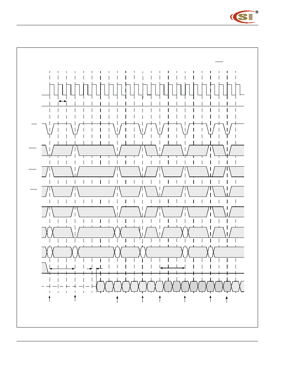
AC Parameters for Write Timing (1 of 2)
BS1="L", Bank C,D = Idle
T0 T1 T2 T3 T4 T5 T6 T7 T8 T9 T10 T11 T12 T13 T14 T15 T16 T17 T18 T19 T20 T21 T22
t
CH
t
CL
t
CKS
t
CMS
t
CMH
tAS
t
AH
Begin Auto Precharge
Bank A
Begin Auto Precharge
Bank B
t
CKH
t
CK2
CLK
CKE
CS
RAS
CAS
WE
*BS0
A10
ADD
DQM
DQ
tRCD
t
RRD
t
RC
t
DAL
QAa0 QAa1 QAa2 QAa3 QBa0 QBa1 QBa2 QBa3 QAb0 QAb1 QAb2 QAb3
Activate
Command
Bank A
Write with
Auto Precharge
Command
Bank A
Activate
Command
Bank B
Write with
Auto Precharge
Command
Bank B
Activate
Command
Bank A
Write without
Auto Precharge
Command
Bank A
t
DS
t
DH
t
DPL
RP
t
Precharge
Command
Bank A
Activate
Command
Bank A
Burst Length=4, CAS Latency=3
Activate
Command
Bank B

IC42S16400
30
Integrated Circuit Solution Inc.
DR034-0E 12/02/2003
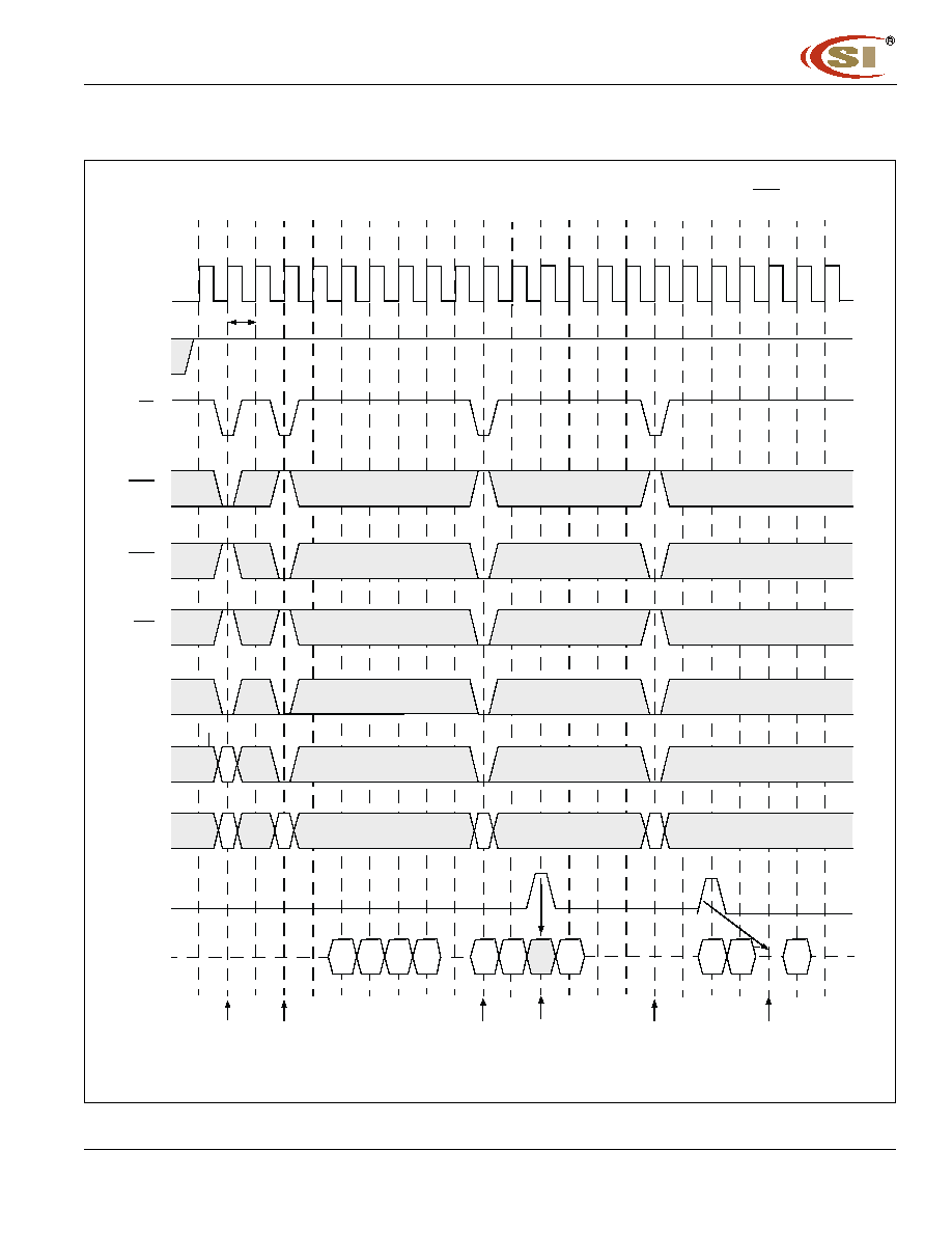
AC Parameters for Write Timing (2 of 2)
BS1="L", Bank C,D = Idle
T0 T1 T2 T3 T4 T5 T6 T7 T8 T9 T10 T11 T12 T13 T14 T15 T16 T17 T18 T19 T20 T21 T22 T23
t
CH
t
CL
t
CKS
t
CMS
t
CMH
tAS
tAH
Begin Auto Precharge
Bank A
Begin Auto Precharge
Bank B
t
CKH
t
CK3
CLK
CKE
CS
RAS
CAS
WE
A10
ADD
DQM
DQ
tRCD
t
RRD
RC
t
DAL
QAa0 QAa1 QAa2 QAa3 QBa0 QBa1 QBa2 QBa3
QAb0 QAb1 QAb2 QAb3
Activate
Command
Bank A
Write with
Auto Precharge
Command
Bank A
Activate
Command
Bank B
Write with
Auto Precharge
Command
Bank B
Activate
Command
Bank A
Write without
Auto Precharge
Command
Bank A
t
DS
t
DH
t
DPL
RP
t
Precharge
Command
Bank A
Activate
Command
Bank A
Burst Length=4, CAS Latency=3
*BS0
IC42S16400
Integrated Circuit Solution Inc.
31
DR034-0E 12/02/2003
AC Parameters for Read Timing (1 of 2)
BS1="L", Bank C,D = Idle
T0 T1 T2 T3 T4 T5 T6 T7 T8 T9 T10 T11 T12 T13
CLK
CKE
CS
RAS
CAS
WE
A10
ADD
DQM
DQ
Burst Length=2, CAS Latency=2
tCH tCL
tCK2
Begin Auto
Precharge
Bank B
t
CKH
tCKS
tCMS
t
CMH
tAH
tAS
tRRD
tRAS
tRC
t
RCD
t
AC2
tLZ
tOH
t
AC2
tOH
tHZ
tRP
tHZ
Hi-Z
Activate
Command
Bank A
Read
Command
Bank A
Activate
Command
Bank B
Read with
Auto Precharge
Bank B
Precharge
Command
Bank A
Activate
Command
Bank A
QAa0
QAa1
QBa0
QBa1
Command
*BS0

IC42S16400
32
Integrated Circuit Solution Inc.
DR034-0E 12/02/2003
AC Parameters for Read Timing (2 of 2)
BS1="L", Bank C,D = Idle
T0 T1 T2 T3 T4 T5 T6 T7 T8 T9 T10 T11 T12 T13 T14 T15
CLK
CKE
CS
RAS
CAS
WE
A10
ADD
DQM
DQ
Burst Length=2, CAS Latency=3
tLZ
t
HZ
Hi-Z
Activate
Command
Bank A
Read
Command
Bank A
Activate
Command
Bank B
Read with
Auto Precharge
Bank B
Precharge
Command
Bank A
Activate
Command
Bank A
t
CH tCL
t
CKS
t
CK3
t
CMS
t
CMH
t
AH
t
AS
t
RRD
t
RAS
t
RC
t
RP
t
RCD
tAC3
tOH
tAC3
QAa0
QAa1
QBa0
QBa1
tOH
tHZ
Command
t
CKH
Begin Auto
Precharge
Bank B
*BS0

IC42S16400
Integrated Circuit Solution Inc.
33
DR034-0E 12/02/2003
Power on Sequence and Auto Refresh (CBR)
T0 T1 T2 T3 T4 T5 T6 T7 T8 T9 T10 T11 T12 T13 T14 T15 T16 T17 T18 T19 T20 T21 T22
CLK
CKE
CS
RAS
CAS
WE
A10
ADD
DQM
DQ
High level
is required
Minimum of 8 Refresh Cycles are required
t
RSC
t
RP
High Level is Necessary
t
RC
Address Key
Inputs
be stable
for 200us
Precharge
All Banks
must
Command
1st Auto
Command
Refresh
2nd Auto
Refresh
Command
Mode
Set Command
Command
Register
Hi-Z
BS0, 1
IC42S16400
34
Integrated Circuit Solution Inc.
DR034-0E 12/02/2003
Clock Suspension During Burst Read (Using CKE) (1 of 2)
BS1="L", Bank C,D = Idle
T0 T1 T2 T3 T4 T5 T6 T7 T8 T9 T10 T11 T12 T13 T14 T15 T16 T17 T18 T19 T20 T21 T22
CLK
CKE
CS
RAS
CAS
WE
A10
ADD
DQM
DQ
t
HZ
Activate
Bank A
Command
Read
Bank A
Command
Clock
2 Cycles
Hi-Z
QAa0
QAa1
QAa2
QAa3
RAa
CAa
RAa
t
CK2
Clock
Suspended
1 Cycle
Suspended
Clock
3 Cycles
Suspended
Burst Length=4, CAS Latency=2
*BS0
IC42S16400
Integrated Circuit Solution Inc.
35
DR034-0E 12/02/2003
Clock Suspension During Burst Read (Using CKE) (2 of 2)
BS1="L", Bank C,D = Idle
T0 T1 T2 T3 T4 T5 T6 T7 T8 T9 T10 T11 T12 T13 T14 T15 T16 T17 T18 T19 T20 T21 T22
CLK
CKE
CS
RAS
CAS
WE
A10
ADD
DQM
DQ
t
HZ
Activate
Bank A
Command
Read
Bank A
Command
Clock
2 Cycles
Hi-Z
QAa0
QAa1
QAa2
QAa3
RAa
RAa
t
CK3
Clock
Suspended
1 Cycle
Suspended
Clock
3 Cycles
Suspended
Burst Length=4, CAS Latency=3
CAa
*BS0

IC42S16400
36
Integrated Circuit Solution Inc.
DR034-0E 12/02/2003
Clock Suspension During Burst Write (Using CKE) (1 of 2)
BS1="L", Bank C,D = Idle
T0 T1 T2 T3 T4 T5 T6 T7 T8 T9 T10 T11 T12 T13 T14 T15 T16 T17 T18 T19 T20 T21 T22
CLK
CKE
CS
RAS
CAS
WE
A10
ADD
DQM
DQ
Activate
Bank A
Command
Write
Bank A
Command
Clock
2 Cycles
Hi-Z
RAa
CAa
RAa
t
CK2
Clock
Suspended
1 Cycle
Suspended
Clock
3 Cycles
Suspended
Burst Length=4, CAS Latency=2
DAa0
DAa1
DAa2
DAa3
*BS0

IC42S16400
Integrated Circuit Solution Inc.
37
DR034-0E 12/02/2003
Clock Suspension During Burst Write (Using CKE) (2 of 2)
BS1="L", Bank C,D = Idle
T0 T1 T2 T3 T4 T5 T6 T7 T8 T9 T10 T11 T12 T13 T14 T15 T16 T17 T18 T19 T20 T21 T22
CLK
CKE
CS
RAS
CAS
WE
A10
ADD
DQM
DQ
RAa
RAa
t
CK3
Burst Length=4, CAS Latency=3
CAa
Activate
Bank A
Command
Write
Bank A
Command
Clock
2 Cycles
Hi-Z
Clock
Suspended
1 Cycle
Suspended
Clock
3 Cycles
Suspended
DAa0
DAa1
DAa2
DAa3
*BS0

IC42S16400
38
Integrated Circuit Solution Inc.
DR034-0E 12/02/2003
Power Down Mode and Clock Mask
BS1="L", Bank C,D = Idle
T0 T1 T2 T3 T4 T5 T6 T7 T8 T9 T10 T11 T12 T13 T14 T15 T16 T17 T18 T19 T20 T21 T22
CLK
CKE
CS
RAS
CAS
WE
A10
ADD
DQM
DQ
RAa
RAa
t
CK2
Burst Length=4, CAS Latency=2
Activate
Bank A
Command
Power Down
Mode Entry
Power Down
Bank A
Hi-Z
ACTIVE
STANDBY
Read
Clock Mask
CAa
t
CKS
t
CKH
VALID
t
CKS
RAa
QAa0 QAa1
QAa2
Mode Exit
Command
Start
Clock Mask
End
Precharge
Command
Power Down
Mode Entry
Precharge
Standby
Power
Mode
Down
Exit
Command
*BS0
QAa3
IC42S16400
Integrated Circuit Solution Inc.
39
DR034-0E 12/02/2003
Auto Refresh (CBR)
BS1="L", Bank C,D = Idle
T0 T1 T2 T3 T4 T5 T6 T7 T8 T9 T10 T11 T12 T13 T14 T15 T16 T17 T18 T19 T20 T21 T22
CLK
CKE
CS
RAS
CAS
WE
A10
ADD
DQM
DQ
t
CK2
Burst Length=4, CAS Latency=2
Precharge
All Banks
Command
CBR Refresh
Hi-Z
CBR Refresh
Command
Activate
Command
Read
RAa
CAa
RAa
Q0
Q1
Q2
Q3
Command
Command
t
RP
t
RC
t
RC
*BS0, 1

IC42S16400
40
Integrated Circuit Solution Inc.
DR034-0E 12/02/2003
Self Refresh (Entry and Exit)
BS1="L", Bank C,D = Idle
Clock can be stopped at CKE=Low. If clock is stopped, it must be restarted/stable for 4 clock cycles before CKE=High
T0 T1 T2 T3 T4 T5 T6 T7 T8 T9 T10 T11 T12 T13 T14 T15 T16 T17 T18 T19 T20 T21 T22
CLK
CKE
CS
RAS
CAS
WE
A10
ADD
DQM
DQ
t
SRX
All Banks
Self refresh
Hi-Z
Self Refresh
Exit
Self Refresh
Entry
Exit
t
RC
t
CKS
t
SRX
t
CKS
t
RC
must be idle
Self Refresh
Entry
Activate
Command
CLK can be Stopped
**
*BS0
IC42S16400
Integrated Circuit Solution Inc.
41
DR034-0E 12/02/2003
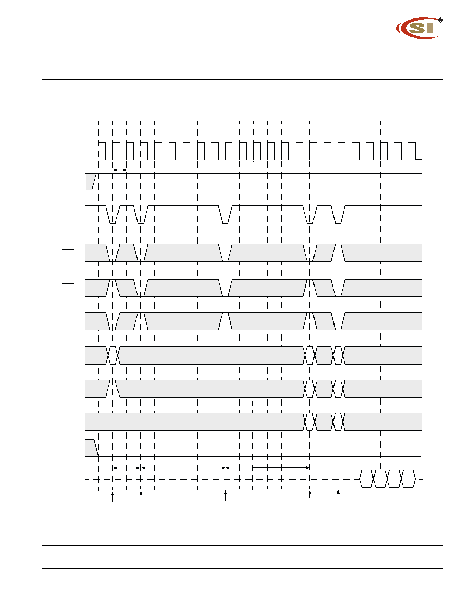
Random Column Read (Page With Same Bank) (1 of 2)
BS1="L", Bank C,D = Idle
T0 T1 T2 T3 T4 T5 T6 T7 T8 T9 T10 T11 T12 T13 T14 T15 T16 T17 T18 T19 T20 T21 T22
CLK
CKE
CS
RAS
CAS
WE
A10
ADD
DQM
DQ
t
CK2
Burst Length=4, CAS Latency=2
Precharge
Bank A
Command
Read
Hi-Z
Activate
Read
RAa
QAd0
Command
Command
RAa
CAa
RAa
CAb CAc
RAd
RAd
CAd
QAa0 QAa1 QAa2 QAa3 QAb0 QAb1 QAc0 QAc1 QAc2 QAc3
QAd1 QAd2 QAd3
Bank A
Read
Command
Bank A
Read
Command
Bank A
Precharge
Command
Bank A
Bank A
Command
Bank A
*BS0
IC42S16400
42
Integrated Circuit Solution Inc.
DR034-0E 12/02/2003
Random Column Read (Page With Same Bank) (2 of 2)
BS1="L", Bank C,D = Idle
T0 T1 T2 T3 T4 T5 T6 T7 T8 T9 T10 T11 T12 T13 T14 T15 T16 T17 T18 T19 T20 T21 T22
CLK
CKE
CS
RAS
CAS
WE
A10
ADD
DQM
DQ
t
CK3
Burst Length=4, CAS Latency=3
Activate
Bank A
Command
Read
Hi-Z
Activate
Read
Command
Command
RAa
CAa
CAb CAc
RAd
CAd
QAc2 QAc3
QAa0 QAa1 QAa2 QAa3 QAb0 QAb1 QAc0 QAc1
Bank A
Read
Command
Bank A
Precharge
Command
Bank A
Bank A
Command
Bank A
RAd
Read
Command
Bank A
RAa
*BS0

IC42S16400
Integrated Circuit Solution Inc.
43
DR034-0E 12/02/2003
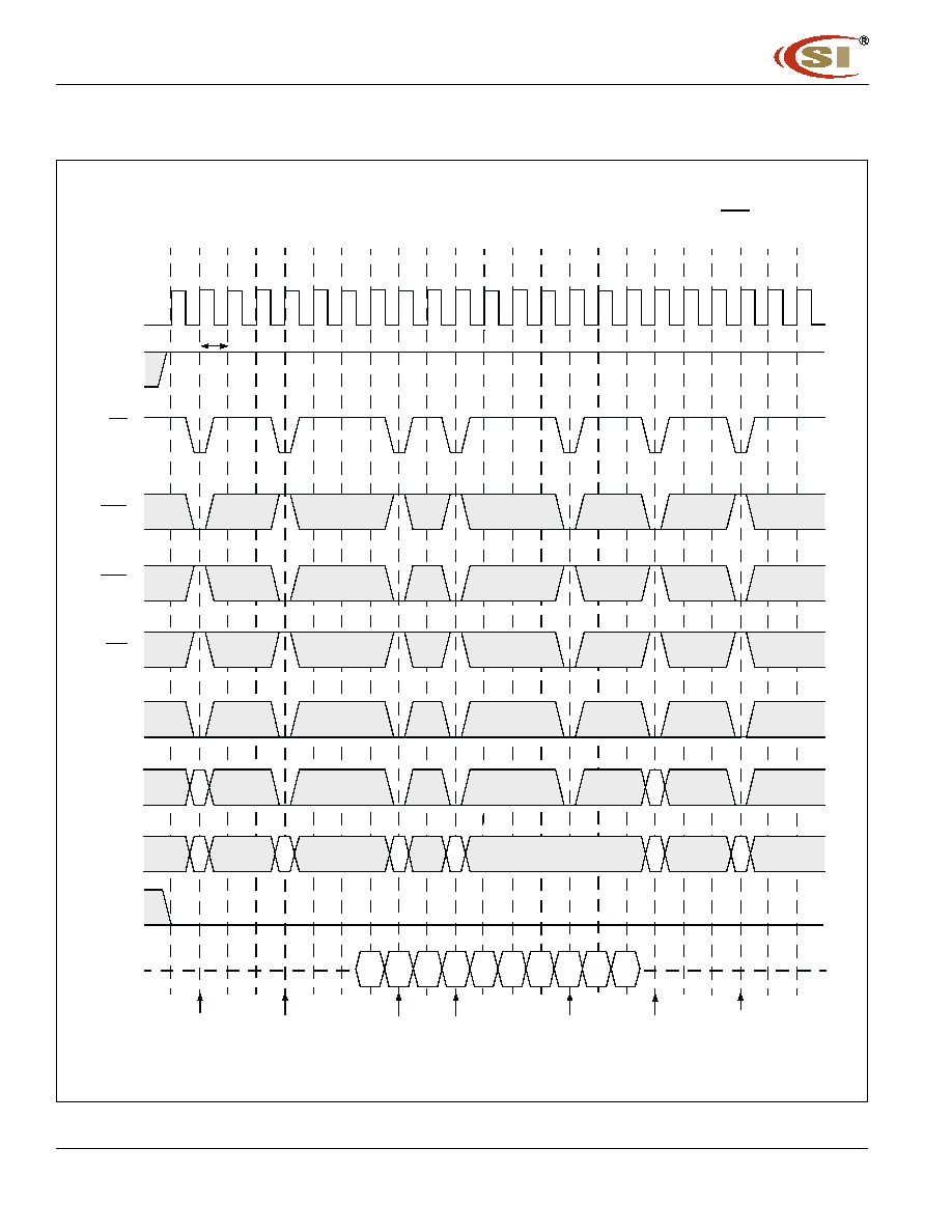
Random Column Write (Page With Same Bank) (1 of 2)
BS1="L", Bank C,D = Idle
T0 T1 T2 T3 T4 T5 T6 T7 T8 T9 T10 T11 T12 T13 T14 T15 T16 T17 T18 T19 T20 T21 T22
CLK
CKE
CS
RAS
CAS
WE
A10
ADD
DQM
DQ
t
CK2
Burst Length=4, CAS Latency=2
Activate
Bank B
Command
Write
Hi-Z
Activate
Write
Command
Command
Ra
Ca
Ra
Cb
Cc
Rd
Cd
Dc2
Dc3
Da1
Da2
Da3
Db0
Db1 Dc0 Dc1
Bank B
Write
Command
Bank B
Precharge
Command
Bank B
Bank B
Command
Bank B
Write
Command
Bank B
Rd
Dd2
Dd3
Dd0 Dd1
Da0
*BS0

IC42S16400
44
Integrated Circuit Solution Inc.
DR034-0E 12/02/2003
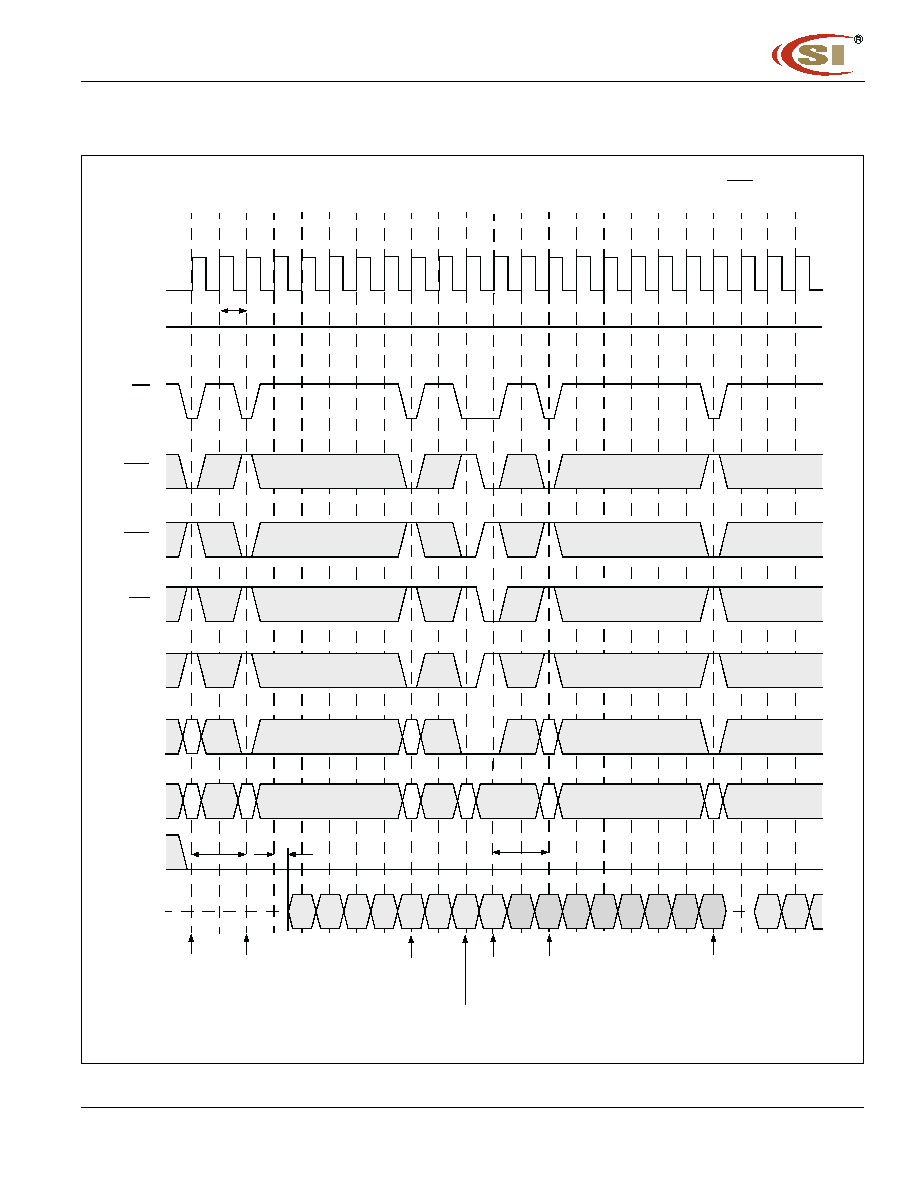
Random Column Write (Page With Same Bank) (1 of 2)
BS1="L", Bank C,D = Idle
T0 T1 T2 T3 T4 T5 T6 T7 T8 T9 T10 T11 T12 T13 T14 T15 T16 T17 T18 T19 T20 T21 T22
CLK
CKE
CS
RAS
CAS
WE
A10
ADD
DQM
DQ
t
CK
Burst Length=4, CAS Latency=3
Activate
Bank B
Command
Write
Hi-Z
Activate
Command
Ra
Ca
Ra
Cb
Cc
Cd
Rd
Bank B
Write
Command
Bank B
Precharge
Command
Bank B
Command
Bank B
Write
Command
Bank B
Rd
Write
Command
Bank B
Dc2
Dc3
Da1
Da2
Da3
Db0
Db1
Dc0
Dc1
Da0
Dd0
Dd1
*BS0
IC42S16400
Integrated Circuit Solution Inc.
45
DR034-0E 12/02/2003
Random Row Read (Interleaving Banks) (1 of 2)
BS1="L", Bank C,D = Idle
T0 T1 T2 T3 T4 T5 T6 T7 T8 T9 T10 T11 T12 T13 T14 T15 T16 T17 T18 T19 T20 T21 T22
CLK
CKE
CS
RAS
CAS
WE
A10
ADD
DQM
DQ
t
CK2
Burst Length=8, CAS Latency=2
Activate
Bank B
Command
Read
Hi-Z
Command
QAa0 QAa1
QBa1 QBa2 QBa3 QBa4 QBa5 QBa6 QBa7
Bank B
Activate
Command
Bank A
Active
Command
Bank B
Read
Command
Bank A
QBb1
QBb0
QBa0
Read
Command
Bank B
QAa3 QAa4 QAa5 QAa6 QAa7
QAa2
Precharge
Command
Bank B
t
RCD
t
AC2
t
RP
High
*BS0
IC42S16400
46
Integrated Circuit Solution Inc.
DR034-0E 12/02/2003
Random Row Read (Interleaving Banks) (2 of 2)
BS1="L", Bank C,D = Idle
T0 T1 T2 T3 T4 T5 T6 T7 T8 T9 T10 T11 T12 T13 T14 T15 T16 T17 T18 T19 T20 T21 T22
CLK
CKE
CS
RAS
CAS
WE
A10
ADD
DQM
DQ
t
CK3
Burs tLength=8, CAS Latency=3
Activate
Bank B
Command
Read
Hi-Z
Command
QAa0 QAa1
QBa1 QBa2 QBa3 QBa4 QBa5 QBa6 QBa7
Bank B
Activate
Command
Bank A
Precharge
Command
Bank B
QBb0
QBa0
Read
Command
Bank B
QAa3 QAa4 QAa5 QAa6 QAa7
QAa2
Read
Command
Bank A
t
RCD
t
AC3
t
RP
High
Activate
Bank B
Command
Precharge
Command
Bank A
*BS0

IC42S16400
Integrated Circuit Solution Inc.
47
DR034-0E 12/02/2003
Random Row Write (Interleaving Banks) (1 of 2)
BS1="L", Bank C,D = Idle
T0 T1 T2 T3 T4 T5 T6 T7 T8 T9 T10 T11 T12 T13 T14 T15 T16 T17 T18 T19 T20 T21 T22
CLK
CKE
CS
RAS
CAS
WE
A10
ADD
DQM
DQ
t
CK2
Burst Length=8, CAS Latency=2
Activate
Bank A
Command
Write
Hi-Z
Command
QBa0 QBa1
QAa1 QAa2 QAa3 QAa4 QAa5 QAa6 QAa7
Bank A
Activate
Command
Bank B
Active
Command
Bank A
Write
Command
Bank B
QAb3
QAb2
QAa0
Write
Command
Bank A
QBa3 QBa4 QBa5 QBa6 QBa7
QBa2
Precharge
Command
Bank A
t
RCD
t
RP
High
t
DPL
QAb0 QAb1
QAb4
Precharge
Command
Bank B
*BS0

IC42S16400
48
Integrated Circuit Solution Inc.
DR034-0E 12/02/2003
Random Row Write (Interleaving Banks) (2 of 2)
BS1="L", Bank C,D = Idle
T0 T1 T2 T3 T4 T5 T6 T7 T8 T9 T10 T11 T12 T13 T14 T15 T16 T17 T18 T19 T20 T21 T22
CLK
CKE
CS
RAS
CAS
WE
A10
ADD
DQM
DQ
t
CK
Burst Length=8, CAS Latency=3
Activate
Bank A
Command
Write
Hi-Z
Command
QAa7 QBa0
QAa0 QAa1 QAa2 QAa3 QAa4 QAa5 QAa6
Bank A
Activate
Command
Bank B
QAb2
QAb1
Activate
Command
Bank A
QBa2 QBa3 QBa4 QBa5 QBa6
QBa1
Write
Command
Bank B
RBa
t
RP
High
t
DPL
t
DPL
QBb7 QAb0
QAb3
Write
Command
Bank A
Precharge
Command
Bank A
Precharge
Command
Bank B
*BS0
IC42S16400
Integrated Circuit Solution Inc.
49
DR034-0E 12/02/2003
Read and Write Cycle (1 of 2)
BS1="L", Bank C,D = Idle
T0 T1 T2 T3 T4 T5 T6 T7 T8 T9 T10 T11 T12 T13 T14 T15 T16 T17 T18 T19 T20 T21 T22
CLK
CKE
CS
RAS
CAS
WE
A10
ADD
DQM
DQ
t
CK2
Burst Length=4, CAS Latency=2
Activate
Bank A
Command
Write
Hi-Z
Command
DAb3
QAc0
QAa0 QAa1 QAa2 QAa3
DAb0 DAb1
Bank A
Write
Command
Bank A
Read
Command
Bank A
QAc3
QAc1
The Read Data
The Write Data
is Masked with a
Zero Clock
RAa
RAa
CAb
CAc
CAa
latency
is Masked with
Two Clocks
Latency
*BS0
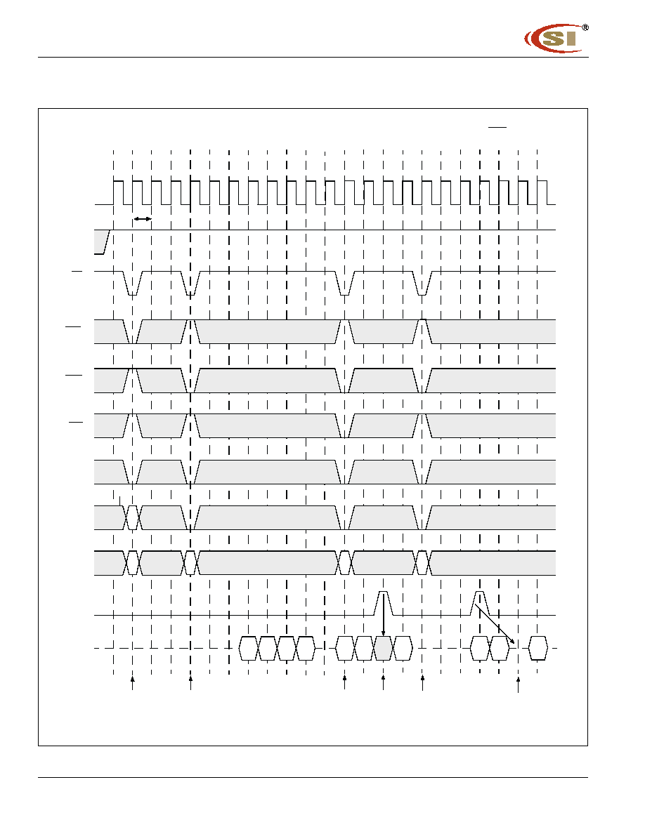
IC42S16400
50
Integrated Circuit Solution Inc.
DR034-0E 12/02/2003
Read and Write Cycle (2 of 2)
BS1="L", Bank C,D = Idle
T0 T1 T2 T3 T4 T5 T6 T7 T8 T9 T10 T11 T12 T13 T14 T15 T16 T17 T18 T19 T20 T21 T22
CLK
CKE
CS
RAS
CAS
WE
A10
ADD
DQM
DQ
t
CK3
Burst Length=4, CAS Latency=3
Activate
Bank A
Command
Read
Hi-Z
Command
DAb3
QAc0
QAa0 QAa1 QAa2 QAa3
DAb0 DAb1
Bank A
Write
Command
Bank A
QAc3
QAc1
The Read Data
The Write Data
is Masked with a
Zero Clock
RAa
Latency
is Masked with
Two Clock
Latency
RAa
CAb
CAa
CAc
Read
Command
Bank A
*BS0

IC42S16400
Integrated Circuit Solution Inc.
51
DR034-0E 12/02/2003
Interleaved Column Read Cycle (1 of 2)
BS1="L", Bank C,D = Idle
T0 T1 T2 T3 T4 T5 T6 T7 T8 T9 T10 T11 T12 T13 T14 T15 T16 T17 T18 T19 T20 T21 T22
CLK
CKE
CS
RAS
CAS
WE
A10
ADD
DQM
DQ
t
CK2
Burst Length=4, CAS Latency=2
Activate
Bank A
Command
Read
Hi-Z
Command
QBb1
QBd0
QAa0 QAa1 QAa2 QAa3 QBa0 QBa1
Bank A
Read
Command
Bank B
QBd2
QBd1
Precharge
Ra
Ra
Ra
Cb
Ra
Ca
Cb
Cc
Cb
Cd
QAb1
QBc0 QBc1
QBd3
Activate
Command
Bank B
Read
Command
Bank B
QBb0
QAb0
Read
Command
Bank B
Read
Command
Bank A
Read
Command
Bank B
Precharge
Command
Bank A
Command
Bank B
t
RCD
t
AC2
*BS0
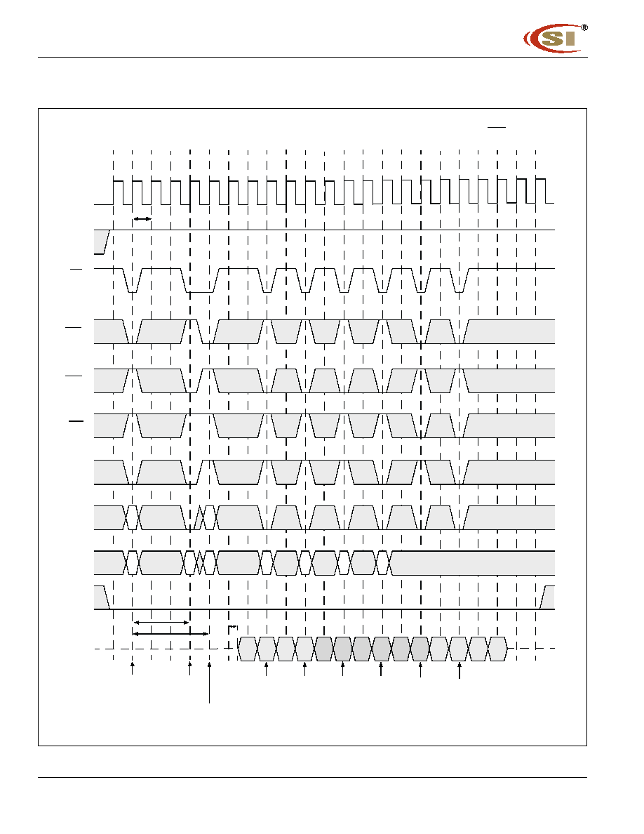
IC42S16400
52
Integrated Circuit Solution Inc.
DR034-0E 12/02/2003
Interleaved Column Read Cycle (2 of 2)
BS1="L", Bank C,D = Idle
T0 T1 T2 T3 T4 T5 T6 T7 T8 T9 T10 T11 T12 T13 T14 T15 T16 T17 T18 T19 T20 T21 T22
CLK
CKE
CS
RAS
CAS
WE
A10
ADD
DQM
DQ
t
CK3
Burst Length=4, CAS Latency=3
Activate
Bank A
Command
Hi-Z
QBb1
QAb2
QAa0 QAa1 QAa2 QAa3 QBa0 QBa1
QAb3
Precharge
Ra
Ra
Ra
Ca
Ra
Ca
Cb
Cc
Cb
QAb1
QBc0 QBc1
Read
Command
Bank A
Read
Command
Bank B
QBb0
QAb0
Read
Command
Bank B
Read
Command
Bank B
Read
Command
Bank A
Precharge
Command
Bank B
Command
Bank A
t
RRD
Activate
Command
Bank B
t
RCD
t
AC3
*BS0
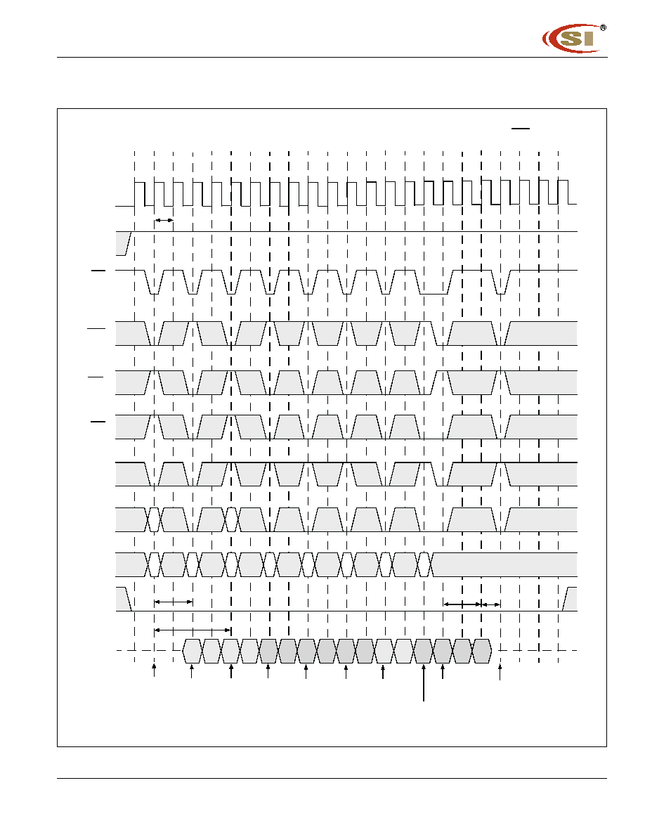
IC42S16400
Integrated Circuit Solution Inc.
53
DR034-0E 12/02/2003
Interleaved Column Write Cycle (1 of 2)
BS1="L", Bank C,D = Idle
T0 T1 T2 T3 T4 T5 T6 T7 T8 T9 T10 T11 T12 T13 T14 T15 T16 T17 T18 T19 T20 T21 T22
CLK
CKE
CS
RAS
CAS
WE
A10
ADD
DQM
DQ
t
CK2
Burst Length=4, CAS Latency=2
Activate
Bank A
Command
Hi-Z
DBb1
DBd0
DAa0 DAa1 DAa2 DAa3 DBa0 DBa1
DBd1
Precharge
Ra
Ra
Ra
Ca
Ra
Ca
Cb
Cc
Cb
DAb1
DBc0 DBc1
Write
Command
Bank A
Write
Command
Bank B
DBb0
DAb0
Command
Write
Command
Bank B
Write
Command
Bank A
Precharge
Command
Bank A
Command
Bank B
t
RRD
Activate
Command
Bank B
t
RCD
t
RP
Cb
DBd2 DBd3
Write
Bank B
t
DPL
Write
Command
Bank B
*BS0

IC42S16400
54
Integrated Circuit Solution Inc.
DR034-0E 12/02/2003
Interleaved Column Write Cycle (2 of 2)
BS1="L", Bank C,D = Idle
T0 T1 T2 T3 T4 T5 T6 T7 T8 T9 T10 T11 T12 T13 T14 T15 T16 T17 T18 T19 T20 T21 T22
CLK
CKE
CS
RAS
CAS
WE
A10
ADD
DQM
DQ
t
CK3
Burst Length=4, CAS Latency=3
Activate
Bank A
Command
Hi-Z
QBb1
QBd0
QAa0 QAa1 QAa2 QAa3 QBa0 QBa1
QBd1
Precharge
Ra
Ra
Ra
Ca
Ra
Ca
Cb
Cc
Cb
QAb1
QBc0 QBc1
Write
Command
Bank A
Write
Command
Bank B
QBb0
QAb0
Write
Command
Bank B
Write
Command
Bank B
Write
Command
Bank A
Write
Command
Bank B
Command
Bank A
t
RRD
Activate
Command
Bank B
t
RCD
Cd
t
DPL
t
RP
QBd2 QBd3
t
DPL
Precharge
Command
Bank B
*BS0

IC42S16400
Integrated Circuit Solution Inc.
55
DR034-0E 12/02/2003
Auto Precharge after Read Burst (1 of 2)
BS1="L", Bank C,D = Idle
T0 T1 T2 T3 T4 T5 T6 T7 T8 T9 T10 T11 T12 T13 T14 T15 T16 T17 T18 T19 T20 T21 T22
CLK
CKE
CS
RAS
CAS
WE
A10
ADD
DQM
DQ
t
CK2
Burst Length=4, CAS Latency=2
Activate
Bank A
Command
Hi-Z
QBa3
QBb0
QAa0 QAa1 QAa2 QAa3 QBa0 QBa1
QBb1
Read with
Ra
Ra
Ca
Ra
Ca
Cb
Rb
Cb
QAb3
QAb0 QAb1
Activate
Command
Bank B
QBa2
QAb2
Read with
Command
Bank A
Activate
Command
Bank B
Read with
Command
Bank B
Activate
Command
Bank A
Command
Bank A
Read with
Auto Precharge
Bank B
Rc
QBb2 QBb3
Rb
Rc
Ra
Cc
QAc0
QAc2
Read
Bank A
Command
Command
QAc1
Auto Precharge
Auto Precharge
Auto Precharge
Start Auto Precharge
Bank B
Start Auto Precharge
Bank A
Start Auto Precharge
Bank B
High
*BS0

IC42S16400
56
Integrated Circuit Solution Inc.
DR034-0E 12/02/2003
Auto Precharge after Read Burst (2 of 2)
BS1="L", Bank C,D = Idle
T0 T1 T2 T3 T4 T5 T6 T7 T8 T9 T10 T11 T12 T13 T14 T15 T16 T17 T18 T19 T20 T21 T22
CLK
CKE
CS
RAS
CAS
WE
A10
ADD
DQM
DQ
t
CK3
Burst Length=4, CAS Latency=3
Activate
Bank A
Command
Hi-Z
QBa3
QAa0 QAa1 QAa2 QAa3 QBa0 QBa1
Ra
Ra
Ra
QAb3
QAb0 QAb1
Read
Command
Bank A
Read with
Command
Bank B
QBa2
QAb2
Command
Bank A
Activate
Command
Bank B
QBb0
Ra
Ca
Ca
RBb
Cb
Auto Precharge
Start Auto Precharge
Bank B
Start Auto
Bank A
Start Auto Precharge
Bank B
High
Rb
Cb
QBb1 QBb2
Activate
Command
Bank B
Write with
Auto Precharge
Auto precharge
Command
Bank B
Read with
Rb
Precharge
*BS0

IC42S16400
Integrated Circuit Solution Inc.
57
DR034-0E 12/02/2003
Auto Precharge after Write Burst (1 of 2)
BS1="L", Bank C,D = Idle
T0 T1 T2 T3 T4 T5 T6 T7 T8 T9 T10 T11 T12 T13 T14 T15 T16 T17 T18 T19 T20 T21 T22
CLK
CKE
CS
RAS
CAS
WE
A10
ADD
DQM
DQ
t
CK2
Burst Length=4, CAS Latency=2
Activate
Bank A
Command
Hi-Z
QBa3
QBb0
QAa0 QAa1 QAa2 QAa3 QBa0 QBa1
QBb1
Ra
Ra
Ra
QAb3
QAb0 QAb1
Write
Command
Bank A
Write with
Command
Bank B
QBa2
QAb2
Write with
Command
Bank A
Activate
Command
Bank B
Write with
Command
Bank B
Activate
Command
Bank B
QBb2 QBb3
Rb
Ra
Ca
Cb
Ca
Rb
Cb
Auto Precharge
Auto Precharge
Auto Precharge
Start Auto Precharge
Bank B
Start Auto Precharge
Bank A
Start Auto Precharge
Bank B
High
Rc
Rc
Cc
QAc0 QAc1 QAc2 QAc3
Activate
Command
Bank A
Write with
Auto Precharge
Bank A
Start Auto
Precharge
Bank A
*BS0

IC42S16400
58
Integrated Circuit Solution Inc.
DR034-0E 12/02/2003
Auto Precharge after Write Burst (2 of 2)
BS1="L", Bank C,D = Idle
T0 T1 T2 T3 T4 T5 T6 T7 T8 T9 T10 T11 T12 T13 T14 T15 T16 T17 T18 T19 T20 T21 T22
CLK
CKE
CS
RAS
CAS
WE
A10
ADD
DQM
DQ
t
CK3
Burst Length=4, CAS Latency=3
Activate
Bank A
Command
Hi-Z
QBa3
QAa0 QAa1 QAa2 QAa3 QBa0 QBa1
Ra
Ra
Ra
QAb3
QAb0 QAb1
Read
Command
Bank A
Read with
Command
Bank B
QBa2
QAb2
Command
Bank A
Activate
Command
Bank B
QBb0
Ra
Ca
Ca
RBb
Cb
Auto Precharge
Start Auto Precharge
Bank B
Start Auto
Bank A
Start Auto Precharge
Bank B
High
Rb
Cb
QBb1 QBb2
Activate
Command
Bank B
Write with
Auto Precharge
Auto precharge
Command
Bank B
Read with
Rb
Precharge
QBb3
*BS0

IC42S16400
Integrated Circuit Solution Inc.
59
DR034-0E 12/02/2003
Full Page Read Cycle (1 of 2)
BS1="L", Bank C,D = Idle
T0 T1 T2 T3 T4 T5 T6 T7 T8 T9 T10 T11 T12 T13 T14 T15 T16 T17 T18 T19 T20 T21 T22
CLK
CKE
CS
RAS
CAS
WE
A10
ADD
DQM
DQ
t
CK2
Burst Length=Full Page, CAS Latency=2
Activate
Bank A
Command
Read
Hi-Z
Command
Ra
QAa+1
Bank A
The burst counter wraps
Burst Stop
Read
Command
Bank B
QAa
Full page burst operation does not
Ra
Ca
Rb
t
RP
High
Activate
Command
Bank B
Ra
Rb
Ca
QAa+2 QAa-2 QAa-1
QAa
QAa+1
QBa
QBa+1 QBa+2 QBa+3 QBa+4 QBa+51QBa+6
Activate
Command
Bank B
from the highest order
page address back to zero
during this time interval
terminate when the burst length is
satisfied; the burst counter
increments and continues bursting
beginning with the starting address
Command
Precharge
Command
Bank B
Ra
*BS0

IC42S16400
60
Integrated Circuit Solution Inc.
DR034-0E 12/02/2003
Full Page Read Cycle (2 of 2)
BS1="L", Bank C,D = Idle
T0 T1 T2 T3 T4 T5 T6 T7 T8 T9 T10 T11 T12 T13 T14 T15 T16 T17 T18 T19 T20 T21 T22
CLK
CKE
CS
RAS
CAS
WE
A10
ADD
DQM
DQ
t
CK3
Burst Length=Full Page, CAS Latency=3
Activate
Bank A
Command
Read
Hi-Z
Command
Ra
QAa+1
Bank A
The burst counter wraps
Burst Stop
Read
Command
Bank B
QAa
Full page burst operation
Ra
Ca
Rb
High
Activate
Command
Bank B
Ra
Rb
Ca
QAa+2 QAa-2 QAa-1
QAa
QAa+1 QBa0
QBa+1 QBa+2 QBa+3 QBa+4 QBa+5
Activate
Command
Bank B
from the highest order
page address back to zero
during this time interval
Command
Precharge
Command
Bank B
does not teminate when
the burst length is satisfied;
the burst counter increments
and continues bursting
beginning with the starting
address
Ra
*BS0

IC42S16400
Integrated Circuit Solution Inc.
61
DR034-0E 12/02/2003
Full Page Write Cycle (1 of 2)
BS1="L", Bank C,D = Idle
T0 T1 T2 T3 T4 T5 T6 T7 T8 T9 T10 T11 T12 T13 T14 T15 T16 T17 T18 T19 T20 T21 T22
CLK
CKE
CS
RAS
CAS
WE
A10
ADD
DQM
DQ
t
CK2
Burst Length=Full Page, CAS Latency=2
Activate
Bank A
Command
Write
Hi-Z
Command
Ra
QAa+1
Bank A
The burst counter wraps
Burst Stop
Write
Command
Bank B
QAa
Full page burst operation
Ra
Ca
Rb
t
BDL
High
Activate
Command
Bank B
Ra
Rb
Ca
QAa+2 QAa+3 QAa-1
QAa
QAa+1
QBa
QBa+1 QBa+2 QBa+3 QBa+4 QBa+5
Activate
Command
Bank B
from the highest order
page address back to zero
during this time interval
Command
Precharge
Command
Bank B
does not terminate when
the burst length is satisfied;
the burst counter increments
and continues bursting
beginning with the starting
address
QBa+6
Data is ignored
Ra
*BS0

IC42S16400
62
Integrated Circuit Solution Inc.
DR034-0E 12/02/2003
Full Page Write Cycle (2 of 2)
BS1="L", Bank C,D = Idle
T0 T1 T2 T3 T4 T5 T6 T7 T8 T9 T10 T11 T12 T13 T14 T15 T16 T17 T18 T19 T20 T21 T22
CLK
CKE
CS
RAS
CAS
WE
A10
ADD
DQM
DQ
t
CK3
Burst Length=Full Page, CAS Latency=3
Activate
Bank A
Command
Write
Hi-Z
Command
Ra
DAa+1
Bank A
The burst counter wraps
Burst Stop
Write
Command
Bank B
DAa
Full page burst operation
Ra
tBDL
High
Activate
Command
Bank B
DAa+2 DAa+3 DAa-1
DAa
DAa+1
DBa
DBa+1 DBa+2 DBa+3 DBa+4 DBa+5
Activate
Command
Bank B
from the highest order
page address back to zero
during this time interval
Command
Precharge
Command
Bank B
does not terminate when
the burst length is satisfied;
the burst counter increments
and continues bursting
beginning with the starting
address
Ra
Rb
Ca
Ra
Ca
Rb
Data is ignored.
*BS0

IC42S16400
Integrated Circuit Solution Inc.
63
DR034-0E 12/02/2003
Burst Read and Single Write Operation
BS1="L", Bank C,D = Idle
Hi-Z
T0 T1 T2 T3 T4 T5 T6 T7 T8 T9 T10 T11 T12 T13 T14 T15 T16 T17 T18 T19 T20 T21 T22
CLK
CKE
CS
RAS
CAS
WE
A10
ADD
DQM
t
CK2
Burst Length=4, CAS Latency=2
RAa
RAa
High
Activate
CAa
CAb
CAd
DQ
Command
Bank A
Read
Command
Bank A
Single Write Single Write
Read
Command
Bank A
DQs are
masked
CAc
CAe
Command
Bank A
Command
Bank A
Single Write
Command
Bank A
DQs are
masked
*BS0

IC42S16400
64
Integrated Circuit Solution Inc.
DR034-0E 12/02/2003
Full Page Random Column Read
BS1="L", Bank C,D = Idle
T0 T1 T2 T3 T4 T5 T6 T7 T8 T9 T10 T11 T12 T13 T14 T15 T16 T17 T18 T19 T20 T21 T22
CLK
CKE
CS
RAS
CAS
WE
BS
A10
ADD
DQM
DQ
t
CK2
Burst Length=Full Page, CAS Latency=2
Activate
Bank A
Command
Activate
Hi-Z
Command
Ra
QBa0
Bank B
Read
Command
Bank B
QAa0
Ra
Activate
Command
Bank B
QAb0
QAb1
QBb0
QBb1
QAc0
QAc1
QAc2
QBc0
QBc1
QBc2
Read
Command
Bank A
Precharge
Cc
Cc
Rb
Ra
Ra
Ca
Ca
Cb
Cb
Rb
t
RP
Read
Command
Bank B
Read
Command
Bank A
Read
Command
Bank A
Read
Command
Bank B
Command Bank B
(Precharge Termination)
(Bank D)
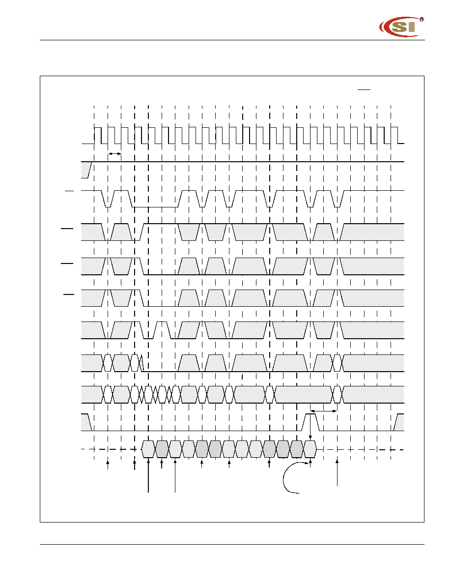
IC42S16400
Integrated Circuit Solution Inc.
65
DR034-0E 12/02/2003
Full Page Random Column Write
BS1="L", Bank C,D = Idle
T0 T1 T2 T3 T4 T5 T6 T7 T8 T9 T10 T11 T12 T13 T14 T15 T16 T17 T18 T19 T20 T21 T22
CLK
CKE
CS
RAS
CAS
WE
A10
ADD
DQM
DQ
t
CK2
Burst Length=Full Page, CAS Latency=2
Activate
Bank A
Command
Activate
Hi-Z
Command
Ra
QBa0
Bank B
Write
Command
Bank B
QAa0
Ra
Activate
Command
Bank B
QAb0
QAb1
QBb0
QBb1
QAc0
QAc1
QAc2
QBc0
QBc1
QBc2
Write
Command
Bank A
Precharge
Cc
Cc
Rb
Ra
Ra
Ca
Ca
Cb
Cb
Rb
t
RP
Write
Command
Bank B
Write
Command
Bank A
Write
Command
Bank A
Write
Command
Bank B
Command Bank B
(Precharge Termination)
Write Data
is masked
(Bank D)
*BS0
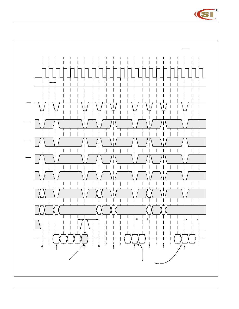
IC42S16400
66
Integrated Circuit Solution Inc.
DR034-0E 12/02/2003
Precharge Termination of a Burst (1 of 2)
BS1="L", Bank C,D = Idle
T0 T1 T2 T3 T4 T5 T6 T7 T8 T9 T10 T11 T12 T13 T14 T15 T16 T17 T18 T19 T20 T21 T22
CLK
CKE
CS
RAS
CAS
WE
A10
ADD
DQM
DQ
t
CK2
Burst Length=8, CAS Latency=2
Activate
Bank A
Command
Write
Hi-Z
Command
RAa
Bank A
Activate
Command
Bank A
Read
Command
Bank A
RAc
CAb
RAb
RAb
RAc
Precharge Termination
of a Write Burst. Write
data is masked.
Precharge
Command
Read
Command
Bank A
Precharge
Command
Bank A
Precharge Termination
High
RAa
CAc
CAa
QAa1
QAa0
QAa2
Da3
QAb0
QAb1
QAb2
QAc0
QAc1
QAc2
t
DPL
t
RP
t
RP
t
RP
Bank A
of a Read Burst.
Activate
Command
Bank A
Precharge
Command
Bank A
*BS0

IC42S16400
Integrated Circuit Solution Inc.
67
DR034-0E 12/02/2003
Precharge Termination of a Burst (2 of 2)
BS1="L", Bank C,D = Idle
T0 T1 T2 T3 T4 T5 T6 T7 T8 T9 T10 T11 T12 T13 T14 T15 T16 T17 T18 T19 T20 T21 T22
CLK
CKE
CS
RAS
CAS
WE
A10
ADD
DQM
DQ
t
CK3
Activate
Bank A
Command
Write
Hi-Z
Command
RAa
Bank A
Activate
Command
Bank A
CAb
RAb
RAb
RAc
Precharge
Command
Read
Command
Bank A
High
RAa
RAc
CAa
DAa1
DAa0
QAb0
QAb1
QAb2
QAb3
tDPL
t
RP
Bank A
Activate
Command
Bank A
Activate
Command
Bank A
t
RCD
t
RP
Write Data
is masked
Precharge Termination
of a Write Burst.
Precharge Termination
of a Read Burst.
t
RAS
*BS0
Burst Length=8, CAS Latency=3

IC42S16400
68
Integrated Circuit Solution Inc.
DR034-0E 12/02/2003
ORDERING INFORMATION
Commercial Range: 0
C to 70
C
Speed (ns)
Order Part No.
Package
6
IC42S16400-6T
400mil TSOP-2
IC42S16400-6TG
400mil TSOP-2(Pb-free)
IC42S16400-6BG
60Ball VF-BGA(Pb-free)
7
IC42S16400-7T
400mil TSOP-2
IC42S16400-7TG
400mil TSOP-2(Pb-free)
IC42S16400-7BG
60Ball VF-BGA(Pb-free)
ORDERING INFORMATION
Industrial Temperature Range: -40
C to 85
C
Speed (ns)
Order Part No.
Package
6
IC42S16400-6TI
400mil TSOP-2
IC42S16400-6TIG
400mil TSOP-2(Pb-free)
IC42S16400-6BIG
60Ball VF-BGA(Pb-free)
7
IC42S16400-7TI
400mil TSOP-2
IC42S16400-7TIG
400mil TSOP-2(Pb-free)
IC42S16400-7BIG
60Ball VF-BGA(Pb-free)
Integrated Circuit Solution Inc.
HEADQUARTER:
NO.2, TECHNOLOGY RD. V, SCIENCE-BASED INDUSTRIAL PARK,
HSIN-CHU, TAIWAN, R.O.C.
TEL: 886-3-5780333
Fax: 886-3-5783000
BRANCH OFFICE:
7F, NO. 106, SEC. 1, HSIN-TAI 5
TH
ROAD,
HSICHIH TAIPEI COUNTY, TAIWAN, R.O.C.
TEL: 886-2-26962140
FAX: 886-2-26962252
http://www.icsi.com.tw