
IC42S32400
IC42S32400L
Integrated Circuit Solution Inc.
1
DR038-0C 02/01/2005
Document Title
1M x 32 Bit x 4 Banks (128-MBIT) SDRAM
Revision History
Revision No
History
Draft Date
Remark
0A
Initial Draft
December 01,2003
0B
Revise Page22 typo
December 21,2004
0C
Revise p.22 data and p.28 typo
February 01,2005
The attached datasheets are provided by ICSI. Integrated Circuit Solution Inc reserve the right to change the specifications and
products. ICSI will answer to your questions about device. If you have any questions, please contact the ICSI offices.

IC42S32400
IC42S32400L
2
Integrated Circuit Solution Inc.
DR038-0C 02/01/2005
ICSI reserves the right to make changes to its products at any time without notice in order to improve design and supply the best possible product. We assume no responsibility for any errors
which may appear in this publication. � Copyright 2000, Integrated Circuit Solution Inc.
1M Words x 32 Bits x 4 Banks (128-MBIT)
SYNCHRONOUS DYNAMIC RAM
FEATURES
� Concurrent auto precharge
� Clock rate:166/143/125 MHz
� Fully synchronous operation
� Internal pipelined architecture
� Four internal banks (1M x 32bit x 4bank)
� Programmable Mode
-CAS#Latency:2 or 3
-Burst Length:1,2,4,8,or full page
-Burst Type:interleaved or linear burst
-Burst-Read-Single-Write
� Burst stop function
� Individual byte controlled by DQM0-3
� Auto Refresh and Self Refresh
� 4096 refresh cycles/64ms
� Single +3.3V �0.3V power supply
� Interface:LVTTL
� Package:400 x 875 mil,86 Pin TSOP-2,0.50mm Pin
Pitch and 11x13mm, 90 Ball BGA, Ball pitch 0.8mm
� Pb-free package is available.
DESCRIPTION
The ICSI IC42S32400 and IC42S32400L is a high-speed
CMOS configured as a quad 1M x 32 DRAM with a
synchronous interface (all signals are registered on the
positive edge of the clock signal,CLK).
Each of the 1M x 32 bit banks is organized as 4096 rows
by 256 columns by 32 bits.Read and write accesses start
at a selected locations in a programmed sequence.
Accesses begin with the registration of a BankActive
command which is then followed by a Read or Write
command
The ICSI IC42S32400 and IC42S32400L provides for
programmable Read or Write burst lengths of 1,2,4,8,or
full page, with a burst termination operation. An auto
precharge function may be enable to provide a self-timed
row precharge that is initiated at the end of the burst
sequence.The refresh functions,either Auto or Self
Refresh are easy to use.
By having a programmable mode register,the system
can choose the most suitable modes to maximize its
performance.
These devices are well suited for applications requiring
high memory bandwidth.
IC42S32400
IC42S32400L
Integrated Circuit Solution Inc.
3
DR038-0C 02/01/2005
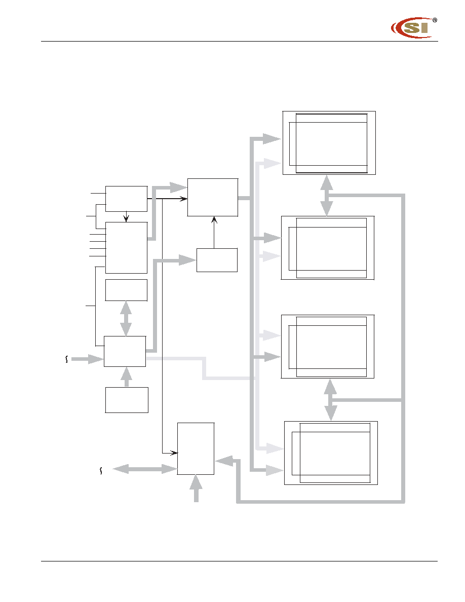
FUNCTIONAL BLOCK DIAGRAM
COLUMN
C O U N TE R
A D D R E S S
B U F F E R
A 0
A 9
B S 0
B S 1
D Q M 0 ~ 3
C L O C K
B U F F E R
COMMAND
D E C O D E R
Sense Amplifier
Row
Dec
oder
Sense Amplifier
Column Decoder
Row Decoder
CLK
C K E
C S #
R A S #
C A S #
W E #
D Q 0
D Q 31
Sense Amplifier
Col um n Decoder
Row Decoder
Sense Amplifier
Column Decoder
Row Decoder
4096 X 256 X 32
CELL ARRAY
(BANK #2)
D Q
B U F F E R
A 1 0 / A P
R E F R E S H
C O U N T E R
M O D E
R E G I S T E R
C O N T R O L
S I G N A L
G E N E R AT O R
C o l u m n D e c o d e r
4 0 9 6 X 2 5 6 X 3 2
C E L L A R R AY
( B A N K # 0 )
4 0 9 6 X 2 5 6 X 3 2
C E L L A R R AY
( B A N K # 1 )
4096 X 256 X 32
CELL ARRAY
(BANK #3)
A 1 1

IC42S32400
IC42S32400L
4
Integrated Circuit Solution Inc.
DR038-0C 02/01/2005
PIN DESCRIPTIONS
Table 1.Pin Details of IC42S32400 and IC42S32400L
Symbol
Type
Description
CLK
Input
Clock:CLK is driven by the system clock.All SDRAM input signals are sampled on the positive edge
of CLK.CLK also increments the internal burst counter and controls the output registers.
CKE
Input
Clock Enable:CKE activates(HIGH)and deactivates(LOW)the CLK signal.If CKE goes low syn-
chronously with clock(set-up and hold time same as other inputs),the internal clock is suspended
from the next clock cycle and the state of output and burst address is frozen as long as the CKE
remains low.When all banks are in the idle state,deactivating the clock controls the entry to the
Power Down and Self Refresh modes.CKE is synchronous except after the device enters Power
Down and Self Refresh modes,where CKE becomes asynchronous until exiting the same mode.
The input buffers,including CLK,are disabled during Power Down and Self Refresh modes,providing
low standby power.
BS0,BS1 Input
Bank Select:BS0 and BS1 defines to which bank the BankActivate,Read,Write,or BankPrecharge
command is being applied.
A0-A11 Input
Address Inputs:A0-A11 are sampled during the BankActivate command (row address A0-A11)and
Read/Write command (column address A0-A7 with A10 defining Auto Precharge) to select one
location in the respective bank.During a Precharge command,A10 is sampled to determine if all
banks are to be precharged (A10 =HIGH).
The address inputs also provide the op-code during a Mode Register Set .
CS#
Input
Chip Select:CS#enables (sampled LOW)and disables (sampled HIGH)the command decoder.All
commands are masked when CS#is sampled HIGH.CS#provides for external bank selection on
systems with multiple banks.It is considered part of the command code.
RAS#
Input
Row Address Strobe:The RAS#signal defines the operation commands in conjunction with the
CAS#and WE#signals and is latched at the positive edges of CLK.When RAS# and CS#are as-
serted "LOW"and CAS#is asserted "HIGH,"either the BankActivate command or the Precharge
command is selected by the WE#signal.When the WE#is asserted "HIGH,"the BankActivate com-
mand is selected and the bank designated by BS is turned on to the active state.When the WE#is
asserted "LOW,"the Precharge command is selected and the bank designated by BS is switched to
the idle state after the precharge operation.
CAS#
Input
Column Address Strobe:The CAS#signal defines the operation commands in conjunction with the
RAS#and WE#signals and is latched at the positive edges of CLK. When RAS#is held "HIGH"and
CS#is asserted "LOW,"the column access is started by asserting CAS#"LOW."Then,the Read or
Write command is selected by asserting WE# "LOW"or "HIGH."
WE#
Input
Write Enable:The WE#signal defines the operation commands in conjunction with the RAS#and
CAS#signals and is latched at the positive edges of CLK.The WE#input is used to select the
BankActivate or Precharge command and Read or Write command.
DQM0-3 Input
Data Input/Output Mask:DQM0-DQM3 are byte specific,nonpersistent I/O buffer controls. The I/O
buffers are placed in a high-z state when DQM is sampled HIGH.Input data is masked when DQM
is sampled HIGH during a write cycle.Output data is masked (two-clock latency)when DQM is
sampled HIGH during a read cycle.DQM3 masks DQ31-DQ24,DQM2 masks DQ23-DQ16,DQM1
masks DQ15-DQ8,and DQM0 masks DQ7-DQ0.
DQ0-31 Input/Output
Data I/O:The DQ0-31 input and output data are synchronized with the positive edges of
CLK.The I/Os are byte-maskable during Reads and Writes.
IC42S32400
IC42S32400L
Integrated Circuit Solution Inc.
5
DR038-0C 02/01/2005
PIN FUNCTION
NC
-
No Connect:These pins should be left unconnected.
VDDQ
Supply
DQ Power:Provide isolated power to DQs for improved noise immunity.
VSSQ
Supply
DQ Ground:Provide isolated ground to DQs for improved noise immunity.
VDD
Supply
Power Supply:+3.3V � 0.3V
VSS
Supply
Ground
Pin Assignment (Top View)
VDD
DQ0
VDDQ
DQ1
DQ2
VSSQ
DQ3
DQ4
VDDQ
DQ5
DQ6
VSSQ
DQ7
NC
VDD
DQM 0
/WE
/CAS
/RAS
/CS
A11
BS0
BS1
A10/AP
A 0
A 1
A 2
DQM 2
VDD
NC
DQ16
VSSQ
DQ17
DQ18
VDDQ
DQ19
DQ20
VSSQ
DQ21
DQ22
VDDQ
DQ23
VDD
VSS
DQ15
VSSQ
DQ14
DQ13
VDDQ
DQ12
DQ11
VSSQ
DQ10
DQ9
VDDQ
DQ8
NC
VSS
DQM1
NC
NC
CL K
CKE
A 9
A 8
A 7
A 6
A 5
A 4
A 3
DQM3
VSS
NC
DQ31
VDDQ
DQ30
DQ29
VSSQ
DQ28
DQ27
VDDQ
DQ26
DQ25
VSSQ
DQ24
VSS
1
2
3
4
5
6
7
8
9
1 0
11
1 2
1 3
1 4
1 5
1 6
1 7
1 8
1 9
2 0
2 1
2 2
2 3
2 4
2 5
2 6
2 7
2 8
2 9
3 0
3 1
3 2
3 3
3 4
3 5
3 6
3 7
3 8
3 9
4 0
4 1
4 2
4 3
8 6
8 5
8 4
8 3
8 2
8 1
8 0
7 9
7 8
7 7
7 6
7 5
7 4
7 3
7 2
7 1
7 0
6 9
6 8
6 7
6 6
6 5
6 4
6 3
6 2
6 1
6 0
5 9
5 8
5 7
5 6
5 5
5 4
5 3
5 2
5 1
5 0
4 9
4 8
4 7
4 6
4 5
4 4
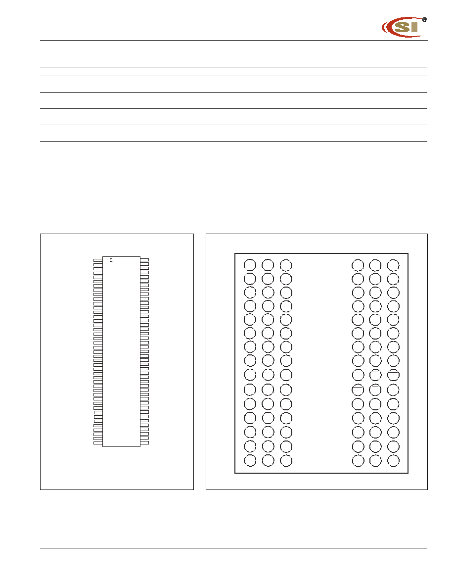
PIN CONFIGURATIONS
86-Pin TSOP 2
90-Ball FBGA
1 2 3 4 5 6 7 8 9
A
B
C
D
E
F
G
H
J
K
L
M
N
P
R
(Top View)
DQ
26
DQ
24
Vss
DQ
28
V
DDQ
V
SSQ
V
SSQ
DQ
27
DQ
25
V
SSQ
DQ
29
DQ
30
V
DDQ
DQ
31
NC
V
SS
DQM
3
A3
A4
A5
A6
A7
A8
NC
V
DD
DQ
23
DQ
21
V
DDQ
V
SSQ
DQ
19
DQ
22
DQ
20
V
DDQ
DQ
17
DQ
18
V
DDQ
NC
DQ
16
V
SSQ
A2
DQM
2
V
DD
A10
A0
A1
NC
BA1
A11
CLK
CKE
A9
DQM1
NC
NC
V
DDQ
DQ
8
V
SS
V
SSQ
DQ
10
DQ
9
V
SSQ
DQ
12
DQ
14
BA0
CS
RAS
CAS
WE
DQM
0
V
DD
DQ
7
V
SSQ
DQ
6
DQ
5
V
DDQ
DQ
1
DQ
3
V
DDQ
DQ11
V
DDQ
V
SSQ
DQ13
DQ
15
V
SS
V
DDQ
V
SSQ
DQ
4
V
DD
DQ
0
DQ
2

IC42S32400
IC42S32400L
6
Integrated Circuit Solution Inc.
DR038-0C 02/01/2005
Operation Mode
Fully synchronous operations are performed to latch the commands at the positive edges of CLK.Table 2 shows the truth
table for the operation commands.
Table 2.Truth Table (Note (1),(2))
Note:
1. V =Valid,X =Don 't care,L =Logic low,H =Logic high
2. CKEn signal is input level when commands are provided.
CKEn-1 signal is input level one clock cycle before the commands are provided.
3. These are states of bank designated by BS signal.
4. Device state is 1,2,4,8,and full page burst operation.
5. Power Down Mode can not enter in the burst operation.
When this command is asserted in the burst cycle,device state is clock suspend mode.
6. DQM0-3
Command
State
CKEn-1 CKE
DQM
(6)
BS0,1
A10 A11,A9-0
CS# RAS# CAS# WE#
BankActivate
Idle
(3)
H
X
X
V
Row address
L
L
H
H
BankPrecharge
Any
H
X
X
V
L
X
L
L
H
L
PrechargeAll
Any
H
X
X
X
H
X
L
L
H
L
Write
Active
(3)
H
X
X
V
L
L
H
L
L
Write and Auto Precharge Active
(3)
H
X
X
V
H
L
H
L
L
Read
Active
(3)
H
X
X
V
L
L
H
L
H
Read and Autoprecharge
Active
(3)
H
X
X
V
H
L
H
L
H
Mode Register
Set Idle
H
X
X
OP code
L
L
L
L
No-Operation
Any
H
X
X
X
X
X
L
H
H
H
Burst Stop
Active
(4)
H
X
X
X
X
X
L
H
H
L
Device Deselect
Any
H
X
X
X
X
X
H
X
X
X
AutoRefresh
Idle
H
H
X
X
X
X
L
L
L
H
SelfRefresh Entry
Idle
H
L
X
X
X
X
L
L
L
H
SelfRefresh Exit
Idle
L
H
X
X
X
X
H
X
X
X
(SelfRefresh)
L
H
H
H
Clock Suspend Mode Entry Active
H
L
X
X
X
X
X
X
X
X
Power Down Mode Entry
Any
(5)
H
L
X
X
X
X
H
X
X
X
L
H
H
H
Clock Suspend Mode Exit Active
L
H
X
X
X
X
X
X
X
X
Power Down Mode Exit
Any
L
H
X
X
X
X
H
X
X
X
(PowerDown)
L
H
H
H
Data Write/Output Enable Active
H
X
L
X
X
X
X
X
X
X
Data Mask/Output Disable Active
H
X
H
X
X
X
X
X
X
X
Column
address
(A0 ~A7)
Column
address
(A0 ~A7)
IC42S32400
IC42S32400L
Integrated Circuit Solution Inc.
7
DR038-0C 02/01/2005
Commands
1
BankActivate
(RAS#="L",CAS#="H",WE#="H",BS =Bank,A0-A11 =Row Address)
The BankActivate command activates the idle bank designated by the BS0,1 (Bank Select) signal.By latching the
row address on A0 to A11 at the time of this command,the selected row access is initiated.The read or write
operation in the same bank can occur after a time delay of tRCD(min.)from the time of bank activation.A
subsequent BankActivate command to a different row in the same bank can only be issued after the previous
active row has been precharged (refer to the following figure).The minimum time interval between successive
BankActivate commands to the same bank is defined by tRC(min.).The SDRAM has four internal banks on the
same chip and shares part of the internal circuitry to reduce chip area;therefore it restricts the back-to-back
activation of the four banks.tRRD(min.)specifies the minimum time required between activating different banks.
After this command is used,the Write command and the Block Write command perform the no mask write
operation.
CLK
ADDRESS
T0
T1
T2
T3
Tn+3
Tn+4
Tn+5
Tn+6
..............
COMMAND
..............
..............
NOP
NOP
NOP
NOP
RAS# - CAS# delay (
t
RCD
)
RAS#- RAS# delay time (
t
RRD
)
RAS# Cycle time (
t
RC
)
Bank A
Row Addr.
Bank A
Col Addr.
Bank B
Row Addr.
Bank A
Row Addr.
Bank A
Activate
R/W A with
AutoPrecharge
Bank B
Activate
Bank A
Activate
Auto Precharge
Begin
:"H" or "L"
Bank
2
BankPrecharge command
(RAS#="L",CAS#="H",WE#="L",BS =Bank,A10 ="L")
The BankPrecharge command precharges the bank disignated by BS0,1 signal.The
precharged bank is switched from the active state to the idle state.This command can be asserted anytime after
tRAS(min.)is satisfied from the BankActivate command in the desired bank.The maximum time any bank can be
active is specified by tRAS(max.).Therefore,the precharge function must be performed in any active bank within
tRAS(max.).At the end of precharge,the precharged bank is still in the idle state and is ready to be activated again.

IC42S32400
IC42S32400L
8
Integrated Circuit Solution Inc.
DR038-0C 02/01/2005
3
PrechargeAll command
(RAS#="L",CAS#="H",WE#="L",BS =Don t care,A10 ="H")
The PrechargeAll command precharges all the four banks simultaneously and can be issued even if all banks are
not in the active state.All banks are then switched to the idle state.
4
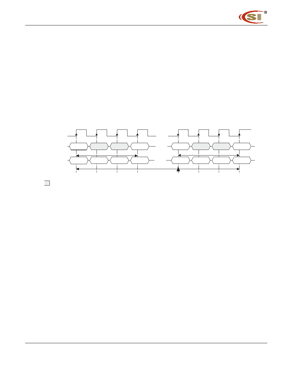
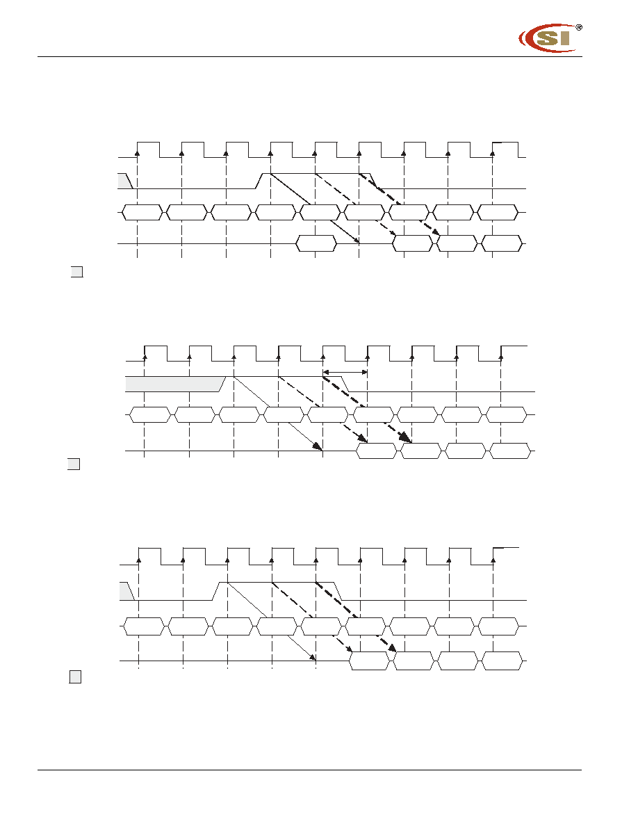
Read command
(RAS#="H",CAS#="L",WE#="H",BS =Bank,A10 ="L",A0-A7 =Column Address)
The Read command is used to read a burst of data on consecutive clock cycles from an active row in an active
bank.The bank must be active for at least tRCD(min.)before the Read command is issued.During read bursts,
the valid data-out element from the starting column address will be available following the CAS#latency after the
issue of the Read command.Each subsequent data- out element will be valid by the next positive clock edge (refer
to the following figure).The DQs go
into high-impedance at the end of the burst unless other command is
initiated.The burst length,burst sequence,and CAS#latency are determined by the mode register which is already
programmed.A full-page burst will continue until terminated (at the end of the page it will wrap to
column 0 and continue).
IC42S32400
IC42S32400L
Integrated Circuit Solution Inc.
9
DR038-0C 02/01/2005
T0
T2
T1
T3
T4
T5
T6
T7
T8
READ A
NOP
NOP
NOP
NOP
NOP
NOP
NOP
NOP
DOUT A0
DOUT A1
DOUT A2
DOUT A3
DOUT A0
DOUT A1
DOUT A2
DOUT A3
CLK
COMMAND
CAS# latency=2
tCK2, DQ s
CAS# latency=3
tCK3, DQ s
READ A
READ B
NOP
NOP
NOP
NOP
NOP
NOP
NOP
DOUT A0
DOUT B0
DOUT B1
DOUT B2
DOUT B3
DOUT A0
DOUT B0
DOUT B1
DOUT B3
2
DOUT B
CLK
COMMAND
CAS# latency=2
tCK2, DQ s
CAS# latency=3
tCK3, DQ s
T0
T2
T1
T3
T4
T5
T6
T7
T8
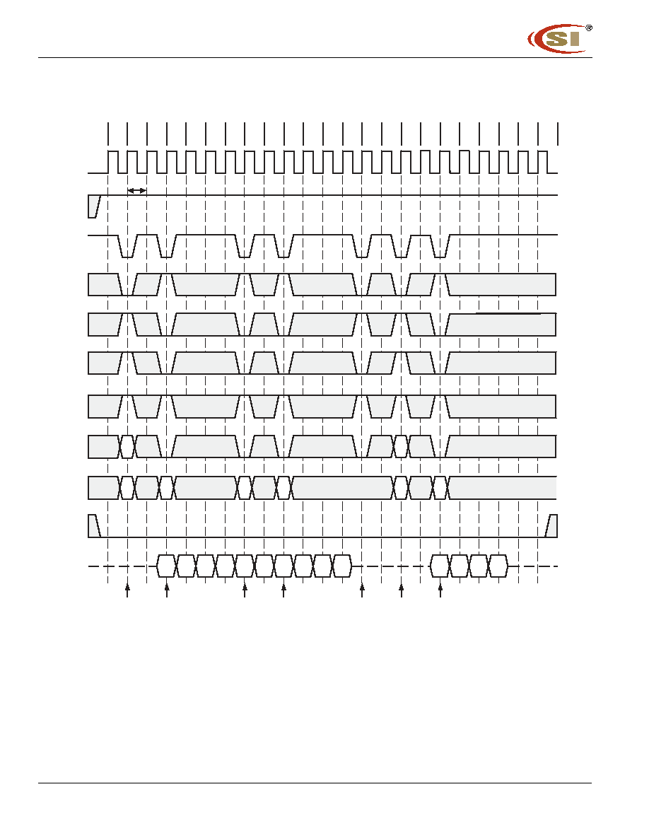
Burst Read Operation(Burst Length =4,CAS#Latency =2,3)
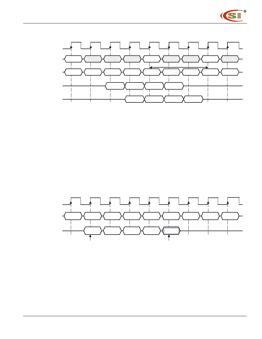
The read data appears on the DQs subject to the values on the DQM inputs two clocks earlier (i.e.DQM latency is two clocks
for output buffers).A read burst without the auto precharge function may be interrupted by a subsequent Read or Write
command to the same bank or the other active bank before the end of the burst length.It may be interrupted by a
BankPrecharge/PrechargeAll command to the same bank too.The interrupt coming from the Read command can occur on
any clock cycle following a previous Read command (refer to the following figure).
Read Interrupted by a Read (Burst Length =4,CAS#Latency =2,3)
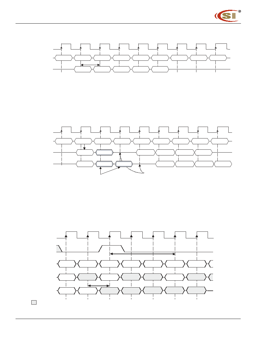
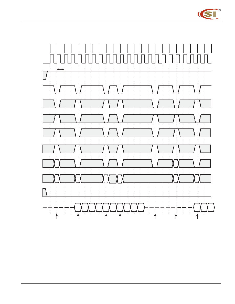
The DQM inputs are used to avoid I/O contention on the DQ pins when the interrupt comes from a Write command.The
DQMs must be asserted (HIGH)at least two clocks prior to the Write command to suppress data-out on the DQ pins.To
guarantee the DQ pins against I/O contention,a single cycle with high-impedance on the DQ pins must occur between the
last read data and the Write command (refer to the following three figures).If the data output of the burst read occurs at the
second clock of the burst write,the DQMs must be asserted (HIGH)at least one clock prior to the Write command to avoid
internal bus contention.
IC42S32400
IC42S32400L
10
Integrated Circuit Solution Inc.
DR038-0C 02/01/2005
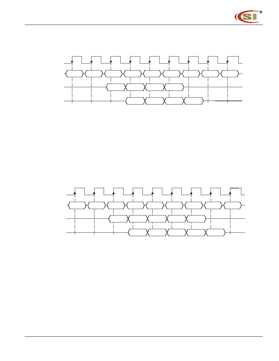
READ A
NOP
NOP
NOP
NOP
WRITE B
NOP
NOP
DQM
COMMAND
DQ's
NOP
DOUT A
DINB 2
DINB 1
DINB 0
Must be Hi-Z before
the Write Command
: "H" or "L"
CLK
T0
T2
T1
T3
T4
T5
T6
T7
T8
CLK
DQM
COMMAND
NOP
NOP
NOP
NOP
NOP
BANKA
ACTIVAT E
DIN A 0
DIN A 1
DIN A 2
DIN A 3
1 Clk Interval
CAS# latency=2
READ A
WRITEA
: "H" or "L"
NOP
T0
T2
T1
T3
T4
T5
T6
T7
T8
tCK2, DQs
CLK
DQM
COMMAND
NOP
READ A
NOP
NOP
NOP
NOP
DIN B0
DIN B1
DIN B2
DIN B3
CAS# latency=2
NOP
NOP
: "H" or "L"
tCK2, DQ's
T0
T2
T1
T3
T4
T5
T6
T7
T8
WRITEB
tCK2, DQs
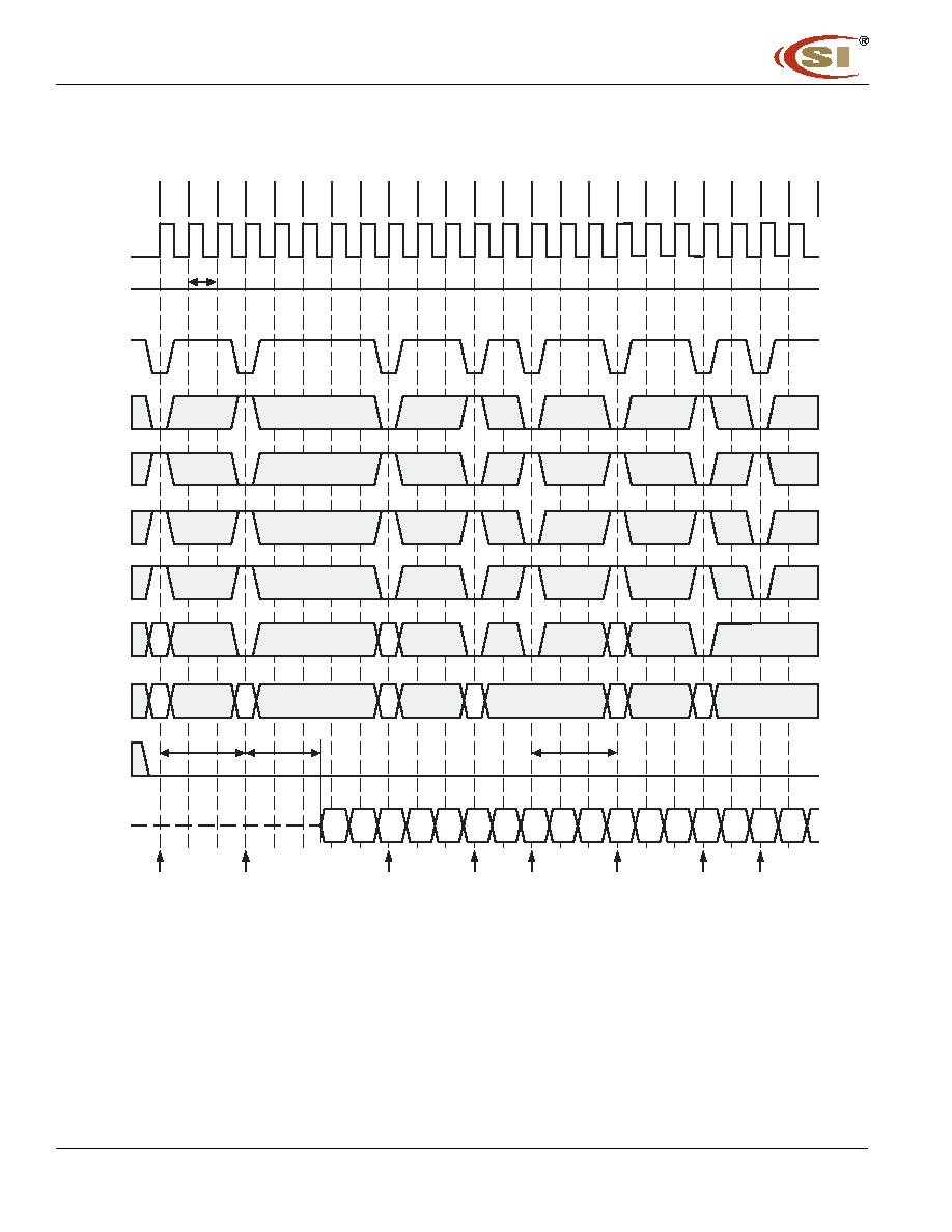
Read to Write Interval (Burst Length = 4,CAS#Latency =3)
Read to Write Interval (Burst Length = 4,CAS#Latency =2)
Read to Write Interval (Burst Length = 4,CAS#Latency =2)
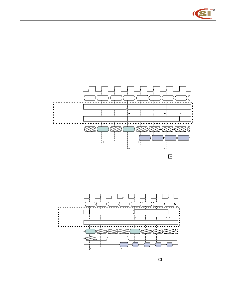
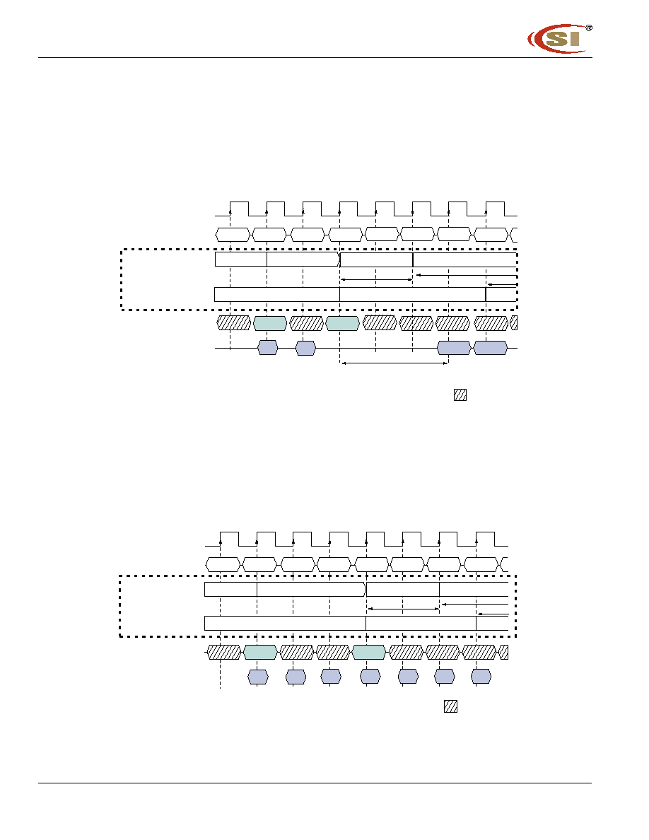
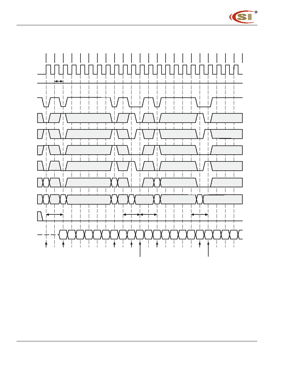
A read burst without the auto precharge function may be interrupted by a BankPrecharge/
PrechargeAll command to the same bank.The following figure shows the optimum time that
BankPrecharge/PrechargeAll command is issued in different CAS#latency.
IC42S32400
IC42S32400L
Integrated Circuit Solution Inc.
11
DR038-0C 02/01/2005
Read to Precharge (CAS#Latency =2,3)
5
Write command
(RAS#="H",CAS#="L",WE#="L",BS =Bank,A10 ="L",A0-A7 =Column Address)
The Write command is used to write a burst of data on consecutive clock cycles from an active row in an active
bank.The bank must be active for at least tRCD(min.)before the Write command is issued.During write bursts,
the first valid data-in element will be registered coincident with the Write command.Subsequent data elements
will be registered on each successive positive clock edge (refer to the following figure).The DQs remain with high-
impedance at the end of the burst unless another command is initiated.The burst length and burst sequence are
determined by the mode register,which is already programmed.A full-page burst will continue until terminated (at
the end of the page it will wrap to column 0 and continue).
CLK
COMMAND
READ A
NOP
NOP
NOP
NOP
Activate
NOP
NOP
Precharge
DOUT A0
DOUT A1
DOUT A2
DOUT A3
DOUT A0
DOUT A1
DOUT A2
DOUT A3
ADDRESS
t
RP
Bank,
Col A
Bank(s)
CAS# latency=2
tCK2, DQ s
CAS# latency=3
tCK3, DQ s
T0
T2
T1
T3
T4
T5
T6
T7
T8
Bank,
Row
CLK
COMMAND
DIN A 3
NOP
WRITEA
I
NOP
NOP
NOP
NOP
NOP
NOP
NOP
DIN A 0
DIN A 1
DIN A 2
DQ0 - DQ3
The first data element and the write
are registered on the same clock edge.
Extra data is masked.
don't care
T0
T2
T1
T3
T4
T5
T6
T7
T8
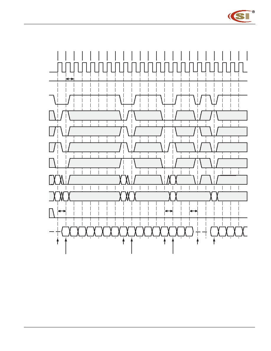
Burst Write Operation (Burst Length =4,CAS#Latency =2,3)
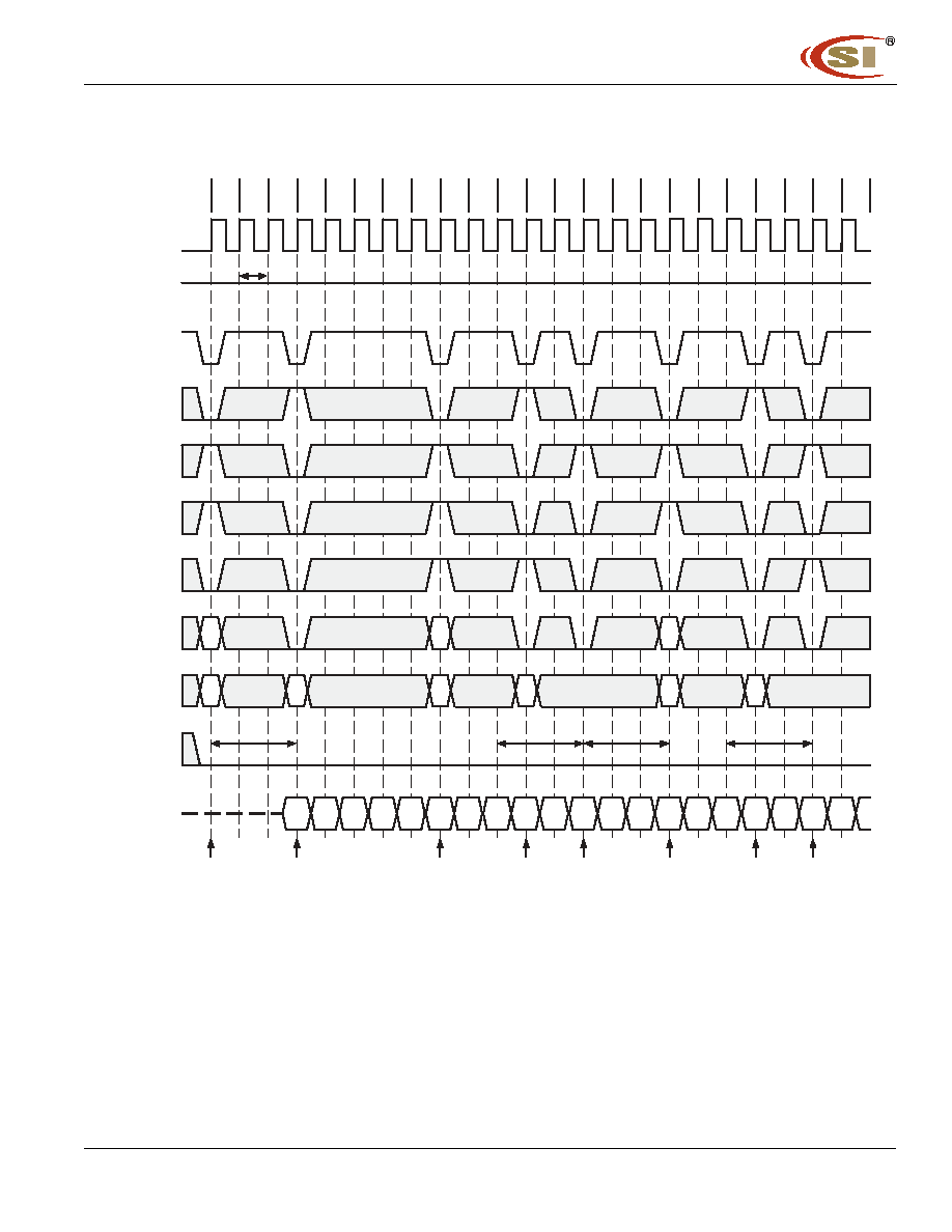
A write burst without the AutoPrecharge function may be interrupted by a subsequent Write, BankPrecharge/
PrechargeAll,or Read command before the end of the burst length.An interrupt coming from Write command can
occur on any clock cycle following the previous Write command (refer to the following figure).
IC42S32400
IC42S32400L
12
Integrated Circuit Solution Inc.
DR038-0C 02/01/2005
CLK
COMMAND
DIN B2
NOP
WRITEA
WRITEB
NOP
NOP
NOP
NOP
NOP
NOP
DIN A0
DIN B0
DIN B1
DQ's
DIN B3
1 Clk Interval
T0
T2
T1
T3
T4
T5
T6
T7
T8
CLK
COMMAND
T0
T 1
T2
T3
T4
T5
T6
T7
T8
NOP
WRITEA
NOP
NOP
NOP
NOP
NOP
READ B
NOP
DIN A0
don't care
DOUT B2
DOUT B0
DOUT B1
DOUT B3
DIN A0
don't care
don't care
DOUT B2
DOUT B0
DOUT B1
DOUT B3
DI N
Input data must be removed from the DQs at least one clock
cycle before the Read data appears on the outputs to avoid
data contention.
Input data for the write is masked.
CAS# latency=2
tCK2, DQ's
CAS# latency=3
tCK3 , DQ's
CLK
WRITE
COMMAND
BANK (S)
ROW
NOP
NOP
Precharge
NOP
NOP
Activate
BANK
COL n
DIN
n
n + 1
DQM
ADDRESS
DQ
tWR
tRP
: don t care
T0
T2
T1
T3
T4
T5
T6
Write Interrupted by a Write (Burst Length =4,CAS#Latency =2,3)
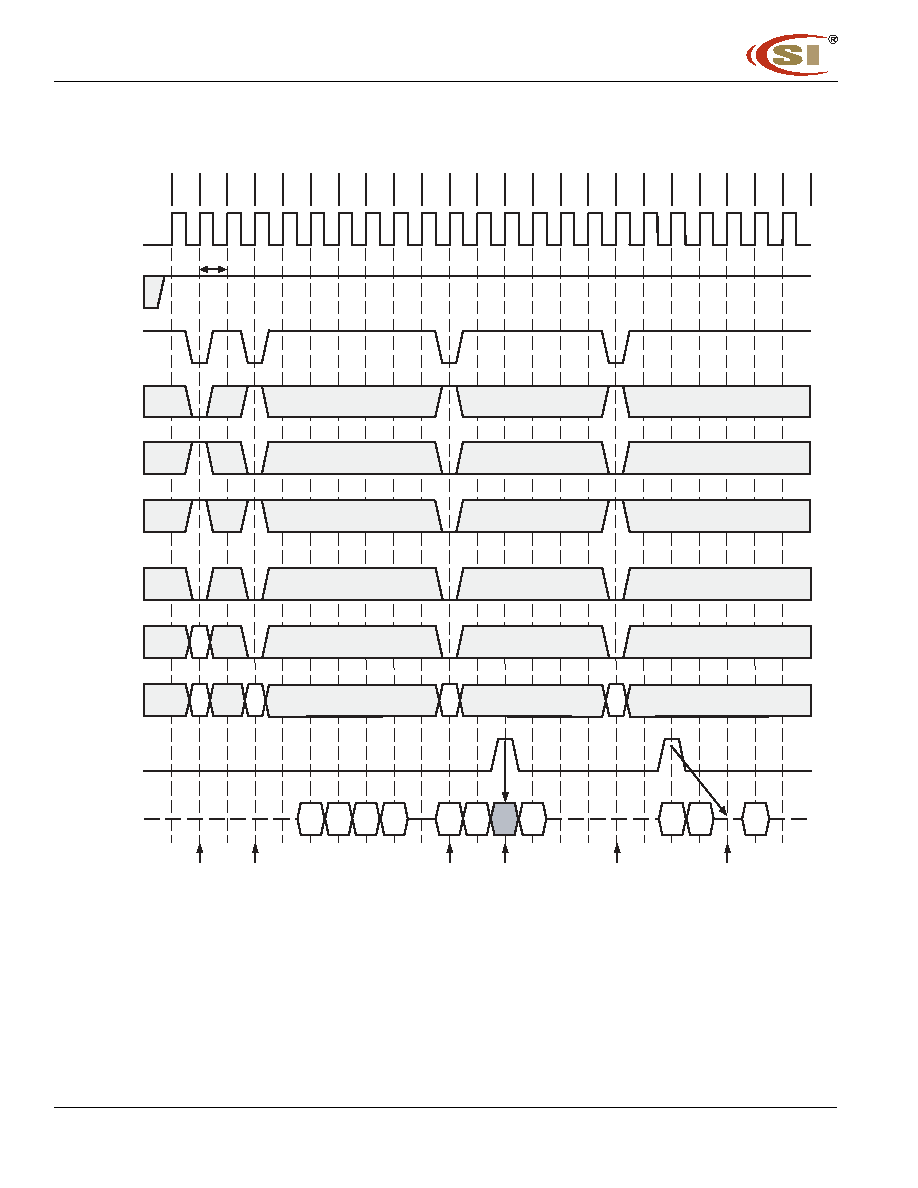
The Read command that interrupts a write burst without auto precharge function should be issued one cycle after
the clock edge in which the last data-in element is registered.In order to avoid data contention,input data must
be removed from the DQs at least one clock cycle before the first read data appears on the outputs (refer to the
following figure).Once the Read command is registered,the data inputs will be ignored and writes will not be
executed.
Write Interrupted by a Read (Burst Length =4,CAS#Latency =2,3)
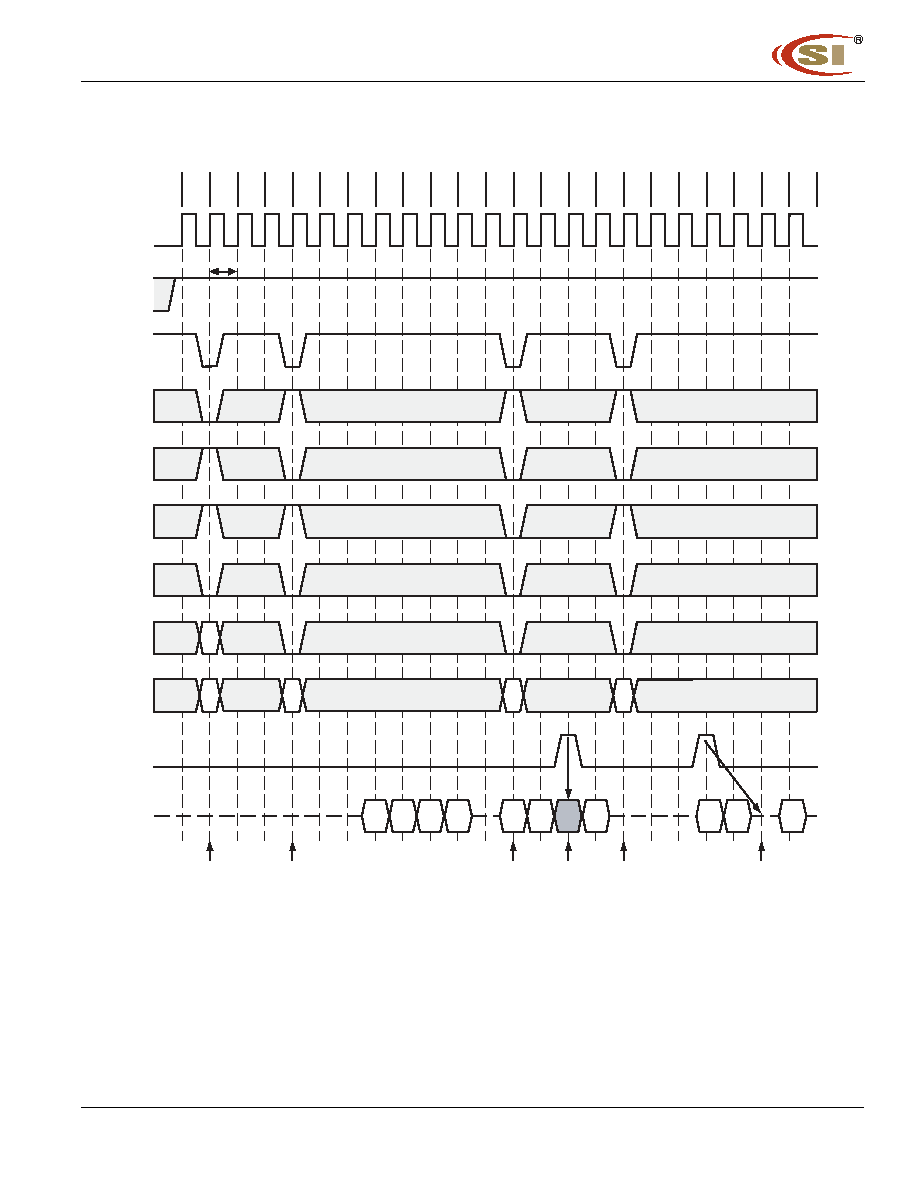
The BankPrecharge/PrechargeAll command that interrupts a write burst without the auto precharge function
should be issued m cycles after the clock edge in which the last data-in element is registered,where m equals tWR/
tCK rounded up to the next whole number.In addition,the DQM signals must be used to mask input data,starting
with the clock edge following the last data-in element and ending with the clock edge on which the BankPrecharge/
PrechargeAll command is entered (refer to the following figure).
Note:The DQMs can remain low in this example if the length of the write burst is 1 or 2.
Write to Precharge
IC42S32400
IC42S32400L
Integrated Circuit Solution Inc.
13
DR038-0C 02/01/2005
DON T CARE
CLK
DQ
D
OUT
a
T2
T1
T4
T3
T6
T5
T0
COMMAND
READ - AP
BANK n
NOP
NOP
NOP
NOP
D
OUT
a + 1
D
OUT
d
D
OUT
d + 1
NOP
T7
BANK n
CAS Latency = 3 (BANK m)
BANK m
ADDRESS
Idle
NOP
NOTE: DQM is LOW.
BANK n,
COL a
BANK m,
COL d
READ - AP
BANK m
Internal
States
t
Page Active
READ with Burst of 4
Interrupt Burst, Precharge
Page Active
READ with Burst of 4
Precharge
RP - BANK n
tRP - BANK m
CAS Latency = 3 (BANK n)
6
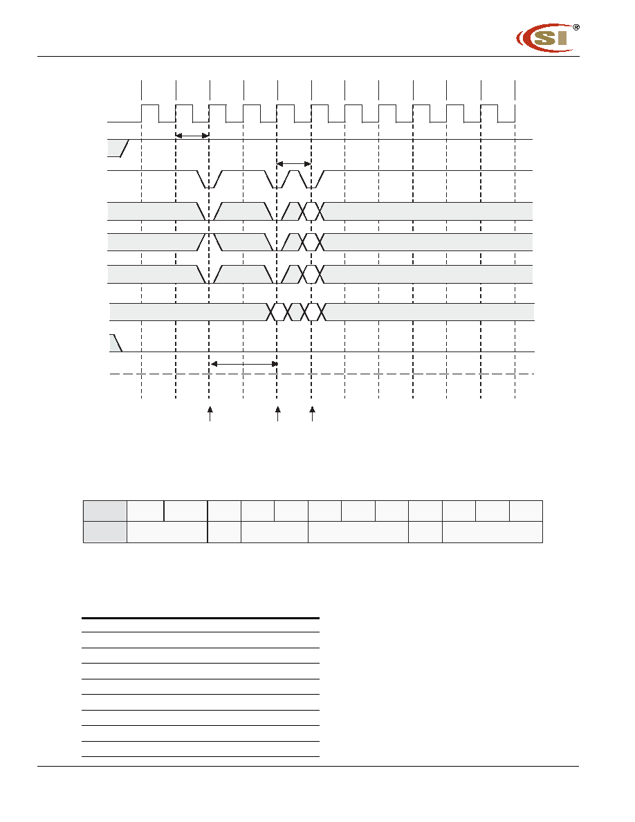
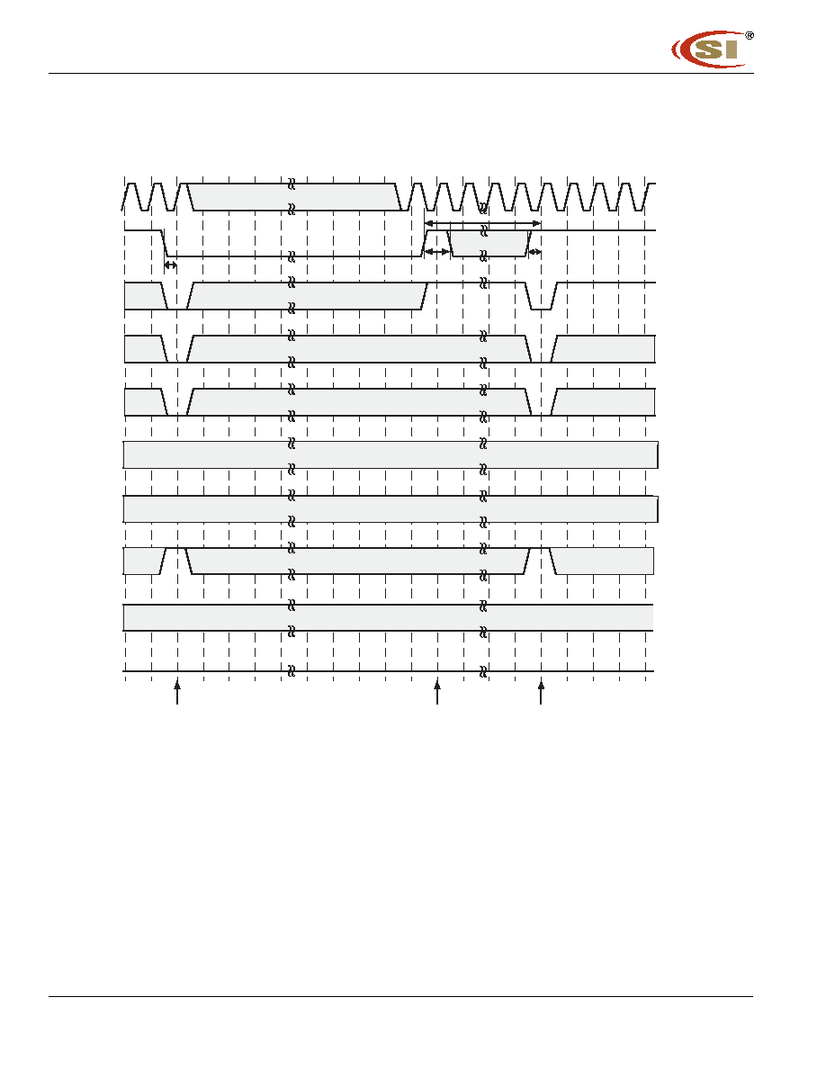
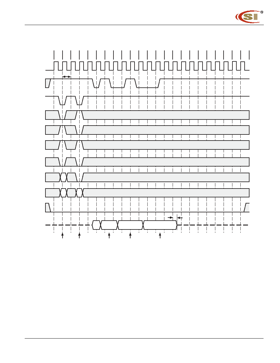
Concurrent Auto Precharge
An access command (READ or WRITE) to another bank while an access command with auto precharge enabled
is executing is not allowed by SDRAMs, unless the SDRAM supports CONCURRENT AUTO PRECHARGE.
ICSI SDRAMs support CONCURRENT AUTO PRECHARGE. Four cases where CONCURRENT AUTO
PRECHARGE occurs are defined below.
READ with Auto Precharge
� Interrupted by a READ (with or without auto precharge): A READ to bank m will interrupt a READ on bank n,
CAS latency later. The PRECHARGE to bank n will begin when the READ to bank m is regis-tered.
READ With Auto Precharge Interrupted by a READ
� Interrupted by a WRITE (with or without auto precharge): A WRITE to bank m will interrupt a READ on bank n
when registered. DQM should be used two clocks prior to the WRITE command to prevent bus contention. The
PRECHARGE to bank n will begin when the WRITE to bank m is registered.
READ With Auto Precharge Interrupted by a WRITE
CLK
DQ
D
OUT
a
T2
T1
T4
T3
T6
T5
T0
COMMAND
NOP
NOP
NOP
NOP
D
IN
d + 1
D
IN
d
D
IN
d + 2
D
IN
d + 3
NOP
T7
BANK n
BANK m
ADDRESS
Idle
NOP
DQM
NOTE: 1. DQM is HIGH at T2 to prevent D
OUT
-a+1 from contending with D
IN
-d at T4.
BANK n,
COL a
BANK m,
COL d
WRITE - AP
BANK m
Internal
States
t
Page
Active
READ with Burst of 4
Interrupt Burst, Precharge
Page Active
WRITE with Burst of 4
Write-Back
RP - BANK n
t WR - BANK m
CAS Latency = 3 (BANK n)
READ - AP
BANK n
1
DON'T CARE
IC42S32400
IC42S32400L
14
Integrated Circuit Solution Inc.
DR038-0C 02/01/2005
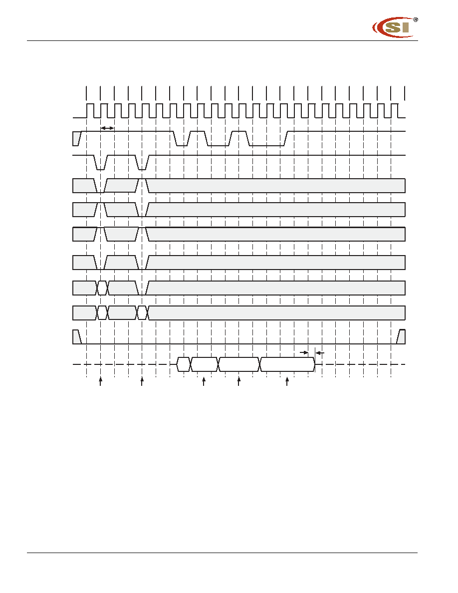
WRITE with Auto Precharge
� Interrupted by a READ (with or without auto precharge): A READ to bank m will interrupt a WRITE on bank n
when registered, with the data-out ap- pearing CAS latency later. The PRECHARGE to bank n will begin after
t WR is met, where t WR begins when the READ to bank m is registered. The last valid WRITE to bank n will
be data-in registered one clock prior to the READ to bank m.
WRITE With Auto Precharge Interrupted by a READ
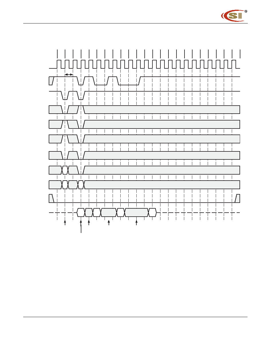
� Interrupted by a WRITE (with or without auto precharge): A WRITE to bank m will interrupt a WRITE on bank
n when registered. The PRECHARGE to bank n will begin after t WR is met, where t WR begins when the WRITE
to bank m is registered. The last valid data WRITE to bank n will be data registered one clock prior to a WRITE
to bank m.
WRITE With Auto Precharge Interrupted by a WRITE
D
IN
a
D
IN
d + 2
D
IN
d + 3
DON'T CARE
T2
T1
T4
T3
T6
T5
T0
COMMAND
T7
BANK n
NOP
D
IN
d + 1
WRITE - AP
BANK n
NOP
NOP
NOP
NOTE: 1. DQM is LOW.
BANK n,
COL a
BANK m,
COL d
WRITE - AP
BANK m
NOP
D
IN
a + 1
D
IN
a + 2
D
IN
d
Page Active
WRITE with Burst of 4
Write-Back
WR - BANK n
tRP - BANK n
t WR - BANK m
BANK m
ADDRESS
Internal
States
t
Page Active
WRITE with Burst of 4
Interrupt Burst, Write-Back
Precharge
T2
T1
T4
T3
T6
T5
T0
COMMAND
WRITE - AP
BANK n
NOP
NOP
NOP
NOP
NOTE: 1. DQM is LOW.
BANK n,
COL a
BANK m,
COL d
READ - AP
BANK m
NOP
NOP
Page Active
READ with Burst of 4
Internal
States
t
Page Active
WRITE with Burst of 4
Interrupt Burst, Write-Back
Precharge
WR - BANK n
RP - BANK n
t
tRP - BANK m
T7
BANK n
BANK m
ADDRESS
CLK
DQ
D
IN
a
D
IN
a + 1
D
OUT
d
D
OUT
d + 1
CAS Latency = 3 (BANK m)
DON'T CARE

IC42S32400
IC42S32400L
Integrated Circuit Solution Inc.
15
DR038-0C 02/01/2005
7
Mode Register Set command
(RAS#="L",CAS#="L",WE#="L",BS0,1 and A11-A0 =Register Data)
The mode register stores the data for controlling the various operating modes of SDRAM.The Mode Register Set
command programs the values of CAS#latency,Addressing Mode and Burst Length in the Mode register to make
SDRAM useful for a variety of different applications.The default values of the Mode Register after power-up are
undefined;therefore this command must be issued at the power-up sequence.The state of pins BS0,1 and
A11~A0 in the same cycle is the data written to the mode register.One clock cycle is required to complete the write
in the mode register (refer to the following figure).The contents of the mode register can be changed using the
same command and the clock cycle requirements during operation as long as all banks are in the idle state.
IC42S32400
IC42S32400L
16
Integrated Circuit Solution Inc.
DR038-0C 02/01/2005
Mode Register Set Cycle
The mode register is divided into various fields depending on functionality.
*Note:RFU (Reserved for future use)should stay 0 during MRS cycle.
�
Burst Length Field (A2~A0)
This field specifies the data length of column access using the A2~A0 pins and selects the Burst Length to be
2,4,8,or full page.
RAS#
CLK
CKE
CS#
CAS#
WE#
ADDR.
DQM
DQ
tCK2
Clock min.
Address Key
t
RP
Hi-Z
Precharge All
Mode Register
Set Command
Any
Command
T0
T2
T1
T3
T4
T5
T6
T7
T8
T9
T10
A2
A1
A0
Burst Length
0
0
0
1
0
0
1
2
0
1
0
4
0
1
1
8
1
0
0
Reserved
1
0
1
Reserved
1
1
0
Reserved
1
1
1
Full Page
Address BS0,1 A11/A10
A9
A8
A7
A6
A5
A4
A3
A2
A1
A0
Function
RFU*
WBL
Test Mode
CAS Latency
BT
Burst Length
IC42S32400
IC42S32400L
Integrated Circuit Solution Inc.
17
DR038-0C 02/01/2005
Data n
0
1
2
3
4
5
6
7
-
255
256
257
-
Column Address
n
n+1
n+2
n+3
n+4
n+5
n+6
n+7
-
n+255
n
n+1
-
2 words:
Burst Length
4 words:
8 words:
Full Page: Column address is repeated until terminated.
Data n
Column Address
Burst Length
Data
0
A7 A6 A5 A4 A3 A2 A1 A0
Data
1
A7 A6 A5 A4 A3 A2 A1 A0#
4
words
Data
2
A7 A6 A5 A4 A3 A2 A1# A0
Data
3
A7 A6 A5 A4 A3 A2 A1# A0#
8 words
Data
4
A7 A6 A5 A4 A3 A2# A1 A0
Data
5
A7 A6 A5 A4 A3 A2# A1 A0#
Data
6
A7 A6 A5 A4 A3 A2# A1# A0
Data
7
A7 A6 A5 A4 A3 A2# A1# A0#
�
Burst Type Field (A3)
The Burst Type can be one of two modes,Interleave Mode or Sequential Mode.
--Addressing Sequence of Sequential Mode
An internal column address is performed by increasing the address from the column address which is input to the
device.The internal column address is varied by the Burst Length as shown in the following table.When the value
of column address,(n +m),in the table is larger than 255,only the least significant 8 bits are effective.
�
Addressing Sequence of Interleave Mode
A column access is started in the input column address and is performed by inverting the address
bits in the sequence shown in the following table.
�
CAS#Latency Field (A6~A4)
This field specifies the number of clock cycles from the assertion of the Read command to the first
read data.The minimum whole value of CAS#Latency depends on the frequency of CLK.The
minimum whole value satisfying the following formula must be programmed into this field.
t
CAC
(min)<=CAS#Latency X t
CK
A6 A5
A4
CAS#Latency
0
0
0
Reserved
0
0
1
Reserved
0
1
0
2 clocks
0
1
1
3 clocks
1
X
X
Reserved
A3 Burst Type
0
Sequential
1
Interleave
IC42S32400
IC42S32400L
18
Integrated Circuit Solution Inc.
DR038-0C 02/01/2005
�
Test Mode field (A8~A7)
These two bits are used to enter the test mode and must be programmed to "00"in normal operation.
�
Write Burst Length (A9)
This bit is used to select the burst write length.
8
No-Operation command
(RAS#="H",CAS#="H",WE#="H")
The No-Operation command is used to perform a NOP to the SDRAM which is selected (CS#
is Low).This prevents unwanted commands from being registered during idle or wait states.
9
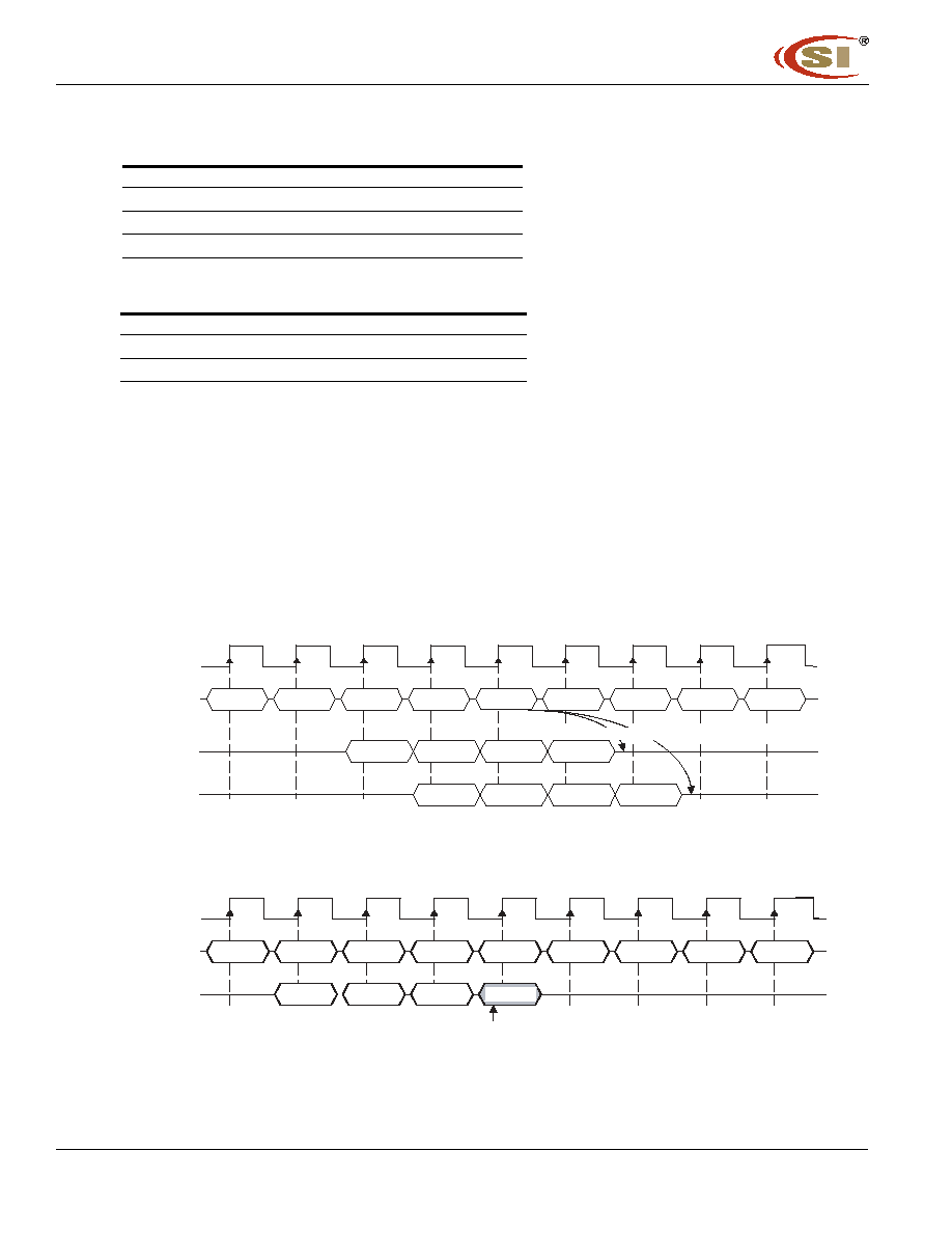
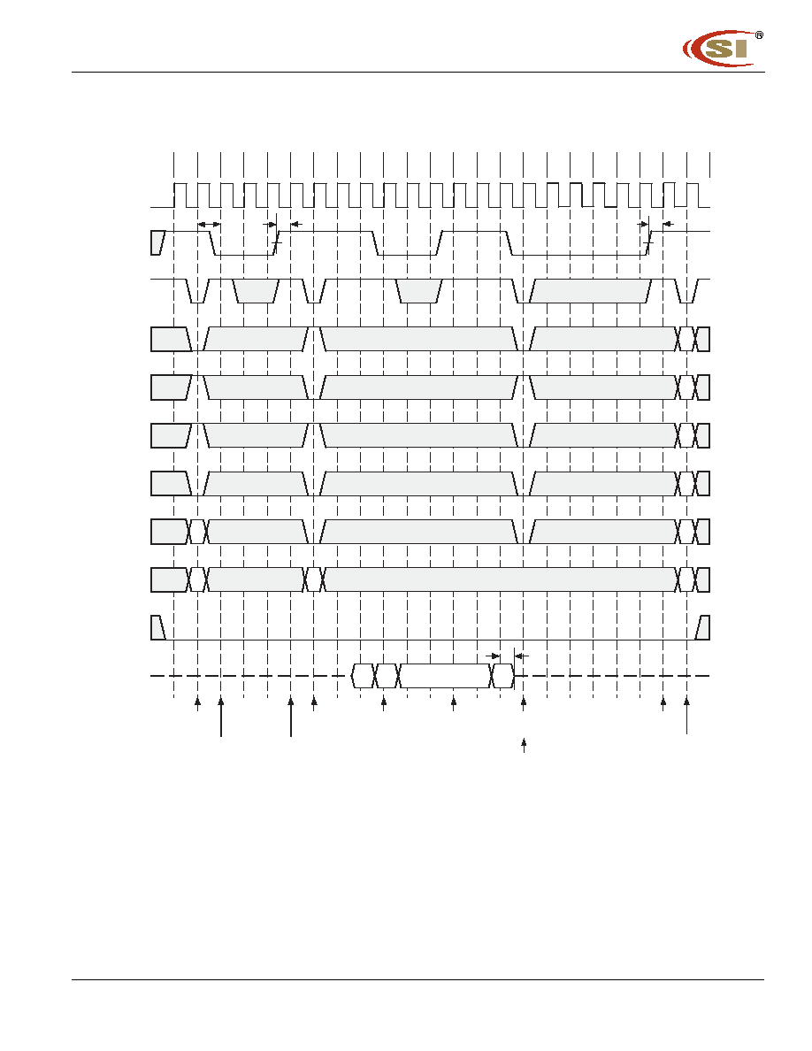
Burst Stop command
(RAS#="H",CAS#="H",WE#="L")
The Burst Stop command is used to terminate either fixed-length or full-page bursts.This
command is only effective in a read/write burst without the auto precharge function.The terminated
read burst ends after a delay equal to the CAS#latency (refer to the following figure).The
termination of a write burst is shown in the following figure.
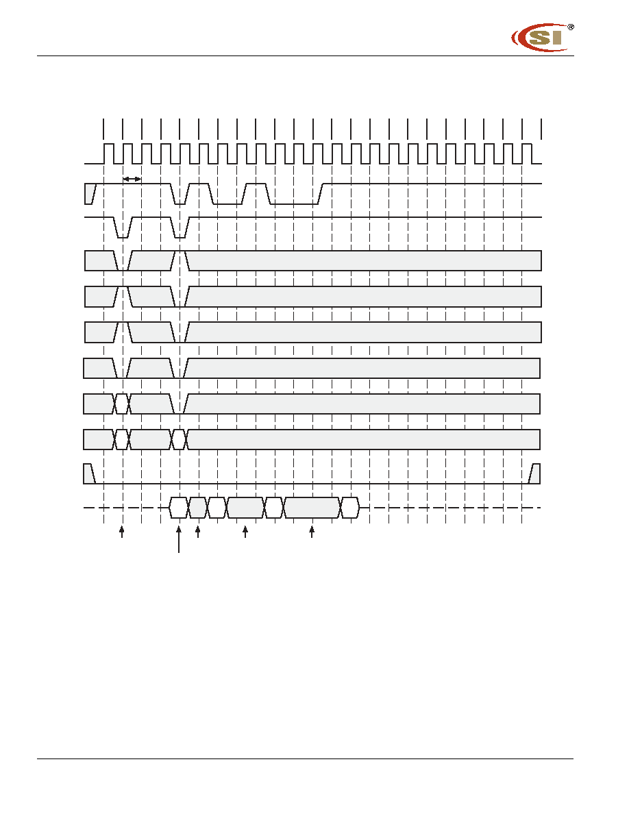
Termination of a Burst Read Operation (Burst Length > 4,CAS#Latency =2,3)
Termination of a Burst Write Operation (Burst Length =X)
CLK
COMMAND
T0
T 1
T2
T3
T4
T5
T6
T7
T8
READ A
NOP
NOP
NOP
NOP
NOP
NOP
NOP
CAS# latency=2
tCK2,DQ's
DOUT A0
DOUT A1
DOUT A2
DOUT A3
DOUT A0
DOUT A1
DOUT A2
DOUT A3
CAS# latency=3
tCK3,DQ's
The Burst ends after a delay equal to the CAS# latency.
Burst Stop
CL K
COMMAN D
T0
T 1
T2
T3
T4
T5
T6
T7
T8
NOP
WRITE A
NOP
NOP
NOP
NOP
NOP
NOP
Burst Stop
CAS# latency=2,3
DQ's
DIN A0
DIN A1
DIN A2
don't care
Input Data for the Write is masked.
A8
A7
Test Mode
0
0
normal mode
0
1
Vendor Use Only
1
X
Vendor Use Only
A9
Write Burst Length
0
Burst
1
Single Bit

IC42S32400
IC42S32400L
Integrated Circuit Solution Inc.
19
DR038-0C 02/01/2005
10
Device Deselect command (CS#="H")
The Device Deselect command disables the command decoder so that the RAS#,CAS#,WE# and Address inputs
are ignored,regardless of whether the CLK is enabled.This command is similar to the No Operation command.
11
AutoRefresh command
(RAS#="L",CAS#="L",WE#="H",CKE ="H")
The AutoRefresh command is used during normal operation of the SDRAM and is analogous to CAS#-before-
RAS#(CBR)Refresh in conventional DRAMs.This command is non-persistent,so it must be issued each time a
refresh is required.The addressing is generated by the internal refresh controller.This makes the address bits a
"don 't care"during an AutoRefresh command.The internal refresh counter increments automatically on every
auto refresh cycle to all of the rows.The refresh operation must be performed 4096 times within 64ms.The time
required to complete the auto refresh operation is specified by tRC(min.).To provide the AutoRefresh command,
all banks need to be in the idle state and the device must not be in power down mode (CKE is high in the previous
cycle).This command must be followed by NOPs until the auto refresh operation is completed.The precharge time
requirement,tRP(min),must be met before successive auto refresh operations are performed.
12
SelfRefresh Entry command
(RAS#="L",CAS#="L",WE#="H",CKE ="L")
The SelfRefresh is another refresh mode available in the SDRAM.It is the preferred refresh mode for data retention
and low power operation.Once the SelfRefresh command is registered,all the inputs to the SDRAM become "don
't care"with the exception of CKE,which must remain LOW.The refresh addressing and timing is internally
generated to reduce power consumption.The SDRAM may remain in SelfRefresh mode for an indefinite period.
The SelfRefresh mode is exited by restarting the external clock and then asserting HIGH on CKE (SelfRefresh
Exit command).
13
SelfRefresh Exit command
(CKE ="H",CS#="H"or CKE ="H",RAS#="H",CAS#="H",WE#="H")
This command is used to exit from the SelfRefresh mode.Once this command is registered, NOP or Device
Deselect commands must be issued for tRC(min.)because time is required for the completion of any bank
currently being internally refreshed.If auto refresh cycles in bursts are performed during normal operation,a burst
of 4096 auto refresh cycles should be completed just prior to entering and just after exiting the SelfRefresh mode.
14
Clock Suspend Mode Entry /PowerDown Mode Entry command (CKE ="L")
When the SDRAM is operating the burst cycle,the internal CLK is suspended(masked)from the subsequent cycle
by issuing this command (asserting CKE "LOW").The device operation is held intact while CLK is suspended.On
the other hand,when all banks are in the idle state,this command performs entry into the PowerDown mode.All
input and output buffers (except the CKE buffer)are turned off in the PowerDown mode.The device may not remain
in the Clock Suspend or PowerDown state longer than the refresh period (64ms)since the command does not
perform any refresh operations.
15
Clock Suspend Mode Exit /PowerDown Mode Exit command
When the internal CLK has been suspended,the operation of the internal CLK is einitiated from the subsequent
cycle by providing this command (asserting CKE "HIGH").When the device is in the PowerDown mode,the device
exits this mode and all disabled buffers are turned on to the active state.t
PDE
(min.)is required when the device
exits from the PowerDown mode.Any subsequent commands can be issued after one clock cycle from the end
of this command.
16
Data Write /Output Enable,Data Mask /Output Disable command (DQM ="L","H")
During a write cycle,the DQM signal functions as a Data Mask and can control every word of
the input data.During a read cycle,the DQM functions as the controller of output buffers.DQM is also used for
device selection,byte selection and bus control in a memory system.
IC42S32400
IC42S32400L
20
Integrated Circuit Solution Inc.
DR038-0C 02/01/2005
ABSOLUTE MAXIMUM RATINGS
(1)
Symbol
Parameters
Rating
Unit
V
DD
Supply Voltage (with respect to V
SS
)
�0.5 to +4.6
V
V
DDQ
Supply Voltage for Output (with respect to V
SSQ
)
�0.5 to +4.6
V
V
I
Input Voltage
(with respect to V
SS
)
�0.5 to V
DD
+0.5
V
V
O
Output Voltage
(with respect to V
SSQ
)
�1.0 to V
DDQ
+0.5
V
I
O
Short circuit output current
50
mA
P
D
Power Dissipation (
T
A
= 25 �C)
1
W
T
OPT
Operating Temperature
0 to +70
�C
T
STG
Storage Temperature
�65 to +150
�C
Notes:
1. Exposing the device to stress above those listed in Absolute Maximum Ratings could cause permanent damage. The device is not meant
to be operated under conditions outside the limits described in the operational section of this specification. Exposure to Absolute
Maximum Rating conditions for extended periods may affect device reliability.
DC RECOMMENDED OPERATING CONDITIONS
(
At T
A
= 0 to +70�C unless otherwise noted)
Symbol
Parameter
Min.
Typ.
Max.
Unit
V
DD
Supply Voltage
3.0
3.3
3.6
V
V
DDQ
Supply Voltage for DQ
3.0
3.3
3.6
V
V
IH
High Level Input Voltage (all Inputs)
2.0
--
V
DD
+ 1.2
V
V
IL
Low Level Input Voltage (all Inputs)
-1.2
--
+0.8
V
Notes:
1. All voltages are referenced to V
SS
=0V
2. V
IH
(max) for pulse width with
3ns of duration
3. V
IL
(min) for pulse width with
3ns of duration
CAPACITANCE CHARACTERISTICS
(At T
A
= 0 ~ 70�C, V
DD
= V
DDQ
= 3.3 � 0.3V, V
SS
= V
SSQ
= 0V , unless otherwise noted)
Symbol
Parameter
Min.
Max.
Unit
-6
-7/-8
C
IN
Input Capacitance, address & control pin
2.5
3.8
5.0
pF
C
CLK
I
nput Capacitance, CLK pin
2.5
3.5
4.0
pF
C
I
/
O
Data Input/Output Capacitance
4.0
6.5
6.5
pF
IC42S32400
IC42S32400L
Integrated Circuit Solution Inc.
21
DR038-0C 02/01/2005
- 6/7/8
Description/Test condition
Symbol
Max.
Unit
Note
Operating Current
t
RC
t
RC
(min), Outputs Open, Input
signal one transition per one cycle
1 bank
operation
I
CC1
140/130/130
3
Precharge Standby Current in power down mode
t
CK
= 15ns, CKE
V
IL
(max)
I
CC2P
2
Precharge Standby Current in power down mode
t
CK
=
, CKE
V
IL
(max)
I
CC2PS
2
Precharge Standby Current in non-power down mode
t
CK
= 15ns, CS#
V
IH
(min), CKE
V
IH
Input signals are changed once during 30ns.
I
CC2N
20
3
Precharge Standby Current in non-power down mode
t
CK
=
, CLK
V
IL
(max), CKE
V
IH
I
CC2NS
10
Active Standby Current in power down mode
C KE
V
IL
(max), t
CK
= 15ns
I
CC3P
7
mA
3
Active Standby Current in power down mode
CKE& CLK
V
IL
(max), t
CK
=
I
CC3PS
6
Active Standby Current in non-power down mode
CKE
V
IH
(min), CS#
V
IH
(min), t
CK
= 15ns
I
CC3N
30
Active Standby Current in non-power down mode
CKE
V
IH
(min), CLK
V
IL
(max), t
CK
=
I
CC3NS
20
Operating Current (Burst mode)
t
CK
=t
CK
(min),
Outputs Open, Multi-bank interleave
I
CC4
200/180/150
3, 4
Refresh Current
t
RC
t
RC
(min)
I
CC5
200/180/160
3
Self Refresh Current
C KE
0.2V
I
CC6
0.8 (L-Version)
2
Parameter
Description
Min.
Max.
Unit
Note
I
IL
Input Leakage Current
(0V V
IN
V
DD
, All other pins not under test = 0V )
- 5
+ 5
�A
V
OH
LVTTL Output "H" Level Voltage
( I
OUT
= -2mA )
2.4
V
V
OL
LVTTL Output "L" Level Voltage
( I
OUT
= 2mA )
0.4
V
3
3
Recommended D.C.Operating Conditions (VDD =3.3V � 0.3V,Ta =0~70 C)
IC42S32400
IC42S32400L
22
Integrated Circuit Solution Inc.
DR038-0C 02/01/2005
- 6/7/8
Symbol
A.C. Parameter
Min.
Max.
Unit
Note
t
RC
Row cycle time
(same bank)
60/70/80
9
t
RRD
Row activate to row activate delay
(different banks)
12/14/16
9
t
RCD
RAS# to CAS# delay
(same bank)
18/21/24
9
t
RP
Precharge to refresh/row activate command
(same bank)
18/21/24
9
t
RAS
Row activate to precharge time
(same bank)
42/49/56
100,000
9
t
CK2
Clock cycle time
CL* = 2
- / - /10
t
CK3
CL* = 3
6/7/8
ns
t
AC2
Access time from CLK
CL* = 2
- / - /8
9
t
AC3
(positive edge)
CL* = 3
5.5/5.5/6
t
OH
Data output hold time
2/2.5/2.5
9
t
CH
Clock high time
2/3/3
10
t
CL
Clock low time
2/3/3
10
t
IS
Data/Address/Control Input set-up time
1.5/1.75/2
10
t
IH
Data/Address/Control Input hold time
1
10
t
LZ
Data output low impedance
1
9
t
HZ
Data output high impedance
5.5/5.5/6
8
* CL is CAS# Latency.
t
DAL
Input data to active/refresh command
2CLK+t
RP
delay time (During Auto-precharge)
t
SRX
Exit self refresh and active command
70
t
RFC
Auto refresh Period
t
REF
Refresh cycle time(4096)
64
60/70/80
ms
t
WR
Write Recovery Time
2
t
CCD
CAS# to CAS# Delay time
CLK
t
MRS
Mode Register Set cycle time
2
t
PDE
CKE to clock enable or power down exit
setup mode
1
1
Electrical Characteristics and Recommended A.C.Operating Conditions
(VDD =3.3V � 0.3V,Ta =0~70 C)(Note:5,6,7,8)
Note:
1. Stress greater than those listed under "Absolute Maximum Ratings"may cause permanent damage to the device.
2. All voltages are referenced to VSS.
3. These parameters depend on the cycle rate and these values are measured by the cycle rate under the minimum value of
tCK and tRC.Input signals are changed one time during tCK.
4. These parameters depend on the output loading.Specified values are obtained with the output open.
5. Power-up sequence is described in Note 11.
IC42S32400
IC42S32400L
Integrated Circuit Solution Inc.
23
DR038-0C 02/01/2005
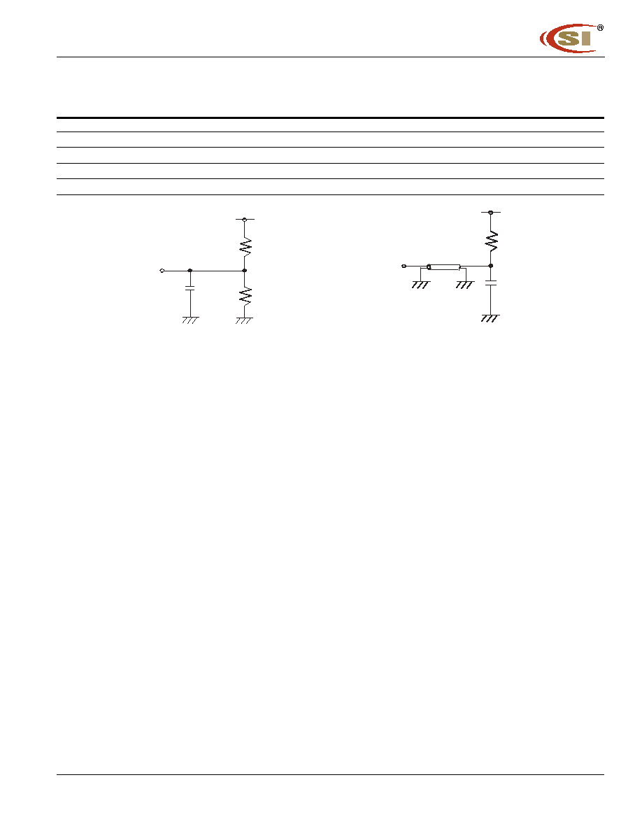
6.A.C.Test Conditions
LVTTL Interface
Reference Level of Output Signals
1.4V /1.4V
Output Load
Reference to the Under Output Load (B)
Input Signal Levels
2.4V /0.4V
Transition Time (Rise and Fall)of Input Signals
1ns
Reference Level of Input Signals
1.4V
3.3V
1.2k
870
30pF
Output
LVTTL D.C. Test Load (A)
1.4V
50
Output
30pF
Z0=
50
LVTTL A.C. Test Load (B)
7.
Transition times are measured between VIH and VIL.Transition(rise and fall)of input signals are in a fixed slope
(1 ns).
8.
t
HZ
defines the time in which the outputs achieve the open circuit condition and are not at reference levels.
9.
If clock rising time is longer than 1 ns,(t
R
/2 -0.5)ns should be added to the parameter.
10. Assumed input rise and fall time t
T
(t
R
&t
F
)=1 ns
If t
R
or t
F
is longer than 1 ns,transient time compensation should be considered,i.e.,[(tr +tf)/2 -1 ]ns
should be added to the parameter.
11. Power up Sequence
Power up must be performed in the following sequence.
1) Power must be applied to V
DD
and V
DDQ
(simultaneously)when all input signals are held "NOP"state
and both CKE ="H"and DQM ="H."The CLK signals must be started at the same
time.
2) After power-up,a pause of 200
�
seconds minimum is required.Then,it is recom
mended that DQM is held "HIGH"(V
DD
levels)to ensure DQ output is in high
impedance.
3) All banks must be precharged.
4) Mode Register Set command must be asserted to initialize the Mode register.
5) A minimum of 2 Auto-Refresh dummy cycles must be required to stabilize the internal circuitry of the device.
IC42S32400
IC42S32400L
24
Integrated Circuit Solution Inc.
DR038-0C 02/01/2005
Timing Waveforms
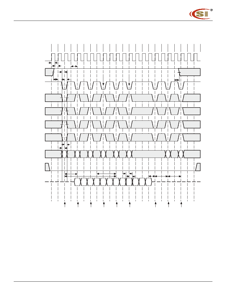
Figure 1.AC Parameters for Write Timing (Burst Length=4,CAS#Latency=2)
-5 ,
, -7 ,
x
x
BS0,1
t
CH
t
CL
t
CK2
t
IS
t
IS
t
IH
Begin Auto Precharge
Bank A
Begin Auto Precharge
Bank B
t
IS
t
IH
t
IS
RBx
CAx
RBx
CBx
RAy
CAy
RAz
RBy
t
RCD
t
DAL
t
RC
t
IS
t
IH
t
WR
t
RP
t
RRD
Ax0 Ax1 Ax2
Ax3 Bx0 Bx1 Bx2 Bx3 Ay0 Ay1 Ay2 Ay3
Activate
Command
Bank A
Write with
Auto Precharge
Command
Bank A
Activate
Command
Bank B
Write with
Auto Precharge
Command
Bank B
Activate
Command
Bank A
Write
Command
Bank A
Precharge
Command
Bank A
Activate
Command
Bank A
Activate
Command
Bank B
CLK
CKE
CS#
RAS#
CAS#
WE#
ADDR.
DQM
DQ
Hi-Z
T0
T2
T1
T3 T4 T5 T6 T7
T9
T8
T12
T11
T10
T14
T13
T15 T16 T17 T18 T19
T21
T20
T22
IC42S32400
IC42S32400L
Integrated Circuit Solution Inc.
25
DR038-0C 02/01/2005
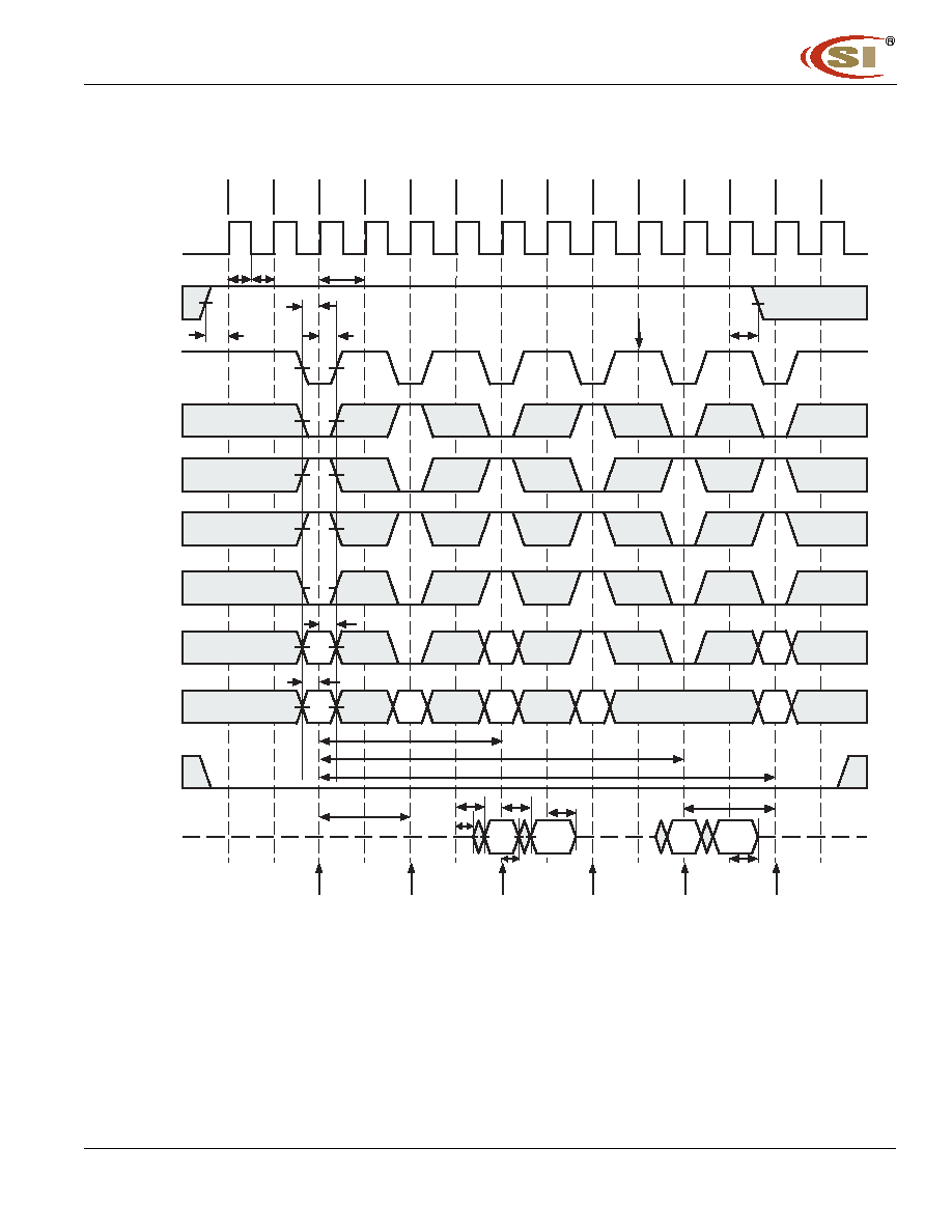
Figure 2.AC Parameters for Read Timing (Burst Length=2,CAS#Latency=2)
A10
A0-A9
DQ
t
CH
t
CL
t
CK2
t
IS
t
IS
t
IH
Begin AutoPrecharge
Bank B
t
IH
t
IH
t
IS
RAx
RAx
CAx
RBx
RBx
CBx
RAy
RAy
t
RRD
t
RAS
t
RC
t
RCD
t
AC2
t
LZ
t
OH
t
HZ
Ax0
Ax1
Bx0
Bx1
t
RP
Activate
Command
Bank A
Read
Command
Bank A
Activate
Command
Bank B
Read with
Auto Precharge
Command
Bank B
Precharge
Command
Bank A
Activate
Command
Bank A
Hi-Z
t
AC2
t
HZ
T0
T2
T1
T3
T4
T5
T6
T7
T9
T8
T12
T11
T10
T13
BS0,1
CLK
CKE
CS#
RAS#
CAS#
WE#
DQM
IC42S32400
IC42S32400L
26
Integrated Circuit Solution Inc.
DR038-0C 02/01/2005
A10
A0-A9
DQM
DQ
t
CK2
RAx
RAx
CAx
t
RP
t
RC
Ax0
Ax1
Ax2
Ax3
Precharge All
Command
Auto Refresh
Command
Auto Refresh
Command
Activate
Command
Bank A
Read
Command
Bank A
t
RC
T0
T2
T1
T3 T4 T5 T6 T7
T9
T8
T12
T11
T10
T14
T13
T15 T16 T17 T18 T19
T21
T20
T22
BS0,1
CLK
CKE
CS#
RAS#
CAS#
WE#
DQ
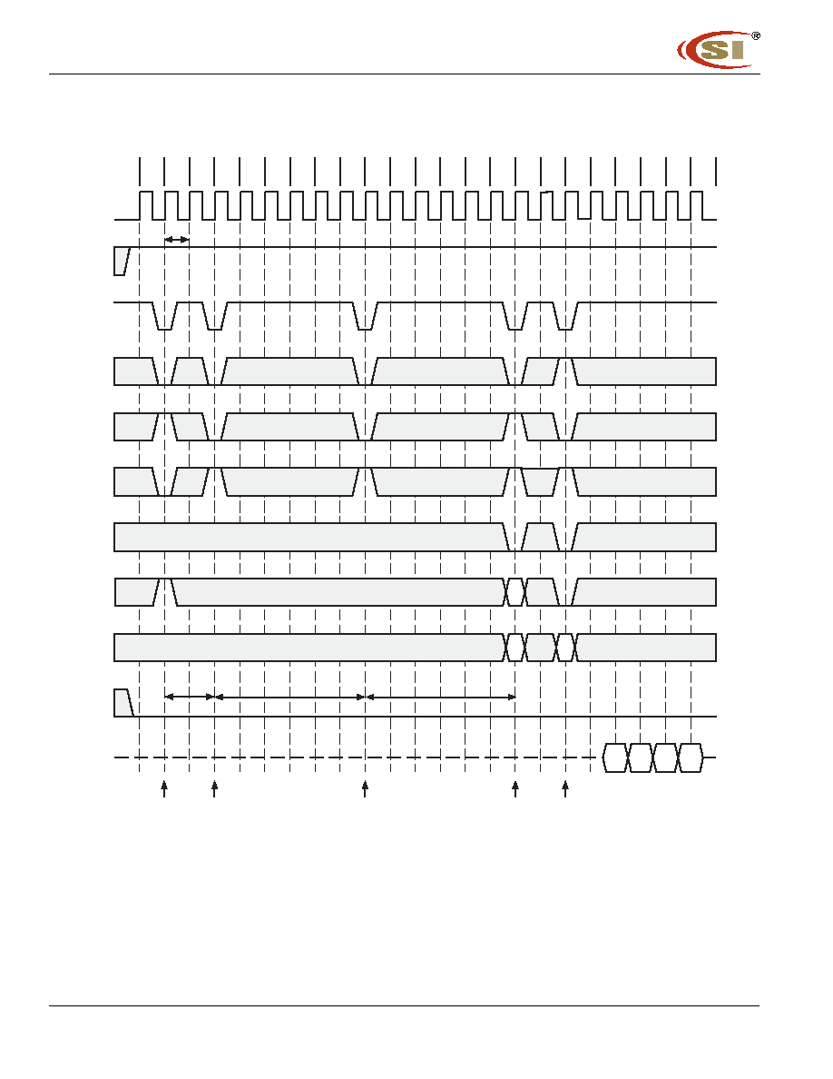
Figure 3.Auto Refresh (CBR)(Burst Length=4,CAS#Latency=2)
IC42S32400
IC42S32400L
Integrated Circuit Solution Inc.
27
DR038-0C 02/01/2005
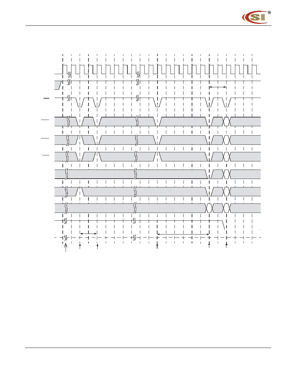
Figure 4.Power on Sequene and Auto Refresh (CBR)
T0 T1 T2 T3 T4 T5 T6 T7 T8 T9 T10 T11 T12 T13 T14 T15 T16 T17 T18 T19 T20 T21 T22
CLK
CKE
CS
RAS
CAS
WE
A10
ADD
DQM
DQ
High level
is required
Minimum of 2 Refresh Cycles are required
t
MRS
t
RP
High Level is Necessary
t
RC
Address Key
Inputs
be stable
for 200us
Precharge
All Banks
must
Command
1st Auto
Command
Refresh
2nd Auto
Refresh
Command
Mode
Set Command
Command
Register
Hi-Z
BS0, 1
IC42S32400
IC42S32400L
28
Integrated Circuit Solution Inc.
DR038-0C 02/01/2005
Figure 5.Self Refresh Entry &Exit Cycle
Note:To Enter SelfRefresh Mode
1. CS#,RAS#&CAS#with CKE should be low at the same clock cycle.
2. After 1 clock cycle,all the inputs including the system clock can be don 't care except for CKE.
3. The device remains in SelfRefresh mode as long as CKE stays "low".
Once the device enters SelfRefresh mode,minimum tRAS is required before exit from SelfRefresh.
To Exit SelfRefresh Mode
4. System clock restart and be stable before returning CKE high.
5. Enable CKE and CKE should be set high for minimum time of tSRX.
6. CS#starts from high.
7. Minimum tRC is required after CKE going high to complete SelfRefresh exit.
8. 4096 cycles of burst AutoRefresh is required before SelfRefresh entry and after SelfRefresh exit if the system uses burst refresh.
CLK
CKE
CS#
RAS#
CAS#
BS0,1
A0-A9
WE#
DQM
DQ
*Note 1
*Note 2
t
IS
*Note 3
*Note 4
t
RC(min) *Note 7
*Note 5
*Note 6
*Note 8
*Note 8
Hi-Z
Hi-Z
SelfRefresh Enter
SelfRefresh Exit
Auto Refresh
t
SRX
t
PDE
T0
T2
T1
T3
T4
T5
T6
T7
T9
T8
T12
T11
T10
T14
T13
T15
T16
T17
T18
T19
IC42S32400
IC42S32400L
Integrated Circuit Solution Inc.
29
DR038-0C 02/01/2005
Figure 6.2.Clock Suspension During Burst Read (Using CKE)
(Burst Length=4,CAS#Latency=2)
T0 T 1 T2 T3 T4 T5 T6 T7 T8 T9 T10 T 11 T12 T13 T14 T15 T16 T17 T18 T19 T20 T21 T22
t
CK2
RAx
RAx
CAx
Hi-Z
Ax0
Ax1
Ax2
Ax3
Activate
Command
Bank A
Read
Command
Bank A
Clock Suspend
1 Cycle
t
HZ
CLK
CKE
CS#
RAS#
CAS#
WE#
BS0,1
A10
A0-A9
DQM
DQ
Clock Suspend
2 Cycle
Clock Suspend
3 Cycle
Note:CKE to CLK disable/enable =1 clock
IC42S32400
IC42S32400L
30
Integrated Circuit Solution Inc.
DR038-0C 02/01/2005
Figure 6.3.Clock Suspension During Burst Read (Using CKE)
(Burst Length=4,CAS#Latency=3)
Note:CKE to CLK disable/enable =1 clock
T0 T 1
T3 T4 T5 T6 T7 T8 T9 T10 T 11 T12 T13 T14 T15 T16 T17 T18 T19 T20 T21 T22
t
CK3
RAx
RAx
CAx
Hi-Z
Ax0
Ax1
Ax2
Ax3
t
HZ
T 2
Clock Suspend
1 Cycle
Clock Suspend
2 Cycle
Clock Suspend
3 Cycle
Activate
Command
Bank A
Read
Command
Bank A
CLK
CKE
CS#
RAS#
CAS#
WE#
BS0,1
A10
A0-A9
DQM
DQ Hi-Z
IC42S32400
IC42S32400L
Integrated Circuit Solution Inc.
31
DR038-0C 02/01/2005
T0 T 1 T2 T3 T4 T5 T6 T7 T8 T9 T10 T 11 T12 T13 T14 T15 T16 T17 T18 T19 T20 T21 T22
t
CK2
RAx
RAx
CAx
DAx0
DAx1
DAx2
DAx3
CLK
CKE
CS#
RAS#
CAS#
WE#
BS0,1
A10
A0-A9
DQM
DQ
Hi-Z
Activate
Command
Bank A
Write
Command
Bank A
Clock Suspend
1 Cycle
Clock Suspend
2 Cycle
Clock Suspend
3 Cycle
Figure 7.2.Clock Suspension During Burst Write (Using CKE)
(Burst Length=4,CAS#Latency=2)
Note:CKE to CLK disable/enable =1 clock
IC42S32400
IC42S32400L
32
Integrated Circuit Solution Inc.
DR038-0C 02/01/2005
Figure 7.3.Clock Suspension During Burst Write (Using CKE)
(Burst Length=4,CAS#Latency=3)
Note:CKE to CLK disable/enable =1 clock
T0 T 1 T2 T3 T4 T5 T6 T7 T8 T9 T10 T 11 T12 T13 T14 T15 T16 T17 T18 T19 T20 T21 T22
DAx0
DAx1
DAx2
DAx3
t
CK3
RAx
RAx
CAx
CLK
CKE
CS#
RAS#
CAS#
WE#
BS0,1
A10
A0-A9
DQM
DQ Hi-Z
Activate
Command
Bank A
Clock Suspend
1 Cycle
Clock Suspend
2 Cycle
Clock Suspend
3 Cycle
Write
Command
Bank A
IC42S32400
IC42S32400L
Integrated Circuit Solution Inc.
33
DR038-0C 02/01/2005
T0 T 1 T2 T3 T4 T5 T6 T7 T8 T9 T10 T 11 T12 T13 T14 T15 T16 T17 T18 T19 T20 T21 T22
t
CK2
t
IS
t
PDE
RAx
RAx
CAx
t
HZ
Ax3
Ax2
Ax1
Ax0
Power Down
Mode Entry
Power Down
Mode Entry
Mode Exit
Clock Mask
Start
STANDBY
Any
Valid
ACTIVE
STANDBY
CLK
CKE
CS#
RAS#
CAS#
WE#
BS0,1
A10
A0-A9
DQM
DQ
Hi-Z
Activate
Command
Bank A
Read
Command
Bank A
Power Down
Mode Exit
Power Down
Clock Mask
End
Precharge
Command
Bank A
PRECHARGE
Command
Figure 8.Power Down Mode and Clock Mask (Burst Lenght=4,
CAS#Latency=2)
IC42S32400
IC42S32400L
34
Integrated Circuit Solution Inc.
DR038-0C 02/01/2005
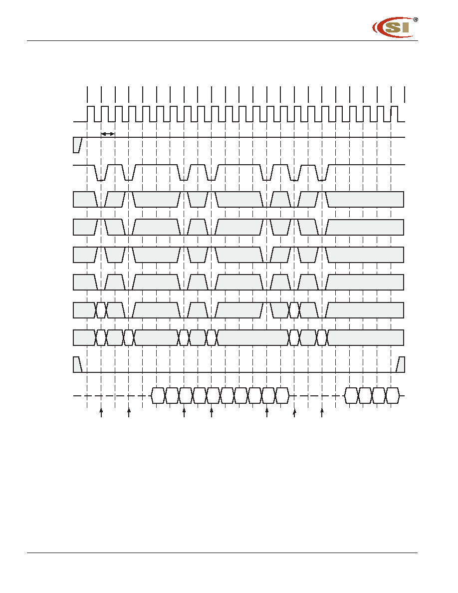
Figure 9.2.Random Column Read (Page within same Bank)
(Burst Length=4,CAS#Latency=2)
T0 T 1 T2 T3 T4 T5 T6 T7 T8 T9 T10 T 11 T12 T13 T14 T15 T16 T17 T18 T19 T20 T21 T22
t
CK2
Aw0 Aw1 Aw2 Aw3 Ax0
Ax1 Ay0
Ay1
Ay2
Ay3
RAw
RAw
CAw
CAx
CAy
CAz
Az0
Az1 Az2
Az3
Activate
RAz
RAz
CLK
CKE
CS#
RAS#
CAS#
WE#
BA0,1
A10
A0-A9
DQM
DQ Hi-Z
Activate
Command
Bank A
Read
Command
Bank A
Precharge
Command
Bank A
Read
Command
Bank A
Command
Bank A
Read
Command
Bank A
Read
Command
Bank A
IC42S32400
IC42S32400L
Integrated Circuit Solution Inc.
35
DR038-0C 02/01/2005
Figure 9.3.Random Column Read (Page within same Bank)
(Burst Length=4,CAS#Latency=3)
T0 T 1 T2 T3 T4 T5 T6 T7 T8 T9 T10 T 11 T12 T13 T14 T15 T16 T17 T18 T19 T20 T21 T22
t
CK3
Aw0 Aw1 Aw2 Aw3 Ax0 Ax1 Ay0
Ay1
Ay2
Ay3
RAw
RAw
CAw
CAx
CAy
CAz
RAz
RAz
Az0
CLK
CKE
CS#
RAS#
CAS#
WE#
BS0,1
A10
A0-A9
DQM
DQ
Hi-Z
Activate
Command
Bank A
Activate
Command
Bank A
Read
Command
Bank A
Read
Command
Bank A
Read
Command
Bank A
Read
Command
Bank A
Precharge
Command
Bank A
IC42S32400
IC42S32400L
36
Integrated Circuit Solution Inc.
DR038-0C 02/01/2005
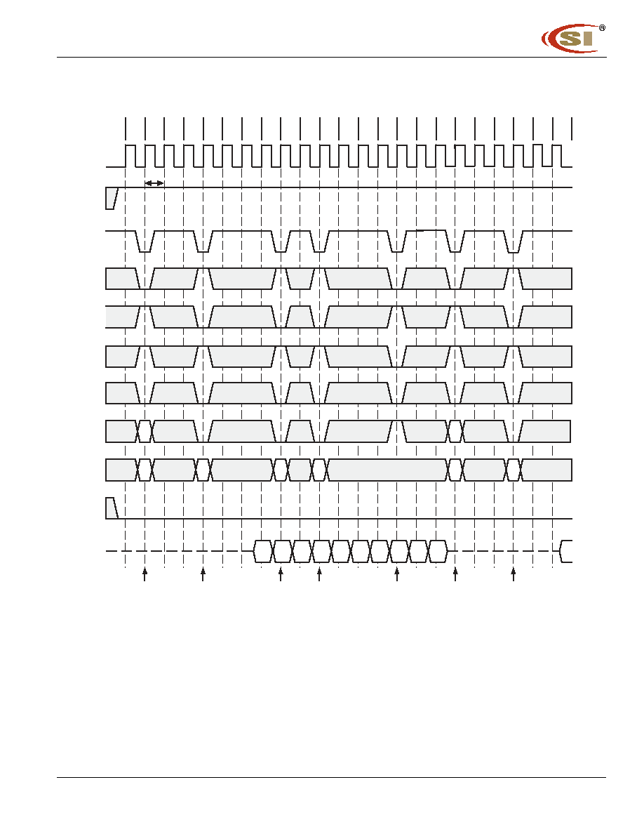
Figure 10.2.Random Column Write (Page within same Bank)
(Burst Length=4,CAS#Latency=2)
T0 T 1 T2 T3 T4 T5 T6 T7 T8 T9 T10 T 11 T12 T13 T14 T15 T16 T17 T18 T19 T20 T21 T22
t
CK2
DBw0
DBx0 DBx1 DBy0
RBw
CBw
CBx
CBy
CBz
RBz
RBz
RBw
DBw1 DBw2 DBw3
DBy1 DBy2 DBy3
DBz0 DBz1 DBz2 DBz3
CLK
CKE
CS#
RAS#
CAS#
WE#
BS0,1
A10
A0-A9
DQM
DQ
Hi-Z
Write
Command
Bank A
Write
Command
Bank B
Write
Command
Bank B
Write
Command
Bank B
Activate
Command
Bank A
Activate
Command
Bank B
Precharge
Command
Bank B
IC42S32400
IC42S32400L
Integrated Circuit Solution Inc.
37
DR038-0C 02/01/2005
Figure 10.3.Random Column Write (Page within same Bank)
(Burst Length=4,CAS#Latency=3)
T0 T 1 T2 T3 T4 T5 T6 T7 T8 T9 T10 T 11 T12 T13 T14 T15 T16 T17 T18 T19 T20 T21 T22
t
CK3
DBw0
DBx0 DBx1
RBw
CBw
CBx
CBy
CBz
DBz0
RBz
RBz
RBw
DBz1 DBz2
DBw1 DBw2 DBw3
DBy0 DBy1 DBy2 DBy3
CLK
CKE
CS#
RAS#
CAS#
WE#
BS0,1
A10
A0-A9
DQM
DQ
Hi-Z
Write
Command
Bank A
Write
Command
Bank B
Write
Command
Bank B
Write
Command
Bank B
Activate
Command
Bank A
Activate
Command
Bank B
Precharge
Command
Bank B
IC42S32400
IC42S32400L
38
Integrated Circuit Solution Inc.
DR038-0C 02/01/2005
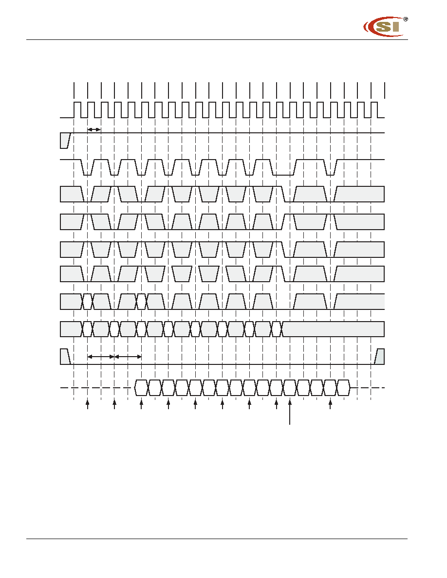
Figure 11.3.Random Row Read (Interleaving Banks)
(Burst Length=8,CAS#Latency=3)
T0 T 1 T2 T3 T4 T5 T6 T7 T8 T9 T10 T 11 T12 T13 T14 T15 T16 T17 T18 T19 T20 T21 T22
t
CK3
Bx0
Bx1 Bx2
Bx3
Bx4
Bx5 Bx6 Bx7
Ax0 Ax1
RBx
RBx
RBy
CBy
High
RAx
Ax7 By0
Ax2
Ax3
Ax4 Ax5
Ax6
CBx
CAx
RAx
RBy
t
RCD
t
AC3
t
RP
CLK
CKE
CS#
RAS#
CAS#
WE#
BS0,1
A10
A0-A9
DQM
DQ
Hi-Z
Activate
Command
Bank A
Read
Command
Bank A
Precharge
Command
Bank A
Activate
Command
Bank B
Activate
Command
Bank B
Read
Command
Bank B
Read
Command
Bank B
Precharge
Command
Bank B
IC42S32400
IC42S32400L
Integrated Circuit Solution Inc.
39
DR038-0C 02/01/2005
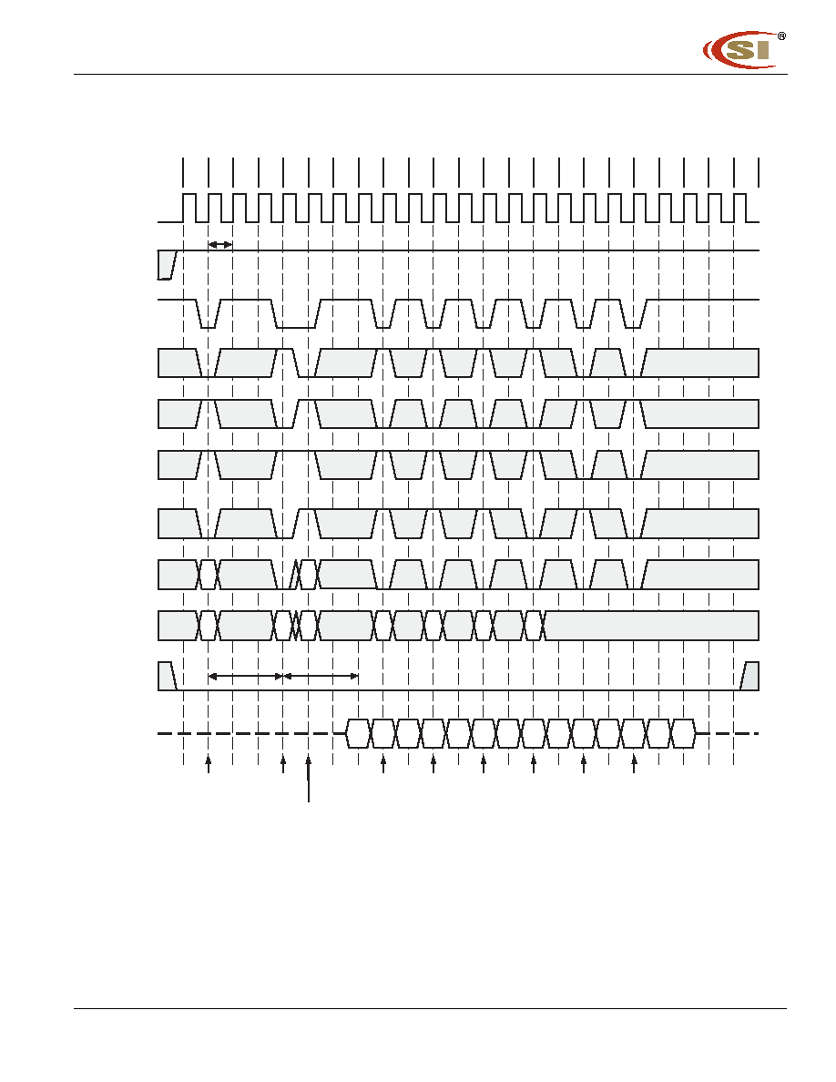
Figure 12.1.Random Row Write (Interleaving Banks)
(Burst Length=8,CAS#Latency=1)
T0 T 1 T2 T3 T4 T5 T6 T7 T8 T9 T10 T 11 T12 T13 T14 T15 T16 T17 T18 T19 T20 T21 T22
t
CK1
DAx0 DAx1 DAx2 DAx3 DAx4 DAx5 DAx6 DAx7 DBx0 DBx1
RAx
RAx
RAy
CAy
RBx
DBx7
DAy3
DBx2 DBx3 DBx4 DBx5 DBx6
CAx
RBx
RAy
t
RCD
CBx
DAy0 DAy1 DAy2
t
RP
t
WR
CLK
CKE
CS#
RAS#
CAS#
WE#
BS0,1
A10
A0-A9
DQM
DQ
Hi-Z
Write
Command
Bank A
Write
Command
Bank A
Activate
Command
Bank A
Activate
Command
Bank A
Precharge
Command
Bank A
Write
Command
Bank B
Activate
Command
Bank B
Precharge
Command
Bank B
High
IC42S32400
IC42S32400L
40
Integrated Circuit Solution Inc.
DR038-0C 02/01/2005
T0 T 1 T2 T3 T4 T5 T6 T7 T8 T9 T10 T 11 T12 T13 T14 T15 T16 T17 T18 T19 T20 T21 T22
t
CK2
DAx0 DAx1 DAx2 DAx3 DAx4 DAx5 DAx6 DAx7 DBx0 DBx1
RAx
RAx
RAy
CAy
RBx
DBx7
DBx2 DBx3 DBx4 DBx5 DBx6
CAx
CBx
RBx
RAy
t
RCD
DAy3
DAy0 DAy1 DAy2
DAy4
t
WR*
t
RP
t
WR*
* t
WR
> t
WR
(min.)
CLK
CKE
CS#
RAS#
CAS#
WE#
BS0,1
A10
A0-A9
DQM
DQ
Hi-Z
Write
Command
Bank A
Write
Command
Bank A
Activate
Command
Bank A
Activate
Command
Bank A
Precharge
Command
Bank A
Write
Command
Bank B
Activate
Command
Bank B
Precharge
Command
Bank B
High
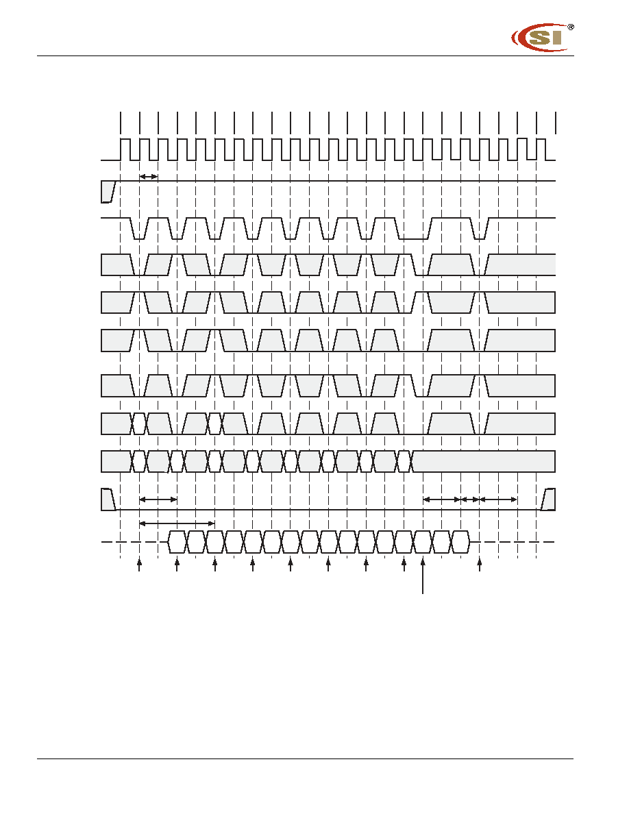
Figure 12.2.Random Row Write (Interleaving Banks)
(Burst Length=8,CAS#Latency=2)
IC42S32400
IC42S32400L
Integrated Circuit Solution Inc.
41
DR038-0C 02/01/2005
Figure 12.3.Random Row Write (Interleaving Banks)
(Burst Length=8,CAS#Latency=3)
T0 T 1 T2 T3 T4 T5 T6 T7 T8 T9 T10 T 11 T12 T13 T14 T15 T16 T17 T18 T19 T20 T21 T22
t
CK3
DAx0 DAx1 DAx2 DAx3 DAx4 DAx5 DAx6 DAx7 DBx0 DBx1
RAx
RAx
RAy
CAy
RBx
DBx7
DBx2 DBx3 DBx4 DBx5 DBx6
CAx
CBx
RBx
RAy
t
RCD
DAy3
DAy0 DAy1 DAy2
t
WR*
t
RP
t
WR*
* t
WR
> t
WR
(min.)
CLK
CKE
CS#
RAS#
CAS#
WE#
BS0,1
A10
A0-A9
DQM
DQ
Hi-Z
Write
Command
Bank A
Write
Command
Bank A
Activate
Command
Bank A
Activate
Command
Bank A
Precharge
Command
Bank A
Write
Command
Bank B
Activate
Command
Bank B
Precharge
Command
Bank B
High
IC42S32400
IC42S32400L
42
Integrated Circuit Solution Inc.
DR038-0C 02/01/2005
T0 T 1 T2 T3 T4 T5 T6 T7 T8 T9 T10 T 11 T12 T13 T14 T15 T16 T17 T18 T19 T20 T21 T22
t
CK2
Ax0
Ax1
Ax2 Ax3
DAy0 DAy1
Az3
DAy3
Az0
Az1
RAx
RAx
CAx
CAy
CAz
CLK
CKE
CS#
RAS#
CAS#
WE#
BS0,1
A10
A0-A9
DQM
DQ
Hi-Z
Write
Command
Bank A
Activate
Command
Bank A
Read
Command
Bank A
Read
Command
Bank A
The Write Data
is Masked with a
Zero Clock
Latency
The Read Data
is Masked with a
Two Clock
Latency
Figure 13.2.Read and Write Cycle (Burst Length=4,CAS#Latency=2)
IC42S32400
IC42S32400L
Integrated Circuit Solution Inc.
43
DR038-0C 02/01/2005
Figure 13.3.Read and Write Cycle (Burst Length=4,CAS#Latency=3)
T0 T 1 T2 T3 T4 T5 T6 T7 T8 T9 T10 T 11 T12 T13 T14 T15 T16 T17 T18 T19 T20 T21 T22
t
CK3
Ax0
Ax1 Ax2 Ax3
DAy0 DAy1
Az3
DAy3
Az0
Az1
RAx
RAx
CAx
CAy
CAz
CLK
CKE
CS#
RAS#
CAS#
WE#
BS0,1
A10
A0-A9
DQM
DQ
Hi-Z
Write
Command
Bank A
Activate
Command
Bank A
Read
Command
Bank A
Read
Command
Bank A
The Write Data
is Masked with a
Zero Clock
Latency
The Read Data
is Masked with a
Two Clock
Latency
IC42S32400
IC42S32400L
44
Integrated Circuit Solution Inc.
DR038-0C 02/01/2005
T0 T 1 T2 T3 T4 T5 T6 T7 T8 T9 T10 T 11 T12 T13 T14 T15 T16 T17 T18 T19 T20 T21 T22
t
CK2
Bw0 Bw1 Bx0
Bx1
By1
Ay0
Bz0
RAx
RAx
Ax0
Ax1 Ax2 Ax3
By0
Ay1
Bz1 Bz2
Bz3
t
RCD
t
AC2
CAy
RAx
RAx
CBw
CBx
CBy
CAy
CBz
CLK
CKE
CS#
RAS#
CAS#
WE#
BS0,1
A10
A0-A9
DQM
DQ
Hi-Z
Activate
Command
Bank A
Read
Command
Bank A
Read
Command
Bank A
Precharge
Command
Bank A
Activate
Command
Bank B
Read
Command
Bank B
Read
Command
Bank B
Read
Command
Bank B
Read
Command
Bank B
Precharge
Command
Bank B
Figure 14.2.Interleaving Column Read Cycle (Burst Length=4,CAS#Latency=2)
IC42S32400
IC42S32400L
Integrated Circuit Solution Inc.
45
DR038-0C 02/01/2005
T0 T 1 T2 T3 T4 T5 T6 T7 T8 T9 T10 T 11 T12 T13 T14 T15 T16 T17 T18 T19 T20 T21 T22
t
CK3
Bx0
Bx1
By0
By1
Bz1 Ay0
Ay2
RAx
RAx
Ax0 Ax1
Ax2
Ax3
Bz0
Ay1
Ay3
t
RCD
t
AC3
CAx
RBx
RBx
CBx
CBy
CBz
CAy
CLK
CKE
CS#
RAS#
CAS#
WE#
BS0,1
A10
A0-A9
DQM
DQ Hi-Z
Activate
Command
Bank A
Read
Command
Bank A
Read
Command
Bank A
Precharge
Command
Bank A
Activate
Command
Bank B
Read
Command
Bank B
Read
Command
Bank B
Read
Command
Bank B
Precharge
Command
Bank B
Figure 14.3.Interleaved Column Read Cycle (Burst Length=4,CAS#Latency=3)
IC42S32400
IC42S32400L
46
Integrated Circuit Solution Inc.
DR038-0C 02/01/2005
T0 T 1 T2 T3 T4 T5 T6 T7 T8 T9 T10 T 11 T12 T13 T14 T15 T16 T17 T18 T19 T20 T21 T22
t
CK2
DBx0 DBx1
DAy0
RAx
RAx
DAx0 DAx1 DAx2 DAx3
DAy1
t
RCD
CAx
RBw
RBw
CBw
CBx
CBy
CAy
t
RRD
t
RP
t
WR
t
RP
CBz
DBz0 DBz1 DBz2 DBz3
DBy0 DBy1
DBw0 DBw1
CLK
CKE
CS#
RAS#
CAS#
WE#
BS0,1
A10
A0-A9
DQM
DQ
Hi-Z
Write
Command
Bank A
Write
Command
Bank A
Activate
Command
Bank A
Precharge
Command
Bank A
Write
Command
Bank B
Write
Command
Bank B
Write
Command
Bank B
Write
Command
Bank B
Activate
Command
Bank B
Precharge
Command
Bank B
Figure 15.2.Interleaved Column Write Cycle (Burst Length=4,CAS#Latency=2)
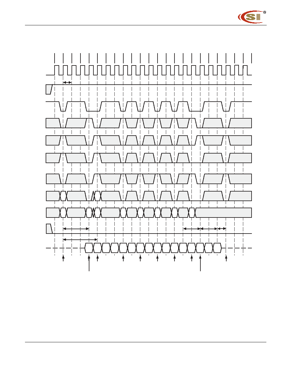
IC42S32400
IC42S32400L
Integrated Circuit Solution Inc.
47
DR038-0C 02/01/2005
Figure 15.3.Interleaved Column Write Cycle (Burst Length=4,CAS#Latency=3)
T0 T 1 T2 T3 T4 T5 T6 T7 T8 T9 T10 T 11 T12 T13 T14 T15 T16 T17 T18 T19 T20 T21 T22
t
CK3
DBw0 DBw1 DBx0 DBx1
DBy1 DAy0
RAx
RAx
DAx0 DAx1 DAx2 DAx3
DBy0
DAy1
t
RCD
CAx RBw
RBw
CBw
CBx
CBy
CAy
t
RRD
>
t
RRD(min)
t
RP
t
WR
t
WR(min)
CBz
DBz0 DBz1 DBz2 DBz3
CLK
CKE
CS#
RAS#
CAS#
WE#
BS0,1
A10
A0-A9
DQM
DQ
Hi-Z
Write
Command
Bank A
Write
Command
Bank A
Activate
Command
Bank A
Precharge
Command
Bank A
Write
Command
Bank B
Write
Command
Bank B
Write
Command
Bank B
Write
Command
Bank B
Activate
Command
Bank B
Precharge
Command
Bank B
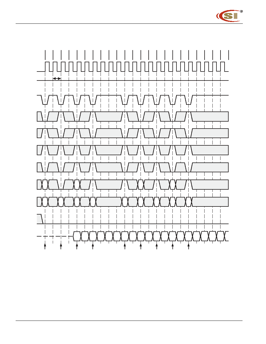
IC42S32400
IC42S32400L
48
Integrated Circuit Solution Inc.
DR038-0C 02/01/2005
Figure 16.2.Auto Precharge after Read Burst (Burst Length=4,CAS#Latency=2)
T0 T 1 T2 T3 T4 T5 T6 T7 T8 T9 T10 T 11 T12 T13 T14 T15 T16 T17 T18 T19 T20 T21 T22
t
CK2
Bx0
Bx1 Bx2
Bx3
Ay1 Ay2
RAx
RAx
RBx
Ax0
Ax1 Ax2 Ax3
Ay0
Ay3 By0
RBx
CBx
RBy
RAy
CBy
By1 By2 By3 Az0 Az1 Az2
CAx
RBy
RAz
CAz
RAz
CLK
CKE
CS#
RAS#
CAS#
WE#
BS0,1
A10
A0-A9
DQM
DQ
Hi-Z
Activate
Command
Bank A
Activate
Command
Bank A
Read
Command
Bank A
Activate
Command
Bank B
Activate
Command
Bank B
High
Read with
Auto Precharge
Command
Bank B
Read with
Auto Precharge
Command
Bank B
Read with
Auto Precharge
Command
Bank A
Read with
Auto Precharge
Command
Bank A
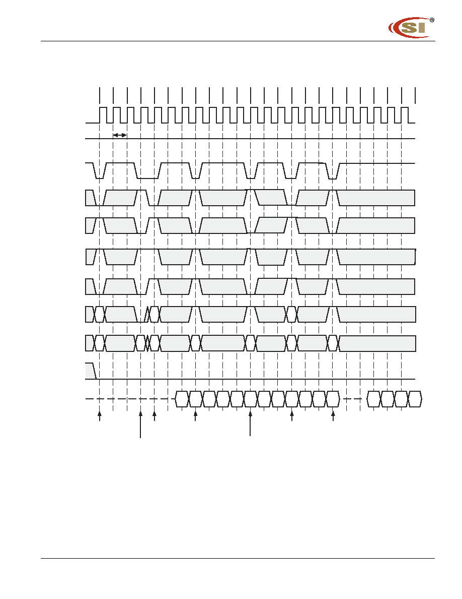
IC42S32400
IC42S32400L
Integrated Circuit Solution Inc.
49
DR038-0C 02/01/2005
Figure 16.3.Auto Precharge after Read Burst (Burst Length=4,CAS#Latency=3)
T0 T 1 T2 T3 T4 T5 T6 T7 T8 T9 T10 T 11 T12 T13 T14 T15 T16 T17 T18 T19 T20 T21 T22
t
CK3
Bx0 Bx1
Bx2
Bx3
Ay1 Ay2
RAx
RAx
RBx
Ax0
Ax1
Ax2
Ax3
Ay0
Ay3
By0
RBx
CBx
By1 By2
By3
CAx
RBy
CBy
RBy
CAy
CLK
CKE
CS#
RAS#
CAS#
WE#
BS0,1
A10
A0-A9
DQM
DQ
Hi-Z
Activate
Command
Bank A
Read
Command
Bank A
Activate
Command
Bank B
Activate
Command
Bank B
High
Read with
Auto Precharge
Command
Bank B
Read with
Auto Precharge
Command
Bank B
Read with
Auto Precharge
Command
Bank A
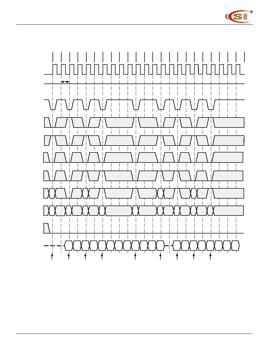
IC42S32400
IC42S32400L
50
Integrated Circuit Solution Inc.
DR038-0C 02/01/2005
Figure 17.2.Auto Precharge after Write Burst (Burst Length=4,CAS#Latency=2)
T0 T 1 T2 T3 T4 T5 T6 T7 T8 T9 T10 T 11 T12 T13 T14 T15 T16 T17 T18 T19 T20 T21 T22
t
CK2
DBx0 DBx1 DBx2 DBx3
DAy1 DAy2
RAx
RAx
RBx
DAx0 DAx1 DAx2 DAx3
DAy0
DAy3
CBx
CAy
RBy
CBy
RBy
DAz0 DAz1 DAz2 DAz3
CAx
RBx
CAz
RAz
RAz
DBy0 DBy1 DBy2 DBy3
CLK
CKE
CS#
RAS#
CAS#
WE#
BS0,1
A10
A0-A9
DQM
DQ
Hi-Z
Write
Command
Bank A
Activate
Command
Bank A
Activate
Command
Bank A
Activate
Command
Bank B
Activate
Command
Bank B
High
Write
with
Auto Precharge
Command
Bank B
Write
with
Auto Precharge
Command
Bank B
Write
with
Auto Precharge
Command
Bank A
Write
with
Auto Precharge
Command
Bank A
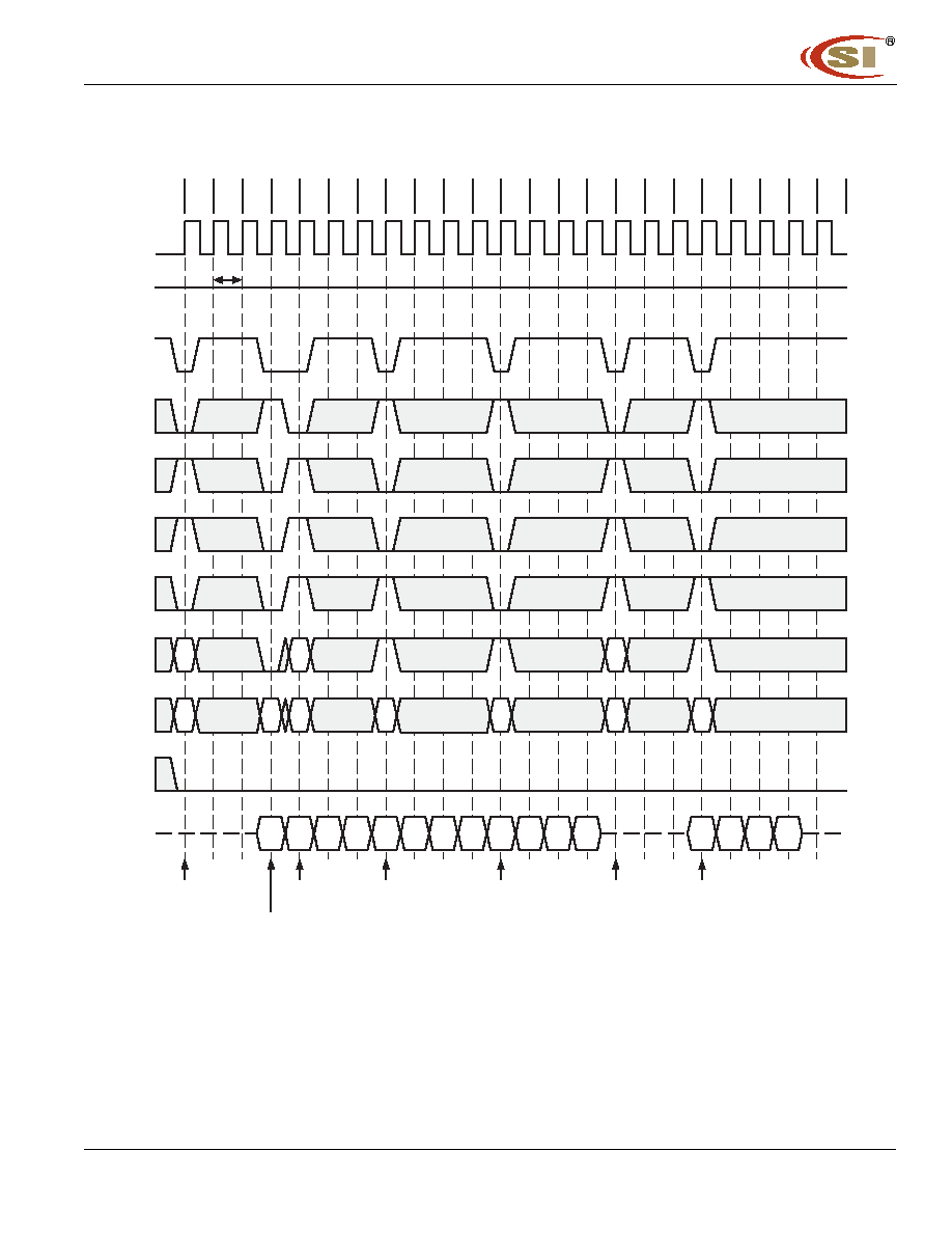
IC42S32400
IC42S32400L
Integrated Circuit Solution Inc.
51
DR038-0C 02/01/2005
Figure 17.3.Auto Precharge after Write Burst (Burst Length=4,CAS#Latency=3)
T0 T 1 T2 T3 T4 T5 T6 T7 T8 T9 T10 T 11 T12 T13 T14 T15 T16 T17 T18 T19 T20 T21 T22
t
CK3
DBx0 DBx1 DBx2 DBx3
DAy1 DAy2
RAx
RAx
RBx
DAx0 DAx1 DAx2 DAx3
DAy0
DAy3
CBx
CAy
CAx RBx
CBy
RBy
RBy
`
DBy0 DBy1 DBy2 DBy3
CLK
CKE
CS#
RAS#
CAS#
WE#
BS0,1
A9
A0-A9
DQM
DQ
Hi-Z
Write
Command
Bank A
Activate
Command
Bank A
Activate
Command
Bank B
Activate
Command
Bank B
High
Write
with
Auto Precharge
Command
Bank B
Write
with
Auto Precharge
Command
Bank B
Write
with
Auto Precharge
Command
Bank A
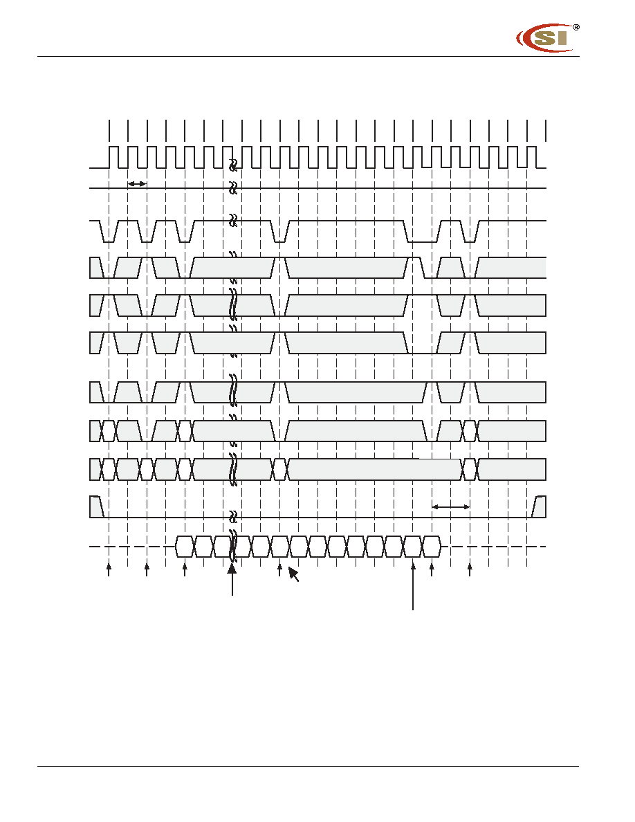
IC42S32400
IC42S32400L
52
Integrated Circuit Solution Inc.
DR038-0C 02/01/2005
Figure 18.2.Full Page Read Cycle (Burst Length=Full Page,CAS#Latency=2)
T0
T 1
T2
T3
T4
T5
T6
T7
T8
T9
T10 T 11 T12 T13 T14 T15 T16 T17 T18 T19 T20 T21 T22
Ax
Ax+1
Bx
Bx+1
Bx+3 Bx+4
RAx
RAx
Ax+1 Ax+2 Ax-2 Ax-1
B
x+2
Bx+5
CBx
RBx
CAx
RBy
RBy
Ax
Bx+6
t
CK2
t
RP
RBx
CLK
CKE
CS#
RAS#
CAS#
WE#
BS0,1
A10
A0-A9
DQM
DQ
Hi-Z
Activate
Command
Bank A
Activate
Command
Bank B
Activate
Command
Bank B
Precharge
Command
Bank B
High
Burst Stop
Command
The burst counter wraps
from the highest order
page address back to zero
during this time interval
Read
Command
Bank A
Read
Command
Bank B
Full Page burst operation does not
term in ate when the burst length is sat is fied;
the burst counter increments and continues
bursting beginning with the starting address.
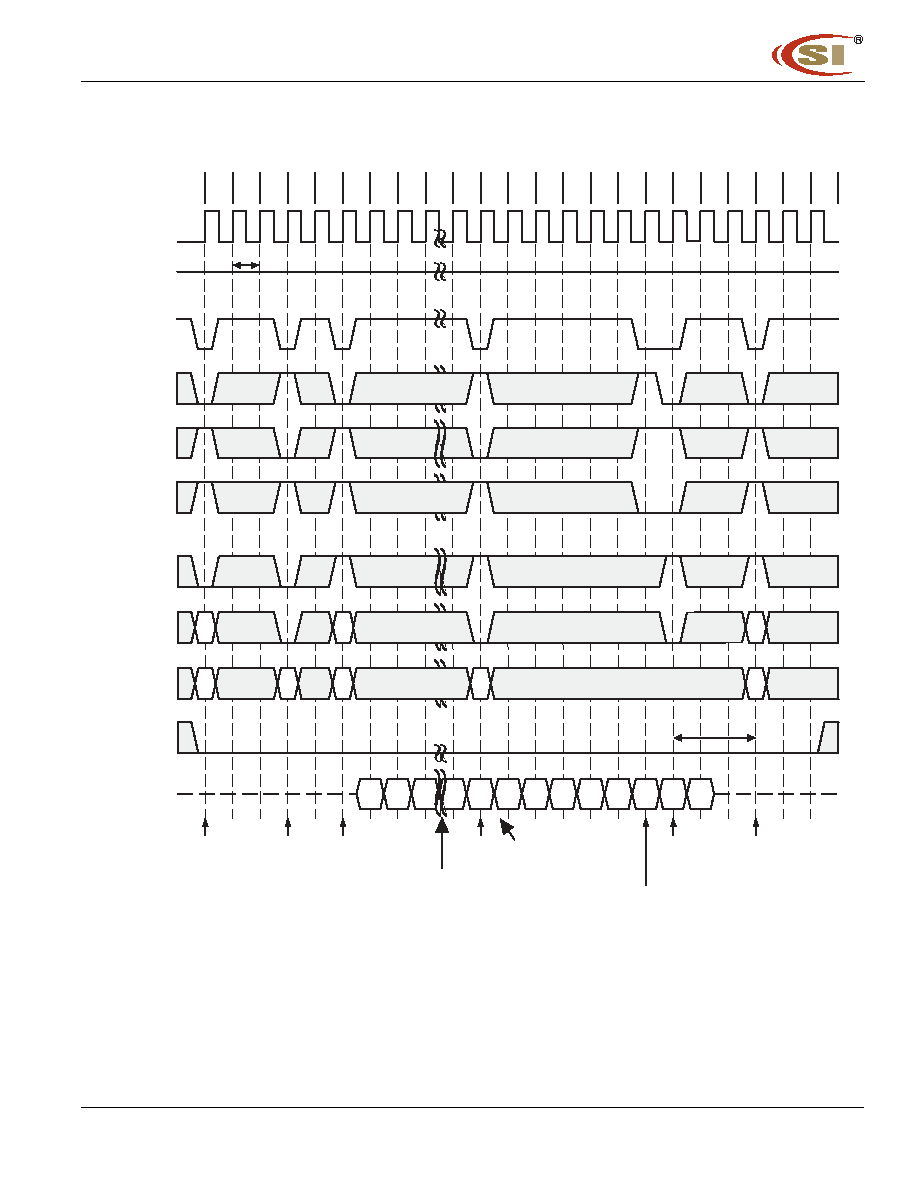
IC42S32400
IC42S32400L
Integrated Circuit Solution Inc.
53
DR038-0C 02/01/2005
Figure 18.3.Full Page Read Cycle (Burst Length=Full Page,CAS#Latency=3)
T0 T 1 T2 T3 T4 T5 T6 T7 T8 T9 T10 T 11 T12 T13 T14 T15 T16 T17 T18 T19 T20 T21 T22
Bx
Bx+1
RAx
RAx
Ax+1
Ax-2 Ax-1
CBx
RBx
CAx
RBy
RBy
Ax
t
CK3
t
RP
RBx
Ax+2
Ax Ax+1
Bx+2 Bx+3 Bx+4 Bx+5
CLK
CKE
CS#
RAS#
CAS#
WE#
BS0,1
A10
A0-A9
DQM
DQ Hi-Z
Activate
Command
Bank A
Activate
Command
Bank B
Activate
Command
Bank B
Precharge
Command
Bank B
High
Burst Stop
Command
The burst counter wraps
from the highest order
page address back to zero
during this time interval
Read
Command
Bank A
Read
Command
Bank B
Full Page burst operation does not
terminate when the burst length is
satisfied; the burst counter
increments and continues
bursting beginning with the
starting address.
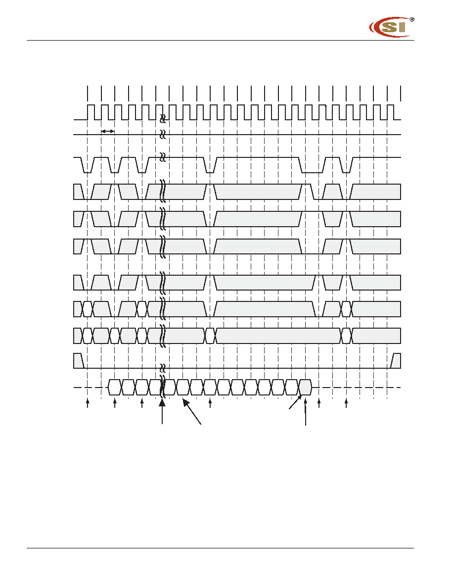
IC42S32400
IC42S32400L
54
Integrated Circuit Solution Inc.
DR038-0C 02/01/2005
Figure 19.2.Full Page Write Cycle (Burst Length=Full Page,CAS#Latency=2)
T0 T 1 T2 T3 T4 T5 T6 T7 T8 T9 T10 T 11 T12 T13 T14 T15 T16 T17 T18 T19 T20 T21 T22
RAx
RAx
CBx
RBx
CAx
RBy
RBy
t
CK2
5
RBx
DAx
DAx+1 DAx+2 DAx+3 DAx-1 DAx DAx+1 DBx
DBx+1 DBx+2 DBx+3 DBx+4 DBx+5 DBx+6
CLK
CKE
CS#
RAS#
CAS#
WE#
BS0,1
A10
A0-A9
DQM
DQ
Hi-Z
Write
Command
Bank A
Activate
Command
Bank A
Write
Command
Bank B
Activate
Command
Bank B
Activate
Command
Bank B
Precharge
Command
Bank B
High
Burst Stop
Command
Data is ignored
Full Page burst operation does
not terminate when the burst
length is satisfied; the burst counter
increments and continues bursting
beginning with the starting address.
The burst counter wraps
from the highest order
page address back to zero
during this time interval
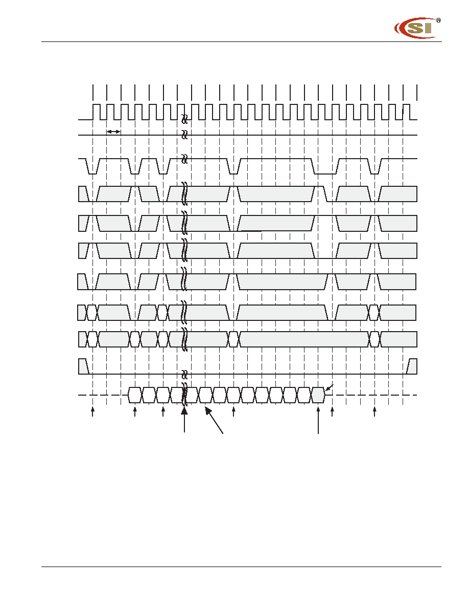
IC42S32400
IC42S32400L
Integrated Circuit Solution Inc.
55
DR038-0C 02/01/2005
Figure 19.3.Full Page Write Cycle (Burst Length=Full Page,CAS#Latency=3)
T0 T 1 T2 T3 T4 T5 T6 T7 T8 T9 T10 T 11 T12 T13 T14 T15 T16 T17 T18 T19 T20 T21 T22
RAx
RAx
CBx
RBx
CAx
RBy
RBy
t
CK3
RBx
Data is ignored
DAx
DAx+1 DAx+2 DAx+3 DAx-1 DAx DAx+1 DBx
DBx+1
DBx+3 DBx+4 DBx+5
CLK
CKE
CS#
RAS#
CAS#
WE#
BS0,1
A10
A0-A9
DQM
DQ
Hi-Z
High
Write
Command
Bank A
Activate
Command
Bank A
Write
Command
Bank B
Activate
Command
Bank B
The burst counter wraps
from the highest order
page address back to zero
during this time interval
Activate
Command
Bank B
Precharge
Command
Bank B
Burst Stop
Command
Full Page burst operation does
not terminate when the burst
length is satisfied; the burst counter
increments and continues bursting
beginning with the starting address.
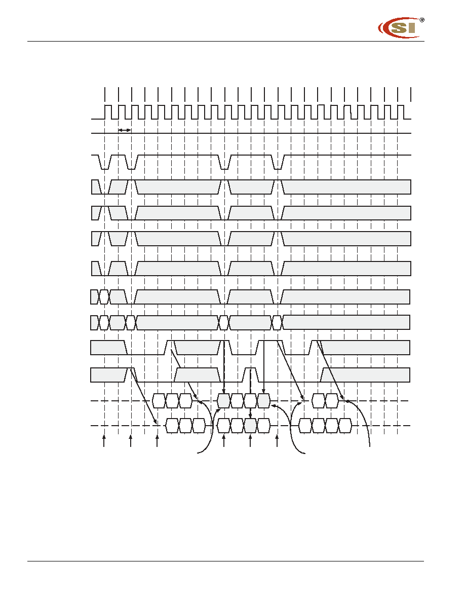
IC42S32400
IC42S32400L
56
Integrated Circuit Solution Inc.
DR038-0C 02/01/2005
Figure 20.Byte Write Operation (Burst Length=4,CAS#Latency=2)
T0 T 1 T2 T3 T4 T5 T6 T7 T8 T9 T10 T 11 T12 T13 T14 T15 T16 T17 T18 T19 T20 T21 T22
RAx
RAx
CAy
CAx
t
CK2
CAz
Ax0
Ax1
Ax2
Ax1
Ax2
Ax3
DAy1 DAy2
DAy0 DAy1
DAy3
Az1
Az2
Az1
Az2
Az3
Write
Command
Bank A
CLK
CKE
CS#
RAS#
CAS#
WE#
BS0,1
A10
A0-A9
High
Activate
Command
Bank A
Command
Bank A
DQM0
DQM1,2,3
DQ0 - DQ7
DQ8 - DQ15
Read
Command
Bank A
Read
are masked
Upper 3 Bytes
are masked
Upper 3 Bytes
Lower Byte
is masked
Lower Byte
is masked
Lower Byte
is masked
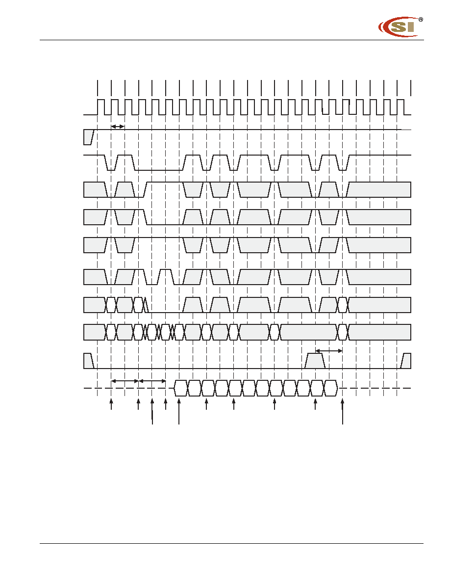
IC42S32400
IC42S32400L
Integrated Circuit Solution Inc.
57
DR038-0C 02/01/2005
Figure 22.Full Page Random Column Read (Burst Length=Full Page,CAS#Latency=2)
T0 T 1 T2 T3 T4 T5 T6 T7 T8 T9 T10 T 11 T12 T13 T14 T15 T16 T17 T18 T19 T20 T21 T22
t
CK2
Ax0
Bx0
Ay0
Ay1 By0
By1
Az0
Az1 Az2
Bz0
Bz1 Bz2
t
RP
t
RRD
t
RCD
RAx
RAx
RBx
RBx CAx CBx CAy
CBy
CAz
CBz
RBw
RBw
CLK
CKE
CS#
RAS#
CAS#
WE#
BS0,1
A10
A0-A9
DQM
DQ
Command
Bank B
Activate
Command
Bank A
Activate
Command
Bank B
Activate
Command
Bank B
Read
Command
Bank B
Read
Command
Bank B
Read
Command
Bank A
Read
Command
Bank A
Read
Command
Bank A
Read
Precharge
Command Bank B
(Precharge Temination)
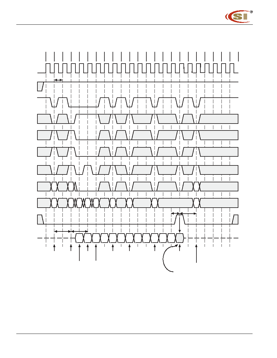
IC42S32400
IC42S32400L
58
Integrated Circuit Solution Inc.
DR038-0C 02/01/2005
Figure 23.Full Page Random Column Write (Burst Length=Full Page,CAS#Latency=2)
T0 T 1 T2 T3 T4 T5 T6 T7 T8 T9 T10 T 11 T12 T13 T14 T15 T16 T17 T18 T19 T20 T21 T22
t
CK2
DAx0 DBx0 DAy0 DAy1 DBy0 DBy1 DAz0 DAz1 DAz2 DBz0
t
RP
t
RRD
t
RCD
RAx
RAx
RBx
RBx CAx
CBx CAy
CBy
CAz
CBz
RBw
RBw
t
WR
DBz1 DBz2
CLK
CKE
CS#
RAS#
CAS#
WE#
BS0,1
A10
A0-A9
DQM
DQ
Write
Command
Bank A
Write
Command
Bank A
Write
Command
Bank A
Activate
Command
Bank A
Write
Command
Bank B
Write
Command
Bank B
Write
Command
Bank B
Activate
Command
Bank B
Activate
Command
Bank B
Precharge
Command Bank B
(Precharge Temination)
Write Data
is masked
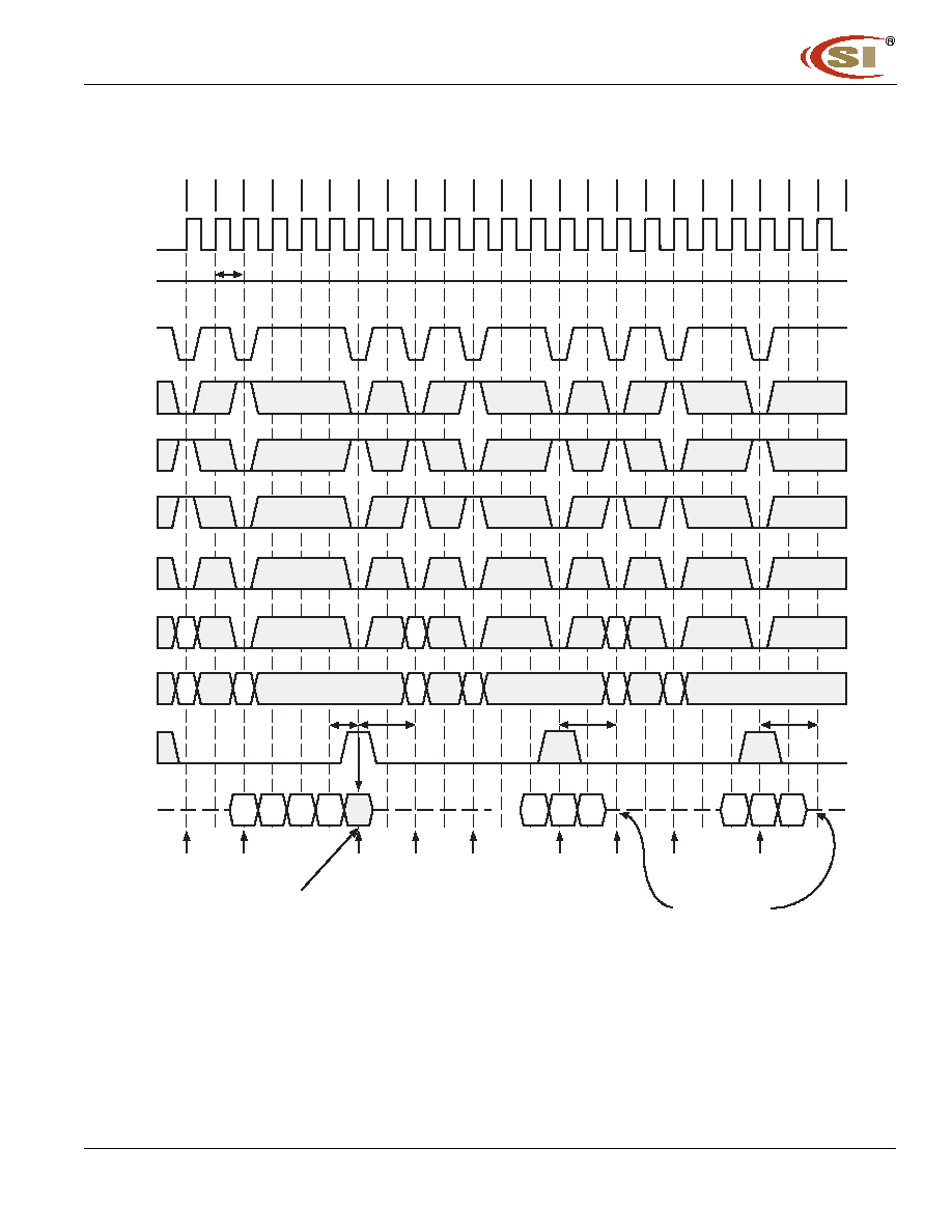
IC42S32400
IC42S32400L
Integrated Circuit Solution Inc.
59
DR038-0C 02/01/2005
Figure 24.2.Precharge Termination of a Burst
(Burst Length=8 or Full Page,CAS#Latency=2)
T0 T 1 T2 T3 T4 T5 T6 T7 T8 T9 T10 T 11 T12 T13 T14 T15 T16 T17 T18 T19 T20 T21 T22
t
CK2
DAx0 DAx1 DAx2 DAx3
Ay2
Ay0
Ay1
RAx
RAx
RAy
CAx
RAy
CAy
Az0
Az1
Az2
t
WR
t
RP
t
RP
RAz
CAz
t
RP
RAz
CLK
CKE
CS#
RAS#
CAS#
WE#
BS0,1
A10
A0-A9
DQM
DQ
High
Write
Command
Bank A
Activate
Command
Bank A
Activate
Command
Bank A
Activate
Command
Bank A
Command
Bank A
Precharge
Command
Bank A
Precharge
Command
Bank A
Precharge
Command
Bank A
Read
Command
Bank A
Read
Precharge Termination
of a Write Burst.
Precharge Termination
of a Read Burst.
Write data is masked.
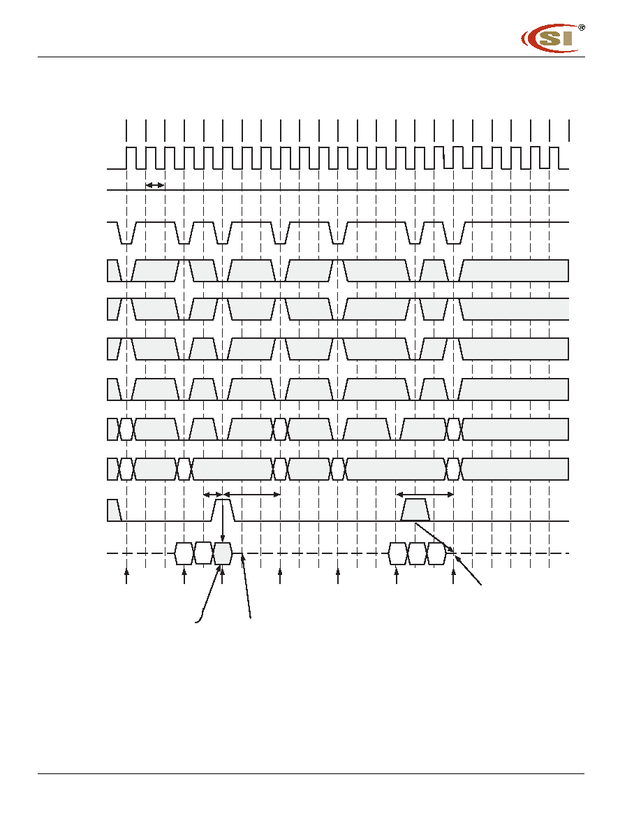
IC42S32400
IC42S32400L
60
Integrated Circuit Solution Inc.
DR038-0C 02/01/2005
Figure 24.3.Precharge Termination of a Burst
(Burst Length=4,8 or Full Page,CAS#Latency=3)
T0 T 1 T2 T3 T4 T5 T6 T7 T8 T9 T10 T 11 T12 T13 T14 T15 T16 T17 T18 T19 T20 T21 T22
t
CK3
DAx0
Ay0
Ay1
Ay2
RAx
RAx
RAy
CAx
RAy
CAy
t
WR
t
RP
t
RP
RAz
RAz
DAx1
CLK
CKE
CS#
RAS#
CAS#
WE#
BS0,1
A10
A0-A9
DQM
DQ
High
Write
Command
Bank A
Command
Bank A
Activate
Command
Bank A
Activate
Command
Bank A
Activate
Command
Bank A
Precharge
Command
Bank A
Precharge
Command
Bank A
Write Data
is masked
Precharge Termination
of a Write Burst
Precharge Termination
of a Read Burst
Read

IC42S32400
IC42S32400L
Integrated Circuit Solution Inc.
61
DR038-0C 02/01/2005
ORDERING INFORMATION
Commercial Range: 0
C to 70
C
Frequency
Speed (ns)
Order Part No.
Package
166MHz
6
IC42S32400/L-6T
400mil TSOP-2
166MHz
6
IC42S32400/L-6B
11*13mm BGA
143MHz
7
IC42S32400/L-7T
400mil TSOP-2
143MHz
7
IC42S32400/L-7B
11*13mm BGA
125MHz
8
IC42S32400/L-8T
400mil TSOP-2
125MHz
8
IC42S32400/L-8B
11*13mm BGA
ORDERING INFORMATION
Industrial Temperature Range: -40
C to 85
C
Frequency
Speed (ns)
Order Part No.
Package
166MHz
6
IC42S32400/L-6TI
400mil TSOP-2
166MHz
6
IC42S32400/L-6BI
11*13mm BGA
143MHz
7
IC42S32400/L-7TI
400mil TSOP-2
143MHz
7
IC42S32400/L-7BI
11*13mm BGA
125MHz
8
IC42S32400/L-8TI
400mil TSOP-2
125MHz
8
IC42S32400/L-8BI
11*13mm BGA

IC42S32400
IC42S32400L
62
Integrated Circuit Solution Inc.
DR038-0C 02/01/2005
Integrated Circuit Solution Inc.
HEADQUARTER:
NO.2, TECHNOLOGY RD. V, SCIENCE-BASED INDUSTRIAL PARK,
HSIN-CHU, TAIWAN, R.O.C.
TEL: 886-3-5780333
Fax: 886-3-5783000
BRANCH OFFICE:
7F, NO. 106, SEC. 1, HSIN-TAI 5
TH
ROAD,
HSICHIH TAIPEI COUNTY, TAIWAN, R.O.C.
TEL: 886-2-26962140
FAX: 886-2-26962252
http://www.icsi.com.tw
ORDERING INFORMATION (Pb-free Package)
Commercial Range: 0
C to 70
C
Frequency
Speed (ns)
Order Part No.
Package
166MHz
6
IC42S32400/L-6TG 400mil TSOP-2
166MHz
6
IC42S32400/L-6BG
11*13mm BGA
143MHz
7
IC42S32400/L-7TG 400mil TSOP-2
143MHz
7
IC42S32400/L-7BG
11*13mm BGA
125MHz
8
IC42S32400/L-8TG 400mil TSOP-2
125MHz
8
IC42S32400/L-8BG
11*13mm BGA
ORDERING INFORMATION (Pb-free Package)
Industrial Temperature Range: -40
C to 85
C
Frequency
Speed (ns)
Order Part No.
Package
166MHz
6
IC42S32400/L-6TIG 400mil TSOP-2
166MHz
6
IC42S32400/L-6BIG 11*13mm BGA
143MHz
7
IC42S32400/L-7TIG 400mil TSOP-2
143MHz
7
IC42S32400/L-7BIG 11*13mm BGA
125MHz
8
IC42S32400/L-8TIG 400mil TSOP-2
125MHz
8
IC42S32400/L-8BIG 11*13mm BGA