
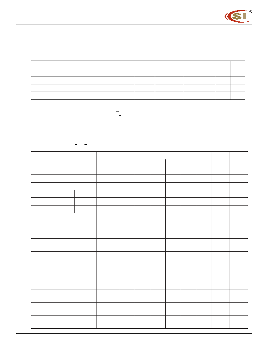
IC43R16160
Integrated Circuit Solution Inc.
1
DDR001-0B 11/10/2004
Document Title
4M x 16 Bit x 4 Banks (256-MBIT) DDR SDRAM
Revision History
Revision No
History
Draft Date
Remark
0A
Initial Draft
January 13,2004
0B
Mass production
November 10,2004
The attached datasheets are provided by ICSI. Integrated Circuit Solution Inc reserve the right to change the specifications and
products. ICSI will answer to your questions about device. If you have any questions, please contact the ICSI offices.
Features
High speed data transfer rates with system frequency
up to 200 MHz
Data Mask for Write Control
Four Banks controlled by BA0 & BA1
Programmable CAS Latency: 2, 2.5, 3
Programmable Wrap Sequence: Sequential
or Interleave
Programmable Burst Length:
2, 4, 8 for Sequential Type
2, 4, 8 for Interleave Type
Automatic and Controlled Precharge Command
Power Down Mode
Auto Refresh and Self Refresh
Refresh Interval: 8192 cycles/64 ms
Available in 66-pin 400 mil TSOP
SSTL-2 Compatible I/Os
Double Data Rate (DDR)
Bidirectional Data Strobe (DQS) for input and output
data, active on both edges
On-Chip DLL aligns DQ and DQs transitions with CK
transitions
Differential clock inputs CK and CK
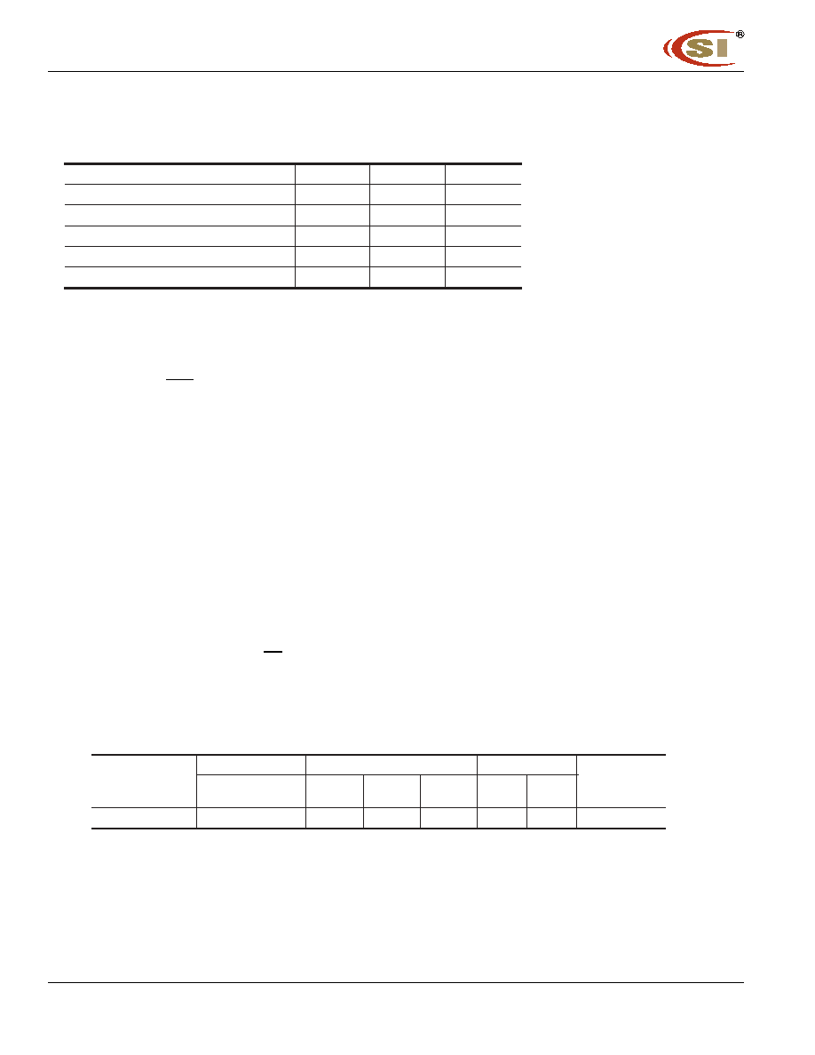
5
6
7
DDR400
DDR333
DDR266
Clock Cycle Time (t
CK2
)
7.5ns
7.5ns
7.5ns
Clock Cycle Time (t
CK2.5
)
6ns
6ns
7ns
Clock Cycle Time (t
CK3
)
5ns
-
-
System Frequency (f
CK max
)
200MHz
166MHz
143MHz
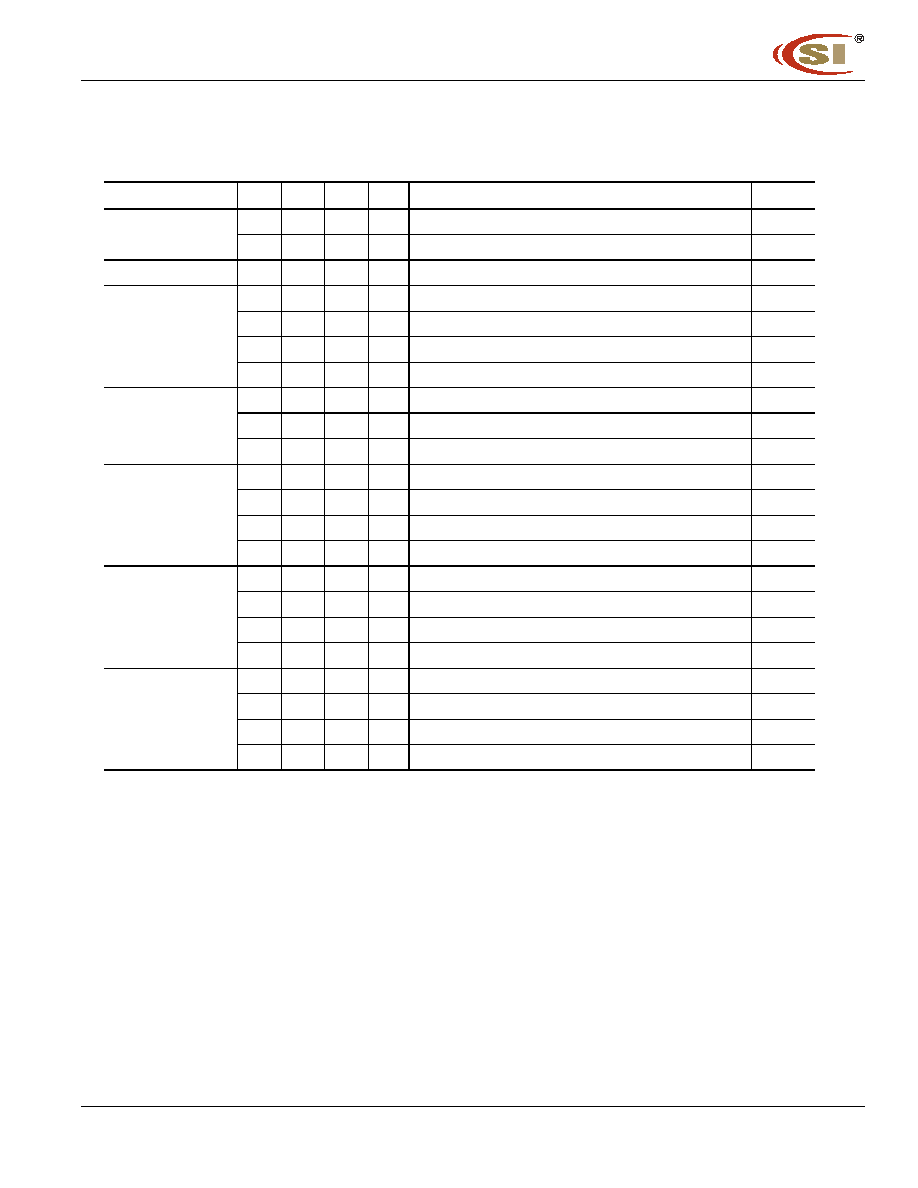
Package Outline
JESEC 66TSOP II
-5
-6
-7
Std.
L
0�C to 70�C
�
�
�
�
�
�
Blank
Operation
Temperature
Range
CK Cycle Time (ns)
Power
Temperature
Mark
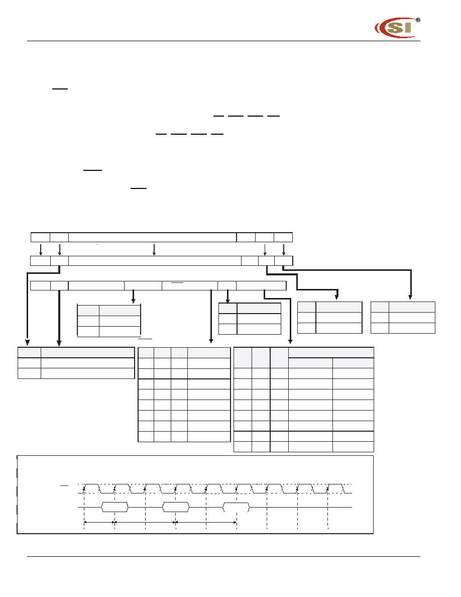
The ICSI IC43R16160 is a four bank DDR DRAM
organized as 4 banks x 4Mbit x 16. The IC43R16160
achieves high speed data transfer rates by employing a
chip architecture that prefetches multiple bits and then
synchronizes the output data to a system clock.
All of the control, address, circuits are synchronized with
the positive edge of an externally supplied clock. I/O
transactions are ocurring on both edges of DQS. Operating
the four memory banks in an interleaved fashion allows
random access operation to occur at a higher rate than is
possible with standard DRAMs. A sequential and gapless
data rate is possible depending on burst length,
CAS
latency and speed grade of the device.
Device Usage Chart
IC4
3R16160
2 Integrated Circuit Solution Inc.
DDR001
-
0B
11
/
10
/
2004
4M Words x 16 Bits x 4 Banks (256-MBIT)
DDR SYNCHRONOUS DYNAMIC RAM
66 Pin Plastic TSOP-II
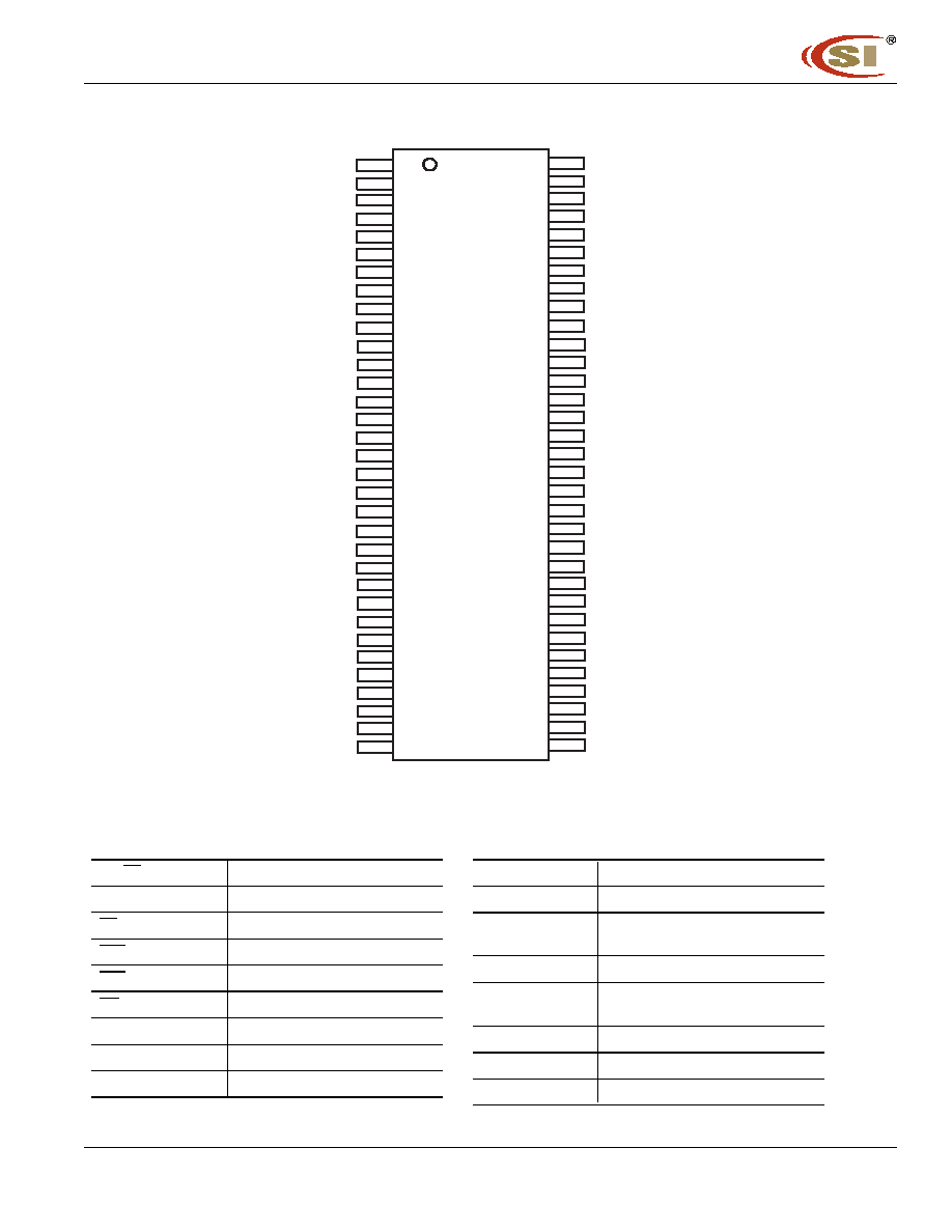
PIN CONFIGURATION
Top View
Pin Names
CK, CK
Differential Clock Input
CKE
Clock Enable
CS
Chip Select
RAS
Row Address Strobe
CAS
Column Address Strobe
WE
Write Enable
DQS (UDQS, LDQS)
Data Strobe (Bidirectional)
A
0
�A
12
Address Inputs
BA0, BA1
Bank Select
DQ's
Data Input/Output
DM (UDM, LDM)
Data Mask
V
DD
Power
(+2.5V and +2.6V for DDR400)
V
SS
Ground
V
DDQ
Power for I/O's
(+2.5V and +2.6V for DDR400)
V
SSQ
Ground for I/O's
NC
Not connected
VREF
Reference Voltage for Inputs
VDD
DQ0
VDDQ
DQ1
DQ2
VSSQ
DQ3
DQ4
VDDQ
DQ5
DQ6
VSSQ
DQ7
NC
VDDQ
LDQS
NC
VDD
NC
LDM
WE
CAS
RAS
CS
N C
B A 0
B A 1
AP/A10
A0
A1
A2
A3
VDD
VSS
DQ15
VSSQ
DQ14
DQ13
VDDQ
DQ12
DQ11
VSSQ
DQ10
DQ9
VDDQ
DQ8
NC
VSSQ
UDQS
NC
VREF
VSS
UDM
CK
C K
C K E
N C
A 1 2
A 11
A 9
A8
A7
A6
A5
A4
VSS
1
2
3
4
5
6
7
8
9
1 0
11
1 2
1 3
1 4
1 5
1 6
1 7
1 8
1 9
2 0
2 1
2 2
2 3
2 4
2 5
2 6
2 7
2 8
2 9
3 0
3 1
3 2
3 3
6 6
6 5
6 4
6 3
6 2
6 1
6 0
5 9
5 8
5 7
5 6
5 5
5 4
5 3
5 2
5 1
5 0
4 9
4 8
4 7
4 6
4 5
4 4
4 3
4 2
4 1
4 0
3 9
3 8
3 7
3 6
3 5
3 4
IC4
3R16160
Integrated Circuit Solution Inc.
3
DDR001-0B
11
/
10
/
2004
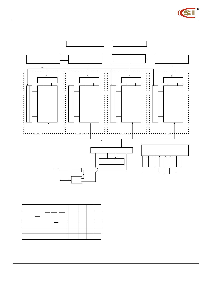
Block Diagram
Row decoder
Memory array
Bank 0
8192 x 256
x32 bit
C
o
l
umn
dec
oder
S
ens
e
ampl
i
f
i
er
&
I(
O
)
bus
Row decoder
Memory array
Bank 1
C
ol
umn d
ec
o
der
S
e
ns
e
ampl
i
f
i
er
&
I(
O
)
bus
Row decoder
Memory array
Bank 2
C
o
l
u
m
n
de
c
o
de
r
S
ens
e
ampl
i
f
i
er
&
I
(
O
)
bus
Row decoder
Memory array
Bank 3
Col
u
m
n
de
c
o
d
e
r
S
ens
e ampl
i
f
i
er
&
I
(
O
)
bus
Input buffer
Output buffer
DQ
0
-DQ
15
Column address
counter
Column address
buffer
Row address
buffer
Refresh Counter
A0 - A12, BA0, BA1
A0 - A8, AP, BA0, BA1
Control logic & timing generator
CK
CK
E
CS
RA
S
CA
S
WE
DM
Row Addresses
Column Addresses
DLL
Strobe
Gen.
Data Strobe
CK, CK
CK
DQS
8192 x 256
x 32 bit
8192 x 256
x 32 bit
8192 x 256
x 32 bit
16M x 16
Capacitance*
T
A
= 0 to 70
�
C, V
CC
= 2.5V
�
0.2V, V
CC
= 2.6V
�
0.1V
for DDR400, f = 1 Mhz
*Note: Capacitance is sampled and not 100% tested.
Absolute Maximum Ratings*
Operating temperature range ..................0 to 70 �C
Storage temperature range ................-55 to 150 �C
V
DD
Supply Voltage Relative to V
SS
.....-1V to +3.6V
V
DDQ
Supply Voltage Relative to V
SS
......................................................-1V to +3.6V
VREF and Inputs Voltage Relative to V
SS
......................................................-1V to +3.6V
I/O Pins Voltage Relative to V
SS
.......................................... -0.5V to V
DDQ
+0.5V
Power dissipation .......................................... 1.6 W
Data out current (short circuit) ...................... 50 mA
*Note: Stresses above those listed under "Absolute Maximum
Ratings" may cause permanent damage of the device.
Exposure to absolute maximum rating conditions for
extended periods may affect device reliability.
Input Capacitance
Symbol
Min Max Unit
BA0, BA1, CKE, CS, RAS, (CAS,
A0-A11, WE)
C
INI
2
3.0
pF
Input Capacitance (CK, CK)
C
IN2
2
3.0
pF
Data & DQS I/O Capacitance
C
OUT
4
5
pF
Input Capacitance (DM)
C
IN3
4
5.0
pF
IC4
3R16160
4
Integrated Circuit Solution Inc.
DDR001
-
0B
11
/
10
/
2004
Signal Pin Description
IC4
3R16160
Pin
Type Signal
Polarity
Function
CK
CK
Input
Pulse
Positive
Edge
The system clock input. All inputs except DQs and DMs are sampled on the rising
edge of CK.
CKE
Input
Level Active High
Activates the CK signal when high and deactivates the CK signal when low, thereby
initiates either the Power Down mode, or the Self Refresh mode.
CS
Input
Pulse Active Low
CS enables the command decoder when low and disables the command decoder
when high. When the command decoder is disabled, new commands are ignored
but previous operations continue.
RAS,CAS
WE
Input
Pulse Active Low
When sampled at the positive rising edge of the clock, CAS, RAS, and WE define
the command to be executed by the SDRAM.
DQS
Input/
Output
Pulse Active High
Active on both edges for data input and output.
Center aligned to input data
Edge aligned to output data
A0 - A12
Input
Level
_
During a Bank Activate command cycle, A0-A12 defines the row address (RA0-
RA12) when sampled at the rising clock edge.
During a Read or Write command cycle, A0-A8 defines the column address (CA0-
CA8) when sampled at the rising clock edge.
In addition to the column address, A10(=AP) is used to invoke autoprecharge
operation at the end of the burst read or write cycle. If A10 is high, autoprecharge is
selected and BA0, BA1 defines the bank to be precharged. If A10 is low,
autoprecharge is disabled. During a Precharge command cycle, A10(=AP) is used in
conjunction with BA0 and BA1 to control which bank(s) to precharge. If A10 is high,
all four banks will be precharged simultaneously regardless of state of BA0 and BA1.
BA0,
BA1
Input
Level
_
Selects which bank is to be active.
DQx
Input/
Output
Level
_
Data Input/Output pins operate in the same manner as on conventional DRAMs.
DM,
LDM,
UDM
Input
Pulse Active High
In Write mode, DM has a latency of zero and operates as a word mask by allowing
input data to be written if it is low but blocks the write operation if is high for LDM
corresponds to data on DQ0-DQ7, UDM corresponds to data on DQ8-DQ15.
VDD,VSS Supply
Power and ground for the input buffers and the core logic.
VDDQ
VSSQ
Supply
_
_
Isolated power supply and ground for the output buffers to provide improved noise
immunity.
VREF
Input
Level
_
SSTL Reference Voltage for Inputs
Integrated Circuit Solution Inc.
5
DDR001-0B
11
/
10
/
2004
Mode Register Set (MRS)
The mode register stores the data for controlling the various operating modes of DDR SDRAM. It programs
CAS latency, addressing mode, burst length, test mode, DLL reset and various vendor specific options to
make DDR SDRAM useful for a variety of different applications. The default value of the mode register is not
defined, therefore the mode register must be written after EMRS setting for proper DDR SDRAM operation.
The mode register is written by asserting low on CS, RAS, CAS, WE and BA
0
(The DDR SDRAM should be
in all bank precharge with CKE already high prior to writing into the mode register). The state of address pins
A
0
~ A
12
in the same cycle as CS, RAS, CAS, WE and BA0 low is written in the mode register. Two clock
cycles are required to meet t
MRD
spec. The mode register contents can be changed using the same com-
mand and clock cycle requirements during operation as long as all banks are in the idle state. The mode reg-
ister is divided into various fields depending on functionality. The burst length uses A
0
~ A
2
, addressing mode
uses A
3
, CAS latency (read latency from column address) uses A
4
~ A
6
. A
8
is used for DLL reset. A7 must
be set to low for normal MRS operation. Refer to the table for specific codes for various burst length,
addressing modes and CAS latencies.
1. MRS can be issued only at all banks precharge state.
2.
Minimum tRP is required to issue MRS command.
Address Bus
CAS Latency
A
6
A
5
A
4
Latency
0
0
0
Reserve
0
0
1
Reserve
0
1
0
2
0
1
1
3
1
0
0
Reserve
Reserve
1
0
1
1
1
0
2.5
1
1
1
Reserve
Burst Length
A
2
A
1
A
0
Latency
Sequential
Interleave
0
0
0
Reserve
Reserve
0
0
1
2
2
0
1
0
4
4
0
1
1
8
8
1
0
0
Reserve
Reserve
1
0
1
Reserve
Reserve
1
1
0
Reserve
Reserve
1
1
1
Reserve
Reserve
A
3
Burst Type
0
Sequential
1
Interleave
* RFU(Reserved for future use)
should stay "0" during MRS
cycle.
A
8
DLL Reset
0
No
1
Yes
Mode Register Set
0
RFU : Must be set "0"
Extended Mode Register
Mode Register
DLL
I/O
A
0
DLL Enable
0
Enable
1
Disable
A
1
I/O Strength
0
Full
1
Half
BA
0
A
n
~ A
0
0
(Existing)MRS Cycle
1
Extended Funtions(EMRS)
Command
2
0
1
5
3
4
8
6
7
CK, CK
t
CK
t
MRD
Precharge
All Banks
Mode
Register Set
t
RP
*2
*1
Any
Command
BA
1
BA
0
A
3
A
2
A
1
A
0
0
CAS Latency
BT
Burst Length
RFU
DLL
MRS
MRS
A
12
to
IC4
3R16160
6 Integrated Circuit Solution Inc.
DDR001
-
0B
11
/
10
/
2004
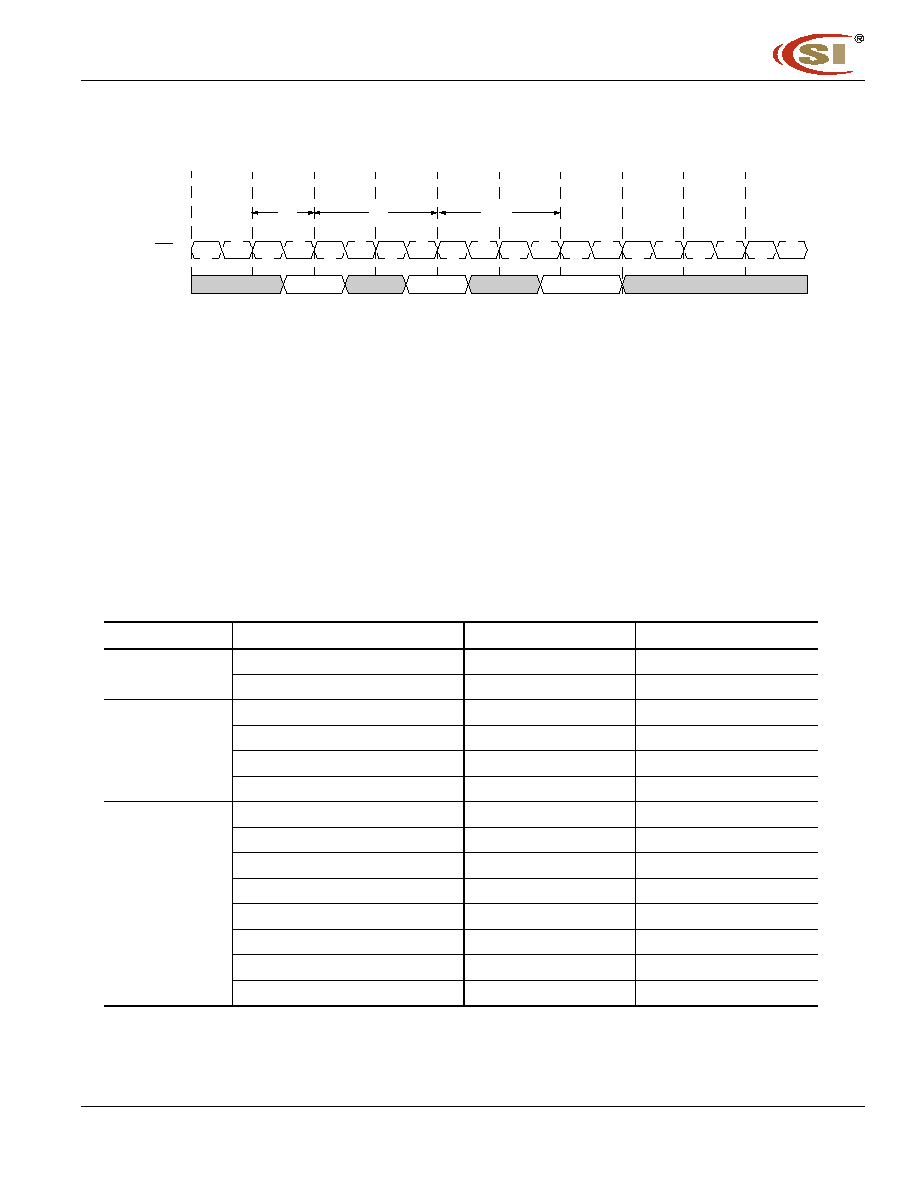
Mode Register Set Timing
Burst Mode Operation
Burst Mode Operation is used to provide a constant flow of data to memory locations (Write cycle), or from
memory locations (Read cycle). Two parameters define how the burst mode will operate: burst sequence and
burst length. These parameters are programmable and are determined by address bits A
0
--A
3
during the
Mode Register Set command. Burst type defines the sequence in which the burst data will be delivered or
stored to the SDRAM. Two types of burst sequence are supported: sequential and interleave. The burst
length controls the number of bits that will be output after a Read command, or the number of bits to be input
after a Write command. The burst length can be programmed to values of 2, 4, or 8. See the Burst Length
and Sequence table below for programming information.
Burst Length and Sequence
Burst Length
Starting Length (A
2
, A
1
, A
0
)
Sequential Mode
Interleave Mode
2
xx0
0, 1
0, 1
xx1
1, 0
1, 0
4
x00
0, 1, 2, 3
0, 1, 2, 3
x01
1, 2, 3, 0
1, 0, 3, 2
x10
2, 3, 0, 1
2, 3, 0, 1
x11
3, 0, 1, 2
3, 2, 1, 0
8
000
0,1, 2, 3, 4, 5, 6, 7
0,1, 2, 3, 4, 5, 6, 7
001
1, 2, 3, 4, 5, 6, 7, 0
1, 0, 3, 2, 5, 4, 7, 6
010
2, 3, 4, 5, 6, 7, 0, 1
2, 3, 0, 1, 6, 7, 4, 5
011
3, 4, 5, 6, 7, 0, 1, 2
3, 2, 1, 0, 7, 6, 5, 4
100
4, 5, 6, 7, 0, 1, 2, 3
4, 5, 6, 7, 0, 1, 2, 3
101
5, 6, 7, 0, 1, 2, 3, 4
5, 4, 7, 6, 1, 0, 3, 2
110
6, 7, 0, 1, 2, 3, 4, 5
6, 7, 4, 5, 2, 3, 0, 1
111
7, 0, 1, 2, 3, 4, 5, 6
7, 6, 5, 4, 3, 2, 1, 0
T5
T0
T1
T2
T3
T4
T6
T7
T8
t
RP
t
MRD
t
CK
Pre- All
MRS/EMRS
ANY
Mode Register set (MRS) or Extended Mode Register Set (EMRS) can be issued only when all banks are in the idle state.
CK, CK
Command
If a MRS command is issued to reset the DLL, then an additional 200 clocks must occur prior to issuing any new command
T9
to allow time for the DLL to lock onto the clock.
IC4
3R16160
Integrated Circuit Solution Inc.
7
DDR001-0B
11
/
10
/
2004
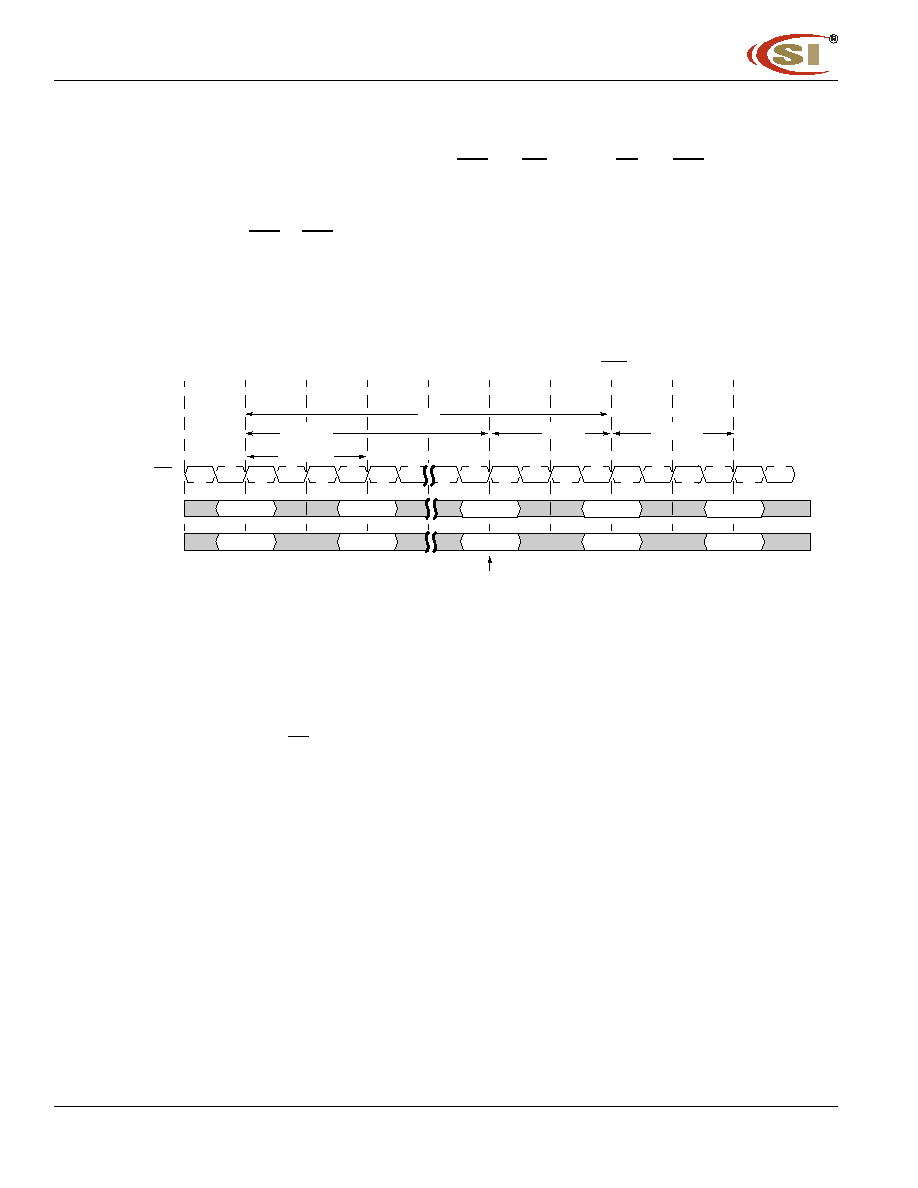
Bank Activate Command
The Bank Activate command is issued by holding CAS and WE high with CS and RAS low at the rising
edge of the clock. The DDR SDRAM has four independent banks, so two Bank Select addresses (BA
0
and
BA
1
) are supported. The Bank Activate command must be applied before any Read or Write operation can
be executed. The delay from the Bank Activate command to the first Read or Write command must meet or
exceed the minimum RAS to CAS delay time (t
RCD
min). Once a bank has been activated, it must be pre-
charged before another Bank Activate command can be applied to the same bank. The minimum time interval
between interleaved Bank Activate commands (Bank A to Bank B and vice versa) is the Bank to Bank delay
time (t
RRD
min).
Bank Activation Timing
Read Operation
With the DLL enabled, all devices operating at the same frequency within a system are ensured to have
the same timing relationship between DQ and DQS relative to the CK input regardless of device density, pro-
cess variation, or technology generation.
The data strobe signal (DQS) is driven off chip simultaneously with the output data (DQ) during each read
cycle. The same internal clock phase is used to drive both the output data and data strobe signal off chip to
minimize skew between data strobe and output data. This internal clock phase is nominally aligned to the
input differential clock (CK, CK) by the on-chip DLL. Therefore, when the DLL is enabled and the clock fre-
quency is within the specified range for proper DLL operation, the data strobe (DQS), output data (DQ), and
the system clock (CK) are all nominally aligned.
Since the data strobe and output data are tightly coupled in the system, the data strobe signal may be de-
layed and used to latch the output data into the receiving device. The tolerance for skew between DQS and
DQ (t
DQSQ
) is tighter than that possible for CK to DQ (t
AC
) or DQS to CK (t
DQSCK
).
T0
T1
T2
T3
Tn
Tn+1
Tn+2
Tn+3
Tn+4
Tn+5
(CAS Latency = 2; Burst Length = Any)
t
RRD
(min)
t
RP
(min)
t
RC
t
RCD
(min)
Begin Precharge Bank A
CK, CK
BA/Address
Command
Bank/Col
Read/A
Bank/Row
Activate/A
Activate/B
Pre/A
Bank/Row
Activate/A
Bank
Bank/Row
t
RAS
(min)
IC4
3R16160
8 Integrated Circuit Solution Inc.
DDR001
-
0B
11
/
10
/
2004
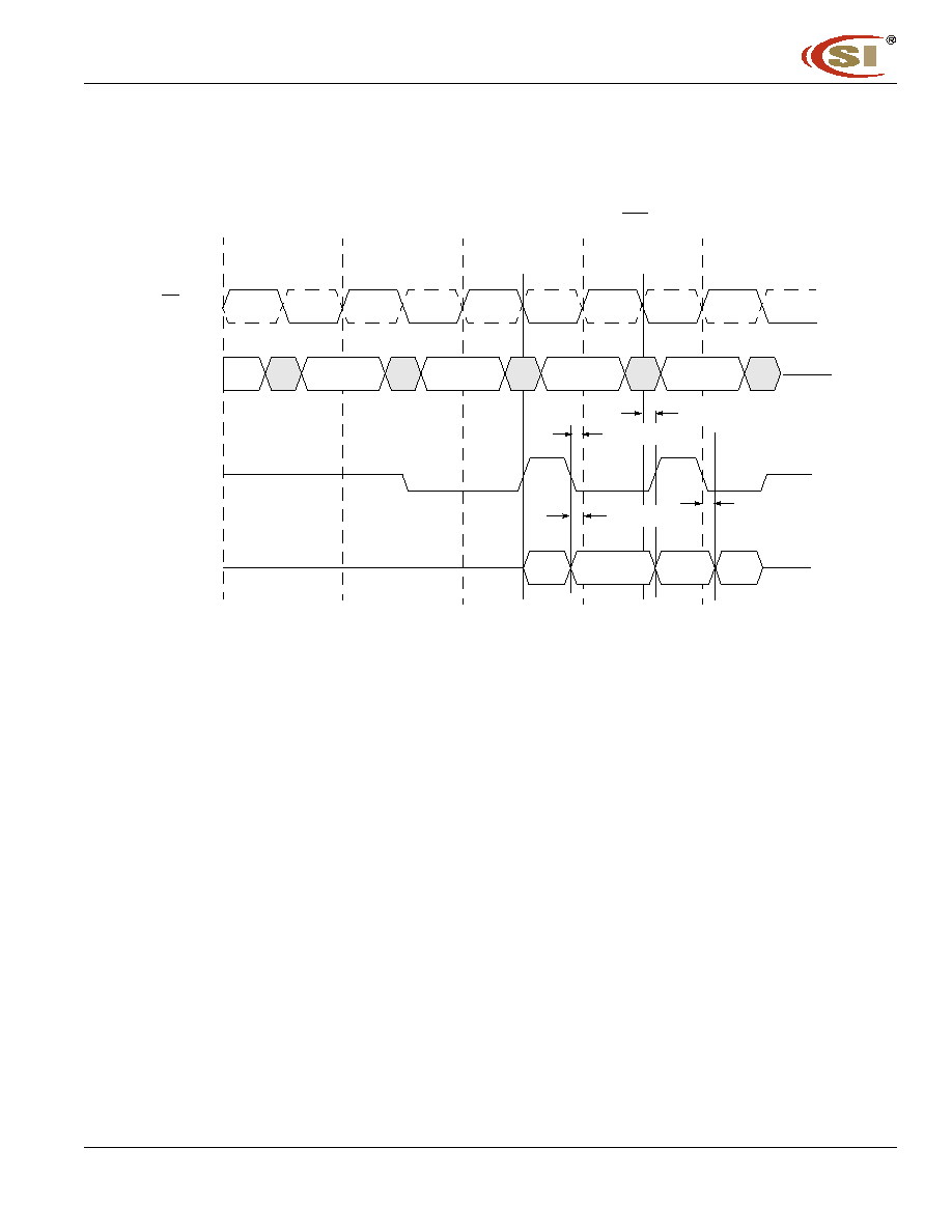
Output Data (DQ) and Data Strobe (DQS) Timing Relative to the Clock (CK)
During Read Cycles
The minimum time during which the output data (DQ) is valid is critical for the receiving device (i.e., a mem-
ory controller device). This also applies to the data strobe during the read cycle since it is tightly coupled to
the output data. The minimum data output valid time (t
DV
) and minimum data strobe valid time (t
DQSV
) are de-
rived from the minimum clock high/low time minus a margin for variation in data access and hold time due to
DLL jitter and power supply noise.
(CAS Latency = 2.5; Burst Length = 4)
T0
T1
T2
T3
T4
NOP
NOP
NOP
D
0
CK, CK
Command
DQS
DQ
D
2
t
DQSCK
(max)
t
DQSCK
(min)
D
1
t
AC
(min)
t
AC
(max)
D
3
READ
NOP
IC4
3R16160
Integrated Circuit Solution Inc.
9
DDR001-0B
11
/
10
/
2004
Output Data and Data Strobe Valid Window for DDR Read Cycles
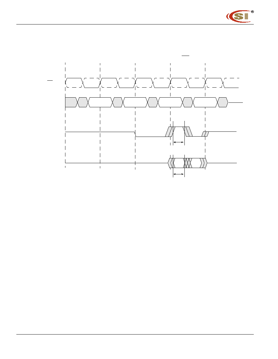
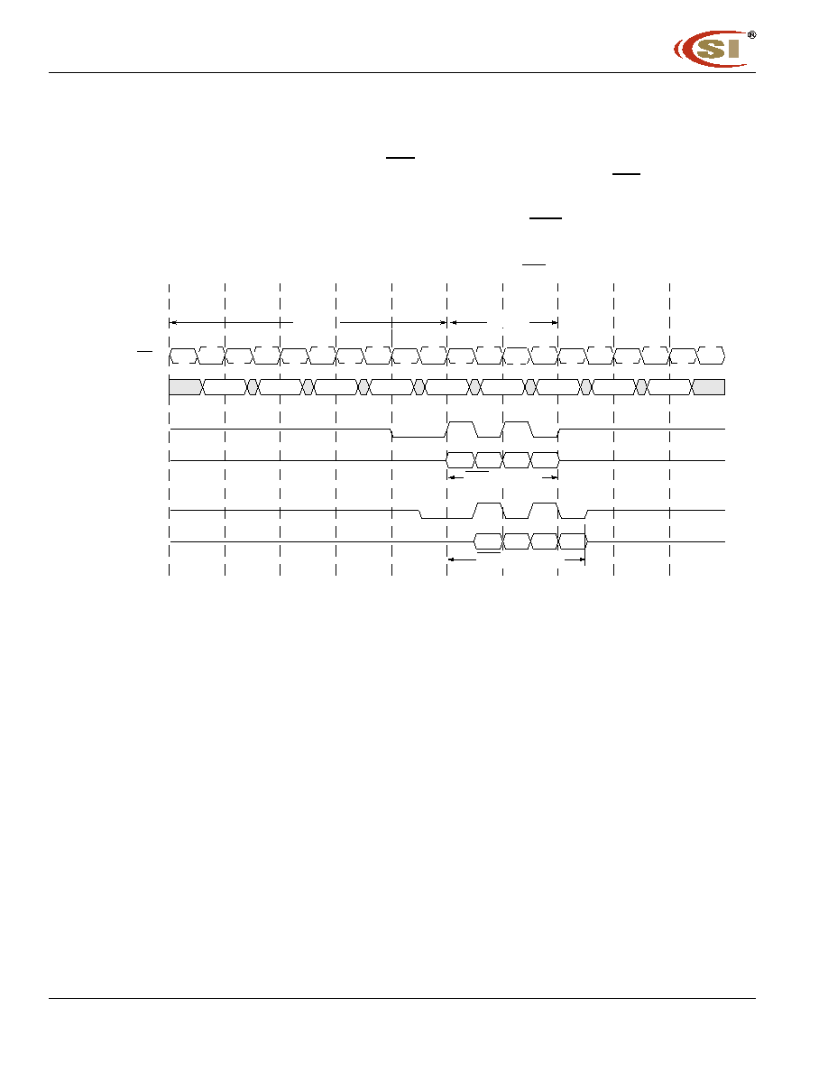
Read Preamble and Postamble Operation
Prior to a burst of read data and given that the controller is not currently in burst read mode, the data strobe
signal (DQS), must transition from Hi-Z to a valid logic low. The is referred to as the data strobe "read pream-
ble" (t
RPRE
). This transition from Hi-Z to logic low nominally happens one clock cycle prior to the first edge of
valid data.
Once the burst of read data is concluded and given that no subsequent burst read operations are initiated,
the data strobe signal (DQS) transitions from a logic low level back to Hi-Z. This is referred to as the data
strobe "read postamble" (t
RPST
). This transition happens nominally one-half clock period after the last edge of
valid data.
Consecutive or "gapless" burst read operations are possible from the same DDR SDRAM device with no
requirement for a data strobe "read" preamble or postamble in between the groups of burst data. The data
strobe read preamble is required before the DDR device drives the first output data off chip. Similarly, the
data strobe postamble is initiated when the device stops driving DQ data at the termination of read burst cycles.
D
0
D
1
(CAS Latency = 2; Burst Length = 2)
T0
T1
T2
T3
T4
READ
NOP
NOP
NOP
Command
DQS
DQ
t
DV
(min)
CK, CK
t
DQSV
(min)
IC4
3R16160
10 Integrated Circuit Solution Inc.
DDR001
-
0B
11
/
10
/
2004
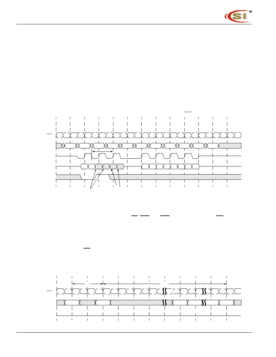
Data Strobe Preamble and Postamble Timings for DDR Read Cycles
Consecutive Burst Read Operation and Effects on the Data Strobe Preamble and Postamble
(CAS Latency = 2; Burst Length = 2)
T0
T1
T2
T3
T4
READ
NOP
NOP
NOP
D
0
D
1
CK, CK
Command
DQS
DQ
t
RPRE
(max)
t
RPST
(min)
t
RPRE
(min)
t
RPST
(max)
t
DQSQ
(max)
t
DQSQ
(min)
NOP
Read
B
NOP
NOP
NOP
NOP
Read
A
D0
A
D1
A
NOP
D2
A
D3
A
Command
DQS
DQ
Burst Read Operation (CAS Latency = 2; Burst Length = 4)
CK, CK
NOP
D0
B
D1
B
D2
B
D3
B
NOP
Read
B
NOP
NOP
NOP
NOP
Read
A
D0
A
D1
A
NOP
D2
A
D3
A
Command
DQS
DQ
Burst Read Operation (CAS Latency = 2; Burst Length = 4)
CK, CK
NOP
D0
B
D1
B
D2
B
D3
B
IC4
3R16160
Integrated Circuit Solution Inc.
11
DDR001-0B
11
/
10
/
2004
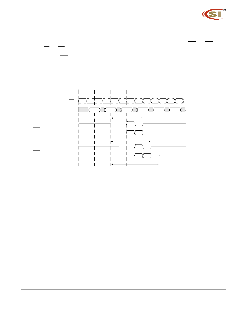
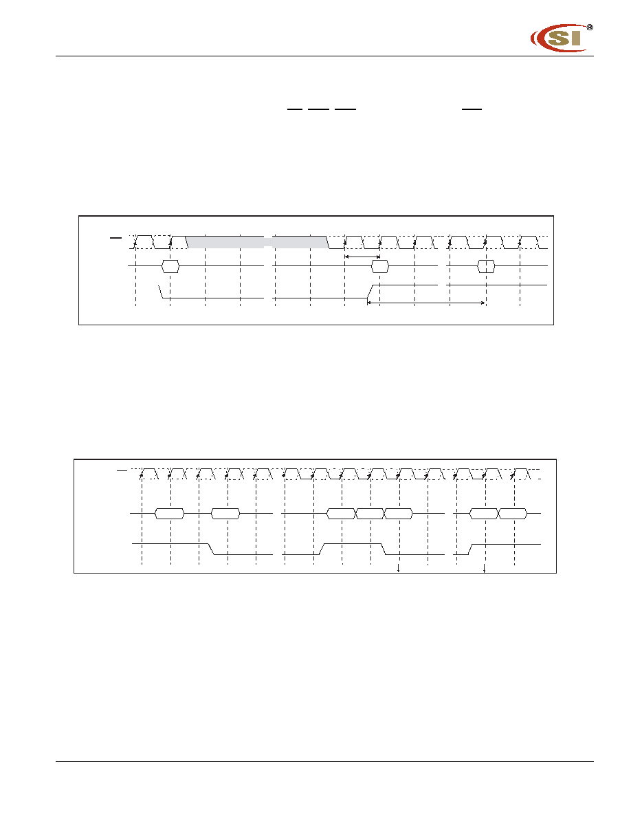
Auto Precharge Operation
The Auto Precharge operation can be issued by having column address A
10
high when a Read or Write
command is issued. If A
10
is low when a Read or Write command is issued, then normal Read or Write burst
operation is executed and the bank remains active at the completion of the burst sequence. When the Auto
Precharge command is activated, the active bank automatically begins to precharge at the earliest possible
moment during the Read or Write cycle once t
RAS
(min) is satisfied.
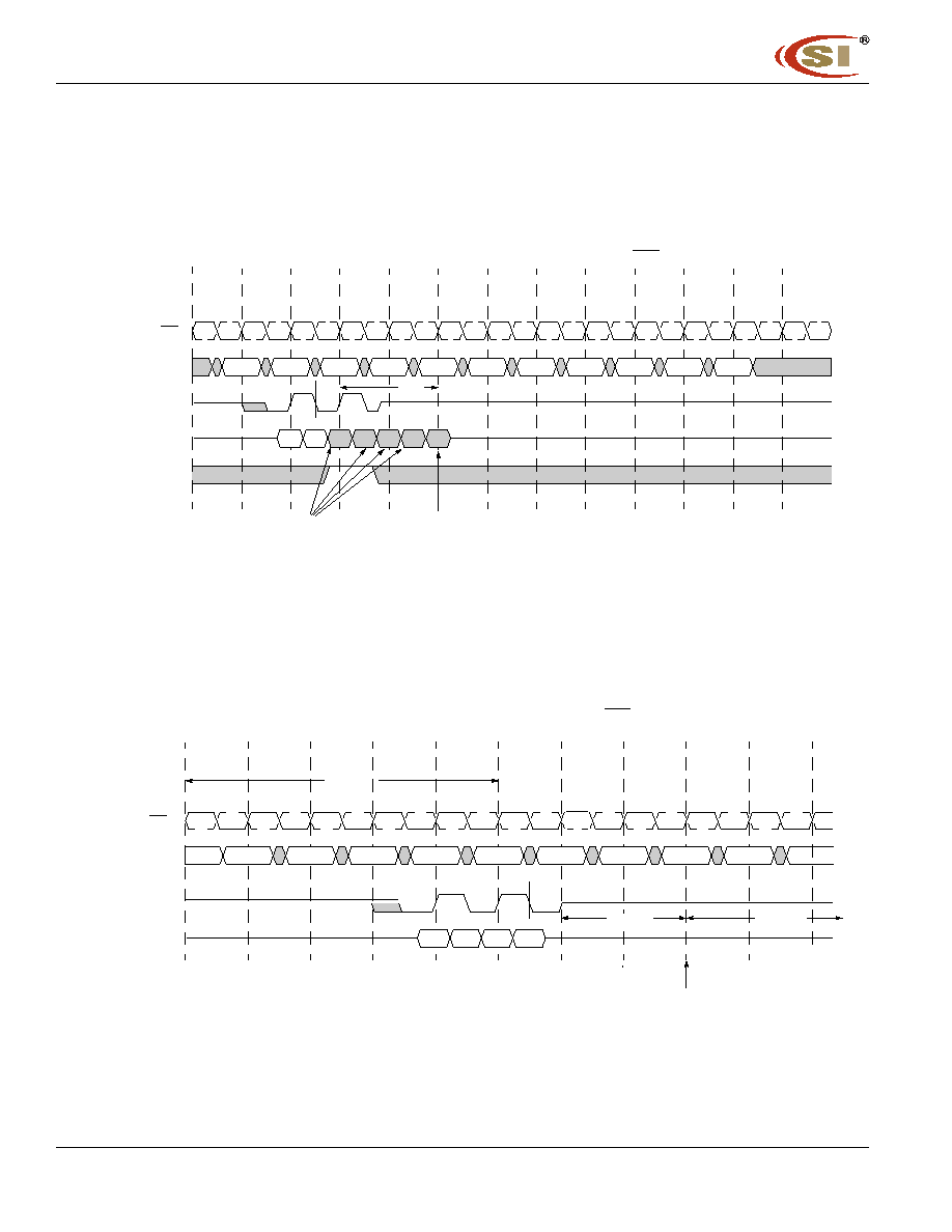
Read with Auto Precharge
If a Read with Auto Precharge command is initiated, the DDR SDRAM will enter the precharge operation
N-clock cycles measured from the last data of the burst read cycle where N is equal to the CAS latency pro-
grammed into the device. Once the autoprecharge operation has begun, the bank cannot be reactivated until
the minimum precharge time (t
RP
) has been satisfied.
Read with Autoprecharge Timing
(CAS Latency = 2; Burst Length = 4)
T0
T1
T2
T3
T4
T5
T6
T7
T8
D
0
D
1
D
2
D
3
Begin Autoprecharge
BA
ACT
R w/AP
NOP
NOP
NOP
NOP
NOP
NOP
CK, CK
Command
DQS
DQ
t
RAS
(min)
t
P
(min)
Earliest Bank A reactivate
T9
IC4
3R16160
12 Integrated Circuit Solution Inc.
DDR001
-
0B
11
/
10
/
2004
Read with Autoprecharge Timing as a Function of CAS Latency
T0
T1
T2
T3
T4
T5
T6
T7
T8
NOP
RAP
NOP
NOP
NOP
NOP
BA
NOP
CK, CK
Command
DQS
DQ
t
RAS
(min)
t
RP
(min)
BA
NOP
T9
D
0
D
1
D
2
D
3
DQS
DQ
CAS Latency=2
CAS Latency=2.5
(CAS Latency = 2, 2.5, Burst Length = 4)
D
0
D
1
D
2
D
3
IC4
3R16160
Integrated Circuit Solution Inc.
13
DDR001-0B
11
/
10
/
2004
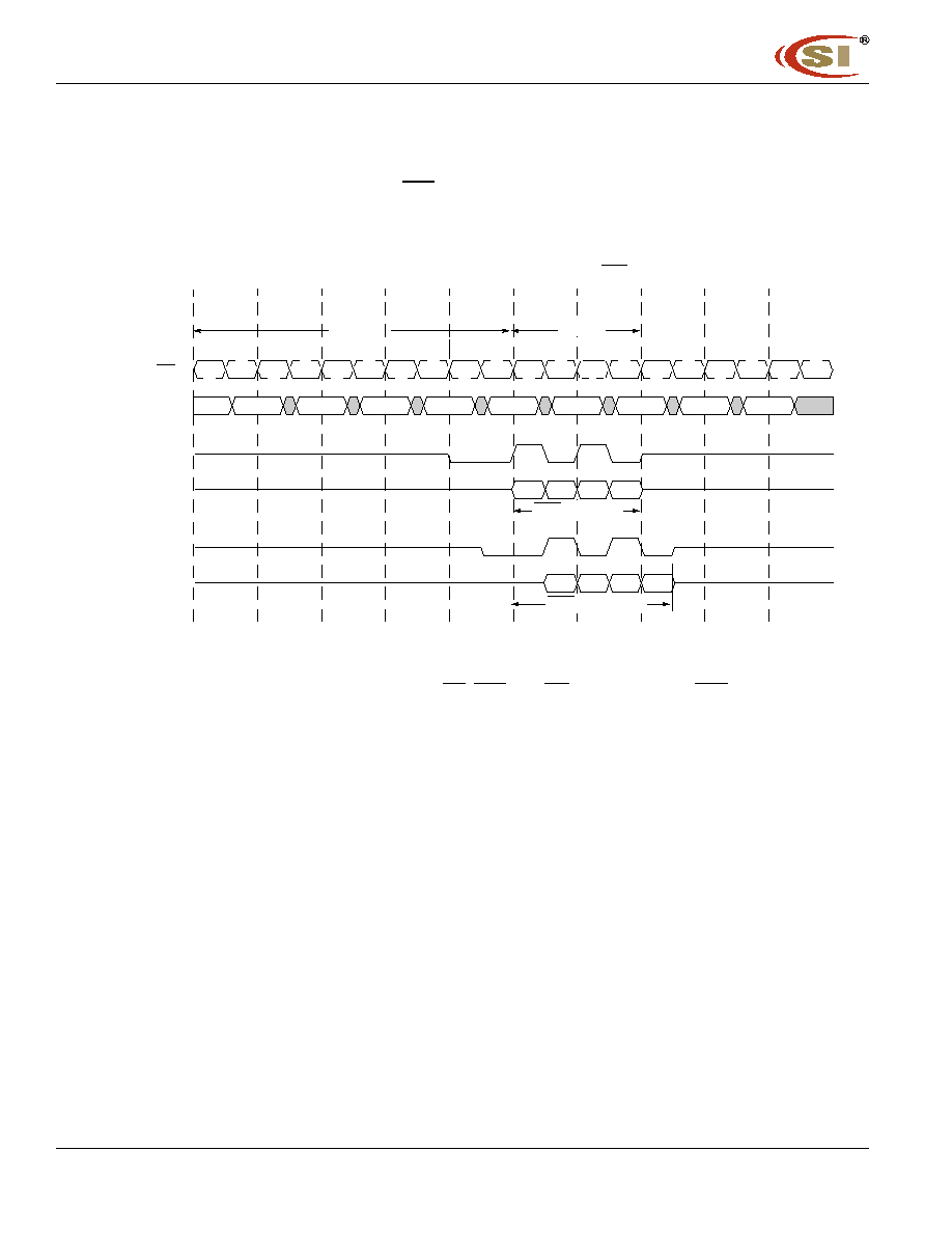
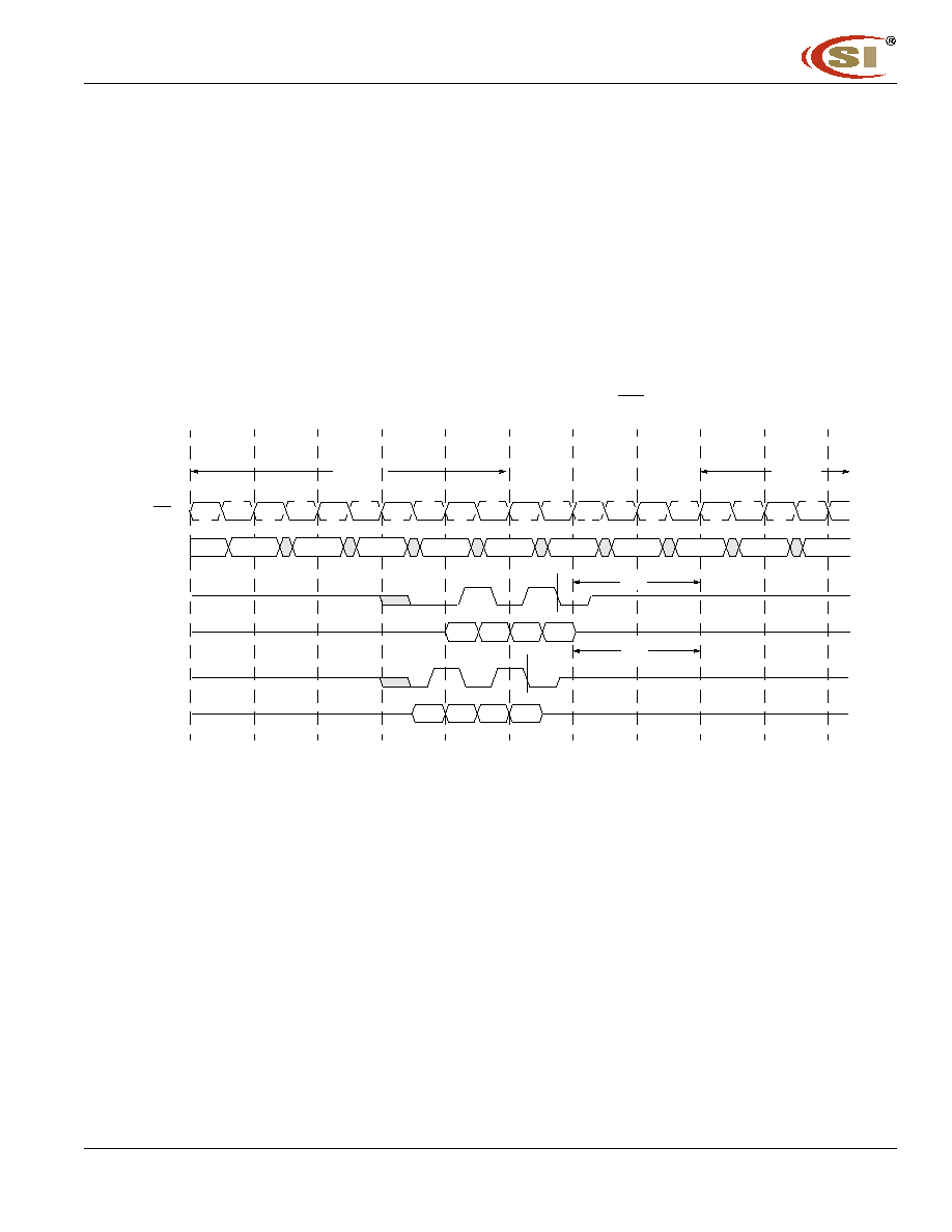
Precharge Timing During Read Operation
For the earliest possible Precharge command without interrupting a Read burst, the Precharge command
may be issued on the rising clock edge which is CAS latency (CL) clock cycles before the end of the Read
burst. A new Bank Activate (BA) command may be issued to the same bank after the RAS precharge time
(t
RP
). A Precharge command can not be issued until t
RAS
(min) is satisfied.
Read with Precharge Timing as a Function of CAS Latency
T0
T1
T2
T3
T4
T5
T6
T7
T8
D
0
D
1
D
2
D
3
NOP
Read
NOP
NOP
Pre
A
NOP
BA
NOP
CK, CK
Command
DQS
DQ
t
RAS
(min)
t
RP
(min)
BA
NOP
T9
D
0
D
1
D
2
D
3
DQS
DQ
CAS Latency=2
CAS Latency=2.5
(CAS Latency = 2, 2.5, 3; Burst Length = 4)
IC4
3R16160
14 Integrated Circuit Solution Inc.
DDR001
-
0B
11
/
10
/
2004
Burst Stop Command
The Burst Stop command is valid only during burst read cycles and is initiated by having RAS and CAS
high with CS and WE low at the rising edge of the clock. When the Burst Stop command is issued during a
burst Read cycle, both the output data (DQ) and data strobe (DQS) go to a high impedance state after a delay
(L
BST
) equal to the CAS latency programmed into the device. If the Burst Stop command is issued during a
burst Write cycle, the command will be treated as a NOP command.
Read Terminated by Burst Stop Command Timing
(CAS Latency = 2, 2.5, 3; Burst Length = 4)
T0
T1
T2
T3
T4
T5
T6
BST
NOP
NOP
NOP
NOP
Read
D
0
D
1
CK, CK
Command
DQS
DQ
D
0
D
1
DQS
DQ
CAS Latency = 2
CAS Latency = 2.5
L
BST
L
BST
L
BST
IC4
3R16160
Integrated Circuit Solution Inc.
15
DDR001-0B
11
/
10
/
2004
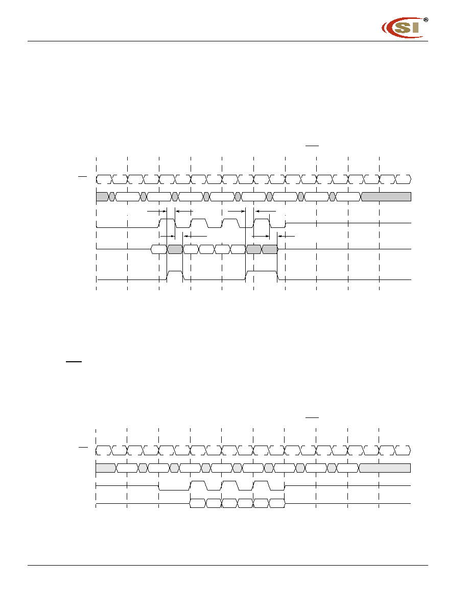
Read Interrupted by a Precharge
A Burst Read operation can be interrupted by a precharge of the same bank. The Precharge command to
Output Disable latency is equivalent to the CAS latency.
Read Interrupted by a Precharge Timing
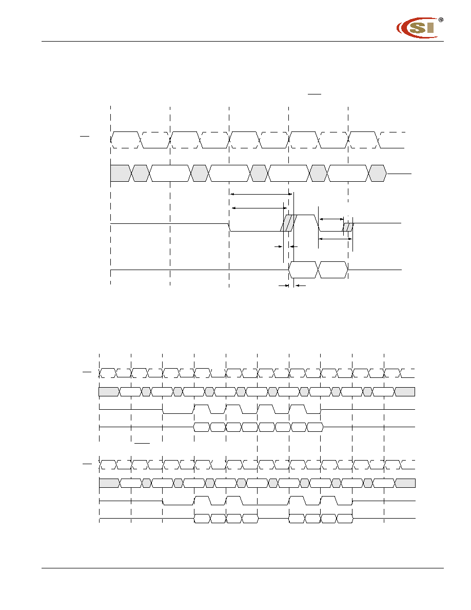
Burst Write Operation
The Burst Write command is issued by having CS, CAS, and WE low while holding RAS high at the rising
edge of the clock. The address inputs determine the starting column address. The memory controller is re-
quired to provide an input data strobe (DQS) to the DDR SDRAM to strobe or latch the input data (DQ) and
data mask (DM) into the device. During Write cycles, the data strobe applied to the DDR SDRAM is required
to be nominally centered within the data (DQ) and data mask (DM) valid windows. The data strobe must be
driven high nominally one clock after the write command has been registered. Timing parameters t
DQSS
(min)
and t
DQSS
(max) define the allowable window when the data strobe must be driven high.
Input data for the first Burst Write cycle must be applied one clock cycle after the Write command is
registered into the device (WL=1). The input data valid window is nominally centered around the midpoint of
the data strobe signal. The data window is defined by DQ to DQS setup time (t
QDQSS
) and DQ to DQS hold
time (t
QDQSH
). All data inputs must be supplied on each rising and falling edge of the data strobe until the burst
length is completed. When the burst has finished, any additional data supplied to the DQ pins will be ignored.
Write Preamble and Postamble Operation
Prior to a burst of write data and given that the controller is not currently in burst write mode, the data strobe
signal (DQS), must transition from Hi-Z to a valid logic low. This is referred to as the data strobe "write preamble".
This transition from Hi-Z to logic low nominally happens on the falling edge of the clock after the write com-
mand has been registered by the device. The preamble is explicitly defined by a setup time (t
WPRES
(min)) and
hold time (t
WPREH
(min)) referenced to the first falling edge of CK after the write command.
T0
T1
T2
T3
T4
T5
T6
T7
T8
D
0
D
1
D
2
D
3
NOP
Read
NOP
NOP
Pre
A
NOP
BA
NOP
CK, CK
Command
DQS
DQ
t
RAS
(min)
t
RP
(min)
BA
NOP
T9
D
0
D
1
D
2
D
3
DQS
DQ
CAS Latency=2
CAS Latency=2.5
(CAS Latency = 2, 2.5, 3; Burst Length = 8)
IC4
3R16160
16 Integrated Circuit Solution Inc.
DDR001
-
0B
11
/
10
/
2004
Burst Write Timing
Once the burst of write data is concluded and given that no subsequent burst write operations are initiated,
the data strobe signal (DQS) transitions from a logic low level back to Hi-Z. This is referred to as the data
strobe "write postamble". This transition happens nominally one-half clock period after the last data of the
burst cycle is latched into the device.
(CAS Latency = Any; Burst Length = 4)
T0
T1
T2
T3
T4
WRITE
NOP
NOP
NOP
D
0
D
1
D
2
D
3
CK, CK
Command
DQS(nom)
DQ(nom)
t
WPRES
t
WPREH
t
DQSS
t
WPST
t
QDQSH
D
0
D
1
D
2
D
3
DQS(min)
DQ(min)
t
DQSS
(min)
D
0
D
1
D
2
D
3
DQS(max)
DQ(max)
t
WPRES
(min)
t
DQSS
(max)
t
QDQSS
t
QDQSS
t
QDQSH
t
WPREH
(min)
t
WPREH
(max)
t
WPRES
(max)
IC4
3R16160
Integrated Circuit Solution Inc.
17
DDR001-0B
11
/
10
/
2004
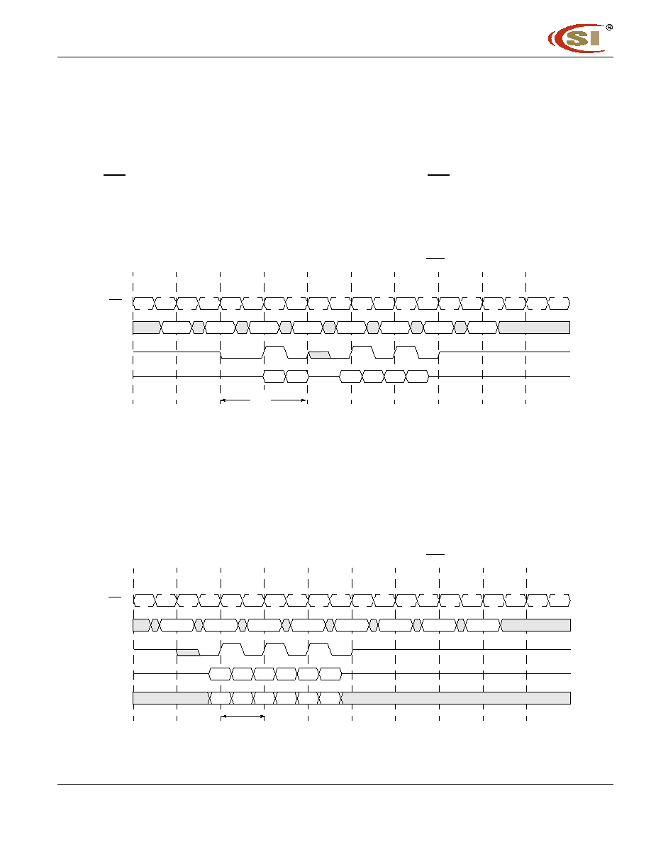
Write Interrupted by a Precharge
A Burst Write can be interrupted before completion of the burst by a Precharge command, with the only
restriction being that the interval that separates the commands be at least one clock cycle.
Write Interrupted by a Precharge Timing
Write with Auto Precharge
If A
10
is high when a Write command is issued, the Write with auto Precharge function is performed. Any
new command to the same bank should not be issued until the internal precharge is completed. The internal
precharge begins after keeping t
WR
(min.).
Write with Auto Precharge Timing
(CAS Latency = 2; Burst Length = 8)
T0
T1
T2
T3
T4
T5
T6
T7
T8
T9
T10
T11
Write
A
NOP
Pre
A
NOP
NOP
NOP
NOP
NOP
NOP
NOP
NOP
CK, CK
Command
DQS
T12
DM
D
0
D
1
D
2
D
3
DQ
Data is masked
by Precharge Command
Data is masked
by DM input
DQS input ignored
D
4
D
5
t
WR
D
6
(CAS Latency = Any; Burst Length = 4)
T0
T1
T2
T3
T4
T5
T6
T7
T8
D
0
D
1
D
2
D
3
NOP
WAP
NOP
NOP
NOP
NOP
NOP
NOP
BA
CK, CK
Command
DQS
DQ
t
RAS
(min)
t
RP
(min)
BA
NOP
T9
T10
t
WR
(min)
Begin Autoprecharge
IC4
3R16160
18 Integrated Circuit Solution Inc.
DDR001
-
0B
11
/
10
/
2004
Precharge Timing During Write Operation
Precharge timing for Write operations in DRAMs requires enough time to satisfy the write recovery require-
ment. This is the time required by a DRAM sense amp to fully store the voltage level. For DDR SDRAMs, a
timing parameter (t
WR
) is used to indicate the required amount of time between the last valid write operation
and a Precharge command to the same bank.
The "write recovery" operation begins on the rising clock edge after the last DQS edge that is used to strobe
in the last valid write data. "Write recovery" is complete on the next 2nd rising clock edge that is used to strobe
in the Precharge command.
Write with Precharge Timing
(CAS Latency = Any; Burst Length = 4)
T0
T1
T2
T3
T4
T5
T6
T7
T8
D
0
D
1
D
2
D
3
NOP
Write
NOP
NOP
NOP
NOP
Pre
A
NOP
CK, CK
Command
DQS
DQ
t
RAS
(min)
t
RP
(min)
BA
NOP
T9
T10
t
WR
D
0
D
1
D
2
D
3
DQS
DQ
t
WR
BA
IC4
3R16160
Integrated Circuit Solution Inc.
19
DDR001-0B
11
/
10
/
2004
Data Mask Function
The DDR SDRAM has a Data Mask function that is used in conjunction with the Write cycle, but not the
Read cycle. When the Data Mask is activated (DM high) during a Write operation, the Write is blocked (Mask
to Data Latency = 0).
When issued, the Data Mask must be referenced to both the rising and falling edges of Data Strobe.
Data Mask Timing
Burst Interruption
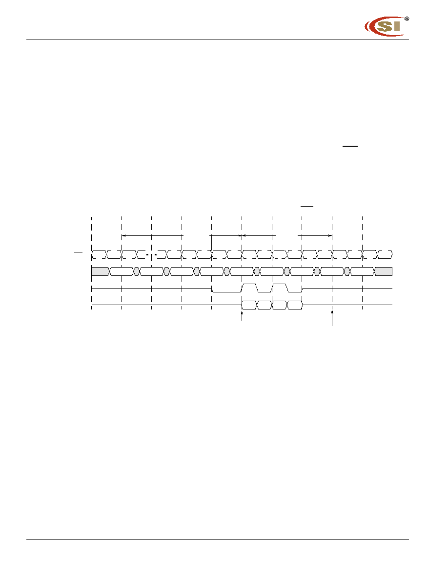
Read Interrupted by a Read
A Burst Read can be interrupted before completion of the burst by issuing a new Read command to any
bank. When the previous burst is interrupted, the remaining addresses are overridden with a full burst length
starting with the new address. The data from the first Read command continues to appear on the outputs until
the CAS latency from the interrupting Read command is satisfied. At this point, the data from the interrupting
Read command appears on the bus. Read commands can be issued on each rising edge of the system clock.
It is illegal to interrupt a Read with autoprecharge command with a Read command.
Read Interrupted by a Read Command Timing
(CAS Latency = Any; Burst Length = 8)
T0
T1
T2
T3
T4
T5
T6
T7
T8
D
0
D
1
D
2
D
3
D
4
D
5
D
6
D
7
NOP
NOP
NOP
NOP
NOP
NOP
NOP
Write
CK, CK
Command
DQS
DQ
DM
T9
t
DMDQSS
t
DMDQSS
t
DMDQSH
t
DMDQSH
(CAS Latency = 2; Burst Length = 4)
T0
T1
T2
T3
T4
T5
T6
T7
T8
Read
B
NOP
NOP
NOP
NOP
NOP
NOP
DA0 DA1 DB0 DB1
Read
A
DB2 DB3
CK, CK
Command
DQS
DQ
T9
IC4
3R16160
20 Integrated Circuit Solution Inc.
DDR001
-
0B
11
/
10
/
2004
Read Interrupted by a Write
To interrupt a Burst Read with a Write command, a Burst Stop command must be asserted to stop the burst
read operation and 3-state the DQ bus. Additionally, control of the DQS bus must be turned around to allow
the memory controller to drive the data strobe signal (DQS) into the DDR SDRAM for the write cycles. Once
the Burst Stop command has been issued, a Write command can not be issued until a minimum delay or
latency (L
BST
) has been satisfied. This latency is measured from the Burst Stop command and is equivalent
to the CAS latency programmed into the mode register. In instances where CAS latency is measured in half
clock cycles, the minimum delay (L
BST
) is rounded up to the next full clock cycle (i.e., if CL=2 then L
BST
=2, if
CL=2.5 then L
BST
=3). It is illegal to interrupt a Read with autoprecharge command with a Write command.
Read Interrupted by Burst Stop Command Followed by a Write Command Timing
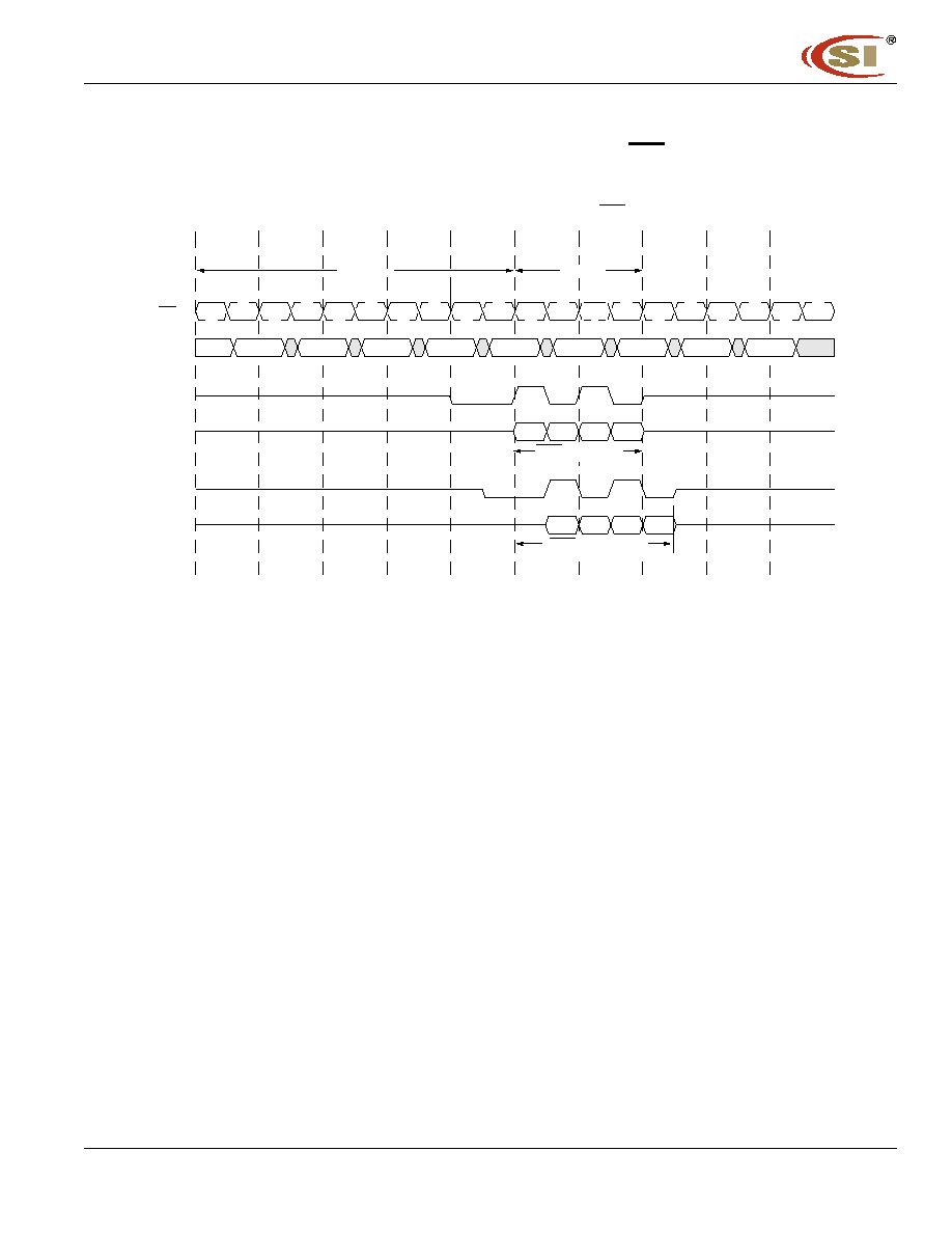
Write Interrupted by a Write
A Burst Write can be interrupted before completion by a new Write command to any bank. When the pre-
vious burst is interrupted, the remaining addresses are overridden with a full burst length starting with the new
address. The data from the first Write command continues to be input into the device until the Write Latency
of the interrupting Write command is satisfied (WL=1) At this point, the data from the interrupting Write com-
mand is input into the device. Write commands can be issued on each rising edge of the system clock. It is
illegal to interrupt a Write with autoprecharge command with a Write command.
Write Interrupted by a Write Command Timing
(CAS Latency = 2; Burst Length = 4)
T0
T1
T2
T3
T4
T5
T6
T7
T8
BST
NOP
Write
NOP
NOP
NOP
NOP
D
0
D
1
Read
D
0
D
1
D
2
D
3
CK, CK
Command
DQS
DQ
T9
L
BST
(CAS Latency = Any; Burst Length = 4)
T0
T1
T2
T3
T4
T5
T6
T7
T8
Write
A
NOP
NOP
Write
B
NOP
NOP
NOP
NOP
DA0 DA1 DB0 DB1 DB2 DB3
CK, CK
Command
DQS
DQ
DM
T9
Write Latency
DM0 DM1 DM0 DM1 DM2 DM3
IC4
3R16160
Integrated Circuit Solution Inc.
21
DDR001-0B
11
/
10
/
2004
Write Interrupted by a Read
A Burst Write can be interrupted by a Read command to any bank. If a burst write operation is interrupted
prior to the end of the burst operation, then the last two pieces of input data prior to the Read command must
be masked off with the data mask (DM) input pin to prevent invalid data from being written into the memory
array. Any data that is present on the DQ pins coincident with or following the Read command will be masked
off by the Read command and will not be written to the array. The memory controller must give up control of
both the DQ bus and the DQS bus at least one clock cycle before the read data appears on the outputs in
order to avoid contention. In order to avoid data contention within the device, a delay is required (t
CDLR
) from
the last valid data input before a Read command can be issued to the device. It is illegal to interrupt a Write
with autoprecharge command with a Read command.
Write Interrupted by a Read Command Timing
Auto Refresh
The Auto Refresh command is issued by having CS, RAS, and CAS held low with CKE and WE high at the
rising edge of the clock. All banks must be precharged and idle for a t
RP
(min) before the Auto Refresh com-
mand is applied. No control of the address pins is required once this cycle has started because of the internal
address counter. When the Auto Refresh cycle has completed, all banks will be in the idle state. A delay be-
tween the Auto Refresh command and the next Activate command or subsequent Auto Refresh command
must be greater than or equal to the t
RFC
(min). Commands may not be issued to the device once an Auto
Refresh cycle has begun. CS input must remain high during the refresh period or NOP commands must be
registered on each rising edge of the CK input until the refresh period is satisfied.
Auto Refresh Timing
(CAS Latency = 2; Burst Length = 8)
T0
T1
T2
T3
T4
T5
T6
T7
T8
T9
T10
T11
Write
NOP
Read
NOP
NOP
NOP
NOP
NOP
NOP
NOP
NOP
CK, CK
Command
DQS
T12
DM
D
2
D
3
D
4
D
5
D
0
D
2
D
3
D
4
D
5
D
6
D
1
D
7
DQ
Data is masked
by Read command
Data is masked
by DM input
DQS input ignored
D
0
D
1
t
WTR
T0
T1
T2
T3
T4
T5
T6
T7
T8
T9
T10
NOP
NOP
NOP
CK, CK
Command
CKE
T11
Auto Ref
ANY
High
Pre All
t
RFC
t
RP
IC4
3R16160
22 Integrated Circuit Solution Inc.
DDR001
-
0B
11
/
10
/
2004
Self Refresh
A self refresh command is defined by having CS, RAS, CAS and CKE held low with WE high at the rising
edge of the clock (CK). Once the self refresh command is initiated, CKE must be held low to keep the device
in self refresh mode. During the self refresh operation, all inputs except CKE are ignored. The clock is inter-
nally disabled during self refresh operation to reduce power consumption. The self refresh is exited by sup-
plying stable clock input before returning CKE high, asserting deselect or NOP command and then asserting
CKE high for longer than t
SREX
for locking of DLL. The auto refresh is required before self refresh entry and
after self refresh exit.
Power Down Mode
The power down mode is entered when CKE is low and exited when CKE is high. Once the power down
mode is initiated, all of the receiver circuits except clock, CKE and DLL circuit are gated off to reduce power
consumption. All banks should be in idle state prior to entering the precharge power down mode and CKE
should be set high at least 1tck+tIS prior to row active command. During power down mode, refresh opera-
tions cannot be performed, therefore the device cannot remain in power down mode longer than the refresh
period (t
REF
) of the device.
Command
CKE
Stable Clock
t
SREX
Auto
Refresh
NOP
Self
Refresh
� �
� �
� �
� �
� �
� �
CK, CK
� �
CKE
Precharge
Active
Read
NOP
Active
power down
power down
Exit
Active
Entry
power
Exit
down
power
Entry
down
Precharge
� �
� �
� �
� �
� �
� �
precharge
Command
CK, CK
IC4
3R16160
Integrated Circuit Solution Inc.
23
DDR001-0B
11
/
10
/
2004
TRUTH TABLE 1 � CKE
(Notes: 1-4)
NOTE:
1. CKE
n
is the logic state of CKE at clock edge n; CKE
n-1
was the state of CKE at the previous clock edge.
2. Current state is the state of the DDR SDRAM immediately prior to clock edge n.
3. COMMANDn is the command registered at clock edge n, and ACTIONn is a result of COMMANDn.
4. All states and sequences not shown are illegal or reserved.
5. DESELECT or NOP commands should be issued on any clock edges occurring during the
t
XSR period.
A minimum of 200 clock cycles is needed before applying a read command, for the DLL to lock.
CKEn-1 CKEn
CURRENT STATE
COMMANDn
ACTIONn
NOTES
L
L
Power-Down
X
Maintain Power-Down
Self Refresh
X
Maintain Self Refresh
L
H
Power-Down
DESELECT or NOP
Exit Power-Down
Self Refresh
DESELECT or NOP
Exit Self Refresh
5
H
L
All Banks Idle
DESELECT or NOP
Precharge Power-Down Entry
Bank(s) Active
DESELECT or NOP
Active Power-Down Entry
All Banks Idle
AUTO REFRESH
Self Refresh Entry
H
H
See Truth Table 3
IC4
3R16160
24 Integrated Circuit Solution Inc.
DDR001
-
0B
11
/
10
/
2004
TRUTH TABLE 2 � Current State Bank n - Command to Bank n
(Notes: 1-6; notes appear below and on next page)
NOTE:
1. This table applies when CKE
n-1
was HIGH and CKE
n
is HIGH (see Truth Table 2) and after
t
XSR
has been met (if the previous state was self refresh).
2. This table is bank-specific, except where noted, i.e., the current state is for a specific bank and the commands shown
are those allowed to be issued to that bank when in that state. Exceptions are covered in the notes below.
3. Current state definitions:
Idle: The bank has been precharged, and
t
RP has been met.
Row Active: A row in the bank has been activated, and
t
RCD has been met.
No data bursts/accesses and no register accesses are in progress.
Read: A READ burst has been initiated, with AUTO PRECHARGE disabled,
and has not yet terminated or been terminated.
Write: A WRITE burst has been initiated, with AUTO PRECHARGE disabled,
and has not yet terminated or been terminated.
4. The following states must not be interrupted by a command issued to the same bank. DESELECT or NOP com-
mands,
or allowable commands to the other bank should be issued on any clock edge occurring during these states.
Allowable commands to the other bank are determined by its current state and Truth Table 3, and according to
Truth Table 4.
Precharging: Starts with registration of a PRECHARGE command and ends when
t
RP is
met. Once
t
RP is met, the bank will be in the idle state.
CURRENT STATE
/CS
/RAS
/CAS
/WE
COMMAND/ACTION
NOTES
Any
H
X
X
X
DESELECT (NOP/continue previous operation)
L
H
H
H
NO OPERATION (NOP/continue previous operation)
Idle
L
L
H
H
ACTIVE (select and activate row)
L
L
L
H
AUTO REFRESH
7
L
L
L
L
MODE REGISTER SET
7
Row Active
L
H
L
H
READ (select column and start READ burst)
10
L
H
L
L
WRITE (select column and start WRITE burst)
10
L
L
H
L
PRECHARGE (deactivate row in bank or banks)
8
Read (Auto Precharge
Disabled)
L
H
L
H
READ (select column and start new READ burst)
10
L
L
H
L
PRECHARGE (truncate READ burst, start PRECHARGE)
8
L
H
H
L
BURST TERMINATE
9
Write (Auto Precharge
Disabled)
L
H
L
H
READ (select column and start READ burst)
10, 11
L
H
L
L
WRITE (select column and start new WRITE burst)
10
L
L
H
L
PRECHARGE (truncate WRITE burst, start PRECHARGE)
8, 11
IC4
3R16160
Integrated Circuit Solution Inc.
25
DDR001-0B
11
/
10
/
2004

NOTE: (continued)
Row Activating: Starts with registration of an ACTIVE command and ends when
t
RCD is
met. Once
t
RCD is met, the bank will be in the "row active" state.
Read w/Auto-Precharge Enabled: Starts with registration of a READ command with AUTO PRECHARGE
enabled and ends when
t
RP has been met. Once
t
RP is met, the bank will
be in the idle state.
Write w/Auto-Precharge Enabled: Starts with registration of a WRITE command with AUTO PRECHARGE
enabled and ends when
t
RP has been met. Once
t
RP is met, the bank will
be in the idle state.
5. The following states must not be interrupted by any executable command; DESELECT or NOP commands must be
applied on each positive clock edge during these states.
Refreshing: Starts with registration of an AUTO REFRESH command and ends when
t
RC is met. Once
t
RFC is met, the DDR SDRAM will be in the "all banks
idle" state.
Accessing Mode Register: Starts with registration of a MODE REGISTER SET command and ends
when
t
MRD has been met. Once
t
MTC is met, the DDR SDRAM will be in
the "all banks idle" state.
Precharging All: Starts with registration of a PRECHARGE ALL command and ends when
t
RP is met. Once
t
RP is met, all banks will be in the idle state.
6. All states and sequences not shown are illegal or reserved.
7. Not bank-specific; requires that all banks are idle and no bursts are in progress.
8. May or may not be bank-specific; if multiple banks are to be precharged, each must be in a valid state for precharging.
9. Not bank-specific; BURST TERMINATE affects the most recent READ burst, regardless of bank.
10. READs or WRITEs listed in the Command/Action column include READs or WRITEs with AUTO PRECHARGE
enabled and READs or WRITEs with AUTO PRECHARGE disabled.
11. Requires appropriate DM masking.
IC4
3R16160
26 Integrated Circuit Solution Inc.
DDR001
-
0B
11
/
10
/
2004
TRUTH TABLE 3 � Current State Bank n - Command to Bank m
(Notes: 1-6; notes appear below and on next page)
NOTE:
1. This table applies when CKE
n-1
was HIGH and CKE
n
is HIGH (see Truth Table 2) and after
t
XSR has been met
(if the previous state was self refresh).
2. This table describes alternate bank operation, except where noted, i.e., the current state is for bank n and the
commands shown are those allowed to be issued to bank m (assuming that bank m is in such a state that the given
command is allowable). Exceptions are covered in the notes below.
3. Current state definitions:
Idle: The bank has been precharged, and
t
RP has been met.
Row Active: A row in the bank has been activated, and
t
RCD has been met. No data
bursts/accesses and no register accesses are in progress.
Read: A READ burst has been initiated, with AUTO PRECHARGE disabled, and
has not yet terminated or been terminated.
Write: A WRITE burst has been initiated, with AUTO PRECHARGE disabled, and
has not yet terminated or been terminated.
CURRENT STATE
/CS
/RAS /CAS
/WE
COMMAND/ACTION
NOTES
Any
H
X
X
X
DESELECT (NOP/continue previous operation)
L
H
H
H
NO OPERATION (NOP/continue previous operation)
Idle
X
X
X
X
Any Command Otherwise Allowed to Bank m
Row Activating,
Active, or Precharging
L
L
H
H
ACTIVE (select and activate row)
L
H
L
H
READ (select column and start READ burst)
7
L
H
L
L
WRITE (select column and start WRITE burst)
7
L
L
H
L
PRECHARGE
Read
(Auto-Precharge
Disabled)
L
L
H
H
ACTIVE (select and activate row)
L
H
L
H
READ (select column and start new READ burst)
7
L
L
H
L
PRECHARGE
Write
(Auto- Precharge
Disabled)
L
L
H
H
ACTIVE (select and activate row)
L
H
L
H
READ (select column and start READ burst)
7, 8
L
H
L
L
WRITE (select column and start new WRITE burst)
7
L
L
H
L
PRECHARGE
Read
(With Auto-Precharge)
L
L
H
H
ACTIVE (select and activate row)
L
H
L
H
READ (select column and start new READ burst)
3a, 7
L
H
L
L
WRITE (select column and start WRITE burst)
3a, 7, 9
L
L
H
L
PRECHARGE
Write
(With Auto-Precharge)
L
L
H
H
ACTIVE (select and activate row)
L
H
L
H
READ (select column and start READ burst)
3a, 7
L
H
L
L
WRITE (select column and start new WRITE burst)
3a, 7
L
L
H
L
PRECHARGE
IC4
3R16160
Integrated Circuit Solution Inc.
27
DDR001-0B
11
/
10
/
2004

NOTE: (continued)
Read with Auto Precharge Enabled: See following text
Write with Auto Precharge Enabled: See following text
3a. The Read with Auto Precharge Enabled or Write with Auto Precharge Enabled states can each be broken
into two parts: the access period and the precharge period. For Read with Auto Precharge, the precharge
period is defined as if the same burst was executed with Auto Precharge disabled and then followed with the
earliest possible PRECHARGE command that still accesses all of the data in the burst. For Write with Auto
Precharge, the precharge period begins when tWR ends, with tWR measured as if Auto Precharge was
disabled. The access period starts with registration of the command and ends where the precharge period
(or
t
RP) begins.
During the precharge period of the Read with Auto Precharge Enabled or Write with Auto Precharge Enabled
states, ACTIVE, PRECHARGE, READ and WRITE commands to the other bank may be applied; during the
access period, only ACTIVE and PRECHARGE commands to the other bank may be applied. In either case, all
other related limitations apply (e.g. contention between READ data and WRITE data must be avoided).
4. AUTO REFRESH and MODE REGISTER SET commands may only be issued when all banks are idle.
5. A BURST TERMINATE command cannot be issued to another bank; it applies to the bank represented by the
current state only.
6. All states and sequences not shown are illegal or reserved.
7. READs or WRITEs listed in the Command/Action column include READs or WRITEs with AUTO PRECHARGE
enabled and READs or WRITEs with AUTO PRECHARGE disabled.
8. Requires appropriate DM masking.
9. A WRITE command may be applied after the completion of data output.
IC4
3R16160
28 Integrated Circuit Solution Inc.
DDR001
-
0B
11
/
10
/
2004
Simplified State Diagram
PREALL = Precharge All Banks
CKEL = Enter Power Down
MRS = Mode Register Set
CKEH = Exit Power Down
EMRS = Extended Mode Register Set
ACT = Active
REFS = Enter Self Refresh
Write A = Write with Autoprecharge
REFSX = Exit Self Refresh
Read A = Read with Autoprecharge
REFA = Auto Refresh
PRE = Precharge
Self
Auto
Idle
MRS
EMRS
Row
Precharge
Write
Write
Write
Read
Read
Power
ACT
Read A
Read
REFS
REFSX
REFA
CKEL
MRS
CKEH
CKEH
CKEL
Write
Power
Applied
Automatic Sequence
Command Sequence
Read A
Write A
Read
PRE
PRE
PRE
PRE
Refresh
Refresh
Active
Active
Power
Down
Precharge
Power
Down
On
A
Read
A
Read
A
Write A
Burst Stop
PREALL
Precharge
PREALL
IC4
3R16160
Integrated Circuit Solution Inc.
29
DDR001-0B
11
/
10
/
2004
DC Operating Conditions & Specifications
DC Operating Conditions
Recommended operating conditions(Voltage referenced to VSS=0V, TA=0 to 70�C)
Notes: 1. V
REF
is expected to be equal to 0.5*V
DDQ
of the transmitting device, and to track variations in the DC level of the same. Peak-
to-peak noise on V
REF
may not exceed 2% of the DC value
2.V
TT
is not applied directly to the device. V
TT
is a system supply for signal termination resistors, is expected to be set equal to
V
REF
, and must track variations in the DC level of V
REF
3. V
ID
is the magnitude of the difference between the input level on CK and the input level on CK.
Table 11. DC operating condition
Parameter
Symbol
Min
Max
Unit
Note
Supply voltage (for device with a nominal V
DD
of 2.5V)
V
DD
2.3
2.7
Supply voltage (V
DD
of 2.6V for DDR400 device)
V
DD
2.5
2.7
I/O Supply voltage
V
DDQ
2.3
2.7
V
I/O Supply voltage for DDR400 device
V
DDQ
2.5
2.7
V
I/O Reference voltage
V
REF
0.49*VDDQ
0.51*VDDQ
V
1
I/O Termination voltage(system)
V
TT
V
REF
-0.04
V
REF
+0.04
V
2
Input logic high voltage
V
IH
(DC)
V
REF
+0.15
V
DDQ
+0.3
V
Input logic low voltage
V
IL
(DC)
-0.3
V
REF
-0.15
V
Input Voltage Level, CK and CK inputs
V
IN
(DC)
-0.3
V
DDQ
+0.3
V
Input Differential Voltage, CK and CK inputs
V
ID
(DC)
0.3
V
DDQ
+0.6
V
3
Input leakage current
I
I
-2
2
uA
Output leakage current
I
OZ
-5
5
uA
Output High Current (V
OUT
= 1.95V)
I
OH
-16.8
mA
Output Low Current (V
OUT
= 0.35V)
I
OL
16.8
mA
IC4
3R16160
30 Integrated Circuit Solution Inc.
DDR001
-
0B
11
/
10
/
2004
IDD Max Specifications and Conditions
(0�C < TA < 70�C, VDDQ=2.5V+ 0.2V, VDD=2.5 +0.2V, for DDR400 device VDDQ=2.6V+ 0.1V, VDD=2.6 +0.1V
Symbol
-5
-6
-7
Unit
Operating current - One bank Active-Precharge; tRC=tRCmin;tCK=133Mhz for
DDR266, 166Mhz for DDR333; DQ,DM and DQS inputs chang-ing twice per clock
cycle; address and control inputs changing once per clock cycle
IDD0
120
110
100
mA
Operating current - One bank operation; One bank open, BL=4
IDD1
160
140
120
mA
Percharge power-down standby current; All banks idle; power - down mode; CKE
=< VIL(max); tCK=133Mhz for DDR266; Vin = Vref for DQ,DQS and DM
IDD2P
30
25
20
mA
Precharge Floating standby current; CS# > =VIH(min);All banks idle; CKE > =
VIH(min); tCK=133Mhz for DDR266; Address and other control inputs changing once
per clock cycle; Vin = Vref for DQ,DQS and DM
IDD2F
52
45
38
mA
Precharge Quiet standby current; CS# > = VIH(min); All banks idle; CKE > =
VIH(min); tCK =133Mhz for DDR266; Address and other control inputs stable with
keeping >= VIH(min) or =<VIL(max); Vin = Vref for DQ ,DQS and DM
IDD2Q
50
44
37
mA
Active power - down standby current; one bank active; power-down mode; CKE=<
VIL (max); tCK =133Mhz for DDR266, 166MHZ for DDR333; Vin = Vref for DQ,DQS
and DM
IDD3P
30
25
20
mA
Active standby current; CS# >= VIH(min); CKE>=VIH(min); one bank active; active -
precharge; tRC=tRASmax; tCK =133Mhz for DDR266, 166Mhz for DDR333; DQ, DQS
and DM inputs changing twice per clock cycle; address and other control inputs
changing once per clock cycle
IDD3N
90
80
70
mA
Operating current - burst read; Burst length = 2; reads; continguous burst; One bank
active; address and control inputs changing once per clock cycle; CL=2 at tCK =
133Mhz for DDR266, CL=2.5 at tCK=166Mhz for DDR333; 50% of data changing at
every burst; lout = 0 m A
IDD4R
270
230
190
mA
Operating current - burst write; Burst length = 2; writes; continuous burst; One bank
active address and control inputs changing once per clock cycle; CL=2 at tCK =
133Mhz for DDR266 ; DQ, DM and DQS inputs changing twice per clock cycle, 50% of
input data changing at every burst
IDD4W
250
210
170
mA
Auto refresh current; tRC = tRFC(min) - 10*tCK for DDR266 at 133Mhz, 12*tCK for
DDR333; distributed refresh
IDD5
210
200
190
mA
Self refresh current; CKE =< 0.2V; External clock should be on; tCK =133Mhz for
DDR266, 166Mhz for DDR333.
IDD6
(nomal)
3
3
3
mA
Self refresh current; (Low Power)
(L)
1.8
1.8
1.8
mA
Operating current - Four bank operation; Four bank interleaving with BL=4
IDD7
400
350
300
mA
Conditions
Version
IC4
3R16160
Integrated Circuit Solution Inc.
31
DDR001-0B
11
/
10
/
2004
AC Operating Conditions & Timming Specification
AC Operating Conditions
Note:
1.Vih(max) = 4.2V. The overshoot voltage duration is < 3ns at VDD.
2. Vil(min) = -1.5V. The undershoot voltage duration is < 3ns at VSS.
3. VID is the magnitude of the difference between the input level on CK and the input on CK.
4. The value of V
IX
is expected to equal 0.5*V
DDQ
of the transmitting device and must track variations in the DC level of the same.
ELECTRICAL CHARACTERISTICS AND AC TIMING for PC400/PC333/PC266/PC200 -Abso-
lute Specifications
(Notes: 1-5, 14-17) (0�C < T
A
< 70�C; V
DD
Q = +2.5V �0.2V, +2.5V �0.2V for DDR400 device V
DD
Q = +2.6V �0.1V, +2.5V
�0.1V)
Parameter/Condition
Symbol
Min
Max
Unit
Note
Input High (Logic 1) Voltage, DQ, DQS and DM signals
VIH(AC)
VREF + 0.31
V
1
Input Low (Logic 0) Voltage, DQ, DQS and DM signals.
VIL(AC)
VREF - 0.31
V
2
Input Differential Voltage, CK and CK inputs
VID(AC)
0.7
VDDQ+0.6
V
3
Input Crossing Point Voltage, CK and CK inputs
VIX(AC)
0.5*VDDQ-0.2
0.5*VDDQ+0.2
V
4
SYMBOL
MIN
MAX
MIN
MAX
MIN
MAX
UNITS
NOTES
t
AC
-0.65
0.65
-0.7
0.7
-0.75
0.75
ns
CK high-level width
T
CH
0.45
0.55
0.45
0.55
0.45
0.55
t
CK
30
CK low-level width
T
CL
0.45
0.55
0.45
0.55
0.45
0.55
t
CK
30
Clock cycle time
CL = 3
t
CK(3)
5
10
-
12
-
12
ns
48
CL = 2.5
t
CK(2.5)
6
10
6
12
7
12
ns
48
CL = 2.5
t
CK(2)
7.5
10
7.5
12
7.5
12
ns
48
t
DH
0.40
0.45
0.50
ns
26,31
t
DS
0.40
0.45
0.50
ns
26,31
t
DIPW
1.75
1.75
1.75
ns
31
t
DQSCK
-0.6
0.6
-0.6
0.6
-0.75
0.75
ns
t
DQSH
0.35
0.35
0.35
t
CK
t
DQSL
0.35
0.35
0.35
t
CK
t
DQSQ
0.4
0.45
0.5
ns
25,26
t
DQSS
0.72
1.25
0.75
1.25
0.75
1.25
t
CK
t
DSS
0.2
0.2
0.2
t
CK
-5
-6
-7
Access window of DQs from CK/
CK
DQ and DM input hold time relative
to DQS
DQ and DM input setup time
relative to DQS
DQ and DM input pulse width (for
each input)
Access window of DQS from
CK/
CK
DQS input high pulse width
DQS input low pulse width
DQS-DQ skew, DQS to last DQ
valid, per group, per access
Write command to first DQS
latching transition
DQS falling edge to CK rising -
setup time
AC CHARACTERISTICS
PARAMETER
IC4
3R16160
32 Integrated Circuit Solution Inc.
DDR001
-
0B
11
/
10
/
2004

AC CHARACTERISTICS
PARAMETER
SYMBOL
MIN
MAX
MIN
MAX
MIN
MAX
UNITS
NOTES
DQS falling edge from CK rising -
hold time
t
DSH
0.2
0.2
0.2
0.75
t
CK
t
CH
t
CH
t
CH
t
CL
t
CL
t
CL
Data-out high-impedance window
from CK/
CK
t
HZ
-0.65
0.65
-0.7
0.7
-0.75
0.75
ns
18
Data-out low-impedance window
from CK/
CK
t
LZ
-0.65
0.65
-0.7
0.7
-0.75
0.75
ns
18
Address and control input hold
time (fast slew rate)
t
IH
F
0.6
0.75
0.9
ns
14
Address and control input setup
time (fast slew rate)
t
IS
F
0.6
0.75
0.9
ns
14
Address and control input hold
time (slow slew rate)
t
IH
s
0.7
0.8
1
ns
14
Address and control input setup
time (slow slew rate)
t
IS
s
0.7
0.8
1
ns
14
LOAD MODE REGISTER
command cycle time
t
MRD
2.00
2.00
2.00
t
CK
DQ-DQS hold, DQS to first DQ to
t
HP
t
HP
t
HP
non-valid,per access
-
t
QHS
-
t
QHS
-
t
QHS
Data hold skew factor
t
QHS
0.5
0.6
0.75
ns
ACTIVE to PRECHARGE com-
mand
t
RAS
40
70,000
42
120,000
45
120,000
ns
35
ACTIVE to READ with Auto pre-
charge command
t
RAP
ns
43
ACTIVE to ACTIVE/AUTO RE-
FRESH command period
t
RC
60
60
65
ns
AUTO REFRESH command period
t
RFC
70
72
75
ns
46
ACTIVE to READ or WRITE delay
t
RCD
15
18
15
ns
PRECHARGE command period
t
RP
15
18
15
ns
DQS read preamble
t
RPRE
0.9
1.1
0.9
1.1
0.9
1.1
t
CK
DQS read postamble
t
RPST
0.4
0.6
0.4
0.6
0.4
0.6
t
CK
ACTIVE bank a to ACTIVE bank b
command
t
RRD
10
12
15
ns
DQS write preamble
t
WPRE
0.25
0.25
0.25
t
CK
DQS write preamble setup time
t
WPRES
0
0
0
ns
20,21
-7
25,26
Half clock period
t
HP
-5
-6
t
RAS(MIN) - (burst length *
t
CK/2)
34
ns
t
QH
ns
IC4
3R16160
Integrated Circuit Solution Inc.
33
DDR001-0B
11
/
10
/
2004
AC CHARACTERISTICS
PARAMETER
SYMBOL
MIN
MAX
MIN
MAX
MIN
MAX
UNITS
NOTES
DQS write postamble
t
WPST
0.4
0.6
0.4
0.4
t
CK
19
Write recovery time
t
WR
15
15
15
ns
Internal WRITE to READ
command delay
t
WTR
2
2
2
t
CK
Average periodic refresh interval
t
REFI
7.8
7.8
7.8
us
Terminating voltage delay to VDD
t
VTD
0
0
0
ns
Exit SELF REFRESH to non-
READ command
t
XSNR
200
200
200
t
CK
t
QH -
t
DQSQ
Data valid output window
na
ns
25
-7
-5
-6
t
QH -
t
DQSQ
t
QH -
t
DQSQ
IC4
3R16160
34 Integrated Circuit Solution Inc.
DDR001
-
0B
11
/
10
/
2004
SLEW RATE DERATING VALUES
(Notes: 14; notes appear on page 36) 0�C T
A
+70�C; V
DDQ
= +2.5V �0.2V, V
DD
= +2.5V �0.2V for
DDR400 V
DDQ
= +2.6V �0.1V, V
DD
= +2.6V �0.1V)
SLEW RATE DERATING VALUES
(Note: 31; notes appear on page 37) (0�C T
A
+70�C; V
DDQ
= +2.5V �0.2V, V
DD
= +2.5V �0.2V for
DDR400 V
DDQ
= +2.6V �0.1V, V
DD
= +2.6V �0.1V)
NOTES:
1. All voltages referenced to VSS.
2. Tests for AC timing, IDD, and electrical AC and DC characteristics may be conducted at nominal
reference/supply voltage levels, but the related specifications and device operation are guaranteed for the
full voltage range specified.
ADDRESS / COMMAND
SLEW RATE
t
IS
t
IH UNITS
NOTES
0.500V / ns
0
0
ps
14
0.400V / ns
+50
+50
ps
14
0.300V / ns
+100
+100
ps
14
0.200V / ns
+150
+150
ps
14
Date, DQS, DM
SLEW RATE
t
DS
t
DH
UNITS
NOTES
0.500V / ns
0
0
ps
31
0.400V / ns
+75
+75
ps
31
0.300V / ns
+150
+150
ps
31
0.200V / ns
+225
+225
ps
31
IC4
3R16160
Integrated Circuit Solution Inc.
35
DDR001-0B
11
/
10
/
2004

3. Outputs measured with equivalent load:
NOTES: (continued)
4. AC timing and IDD tests may use a VIL-to-VIH swing of up to 1.5V in the test environment, but input
timing is still referenced to VREF (or to the crossing point for CK/CK), and parameter specifications
are guaranteed for the specified AC input levels under normal use conditions. The minimum slew rate
for the input signals used to test the device is 1V/ns in the range between VIL(AC) and VIH(AC).
5. The AC and DC input level specifications are as defined in the SSTL_2 Standard (i.e., the receiver will
effectively switch as a result of the signal crossing the AC input level, and will remain in that state as long
as the signal does not ring back above [below] the DC input LOW [HIGH] level).
6. VREF is expected to equal VDDQ/2 of the transmit-ting device and to track variations in the DC level
of the same. Peak-to-peak noise (non-common mode) on VREF may not exceed �2 percent of the DC value.
Thus, from VDDQ/2, VREF is allowed �25mV for DC error and an additional �25mV for AC noise.
7. VTT is not applied directly to the device. VTT is a system supply for signal termination resistors, is expected
to be set equal to VREF and must track variations in the DC level of VREF.
8. VID is the magnitude of the difference between the input level on CK and the input level on CK.
9. The value of VIX is expected to equal VDDQ/2 of the transmitting device and must track varia-tions in the
DC level of the same.
10. IDD is dependent on output loading and cycle rates. Specified values are obtained with minimum cycle
time at CL = 2 for -6, -7 .
11. Enables on-chip refresh and address counters.
12. IDD specifications are tested after the device is properly initialized, and is averaged at the defined cycle rate.
13. This parameter is sampled. VDD = +2.5V �0.2V, VDDQ = +2.5V �0.2V, VREF = VSS, f = 100 MHz, T A = 25�C,
VOUT(DC) = VDDQ/2, VOUT (peak to peak) = 0.2V. DM input is grouped with I/O pins, reflecting the fact that they
are matched in loading.
14. Command/Address input slew rate = 0.5V/ns. For -5, -6, -7 and -75 with slew rates 1V/ns and faster,
t
IS and
t
IH
are reduced to 900ps. If the slew rate is less than 0.5V/ns, timing must be derated:
t
IS and
t
IH has an additional 50ps
per each 100mV/ns reduction in slew rate from the 500mV/ns. If the slew rate exceeds 4.5V/ns, functionality is un-
certain.
15. The CK/CK input reference level (for timing referenced to CK/CK) is the point at which CK and CK cross; the input
reference level for signals other than CK/CK is VREF.
16. Inputs are not recognized as valid until VREF stabilizes. Exception: during the period before VREF stabilizes,
CKE �0.3 x VDDQ is recognized as LOW.
17. The output timing reference level, as measured at the timing reference point indicated in Note 3, is VTT.
18.
t
HZ and
t
LZ transitions occur in the same access time windows as valid data transitions. These parameters
are not referenced to a specific voltage level, but specify when the device output is no longer driving (HZ) or begins
driving (LZ).
19. The maximum limit for this parameter is not a device limit. The device will operate with a greater value for this
Output
(V
OUT
)
V
TT
50
Reference
Point
30pF
IC4
3R16160
36 Integrated Circuit Solution Inc.
DDR001
-
0B
11
/
10
/
2004

parameter, but system performance (bus turnaround) will degrade accordingly.
20. This is not a device limit. The device will operate with a negative value, but system performance could be
degraded due to bus turnaround.
21. It is recommended that DQS be valid (HIGH or LOW) on or before the WRITE command. The case shown (DQS
going from High-Z to logic LOW) applies when no WRITEs were previously in progress on the bus. If a previous
WRITE was in progress, DQS could be HIGH during this time, depending on
t
DQSS.
22. MIN (
t
RC or
t
RFC) for IDD measurements is the smallest multiple of
t
CK that meets the minimum absolute value
for the respective parameter.
t
RAS (MAX) for IDD measurements is the largest multiple of
t
CK that
meets the maximum absolute value for
t
RAS.
NOTES: (continued)
23. The refresh period 64ms. This equates to an average refresh rate of 7.8�s.
24. The I/O capacitance per DQS and DQ byte/group will not differ by more than this maximum amount for any
given device.
25. The valid data window is derived by achieving other specifications -
t
HP (
t
CK/2),
t
DQSQ, and
t
QH
(
t
QH =
t
HP -
t
QHS). The data valid window derates directly porportional with the clock duty cycle and a practical data
valid window can be derived. The clock is allowed a maximum duty cycle variation of 45/55. Functionality is uncertain
when operating beyond a 45/55 ratio.
26. Referenced to x16 = LDQS with DQ0-DQ7; and UDQS with DQ8-DQ15.
27. This limit is actually a nominal value and does not result in a fail value. CKE is HIGH during REFRESH command
period (
t
RFC [MIN]) else CKE is LOW (i.e., during standby).
28. To maintain a valid level, the transitioning edge of the input must:
a) Sustain a constant slew rate from the current AC level through to the target AC level, VIL(AC) or VIH(AC).
b) Reach at least the target AC level.
c) After the AC target level is reached, continue to maintain at least the target DC level, VIL(DC) or VIH(DC).
29. The Input capacitance per pin group will not differ by more than this maximum amount for any given device..
30. CK and CK input slew rate must be �1V/ns.
31. DQ and DM input slew rates must not deviate from DQS by more than 10%. If the DQ/DM/DQS slew rate is less
than 0.5V/ns, timing must be derated: 50ps must be added to
t
DS and
t
DH for each 100mv/ns reduction in slew rate.
If slew rate exceeds 4V/ns, functionality is uncertain.
IC4
3R16160
Integrated Circuit Solution Inc.
37
DDR001-0B
11
/
10
/
2004

NOTES: (continued)
33. The clock is allowed up to �150ps of jitter. Each timing parameter is allowed to vary by the same amount.
34.
t
HP min is the lesser of
t
CL minimum and
t
CH minimum actually applied to the device CK and CK/ inputs,
collectively during bank active.
35. READs and WRITEs with auto precharge are not allowed to be issued until
t
RAS(MIN) can be satisfied prior
to the internal precharge com-mand being issued.
36. Applies to x16. First DQS (LDQS or UDQS) to transition to last DQ (DQ0-DQ15) to transition valid.
Initial JEDEC specifications suggested this to be same as
t
DQSQ.
37. Normal Output Drive Curves:
a) The full variation in driver pull-down current from minimum to maximum process, temperature and voltage
will lie within the outer bounding lines of the V-I curve of Figure A.
b) The variation in driver pull-down current within nominal limits of voltage and temperature is expected, but no
guaranteed, to lie within the inner bounding lines of the V-I curve of Figure A.
c) The full variation in driver pull-up current from minimum to maximum process, temperature and voltage will lie
within the outer bounding lines of the V-I curve of Figure B.
d)The variation in driver pull-up current within nominal limits of voltage and temperature is expected, but not
guaranteed, to lie within the inner bounding lines of the V-I curve of Figure B.
e) The full variation in the ratio of the maximum to minimum pull-up and pull-down current should be
between .71 and 1.4, for device drain-to-source voltages from 0.1V to 1.0 Volt, and at the same voltage
and temperature.
f) The full variation in the ratio of the nominal pull-up to pull-down current should be unity �10%, for device
drain-to-source voltages from 0.1V to 1.0 Volt.
32. VDD must not vary more than 4% if CKE is not active while any bank is active.
IC4
3R16160
38 Integrated Circuit Solution Inc.
DDR001
-
0B
11
/
10
/
2004

38. Reduced Output Drive Curves:
a) The full variation in driver pull-down current from minimum to maximum process, tem-perature and voltage
will lie within the outer bounding lines of the V-I curve of Figure C.
b) The variation in driver pull-down current within nominal limits of voltage and temperature is expected, but not
guaranteed, to lie within the inner bounding lines of the V-I curve of Figure C.
c) The full variation in driver pull-up current from minimum to maximum process, temperature and voltage will lie
within the outer bounding lines of the V-I curve of Figure D.
d)The variation in driver pull-up current within nominal limits of voltage and temperature is expected, but not
guaranteed, to lie within the inner bounding lines of the V-I curve of Figure D.
e) The full variation in the ratio of the maximum to minimum pull-up and pull-down current should be between
.71 and 1.4, for device drain-to-source voltages from 0.1V to 1.0 V, and at the same voltage.
f) The full variation in the ratio of the nominal pull-up to pull-down current should be unity �10%, for device
drain-to-source voltages from 0.1V to 1.0 V.
39. The voltage levels used are derived from the referenced test load. In practice, the voltage levels obtained from
a properly terminated bus will provide significantly different voltage values.
40. VIH overshoot: VIH(MAX) = VDDQ+1.5V for a pulse width �3ns and the pulse width can not be greater than 1/3
of the cycle rate. VIL undershoot: VIL(MIN) = -1.5V for a pulse width �3ns and the pulse width can not be greater than
1/3 of the cycle rate.
41. VDD and VDDQ must track each other.
4
2. During initialization, VDDQ, VTT, and VREF must be equal to or less than VDD + 0.3V. Alternatively, VTT may
be 1.35V maximum during power up, even if VDD /VDDQ are 0 volts, provided a minimum of 42 ohms of series re-
sistance is used between the VTT supply and the input pin.
43. tRAP �t RCD.
44. Random addressing changing 50% of data changing at every transfer.
45. Random addressing changing 100% of data changing at every transfer.
46. CKE must be active (high) during the entire time a refresh command is executed. That is, from the time the AUTO
REFRESH command is registered, CKE must be active at each rising clock edge, until tREF later.
47. IDD2N specifies the DQ, DQS, and DM to be driven to a valid high or low logic level. IDD2Q is similar to IDD2F
except IDD2Q specifies the address and control inputs to remain stable. Although IDD2F, IDD2N, and IDD2Q are
similar, IDD2F is "worst case."
48. Whenever the operating frequency is altered, not including jitter, the DLL is required to be reset. This is followed
IC4
3R16160
Integrated Circuit Solution Inc.
39
DDR001-0B
11
/
10
/
2004
IBIS: I/V Characteristics for Input and Output Buffers
Normal strength driver
1. The nominal pulldown V-I curve for DDR SDRAM devices will be within the inner bounding lines of the V-I curve of Figure a.
2. The full variation in driver pulldown current from minimum to maximum process, temperature and voltage will lie within the outer
bounding lines the of the V-I curve of Figure a.
3. The nominal pullup V-I curve for DDR SDRAM devices will be within the inner bounding lines of the V-I curve of below Figure b.
4. The Full variation in driver pullup current from minimum to maximum process, temperature and voltage will lie within the outer
bounding lines of the V-I curve of Figure b.
5. The full variation in the ratio of the maximum to minimum pullup and pulldown current will not exceed 1.7, for device drain to source
voltage from 0 to VDDQ/2
6. The Full variation in the ratio of the nominal pullup to pulldown current should be unity �10%, for device drain to source voltages from
0 to VDDQ/2
Figure 25. I/V characteristics for input/output buffers:Pull up(above) and pull down(below)
Pulldown Current (mA)
Pullup Current (mA)
Voltage (V)
Typical Low
Typical High
Minimum
Maximum
Typical Low
Typical High
Minimum
Maximum
0.1
6.0
6.8
4.6
9.6
-6.1
-7.6
-4.6
-10.0
Minimum
Typical Low
Typical High
Maximum
0
2 0
4 0
6 0
8 0
1 0 0
1 2 0
1 4 0
1 6 0
0.0
0.5
1.0
1.5
2.0
2.5
Iout
(
m
A)
Vout(V)
Maximum
Typical High
Minumum
I
out(
m
A)
-220
-200
-180
-160
-140
-120
-100
-80
-60
-40
-20
0
0.0
0.5
1.0
1.5
2.0
2.5
Typical Low
V
DDQ
--
Vout(V)
IC4
3R16160
40 Integrated Circuit Solution Inc.
DDR001
-
0B
11
/
10
/
2004
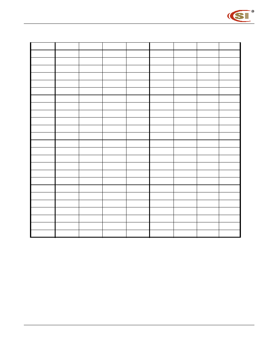
Table 17. Pull down and pull up current values
Temperature (Tambient)
Typical
25�C
Minimum
70�C
Maximum
0�C
Vdd/Vddq
Typical
2.5V
Minimum
2.3V
Maximum
2.7V
0.2
12.2
13.5
9.2
18.2
-12.2
-14.5
-9.2
-20.0
0.3
18.1
20.1
13.8
26.0
-18.1
-21.2
-13.8
-29.8
0.4
24.1
26.6
18.4
33.9
-24.0
-27.7
-18.4
-38.8
0.5
29.8
33.0
23.0
41.8
-29.8
-34.1
-23.0
-46.8
0.6
34.6
39.1
27.7
49.4
-34.3
-40.5
-27.7
-54.4
0.7
39.4
44.2
32.2
56.8
-38.1
-46.9
-32.2
-61.8
0.8
43.7
49.8
36.8
63.2
-41.1
-53.1
-36.0
-69.5
0.9
47.5
55.2
39.6
69.9
-41.8
-59.4
-38.2
-77.3
1.0
51.3
60.3
42.6
76.3
-46.0
-65.5
-38.7
-85.2
1.1
54.1
65.2
44.8
82.5
-47.8
-71.6
-39.0
-93.0
1.2
56.2
69.9
46.2
88.3
-49.2
-77.6
-39.2
-100.6
1.3
57.9
74.2
47.1
93.8
-50.0
-83.6
-39.4
-108.1
1.4
59.3
78.4
47.4
99.1
-50.5
-89.7
-39.6
-115.5
1.5
60.1
82.3
47.7
103.8
-50.7
-95.5
-39.9
-123.0
1.6
60.5
85.9
48.0
108.4
-51.0
-101.3
-40.1
-130.4
1.7
61.0
89.1
48.4
112.1
-51.1
-107.1
-40.2
-136.7
1.8
61.5
92.2
48.9
115.9
-51.3
-112.4
-40.3
-144.2
1.9
62.0
95.3
49.1
119.6
-51.5
-118.7
-40.4
-150.5
2.0
62.5
97.2
49.4
123.3
-51.6
-124.0
-40.5
-156.9
2.1
62.9
99.1
49.6
126.5
-51.8
-129.3
-40.6
-163.2
2.2
63.3
100.9
49.8
129.5
-52.0
-134.6
-40.7
-169.6
2.3
63.8
101.9
49.9
132.4
-52.2
-139.9
-40.8
-176.0
2.4
64.1
102.8
50.0
135.0
-52.3
-145.2
-40.9
-181.3
2.5
64.6
103.8
50.2
137.3
-52.5
-150.5
-41.0
-187.6
2.6
64.8
104.6
50.4
139.2
-52.7
-155.3
-41.1
-192.9
2.7
65.0
105.4
50.5
140.8
-52.8
-160.1
-41.2
-198.2
IC4
3R16160
Integrated Circuit Solution Inc.
41
DDR001-0B
11
/
10
/
2004
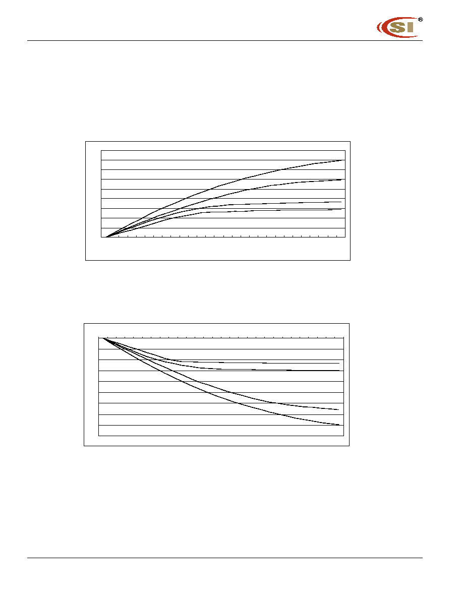
The above characteristics are specified under best, worst and normal process variation/conditions
Half strength driver
1. The nominal pulldown V-I curve for DDR SDRAM devices will be within the inner bounding lines of the V-I curve of Figure a.
2. The full variation in driver pulldown current from minimum to maximum process, temperature and voltage will lie within the outer
bounding lines the of the V-I curve of Figure a.
3. Thenominal pullup V-I curve for DDR SDRAM devices will be within the inner bounding lines of the V-I curve of below Figure b.
4. The Full variation in driver pullup current from minimum to maximum process, temperature and voltage will lie within the outer
bounding lines of the V-I curve of Figure b.
5. The full variation in the ratio of the maximum to minimum pullup and pulldown current will not exceed 1.7, for device drain to source
voltage from 0 to VDDQ/2
6. The Full variation in the ratio of the nominal pullup to pulldown current should be unity �10%, for device drain to source voltages
from 0 to VDDQ/2
Figure 26. I/V characteristics for input/output buffers:Pull up(above) and pull down(below)
I
out
(
m
A
)
Minimum
Typical Low
Typical High
Maximum
0
10
20
30
40
50
60
70
80
90
0.0
1.0
2.0
Iout
(
m
A)
Vout(V)
Maximum
Typical High
Minumum
I
out(
m
A)
- 9 0
- 8 0
- 7 0
- 6 0
- 5 0
- 4 0
- 3 0
- 2 0
- 1 0
0
0.0
0.5
1.0
1.5
2.0
2.5
Typical Low
V
DDQ
--
Vout(V)
IC4
3R16160
4
2 Integrated Circuit Solution Inc.
DDR001
-
0B
11
/
10
/
2004
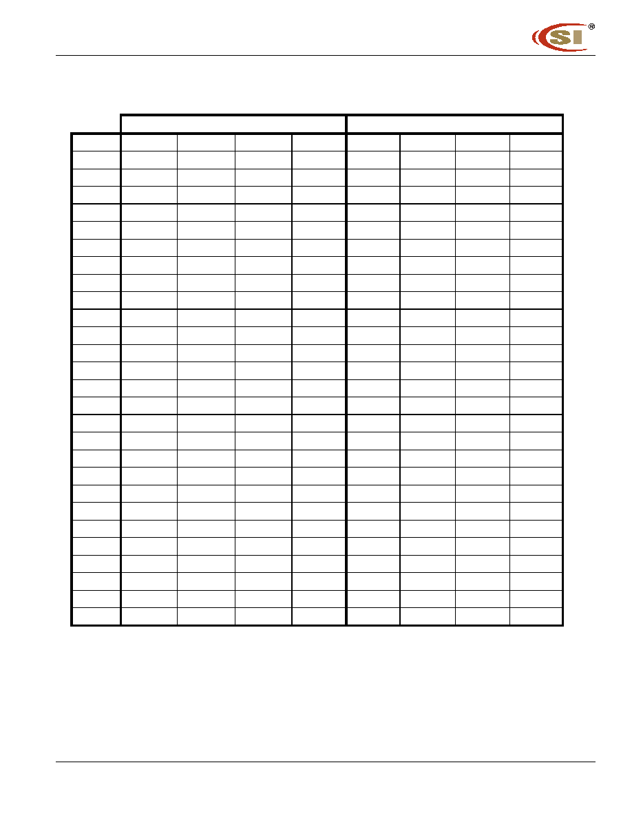
Table 18. Pull down and pull up current values
Temperature (Tambient)
Typical 25�C
Minimum 70�C
Maximum 0�C
Vdd/Vddq
Typical 2.5V
Minimum 2.3V
Maximum 2.7V
Pulldown Current (mA)
Pullup Current (mA)
Voltage (V)
Typical Low
Typical High
Minimum
Maximum
Typical Low
Typical High
Minimum
Maximum
0.1
3.4
3.8
2.6
5.0
-3.5
-4.3
-2.6
-5.0
0.2
6.9
7.6
5.2
9.9
-6.9
-8.2
-5.2
-9.9
0.3
10.3
11.4
7.8
14.6
-10.3
-12.0
-7.8
-14.6
0.4
13.6
15.1
10.4
19.2
-13.6
-15.7
-10.4
-19.2
0.5
16.9
18.7
13.0
23.6
-16.9
-19.3
-13.0
-23.6
0.6
19.6
22.1
15.7
28.0
-19.4
-22.9
-15.7
-28.0
0.7
22.3
25.0 18.2
32.2
-21.5
-26.5
-18.2
-32.2
0.8
24.7
28.2
20.8
35.8
-23.3
-30.1
-20.4
-35.8
0.9
26.9
31.3
22.4
39.5
-24.8
-33.6
-21.6
-39.5
1.0
29.0
34.1
24.1
43.2
-26.0
-37.1
-21.9
-43.2
1.1
30.6
36.9
25.4
46.7
-27.1
-40.3
-22.1
-46.7
1.2
31.8
39.5
26.2
50.0
-27.8
-43.1
-22.2
-50.0
1.3
32.8
42.0
26.6
53.1
-28.3
-45.8
-22.3
-53.1
1.4
33.5
44.4
26.8
56.1
-28.6
-48.4
-22.4
-56.1
1.5
34.0
46.6
27.0
58.7
-28.7
-50.7
-22.6
-58.7
1.6
34.3
48.6
27.2
61.4
-28.9
-52.9
-22.7
-61.4
1.7
34.5
50.5
27.4
63.5
-28.9
-55.0
-22.7
-63.5
1.8
34.8
52.2
27.7
65.6
-29.0
-56.8
-22.8
-65.6
1.9
35.1
53.9
27.8
67.7
-29.2
-58.7
-22.9
-67.7
2.0
35.4
55.0
28.0
69.8
-29.2
-60.0
-22.9
-69.8
2.1
35.6
56.1
28.1
71.6
-29.3
-61.2
-23.0
-71.6
2.2
35.8
57.1
28.2
73.3
-29.5
-62.4
-23.0
-73.3
2.3
36.1
57.7
28.3
74.9
-29.5
-63.1
-23.1
-74.9
2.4
36.3
58.2
28.3
76.4
-29.6
-63.8
-23.2
-76.4
2.5
36.5
58.7
28.4
77.7
-29.7
-64.4
-23.2
-77.7
2.6
36.7
59.2
28.5
78.8
-29.8
-65.1
-23.3
-78.8
2.7
36.8
59.6
28.6
79.7
-29.9
-65.8
-23.3
-79.7
IC4
3R16160
Integrated Circuit Solution Inc.
43
DDR001-0B
11
/
10
/
2004
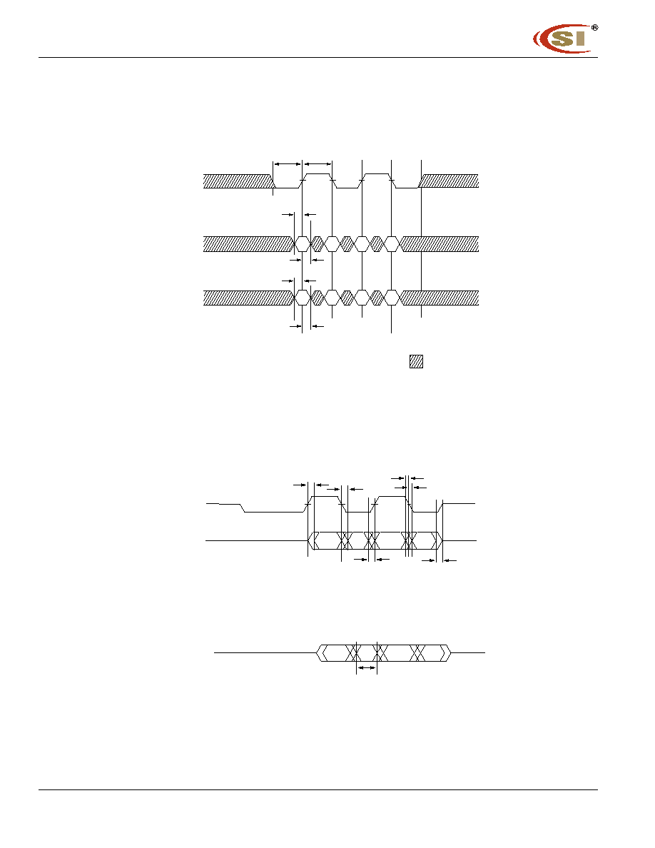
The above characteristics are specified under best, worst and normal process variation/conditions
Figure 36 - DATA INPUT (WRITE) TIMING
DI
n
= Data In for column
n
Burst Length = 4 in the case shown
3 subsequent elements of Data In are applied in the programmed
order following DI
n
Figure 37 - DATA OUTPUT (READ) TIMING
1. tDQSQ max occurs when DQS is the earliest among DQS and DQ signals to transition.
2. tDQSQ min occurs when DQS is the latest among DQS and DQ signals to transition.
3. tDQSQ nom, shown for reference, occurs when DQS transitions in the center among DQ signal transitions.
DON'T CARE
DQ
DM
DQS
DI
n
tDS
tDH
tDS
tDH
tDSL tDSH
t
min
DQSQ
t
max
DQSQ
DQ
DQS
t
min
DQSQ
t
max
DQSQ
t
nom
DQSQ
Burst Length = 4 in the case shown
tDV
DQS, DQ
IC4
3R16160
4
4 Integrated Circuit Solution Inc.
DDR001
-
0B
11
/
10
/
2004
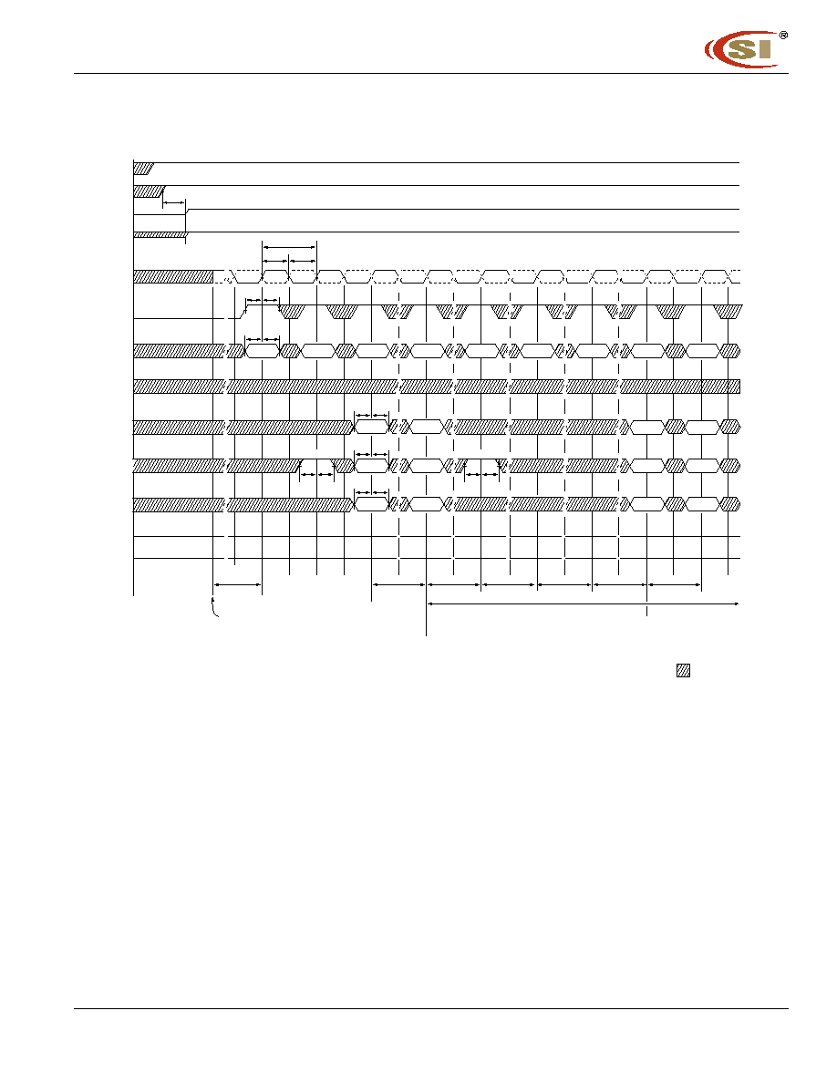
Figure 38 - INITIALIZE AND MODE REGISTER SETS
CKE
LVCMOS LOW LEVEL
DQ
BA0, BA1
200 cycles of CLK**
Extended
Mode
Register
Set
Load
Mode
Register,
Reset DLL
(with A8 = H)
Load
Mode
Register
(with A8 = L)
tMRD
tMRD
tMRD
tRP
tRFC
tRFC
t IS
Power-up:
VDD and
CLK stable
T = 200
�
s
(
)
(
)
(
)
(
)
(
)
(
)
(
)
(
)
High-Z
tIH
(
)
(
)
(
)
(
)
(
)
(
)
(
)
(
)
(
)
(
)
(
)
(
)
(
)
(
)
(
)
(
)
(
)
(
)
(
)
(
)
DM
(
)
(
)
(
)
(
)
(
)
(
)
(
)
(
)
(
)
(
)
(
)
(
)
(
)
(
)
(
)
(
)
(
)
(
)
(
)
(
)
(
)
(
)
(
)
(
)
(
)
(
)
DQS
High-Z
(
)
(
)
(
)
(
)
(
)
(
)
(
)
(
)
(
)
(
)
(
)
(
)
(
)
(
)
(
)
(
)
(
)
(
)
(
)
(
)
A0-A9, A11
(
)
(
)
(
)
(
)
(
)
(
)
(
)
(
)
A10
ALL BANKS
DON'T CARE
CK
/CK
tCK
tCH
tCL
VTT
(system*)
t VTD
VREF
VDD
VDDQ
COMMAND
MRS
NOP
PRE
EMRS
AR
(
)
(
)
(
)
(
)
(
)
(
)
(
)
(
)
(
)
(
)
(
)
(
)
(
)
(
)
(
)
(
)
AR
tIS tIH
BA0=H,
BA1=L
tIS tIH
tIS tIH
BA0=L,
BA1=L
tIS tIH
(
)
(
)
(
)
(
)
(
)
(
)
(
)
(
)
(
)
(
)
(
)
(
)
(
)
(
)
(
)
(
)
(
)
(
)
(
)
(
)
(
)
(
)
(
)
(
)
(
)
(
)
(
)
(
)
(
)
(
)
(
)
(
)
(
)
(
)
(
)
(
)
(
)
(
)
(
)
(
)
(
)
(
)
(
)
(
)
(
)
(
)
(
)
(
)
(
)
(
)
(
)
(
)
(
)
(
)
(
)
(
)
(
)
(
)
(
)
(
)
(
)
(
)
(
)
(
)
(
)
(
)
(
)
(
)
(
)
(
)
(
)
(
)
(
)
(
)
(
)
(
)
(
)
(
)
(
)
(
)
CODE
tIS tIH
CODE
MRS
BA0=L,
BA1=L
CODE
CODE
(
)
(
)
(
)
(
)
(
)
(
)
(
)
(
)
PRE
ALL BANKS
tIS tIH
RA
RA
ACT
BA
* = VTT is not applied directly to the device, however tVTD must be greater than or equal to zero to avoid device latch-up.
** = tMRD is required before any command can be applied, and 200 cycles of CK are required before a READ command can be applied.
The two Auto Refresh commands may be moved to follow the first MRS, but precede the second PRECHARGE ALL command.
(
)
(
)
(
)
(
)
CODE
CODE
IC4
3R16160
Integrated Circuit Solution Inc.
45
DDR001-0B
11
/
10
/
2004
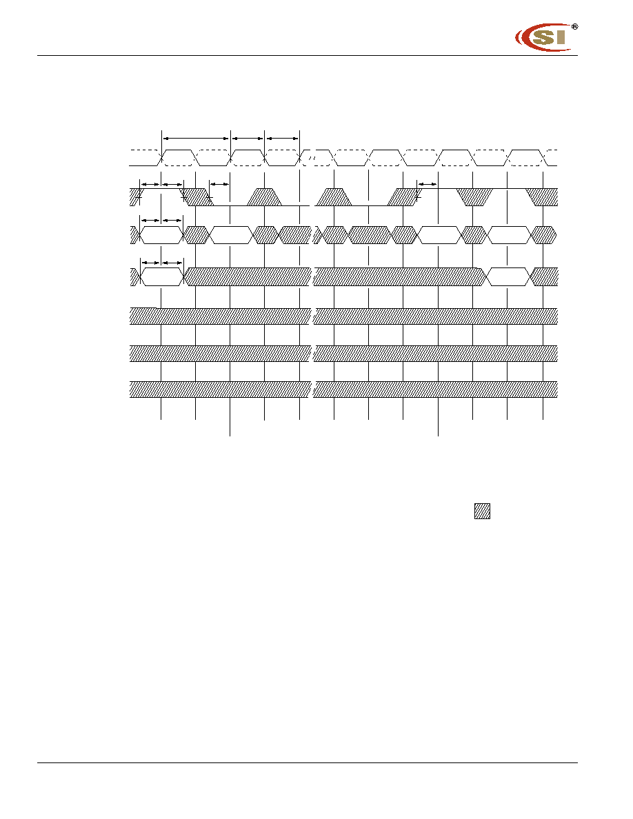
Figure 39 - POWER-DOWN MODE
CK
/CK
COMMAND
VALID*
NOP
ADDR
CKE
VALID
VALID
DON'T CARE
No column accesses are allowed to be in progress at the time Power-Down is entered
* = If this command is a PRECHARGE (or if the device is already in the idle state) then the Power-Down
mode shown is Precharge Power Down. If this command is an ACTIVE (or if at least one row is already
active) then the Power-Down mode shown is Active Power Down.
DQ
DM
DQS
VALID
tCK
tCH
tCL
tIS
tIS
tIH
tIS
tIS tIH
tIH
tIS
Enter
Power-Down
Mode
Exit
Power-Down
Mode
(
)
(
)
(
)
(
)
(
)
(
)
(
)
(
)
(
)
(
)
(
)
(
)
(
)
(
)
(
)
(
)
(
)
(
)
(
)
(
)
(
)
(
)
(
)
(
)
(
)
(
)
NOP
IC4
3R16160
4
6 Integrated Circuit Solution Inc.
DDR001
-
0B
11
/
10
/
2004
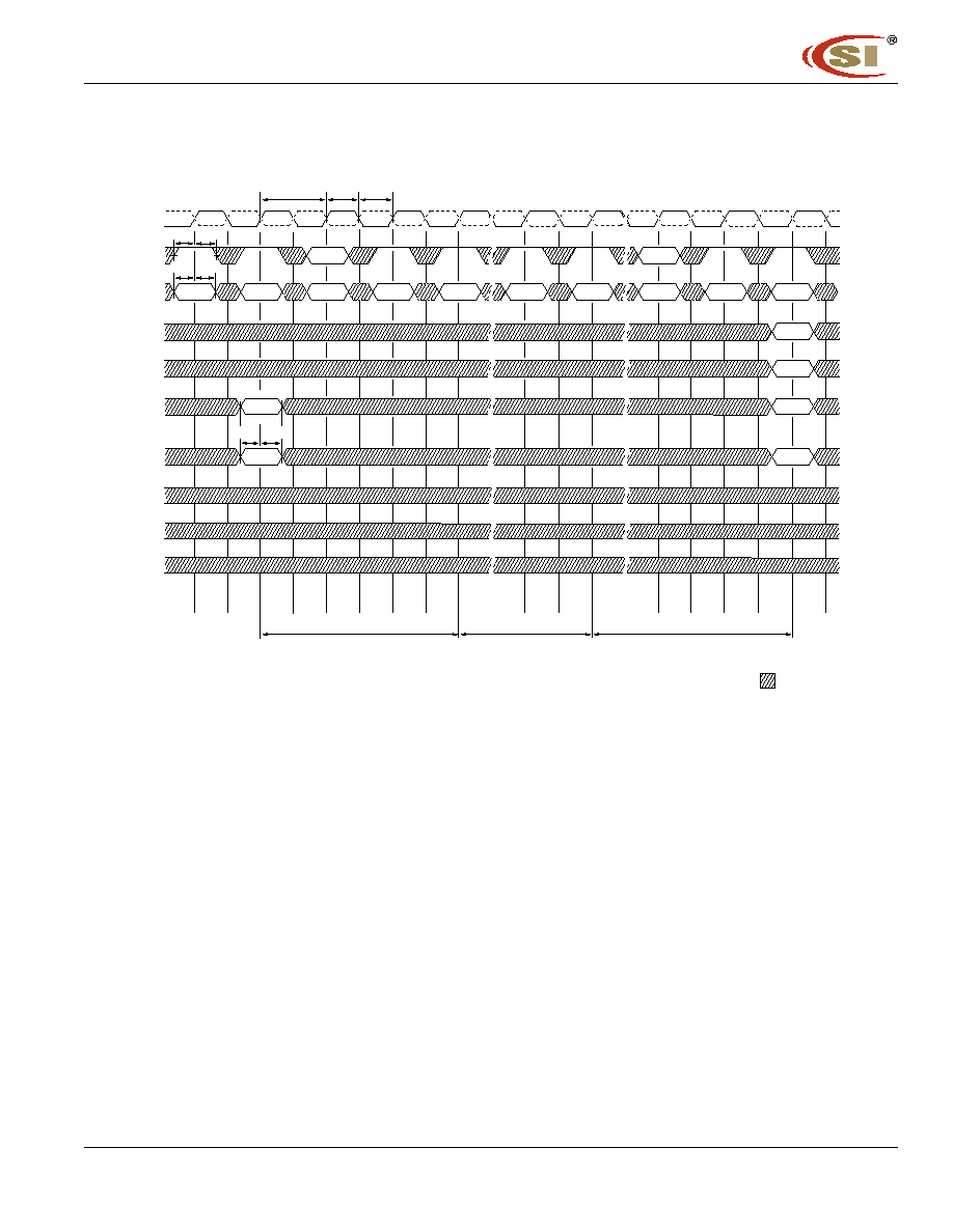
Figure 40 - AUTO REFRESH MODE
CK
/CK
COMMAND
NOP
VALID
VALID
NOP
NOP
PRE
A0-A8
CKE
RA
RA
A9, A11
A10
BA0, BA1
*Bank(s)
BA
DON'T CARE
* = "Don't Care", if A10 is HIGH at this point; A10 must be HIGH if more than one bank is active (i.e. must precharge all active banks)
PRE = PRECHARGE, ACT = ACTIVE, RA = Row Address, BA = Bank Address, AR = AUTOREFRESH
NOP commands are shown for ease of illustration; other valid commands may be possible at these times
DM, DQ and DQS signals are all "Don't Care"/High-Z for operations shown
AR
NOP
AR
NOP
ACT
NOP
ONE BANK
ALL BANKS
tCK
tCH
tCL
tIS
tIS
tIH
tIH
tIS tIH
RA
(
)
(
)
(
)
(
)
(
)
(
)
(
)
(
)
(
)
(
)
(
)
(
)
(
)
(
)
(
)
(
)
(
)
(
)
(
)
(
)
(
)
(
)
(
)
(
)
(
)
(
)
(
)
(
)
(
)
(
)
(
)
(
)
(
)
(
)
(
)
(
)
(
)
(
)
(
)
(
)
(
)
(
)
(
)
(
)
(
)
(
)
(
)
(
)
(
)
(
)
(
)
(
)
(
)
(
)
(
)
(
)
(
)
(
)
(
)
(
)
(
)
(
)
(
)
(
)
DQ
DM
DQS
(
)
(
)
(
)
(
)
(
)
(
)
(
)
(
)
(
)
(
)
(
)
(
)
(
)
(
)
(
)
(
)
(
)
(
)
(
)
(
)
(
)
(
)
(
)
(
)
t RC
t RP
t RC
IC4
3R16160
Integrated Circuit Solution Inc.
47
DDR001-0B
11
/
10
/
2004
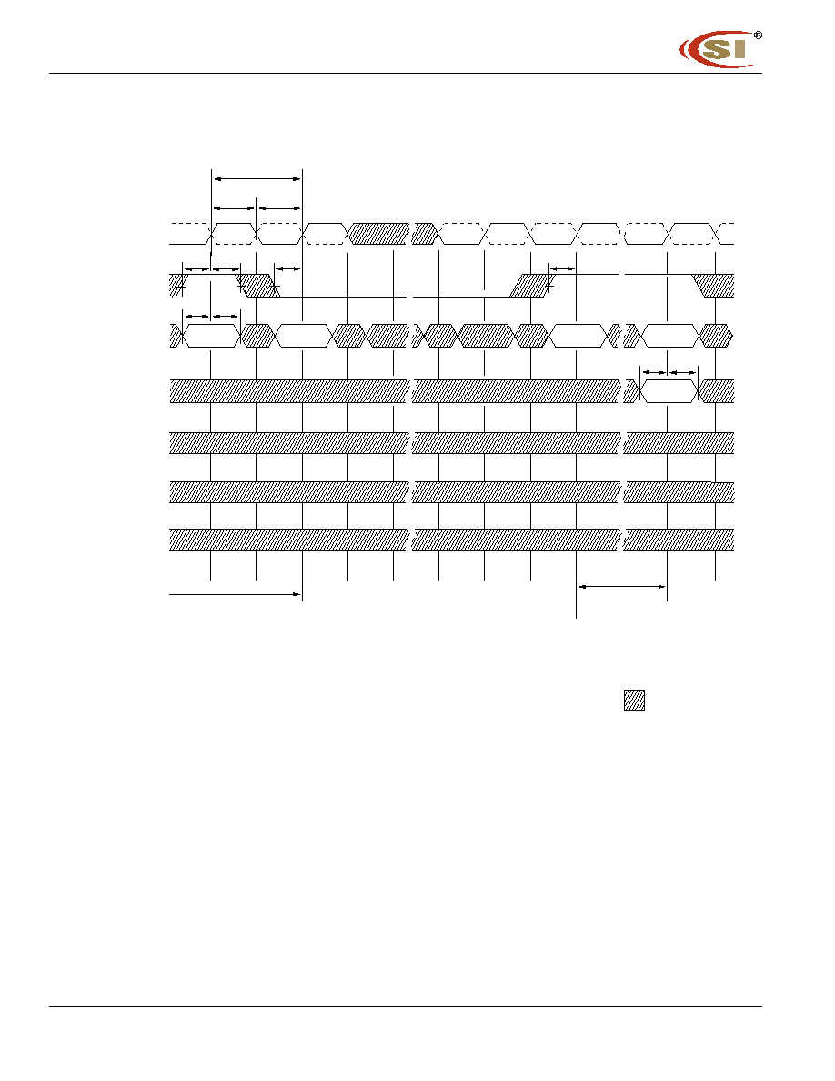
Figure 41 - SELF REFRESH MODE
CK
/CK
COMMAND
NOP
AR
ADDR
CKE
VALID
DON'T CARE
DQ
DM
DQS
VALID
NOP
tCK
clock must be stable before
exiting Self Refresh mode
tRP*
tCH
tCL
tIS
tIS
tIH
tIS
tIS tIH
tIH
tIS
Enter
Self Refresh
Mode
Exit
Self Refresh
Mode
(
)
(
)
(
)
(
)
(
)
(
)
(
)
(
)
(
)
(
)
(
)
(
)
(
)
(
)
(
)
(
)
(
)
(
)
(
)
(
)
(
)
(
)
(
)
(
)
(
)
(
)
(
)
(
)
(
)
(
)
(
)
(
)
(
)
(
)
(
)
(
)
(
)
(
)
(
)
(
)
(
)
(
)
(
)
(
)
(
)
(
)
(
)
(
)
(
)
(
)
(
)
(
)
* = Device must be in the "All banks idle" state prior to entering Self Refresh mode
** = tXSNR is required before any non-READ command can be applied, and tXSRD (200 cycles of CLK)
are required before a READ command can be applied.
tXSNR/
tXSRD**
IC4
3R16160
48 Integrated Circuit Solution Inc.
DDR001
-
0B
11
/
10
/
2004
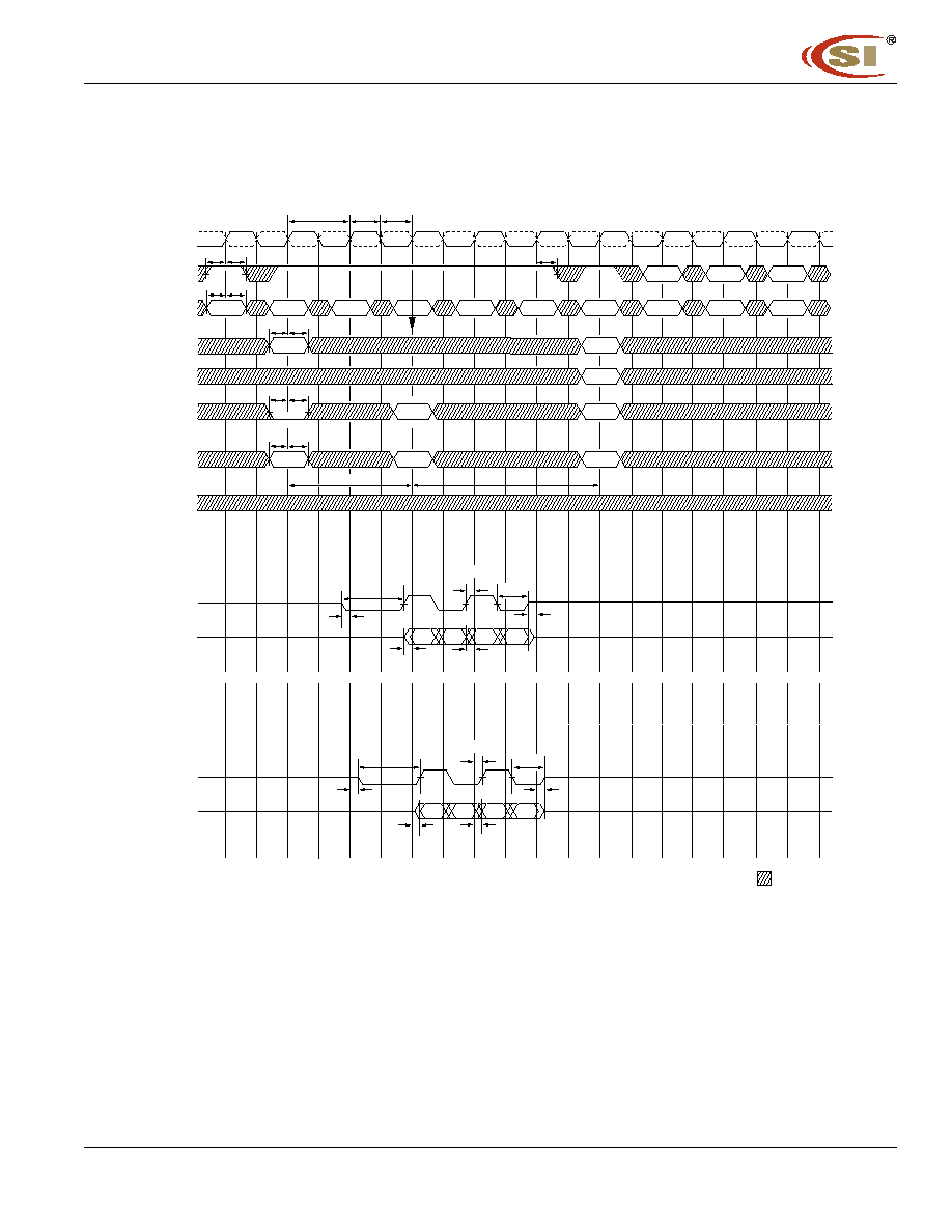
Figure 42 - READ - WITHOUT AUTO PRECHARGE
CK
/CK
COMMAND
NOP
NOP
PRE
READ
CKE
Col
n
RA
RA
A10
BA0, BA1
Bank
x
*Bank
x
DON'T CARE
DO
n
= Data Out from column
n
Burst Length = 4 in the case shown
3 subsequent elements of Data Out are provided in the programmed order following DO
n
DIS AP = Disable Autoprecharge
* = "Don't Care", if A10 is HIGH at this point
PRE = PRECHARGE, ACT = ACTIVE, RA = Row Address, BA = Bank Address
NOP commands are shown for ease of illustration; other commands may be valid at these times
DQ
DM
DQS
Case 1:
tAC/tDQSCK = min
DQ
DQS
NOP
NOP
ACT
NOP
NOP
NOP
VALID
VALID
VALID
DIS AP
ONE BANK
ALL BANKS
tCK
tCH
tCL
tIS
tIS
tIH
tIH
tIS
tIS
tIH
tIH
tIH
tIS tIH
tRPRE
tRPRE
tRP
t
t
RA
CL = 2
t
min
HZ
t
max
HZ
t
min
LZ
t
max
LZ
t
max
LZ
t
min
AC
t
max
t
min
t
max
AC
Bank
x
x4:A0-A9
x8:A0-A8
x16:A0-A7
x4:A11
x8:A9, A11
x16:A8, A9, A11
DO
n
DO
n
DQSCK
RPST
DQSCK
RPST
t
min
LZ
Start Autoprecharge
IC4
3R16160
Case 2:
tAC/tDQSCK = max
Integrated Circuit Solution Inc.
49
DDR001-0B
11
/
10
/
2004
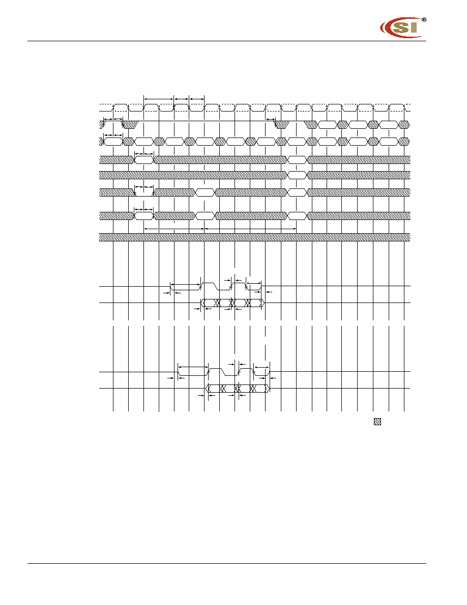
Figure 43 - READ - WITH AUTO PRECHARGE
CK
/CK
COMMAND
NOP
NOP
PRE
READ
CKE
Col
n
RA
RA
A10
BA0, BA1
Bank
x
*Bank
x
DON'T CARE
DO
n
= Data Out from column
n
Burst Length = 4 in the case shown
3 subsequent elements of Data Out are provided in the programmed order following DO
n
DIS AP = Disable Autoprecharge
* = "Don't Care", if A10 is HIGH at this point
PRE = PRECHARGE, ACT = ACTIVE, RA = Row Address, BA = Bank Address
NOP commands are shown for ease of illustration; other commands may be valid at these times
DQ
DM
DQS
DQ
DQS
NOP
NOP
ACT
NOP
NOP
NOP
VALID
VALID
VALID
DIS AP
ONE BANK
ALL BANKS
tCK
tCH
tCL
tIS
tIS
tIH
tIH
tIS
tIS
tIH
tIH
tIH
tIS tIH
tRPRE
tRPRE
tRP
t
t
RA
CL = 2
t
min
HZ
t
max
HZ
t
min
LZ
t
max
LZ
t
max
LZ
t
min
AC
t
max
t
min
t
max
AC
Bank
x
x4:A0-A9
x8:A0-A8
x16:A0-A7
x4:A11
x8:A9, A11
x16:A8, A9, A11
DO
n
DO
n
DQSCK
RPST
DQSCK
RPST
t
min
LZ
Case 1:
tAC/tDQSCK = min
Case 2:
tAC/tDQSCK = max
IC4
3R16160
50 Integrated Circuit Solution Inc.
DDR001
-
0B
11
/
10
/
2004
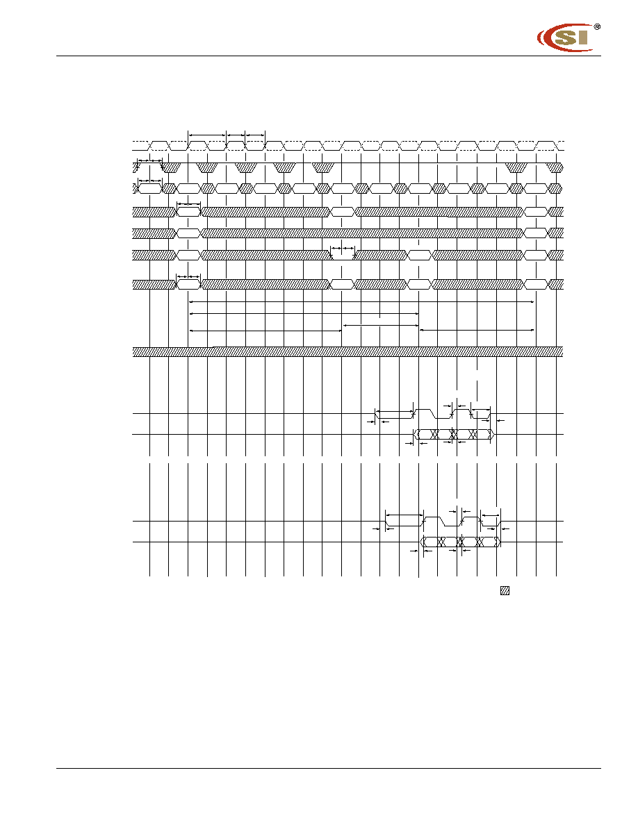
Figure 44 - BANK READ ACCESS
CK
/CK
COMMAND
NOP
NOP
NOP
NOP
READ
ACT
CKE
RA
RA
RA
RA
RA
A10
BA0, BA1
Bank
x
Bank
x
NOP
NOP
NOP
PRE
DIS AP
ONE BANK
ALL BANKS
tCK
tCH
tCL
tIS
tIS
tIH
tIS
tIS
tIH
tIH
tIH
tIS tIH
RA
DO
n = Data Out from column n
Burst Length = 4 in the case shown
3 subsequent elements of Data Out are provided in the programmed order following DO
n
DIS AP = Disable Autoprecharge
* = "Don't Care", if A10 is HIGH at this point
PRE = PRECHARGE, ACT = ACTIVE, RA = Row Address, BA = Bank Address
NOP commands are shown for ease of illustration; other commands may be valid at these times
Note that tRCD > tRCD MIN so that the same timing applies if Autoprecharge is enabled (in which case tRAS would be limiting)
tRCD
tRAS
tRC
*Bank
x
Bank
x
tRP
CL = 2
Col
n
ACT
x4:A0-A9
x8:A0-A8
x16:A0-A7
x4:A11
x8:A9, A11
x16:A8, A9, A11
DON'T CARE
DQ
DM
DQS
Case 1:
tAC/tDQSCK = min
DQ
DQS
tRPRE
tRPRE
t
t
t
min
HZ
t
max
HZ
t
min
LZ
t
max
LZ
t
max
LZ
t
min
LZ
t
min
AC
t
max
t
min
t
max
AC
DO
n
DO
n
DQSCK
RPST
DQSCK
RPST
IC4
3R16160
Case 2:
tAC/tDQSCK = max
Integrated Circuit Solution Inc.
51
DDR001-0B
11
/
10
/
2004
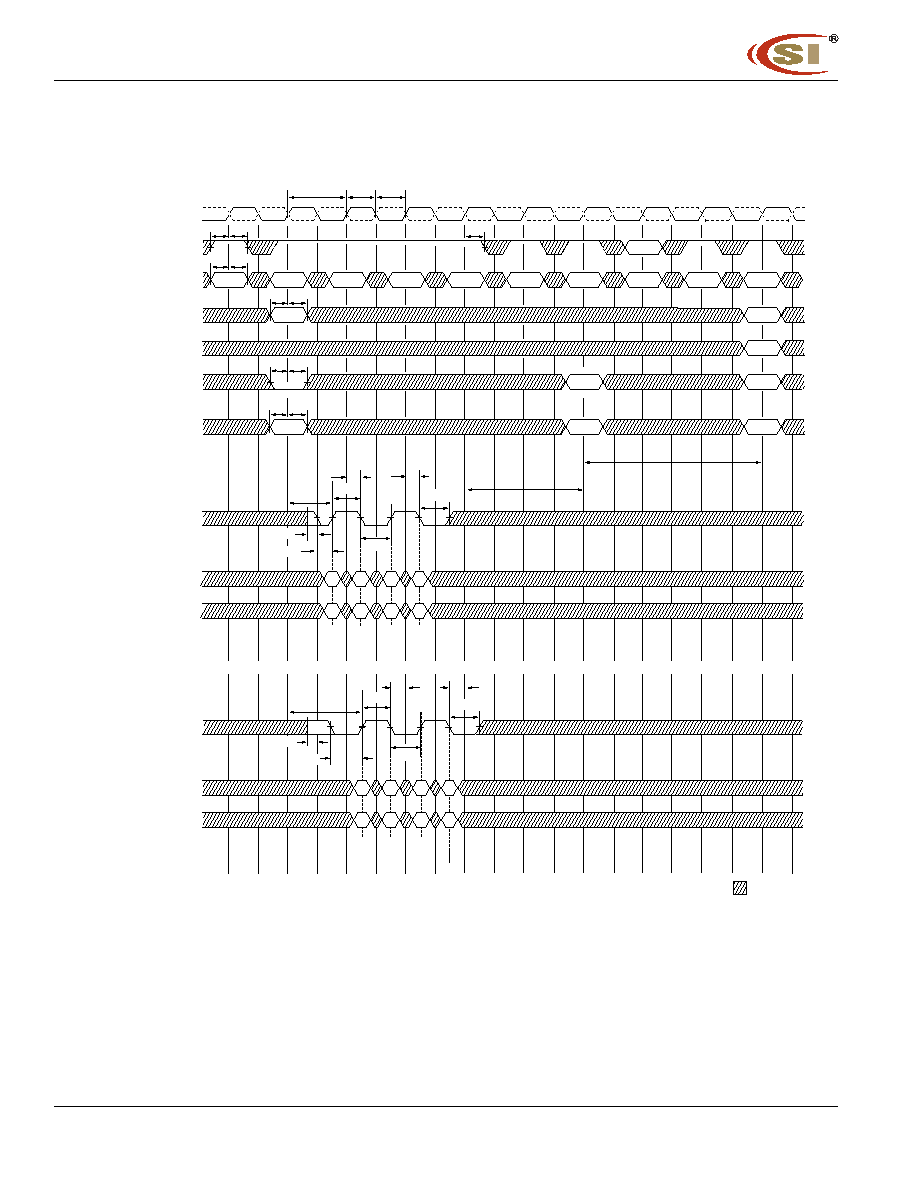
Figure 45 - WRITE - WITHOUT AUTO PRECHARGE
CK
/CK
COMMAND
NOP
NOP
NOP
WRITE
CKE
Col
n
RA
RA
A10
BA0, BA1
Bank
x
*Bank
x
BA
DON'T CARE
DI
n
= Data In for column
n
Burst Length = 4 in the case shown
3 subsequent elements of Data In are applied in the programmed order following DI
n
DIS AP = Disable Autoprecharge
* = "Don't Care", if A10 is HIGH at this point
PRE = PRECHARGE, ACT = ACTIVE, RA = Row Address, BA = Bank Address
NOP commands are shown for ease of illustration; other valid commands may be possible at these times
NOP
NOP
PRE
NOP
VALID
ACT
NOP
DIS AP
ONE BANK
ALL BANKS
tCK
tCH
tCL
tIS
tIS
tIH
tIH
tIS
tIS
tIH
tIH
tRP
tIH
tIS tIH
RA
x4:A0-A9
x8:A0-A8
x16:A0-A7
x4:A11
x8:A9, A11
x16:A8, A9, A11
DQ
DM
DQS
DI
n
t
tDQSS
t
t
Case 1:
tDQSS = min
Case 2:
tDQSS = max
DQ
DM
DQS
DI
n
t
tWR
tDQSS
t
t
t
t
WPST
DQSH
DQSL
tWPRES
WPST
DQSH
DQSL
WPRE
WPRES
tWPRE
tDSS
tDSS
tDSH
tDSH
IC4
3R16160
52 Integrated Circuit Solution Inc.
DDR001
-
0B
11
/
10
/
2004
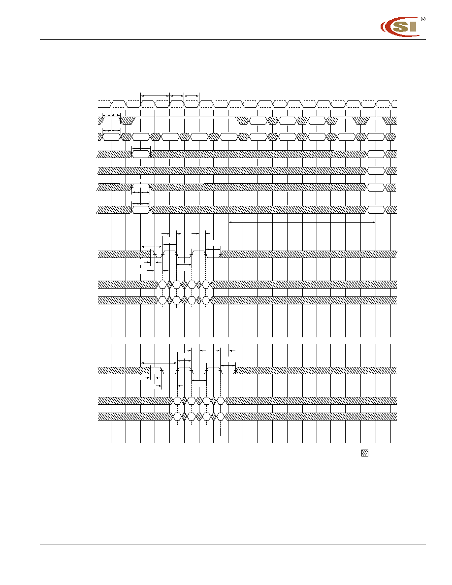
Figure 46 - WRITE - WITH AUTO PRECHARGE
CK
/CK
COMMAND
NOP
NOP
NOP
WRITE
CKE
Col
n
RA
RA
A10
BA0, BA1
Bank
x
BA
DON'T CARE
DI
n
= Data In for column
n
Burst Length = 4 in the case shown
3 subsequent elements of Data In are applied in the programmed order following DI
n
EN AP = Enable Autoprecharge
ACT = ACTIVE, RA = Row Address, BA = Bank Address
NOP commands are shown for ease of illustration; other valid commands may be possible at these times
NOP
NOP
NOP
NOP
VALID
VALID
ACT
NOP
EN AP
tCK
tCH
tCL
tIS
tIS
tIH
tIS
tIS
tIH
tIH
tDAL
RA
VALID
tIH
x4:A0-A9
x8:A0-A8
x16:A0-A7
x4:A11
x8:A9, A11
x16:A8, A9, A11
DQ
DM
DQS
DI
n
t
tDQSS
t
t
Case 1:
tDQSS = min
Case 2:
tDQSS = max
DQ
DM
DQS
DI
n
t
tDQSS
t
t
t
t
WPST
DQSH
DQSL
tWPRES
WPST
DQSH
DQSL
WPRE
WPRES
tWPRE
tDSS
tDSS
tDSH
tDSH
IC4
3R16160
Integrated Circuit Solution Inc.
53
DDR001-0B
11
/
10
/
2004
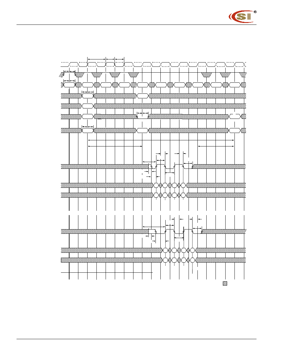
Figure 47 - BANK WRITE ACCESS
CK
/CK
COMMAND
NOP
NOP
NOP
WRITE
ACT
CKE
RA
A10
BA0, BA1
Bank
x
Bank
x
DON'T CARE
DI
n
= Data In for column
n
Burst Length = 4 in the case shown
3 subsequent elements of Data In are applied in the programmed order following DI
n
DIS AP = Disable Autoprecharge
* = "Don't Care", if A10 is HIGH at this point
PRE = PRECHARGE, ACT = ACTIVE, RA = Row Address
NOP commands are shown for ease of illustration; other valid commands may be possible at these times
NOP
NOP
NOP
NOP
PRE
DIS AP
ONE BANK
ALL BANKS
tCK
tCH
tCL
tIS
tIS
tIH
tIS
tIS
tIH
tIH
tRCD
tRAS
tIH
tIS tIH
RA
x4:A0-A9
x8:A0-A8
x16:A0-A7
x4:A11
x8:A9, A11
x16:A8, A9, A11
Col
n
*Bank
x
RA
tWR
DQ
DM
DQS
DI
n
t
tDQSS
t
t
Case 1:
tDQSS = min
Case 2:
tDQSS = max
DQ
DM
DQS
DI
n
t
tDQSS
t
t
t
t
WPST
DQSH
DQSL
tWPRES
WPST
DQSH
DQSL
WPRE
WPRES
tWPRE
tDSS
tDSS
tDSH
tDSH
IC4
3R16160
54 Integrated Circuit Solution Inc.
DDR001
-
0B
11
/
10
/
2004
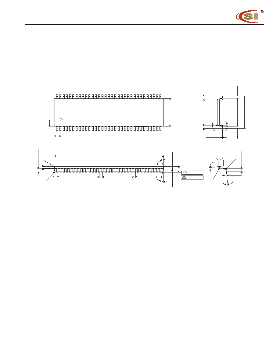
Package Diagram
66-Pin TSOP-II (400 mil)
Units : Millimeters
0.30
�
0.08
1.00
�
0.10
11.76
�
0.20
0.65TYP
(0.71)
22.22
�
0.10
0.125
(
0
.
80)
1
0
.1
6
0
.1
0
0 ~8
#1
#33
#66
#34
(1.50)
(1
.
5
0
)
0.65
�
0.08
1.
20
MA
X
(0
.
5
0
)
(0
.
5
0
)
(
10.
76
)
(10� )
(10
�
)
+0.075
-0.035
(0
.
8
0
)
0.10 MAX
0.075 MAX
[
]
0.
0
5
MI
N
(10� )
(10�)
(R0
.15
)
0.
21
0
0.
0
5
0.
66
5
0.
0
5
(R0.
15)
(4
�
)
(R
0
.2
5
)
(R0
.2
5)
0.
45
~
0
.
75
0.25TYP
NOTE
1. ( ) IS REFERENCE
IC4
3R16160
Integrated Circuit Solution Inc.
55
DDR001-0B
11
/
10
/
2004
Integrated Circuit Solution Inc.
HEADQUARTER:
NO.2, TECHNOLOGY RD. V, SCIENCE-BASED INDUSTRIAL PARK,
HSIN-CHU, TAIWAN, R.O.C.
TEL: 886-3-5780333
Fax: 886-3-5783000
BRANCH OFFICE:
7F, NO. 106, SEC. 1, HSIN-TAI 5
TH
ROAD,
HSICHIH TAIPEI COUNTY, TAIWAN, R.O.C.
TEL: 886-2-26962140
FAX: 886-2-26962252
http://www.icsi.com.tw
ORDERING INFORMATION (Pb-free Package)
Commercial Range: 0
C to 70
C
Frequency
Speed (ns)
Order Part No.
Package
200MHz
5
IC
43R16160-5T
400mil TSOP-2
200MHz
5
IC43R16160-5TG
400mil TSOP-2(Pb-free)
166MHz
6
IC43R16160-6T 400mil TSOP-2
166MHz
6
IC43R16160-6TG 400mil TSOP-2(Pb-free)
143MHz
7
IC43R16160-7T 400mil TSOP-2
143MHz
7
IC43R16160-7TG 400mil TSOP-2(Pb-free)
IC4
3R16160
56 Integrated Circuit Solution Inc.
DDR001
-
0B
11
/
10
/
2004