IC61C1024
IC61C1024L
Integrated Circuit Solution Inc.
1
AHSR008-0B 10/18/2001
Document Title
128K x 8 High-Speed SRAM
Revision History
Revision No
History
Draft Date
Remark
0A
Initial Draft
March 13,2001
0B
Revise typo on page 6 and page 8
October 18,2001
The attached datasheets are provided by ICSI. Integrated Circuit Solution Inc reserve the right to change the specifications and
products. ICSI will answer to your questions about device. If you have any questions, please contact the ICSI offices.
IC61C1024
IC61C1024L
2
Integrated Circuit Solution Inc.
AHSR008-0B 10/18/2001
128K x 8 HIGH-SPEED
CMOS STATIC RAM
ICSI reserves the right to make changes to its products at any time without notice in order to improve design and supply the best possible product. We assume no responsibility for any errors
which may appear in this publication. © Copyright 2000, Integrated Circuit Solution Inc.
DESCRIPTION
The
ICSI
IC61C1024 and IC61C1024L are very high-speed,
low power, 131,072-word by 8-bit CMOS static RAMs. They
are fabricated using
ICSI
's high-performance CMOS
technology. This highly reliable process coupled with innovative
circuit design techniques, yields higher performance and low
power consumption devices.
When
CE1
is HIGH or CE2 is LOW (deselected), the device
assumes a standby mode at which the power dissipation can
be reduced by using CMOS input levels.
Easy memory expansion is provided by using two Chip Enable
inputs,
CE1
and CE2. The active LOW Write Enable (
WE
)
controls both writing and reading of the memory.
The IC61C1024 and IC61C1024L are available in 32-pin
300mil SOJ, and 8*20mm TSOP-1, and 8*13.4mm TSOP-1
packages.
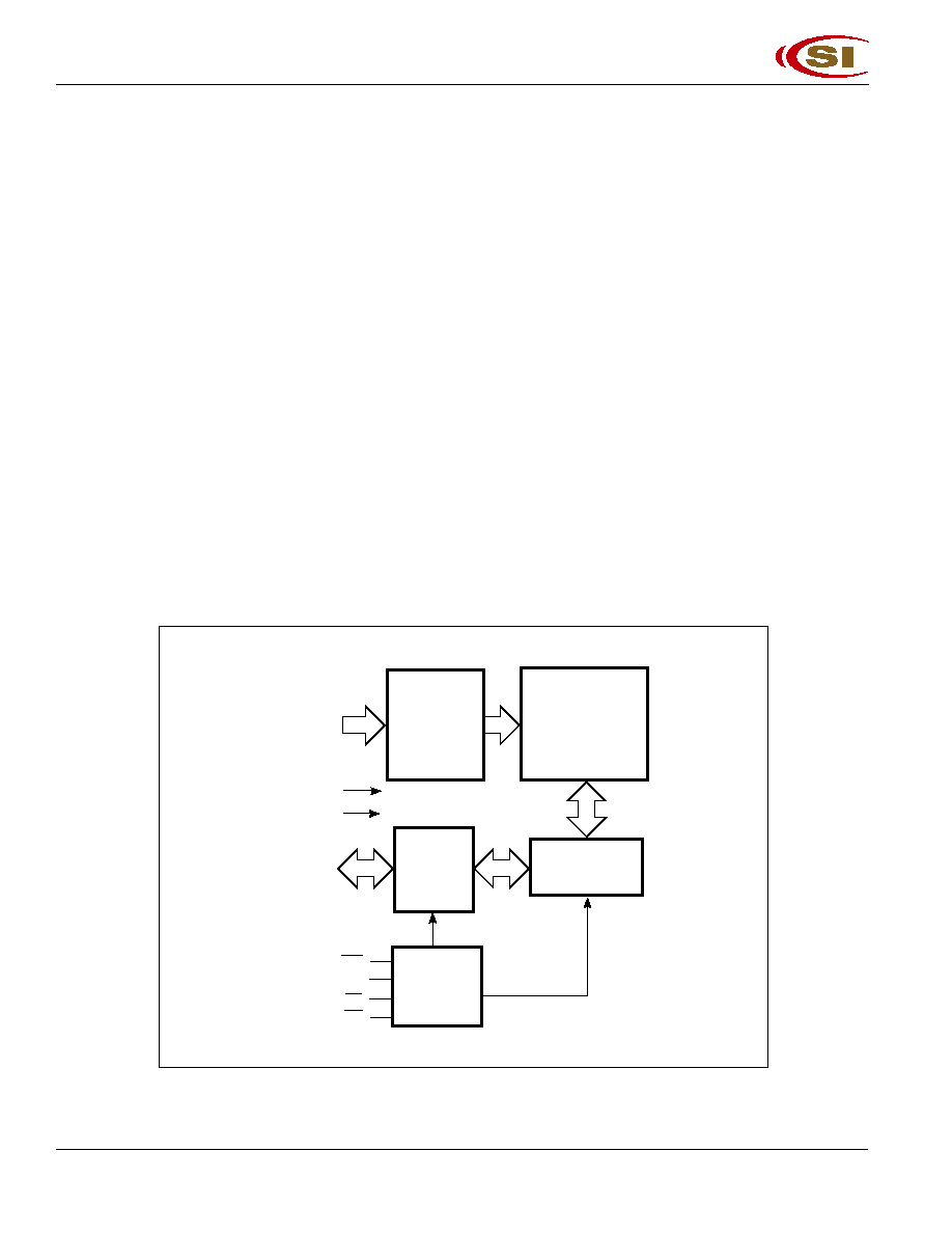
FUNCTIONAL BLOCK DIAGRAM
A0-A16
CE1
OE
WE
512 x 2048
MEMORY ARRAY
DECODER
COLUMN I/O
CONTROL
CIRCUIT
GND
VCC
I/O
DATA
CIRCUIT
I/O0-I/O7
CE2
FEATURES
∑ High-speed access time: 12, 15, 20, 25 ns
∑
Low active power: 600 mW (typical)
∑
Low standby power: 500 µW (typical) CMOS
standby
∑ Output Enable (
OE
) and two Chip Enable
(
CE1
and CE2) inputs for ease in applications
∑ Fully static operation: no clock or refresh
required
∑ TTL compatible inputs and outputs
∑ Single 5V (±10%) power supply
∑ Low power version available: IC61C1024L
∑ Commercial and industrial temperature ranges
available
IC61C1024
IC61C1024L
Integrated Circuit Solution Inc.
3
AHSR008-0B 10/18/2001
TRUTH TABLE
Mode
WE
WE
WE
WE
WE
CE1
CE1
CE1
CE1
CE1
CE2
OE
OE
OE
OE
OE
I/O Operation
Vcc Current
Not Selected
X
H
X
X
High-Z
I
SB
1
, I
SB
2
(Power-down)
X
X
L
X
High-Z
I
SB
1
, I
SB
2
Output Disabled H
L
H
H
High-Z
I
CC
1
, I
CC
2
Read
H
L
H
L
D
OUT
I
CC
1
, I
CC
2
Write
L
L
H
X
D
IN
I
CC
1
, I
CC
2
1
2
3
4
5
6
7
8
9
10
11
12
13
14
15
16
32
31
30
29
28
27
26
25
24
23
22
21
20
19
18
17
NC
A16
A14
A12
A7
A6
A5
A4
A3
A2
A1
A0
I/O0
I/O1
I/O2
GND
VCC
A15
CE2
WE
A13
A8
A9
A11
OE
A10
CE1
I/O7
I/O6
I/O5
I/O4
I/O3
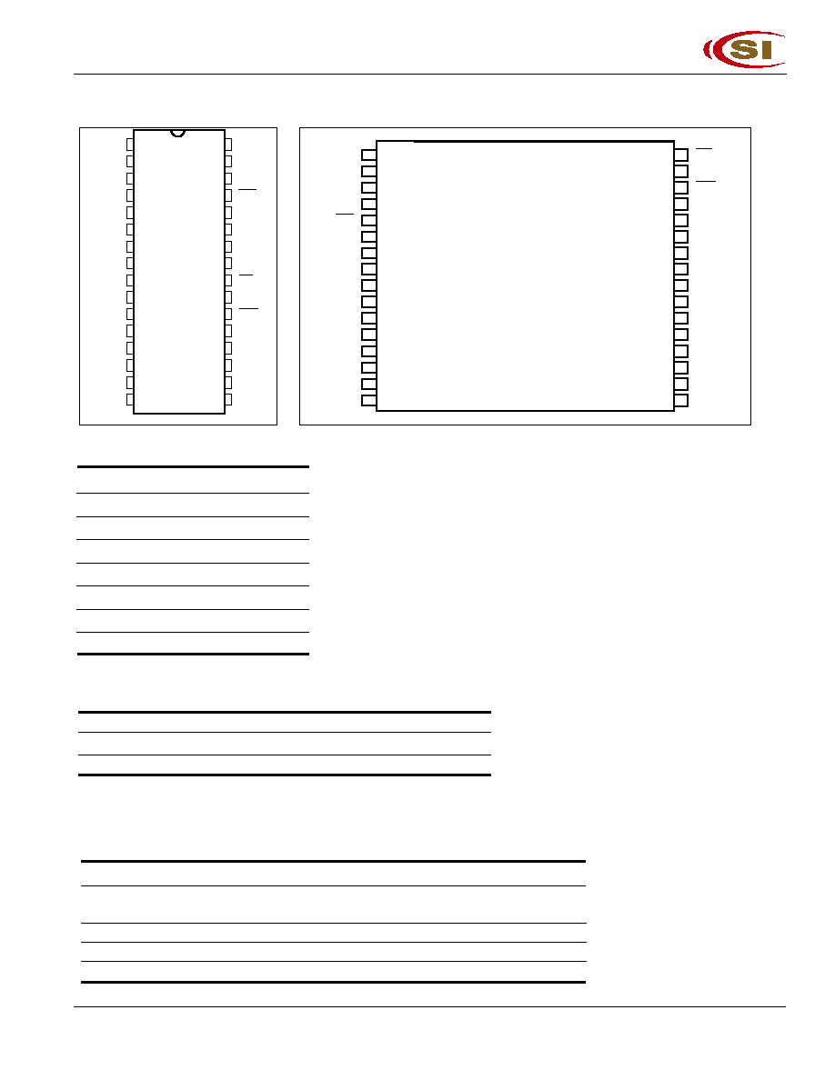
PIN CONFIGURATION
32-Pin SOJ
PIN DESCRIPTIONS
A0-A16
Address Inputs
CE1
Chip Enable 1 Input
CE2
Chip Enable 2 Input
OE
Output Enable Input
WE
Write Enable Input
I/O0-I/O7
Input/Output
Vcc
Power
GND
Ground
OPERATING RANGE
Range
Ambient Temperature
V
CC
Commercial
0∞C to +70∞C
5V ± 10%
Industrial
≠40∞C to +85∞C
5V ± 10%
1
2
3
4
5
6
7
8
9
10
11
12
13
14
15
16
32
31
30
29
28
27
26
25
24
23
22
21
20
19
18
17
A11
A9
A8
A13
WE
CE2
A15
VCC
NC
A16
A14
A12
A7
A6
A5
A4
OE
A10
CE1
I/O7
I/O6
I/O5
I/O4
I/O3
GND
I/O2
I/O1
I/O0
A0
A1
A2
A3
PIN CONFIGURATION
32-Pin 8x20mm TSOP-1 and 8x13.4mm TSOP-1
IC61C1024
IC61C1024L
4
Integrated Circuit Solution Inc.
AHSR008-0B 10/18/2001
ABSOLUTE MAXIMUM RATINGS
(1)
Symbol
Parameter
Value
Unit
V
TERM
Terminal Voltage with Respect to GND
≠0.5 to +7.0
V
T
BIAS
Temperature Under Bias
≠55 to +125
∞C
T
STG
Storage Temperature
≠65 to +150
∞C
P
T
Power Dissipation
1.5
W
I
OUT
DC Output Current (LOW)
20
mA
Notes:
1. Stress greater than those listed under ABSOLUTE MAXIMUM RATINGS may cause
permanent damage to the device. This is a stress rating only and functional operation
of the device at these or any other conditions above those indicated in the operational
sections of this specification is not implied. Exposure to absolute maximum rating
conditions for extended periods may affect reliability.
CAPACITANCE
(1,2)
Symbol
Parameter
Conditions
Max.
Unit
C
IN
Input Capacitance
V
IN
= 0V
5
pF
C
OUT
Output Capacitance
V
OUT
= 0V
7
pF
Notes:
1. Tested initially and after any design or process changes that may affect these parameters.
2. Test conditions: T
A
= 25∞C, f = 1 MHz, Vcc = 5.0V.
DC ELECTRICAL CHARACTERISTICS
(Over Operating Range)
Symbol Parameter
Test Conditions
Min.
Max.
Unit
V
OH
Output HIGH Voltage
V
CC
= Min., I
OH
= ≠4.0 mA
2.4
--
V
V
OL
Output LOW Voltage
V
CC
= Min., I
OL
= 8.0 mA
--
0.4
V
V
IH
Input HIGH Voltage
2.2
V
CC
+ 0.5
V
V
IL
Input LOW Voltage
(1)
≠0.3
0.8
V
I
LI
Input Leakage
GND
V
IN
V
CC
Com.
≠2
2
µA
Ind.
≠5
5
I
LO
Output Leakage
GND
V
OUT
V
CC
Com.
≠2
2
µA
Outputs Disabled
Ind.
≠5
5
Note:
1. V
IL
= ≠3.0V for pulse width less than 10 ns.
IC61C1024
IC61C1024L
Integrated Circuit Solution Inc.
5
AHSR008-0B 10/18/2001
IC61C1024 POWER SUPPLY CHARACTERISTICS
(1)
(Over Operating Range)
-12 ns -15 ns
-20 ns
-25 ns
Symbol Parameter
Test Conditions
Min. Max.
Min. Max.
Min. Max.
Min. Max.
Unit
I
CC
1
Vcc Operating
V
CC
= V
CC
MAX
.,
CE
= V
IL
Com.
--
85
--
85
--
85
--
85
mA
Supply Current
I
OUT
= 0 mA, f = 0
Ind.
--
110
--
110
--
110
--
110
I
CC
2
Vcc Dynamic Operating
V
CC
= V
CC
MAX
.,
CE
= V
IL
Com.
--
170
--
160
--
150
--
140
mA
Supply Current
I
OUT
= 0 mA, f = f
MAX
Ind.
--
180
--
170
--
160
--
150
I
SB
1
TTL Standby Current
V
CC
= V
CC
MAX
.,
Com.
--
40
--
40
--
40
--
40
mA
(TTL Inputs)
V
IN
= V
IH
or V
IL
Ind.
--
60
--
60
--
60
--
60
CE1
V
IH
, f = 0 or
CE2
V
IL
, f = 0
I
SB
2
CMOS Standby
V
CC
= V
CC
MAX
.,
Com.
--
30
--
30
--
30
--
30
mA
Current (CMOS Inputs)
CE1
V
CC
≠ 0.2V,
Ind.
--
40
--
40
--
40
--
40
CE2
0.2V
V
IN
> V
CC
≠ 0.2V, or
V
IN
0.2V, f = 0
Note:
1. At f = f
MAX
, address and data inputs are cycling at the maximum frequency, f = 0 means no input lines change.
IC61C1024L POWER SUPPLY CHARACTERISTICS
(1)
(Over Operating Range)
-15 ns
-20 ns
-25 ns
Symbol Parameter
Test Conditions
Min. Max.
Min. Max.
Min. Max.
Unit
I
CC
1
Vcc Operating
V
CC
= V
CC
MAX
.,
CE
= V
IL
Com.
--
85
--
85
--
85
mA
Supply Current
I
OUT
= 0 mA, f = 0
Ind.
--
110
--
110
--
110
I
CC
2
Vcc Dynamic Operating V
CC
= V
CC
MAX
.,
CE
= V
IL
Com.
--
160
--
150
--
140
mA
Supply Current
I
OUT
= 0 mA, f = f
MAX
Ind.
--
170
--
160
--
150
I
SB
1
TTL Standby Current
V
CC
= V
CC
MAX
,
Com.
--
40
--
40
--
40
mA
(TTL Inputs)
V
IN
= V
IH
or V
IL
Ind.
--
60
--
60
--
60
CE1
V
IH
, f = 0 or
CE2
V
IL
, f = 0
I
SB
2
CMOS Standby
V
CC
= V
CC
MAX
.,
Com.
--
500
--
500
--
500
µA
Current (CMOS Inputs)
CE1
V
CC
≠ 0.2V,
Ind.
--
750
--
750
--
750
CE2
0.2V
V
IN
> V
CC
≠ 0.2V, or
V
IN
0.2V, f = 0
Note:
1. At f = f
MAX
, address and data inputs are cycling at the maximum frequency, f = 0 means no input lines change.