.EATURES
High-speed access time: 10, 12, 15, and 20 ns
CMOS low power operation
1650 mW (max) @ -10ns Cycle
55 mW (max) CMOS Standby
TTL compatible interface levels
Single 5V ± 10% power supply
.ully static operation: no clock or refresh
required
Three state outputs
Industrial temperature available
Available in 44-pin SOJ package and
44-pin TSOP-2
1+$+$"$
64K x 16 HIGH-SPEED CMOS STATIC RAM
DESCRIPTION
The
1+51
IC61C6416 is a high-speed, 1,048,576-bit static
RAM organized as 65,536 words by 16 bits. It is fabricated
using
1+51
's high-performance CMOS technology. This highly
reliable process coupled with innovative circuit design
techniques, yields access times as fast as 10 ns with low power
consumption.
When CE is HIGH (deselected), the device assumes a standby
mode at which the power dissipation can be reduced down with
CMOS input levels.
Easy memory expansion is provided by using Chip Enable and
Output Enable inputs, CE and OE. The active LOW Write
Enable (WE) controls both writing and reading of the memory.
A data byte allows Upper Byte (UB) and Lower Byte (LB)
access.
The IC61C6416 is packaged in the JEDEC standard 44-pin
400mil SOJ and 44-pin 400mil TSOP-2.
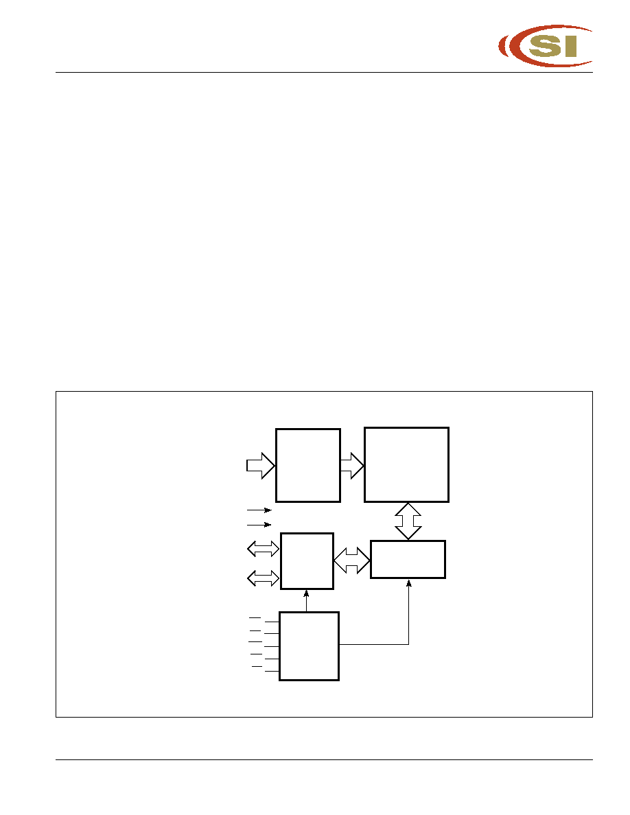
.UNCTIONAL BLOCK DIAGRAM
ICSI reserves the right to make changes to its products at any time without notice in order to improve design and supply the best possible product. We assume no responsibility for any errors
which may appear in this publication. © Copyright 2000, Integrated Circuit Solution Inc.
A0-A15
CE
OE
WE
64K x 16
MEMORY ARRAY
DECODER
COLUMN I/O
CONTROL
CIRCUIT
GND
VCC
I/O
DATA
CIRCUIT
I/O0-I/O7
Lower Byte
I/O8-I/O15
Upper Byte
UB
LB
Integrated Circuit Solution Inc.
1
AHSR011-0A 05/23/2001
1+$+$"$
2
Integrated Circuit Solution Inc.
AHSR011-0A 05/23/2001
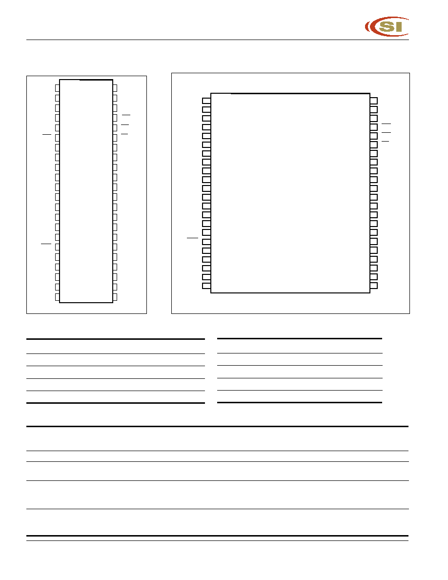
PIN CON.IGURATIONS
44-Pin SOJ
PIN DESCRIPTIONS
A0-A15
Address Inputs
I/O0-I/O15
Data Inputs/Outputs
CE
Chip Enable Input
OE
Output Enable Input
WE
Write Enable Input
TRUTH TABLE
I/O PIN
Mode
WE
WE
WE
WE
WE
CE
CE
CE
CE
CE
OE
OE
OE
OE
OE
LB
LB
LB
LB
LB
UB
UB
UB
UB
UB
I/O0-I/O7
I/O8-I/O15
Vcc Current
Not Selected
X
H
X
X
X
High-Z
High-Z
I
SB
, I
SB
Output Disabled
H
L
H
X
X
High-Z
High-Z
I
CC
, I
CC
X
L
X
H
H
High-Z
High-Z
Read
H
L
L
L
H
D
OUT
High-Z
I
CC
, I
CC
H
L
L
H
L
High-Z
D
OUT
H
L
L
L
L
D
OUT
D
OUT
Write
L
L
X
L
H
D
IN
High-Z
I
CC
, I
CC
L
L
X
H
L
High-Z
D
IN
L
L
X
L
L
D
IN
D
IN
44-Pin TSOP-2
LB
Lower-byte Control (I/O0-I/O7)
UB
Upper-byte Control (I/O8-I/O15)
NC
No Connection
Vcc
Power
GND
Ground
1
2
3
4
5
6
7
8
9
10
11
12
13
14
15
16
17
18
19
20
21
22
44
43
42
41
40
39
38
37
36
35
34
33
32
31
30
29
28
27
26
25
24
23
A15
A14
A13
A12
A11
CE
I/O0
I/O1
I/O2
I/O3
Vcc
GND
I/O4
I/O5
I/O6
I/O7
WE
A10
A9
A8
A7
NC
A0
A1
A2
OE
UB
LB
I/O15
I/O14
I/O13
I/O12
GND
Vcc
I/O11
I/O10
I/O9
I/O8
NC
A3
A4
A5
A6
NC
1+$+$"$
Integrated Circuit Solution Inc.
3
AHSR011-0A 05/23/2001
!
"
#
$
%
&
'
OPERATING RANGE
Range
Ambient Temperature
Speed
V
CC
Commercial
0∞C to +70∞C
-10, -12
5V ± 5%
-15, -20 5V ± 10%
Industrial
40∞C to +85∞C
-12
5V ± 5%
-15, -20 5V ± 10%
POWER SUPPLY CHARACTERISTICS
(1)
(Over Operating Range)
-10
-12
-15
-20
Symbol Parameter
Test Conditions
Min. Max.
Min. Max.
Min. Max.
Min. Max. Unit
I
CC
Vcc Dynamic Operating
V
CC
= Max.,
Com.
300
280
260
235
mA
Supply Current
I
OUT
= 0 mA, f =
MAX
Ind.
300
290
255
I
SB
TTL Standby Current
V
CC
= Max.,
Com.
50
50
50
50
mA
(TTL Inputs)
V
IN
= V
IH
or V
IL
Ind.
55
55
55
CE
V
IH
, f = 0
I
SB
CMOS Standby
V
CC
= Max.,
Com.
10
10
10
10
mA
Current (CMOS Inputs)
CE
V
CC
0.2V,
Ind.
15
15
15
V
IN
V
CC
0.2V, or
V
IN
0.2V, f = 0
Note:
1. At f = f
MAX
, address and data inputs are cycling at the maximum frequency, f = 0 means no input lines change.
DC ELECTRICAL CHARACTERISTICS
(Over Operating Range)
Symbol
Parameter
Test Conditions
Min.
Max.
Unit
V
OH
Output HIGH Voltage
V
CC
= Min., I
OH
= 4.0 mA
2.4
V
V
OL
Output LOW Voltage
V
CC
= Min., I
OL
= 8.0 mA
0.4
V
V
IH
Input HIGH Voltage
(1)
2.2
V
CC
+ 0.5
V
V
IL
Input LOW Voltage
(2)
0.5
0.8
V
I
LI
Input Leakage
GND
V
IN
V
CC
2
2
µA
I
LO
Output Leakage
GND
V
OUT
V
CC
, Outputs Disabled
2
2
µA
Notes:
1. V
IH
=V
CC
+3.0V for pulse width less than 10ns.
2. V
IL
= 3.0V for pulse width less than 10 ns.
ABSOLUTE MAXIMUM RATINGS
(1)
Symbol Parameter
Value
Unit
V
TERM
Terminal Voltage with Respect to GND
0.5 to +7.0
V
T
STG
Storage Temperature
65 to +150
∞C
P
T
Power Dissipation
1.5
W
I
OUT
DC Output Current (LOW)
20
mA
Note:
1. Stress greater than those listed under ABSO-
LUTE MAXIMUM RATINGS may cause per-
manent damage to the device. This is a stress
rating only and functional operation of the
device at these or any other conditions above
those indicated in the operational sections of
this specification is not implied. Exposure to
absolute maximum rating conditions for ex-
tended periods may affect reliability.
1+$+$"$
4
Integrated Circuit Solution Inc.
AHSR011-0A 05/23/2001
READ CYCLE SWITCHING CHARACTERISTICS
(1)
(Over Operating Range)
-10
-12
-15
-20
Symbol
Parameter
Min. Max.
Min. Max.
Min. Max.
Min. Max.
Unit
t
RC
Read Cycle Time
10
12
15
20
ns
t
AA
Address Access Time
10
12
15
20
ns
t
OHA
Output Hold Time
3
3
3
4
ns
t
ACE
CE Access Time
10
12
15
20
ns
t
DOE
OE Access Time
5
6
7
9
ns
t
HZOE
OE to High-Z Output
5
6
0
6
0
8
ns
t
LZOE
OE to Low-Z Output
0
0
0
0
ns
t
HZCE
CE to High-Z Output
0
5
0
6
0
6
0
8
ns
t
LZCE
CE to Low-Z Output
3
3
3
3
ns
t
BA
LB, UB Access Time
5
6
7
9
ns
t
HZB
LB, UB to High-Z Output
0
5
0
6
0
6
0
8
ns
t
LZB
LB, UB to Low-Z Output
0
0
0
0
ns
Notes:
1. Test conditions assume signal transition times of 3 ns or less, timing reference levels of 1.5V, input pulse levels of 0 to 3.0V
and output loading specified in .igure 1.
2. Tested with the load in .igure 2. Transition is measured ±500 mV from steady-state voltage. Not 100% tested.
3. Not 100% tested.
AC TEST CONDITIONS
Parameter
Unit
Input Pulse Level
0V to 3.0V
Input Rise and .all Times
3 ns
Input and Output Timing
1.5V
and Reference Level
Output Load
See .igures 1 and 2
CAPACITANCE
(1)
Symbol
Parameter
Conditions
Max.
Unit
C
IN
Input Capacitance
V
IN
= 0V
6
p.
C
OUT
Input/Output Capacitance
V
OUT
= 0V
8
p.
Note:
1. Tested initially and after any design or process changes that may affect these parameters.
.igure 1
.igure 2
AC TEST LOADS
480
30 pF
Including
jig and
scope
255
OUTPUT
5V
480
5 pF
Including
jig and
scope
255
OUTPUT
5V
1+$+$"$
Integrated Circuit Solution Inc.
5
AHSR011-0A 05/23/2001
!
"
#
$
%
&
'
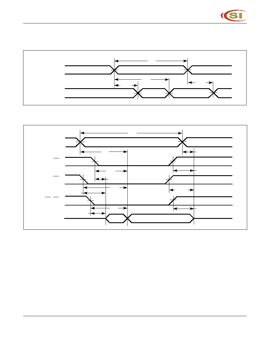
READ CYCLE NO. 2
(1,3)
AC WAVE.ORMS
READ CYCLE NO. 1
(1,2)
(Address Controlled) (CE = OE = V
IL
, UB or LB = V
IL
)
Notes:
1. WE is HIGH for a Read Cycle.
2. The device is continuously selected. OE, CE, UB, or LB = V
IL
.
3. Address is valid prior to or coincident with CE LOW transition.
t
RC
t
OHA
t
AA
t
DOE
t
LZOE
t
ACE
t
LZCE
t
HZOE
HIGH-Z
DATA VALID
t
HZB
ADDRESS
OE
CE
LB, UB
D
OUT
t
HZCE
t
BA
t
LZB
DATA VALID
PREVIOUS DATA VALID
t
AA
t
OHA
t
OHA
t
RC
D
OUT
ADDRESS
1+$+$"$
6
Integrated Circuit Solution Inc.
AHSR011-0A 05/23/2001
WRITE CYCLE SWITCHING CHARACTERISTICS
(1,3)
(Over Operating Range)
-10
-12
-15
-20
Symbol Parameter
Min. Max.
Min. Max.
Min. Max.
Min. Max.
Unit
t
WC
Write Cycle Time
10
12
15
20
ns
t
SCE
CE to Write End
8
9
10
12
ns
t
AW
Address Setup Time
8
9
10
12
ns
to Write End
t
HA
Address Hold from Write End
0
0
0
0
ns
t
SA
Address Setup Time
0
0
0
0
ns
t
PWB
LB, UB Valid to End of Write
8
9
10
12
ns
t
PWE
WE Pulse Width
8
9
10
12
ns
t
SD
Data Setup to Write End
5
6
7
9
ns
t
HD
Data Hold from Write End
0
0
0
0
ns
t
HZWE
WE LOW to High-Z Output
5
6
7
9
ns
t
LZWE
WE HIGH to Low-Z Output
3
3
3
3
ns
Notes:
1. Test conditions assume signal transition times of 3 ns or less, timing reference levels of 1.5V, input pulse levels of 0 to 3.0V
and output loading specified in .igure 1.
2. Tested with the load in .igure 2. Transition is measured ±500 mV from steady-state voltage. Not 100% tested.
3. The internal write time is defined by the overlap of CE LOW and UB or LB, and WE LOW. All signals must be in valid states to
initiate a Write, but any one can go inactive to terminate the Write. The Data Input Setup and Hold timing are referenced to the
rising or falling edge of the signal that terminates the write.
1+$+$"$
Integrated Circuit Solution Inc.
7
AHSR011-0A 05/23/2001
!
"
#
$
%
&
'
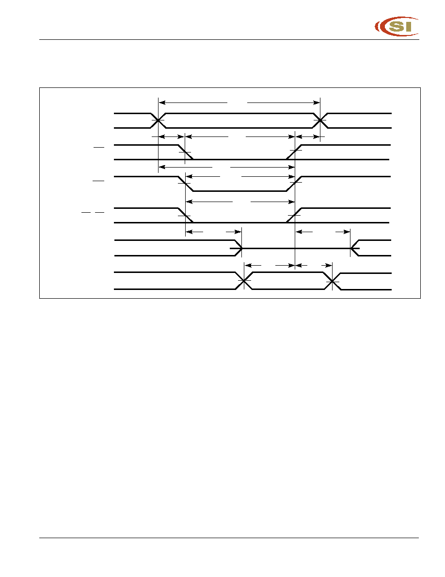
Notes:
1. WRITE is an internally generated signal asserted during an overlap of the LOW states on the CE and WE inputs and at least
one of the LB and UB inputs being in the LOW state.
2. WRITE = (CE)
[
(LB) = (UB)
]
(WE).
AC WAVE.ORMS
WRITE CYCLE NO. 1 (WE
WE
WE
WE
WE Controlled)
(1,2)
DATA UNDEFINED
t
WC
VALID ADDRESS
t
SCE
t
PWE1
t
PWE2
t
AW
t
HA
HIGH-Z
t
PBW
t
HD
t
SA
t
HZWE
ADDRESS
CE
UB, LB
WE
D
OUT
D
IN
DATA
IN
VALID
t
LZWE
t
SD
1+$+$"$
8
Integrated Circuit Solution Inc.
AHSR011-0A 05/23/2001
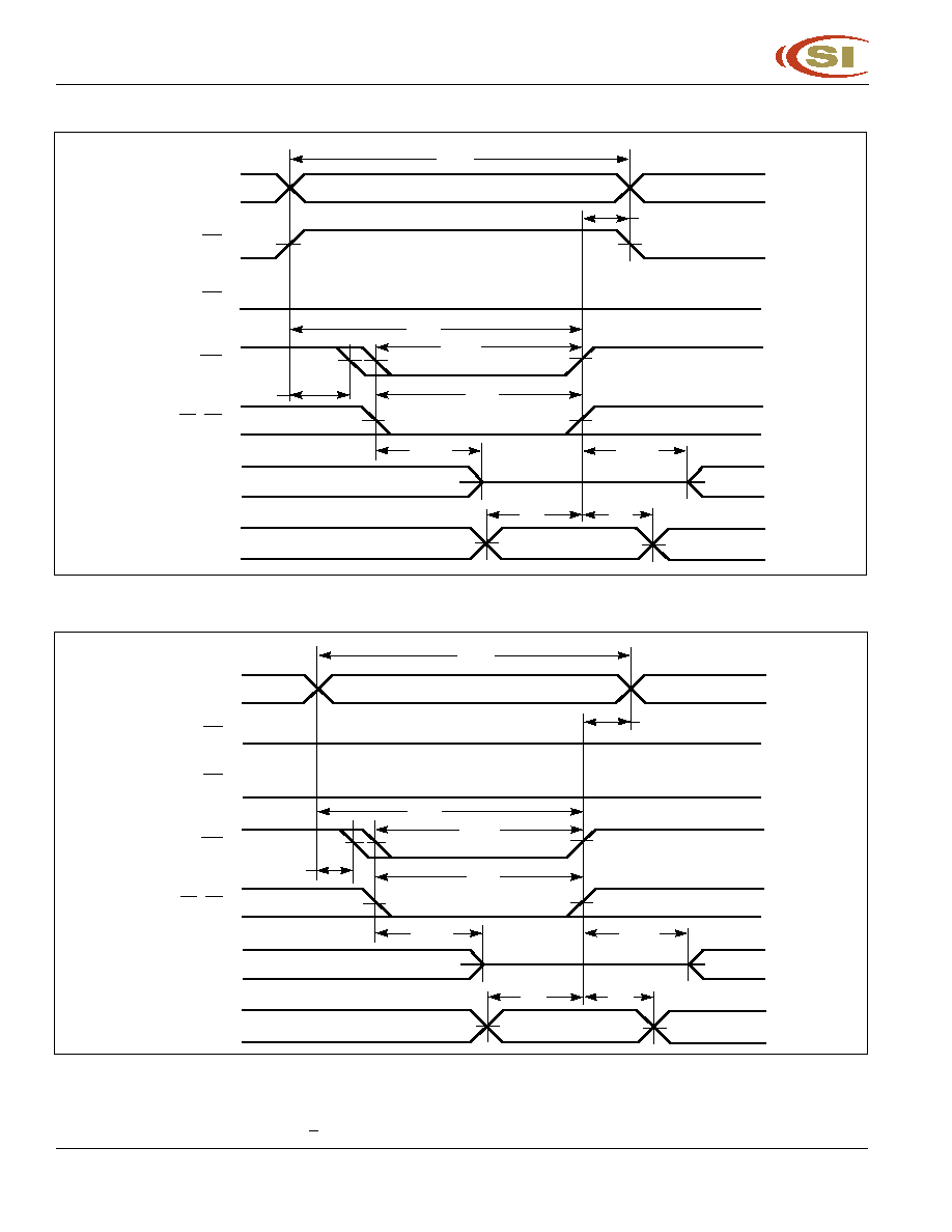
WRITE CYCLE NO. 2
(OE is HIGH During Write Cycle)
(1,2)
WRITE CYCLE NO. 3
(OE is LOW During Write Cycle)
(1)
Notes:
1. The internal write time is defined by the overlap of CE LOW and WE LOW. All signals must be in valid states to initiate a Write,
but any one can go inactive to terminate the Write. The Data Input Setup and Hold timing are referenced to the rising or falling
edge of the signal that terminates the Write.
2. I/O will assume the High-Z state if OE > V
IH
.
DATA UNDEFINED
LOW
t
WC
VALID ADDRESS
t
PWE1
t
AW
t
HA
HIGH-Z
t
PBW
t
HD
t
SA
t
HZWE
ADDRESS
CE
UB, LB
WE
D
OUT
D
IN
OE
DATA
IN
VALID
t
LZWE
t
SD
DATA UNDEFINED
t
WC
VALID ADDRESS
LOW
LOW
t
PWE2
t
AW
t
HA
HIGH-Z
t
PBW
t
HD
t
SA
t
HZWE
ADDRESS
CE
UB, LB
WE
D
OUT
D
IN
OE
DATA
IN
VALID
t
LZWE
t
SD
1+$+$"$
Integrated Circuit Solution Inc.
9
AHSR011-0A 05/23/2001
!
"
#
$
%
&
'
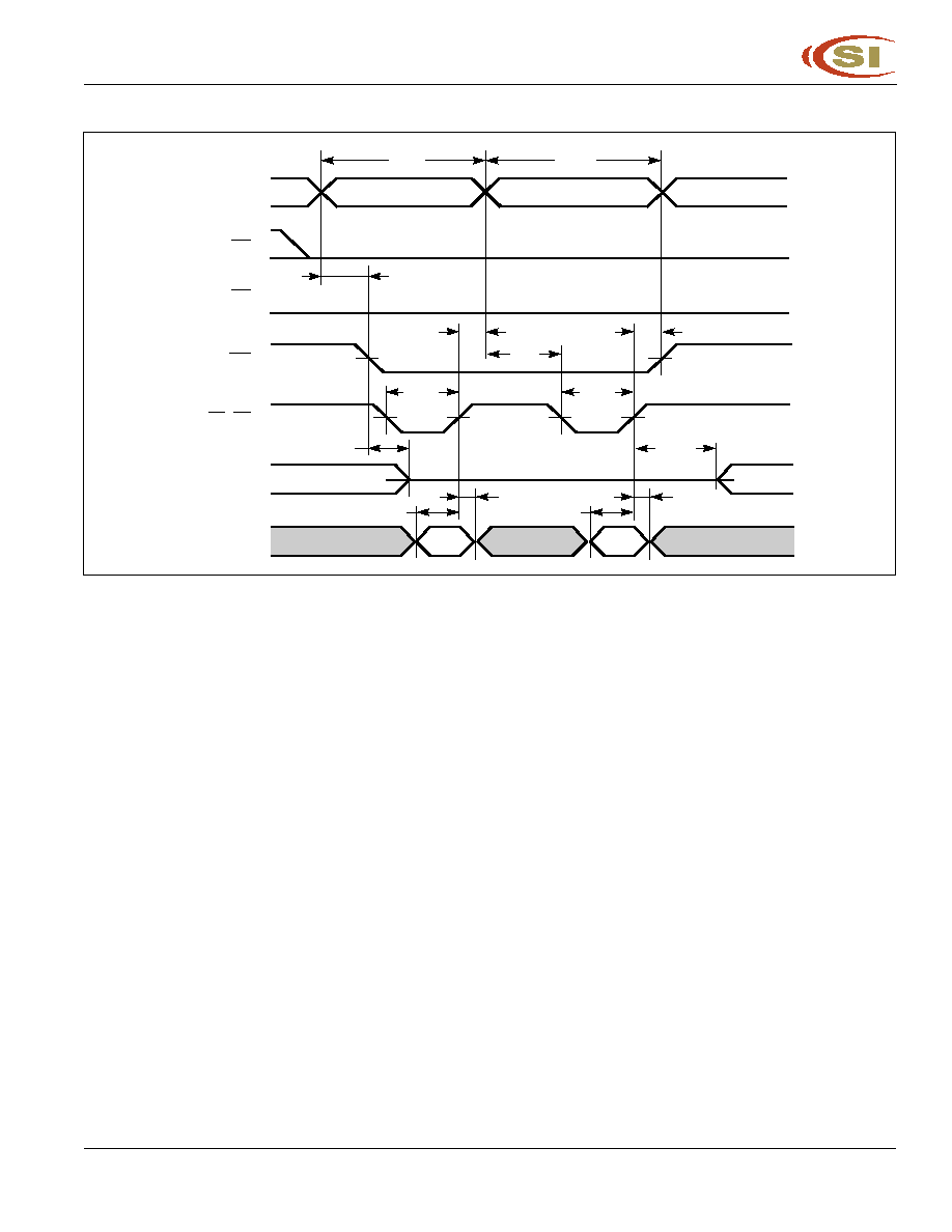
WRITE CYCLE NO. 4
(UB/LB Back to Back Write)
DATA UNDEFINED
t
WC
ADDRESS 1
ADDRESS 2
t
WC
HIGH-Z
t
PBW
WORD 1
LOW
WORD 2
t
HD
t
SA
t
HZWE
ADDRESS
CE
UB, LB
WE
D
OUT
D
IN
OE
DATA
IN
VALID
t
LZWE
t
SD
t
PBW
DATA
IN
VALID
t
SD
t
HD
t
SA
t
HA
t
HA
1+$+$"$
10
Integrated Circuit Solution Inc.
AHSR011-0A 05/23/2001
Integrated Circuit Solution Inc.
HEADQUARTER:
NO.2, TECHNOLOGY RD. V, SCIENCE-BASED INDUSTRIAL PARK,
HSIN-CHU, TAIWAN, R.O.C.
TEL: 886-3-5780333
.ax: 886-3-5783000
BRANCH O..ICE:
7., NO. 106, SEC. 1, HSIN-TAI 5
TH
ROAD,
HSICHIH TAIPEI COUNTY, TAIWAN, R.O.C.
TEL: 886-2-26962140
.AX: 886-2-26962252
http://www.icsi.com.tw
ORDERING IN.ORMATION
Commercial Range: 0∞C to +70∞C
Speed (ns)
Order Part No.
Package
10
IC61C6416-10T
400mil TSOP-2
10
IC61C6416-10K
400mil SOJ
12
IC61C6416-12T
400mil TSOP-2
12
IC61C6416-12K
400mil SOJ
15
IC61C6416-15T
400mil TSOP-2
15
IC61C6416-15K
400mil SOJ
20
IC61C6416-20T
400mil TSOP-2
20
IC61C6416-20K
400mil SOJ
ORDERING IN.ORMATION
Industrial Range: 40∞C to +85∞C
Speed (ns)
Order Part No.
Package
12
IC61C6416-12TI
400mil TSOP-2
12
IC61C6416-12KI
400mil SOJ
15
IC61C6416-15TI
400mil TSOP-2
15
IC61C6416-15KI
400mil SOJ
20
IC61C6416-20TI
400mil TSOP-2
20
IC61C6416-20KI
400mil SOJ