
IC61LV25616
Integrated Circuit Solution Inc.
1
AHSR022-0A
09/11/2001
1
2
3
4
5
6
7
8
9
10
11
12
Document Title
256K x 16 Hight Speed SRAM with 3.3V
Revision History
Revision No
History
Draft Date
Remark
0A
Initial Draft
September 11,2001
The attached datasheets are provided by ICSI. Integrated Circuit Solution Inc reserve the right to change the specifications and
products. ICSI will answer to your questions about device. If you have any questions, please contact the ICSI offices.
IC61LV25616
2
Integrated Circuit Solution Inc.
AHSR022-0A
09/11/2001
FEATURES
∑ High-speed access time: 8, 10, 12, and 15 ns
∑ CMOS low power operation
∑ TTL compatible interface levels
∑ Single 3.3V
±
10% power supply
∑ Fully static operation: no clock or refresh
required
∑ Three state outputs
∑ Data control for upper and lower bytes
∑ Industrial temperature available
256K x 16 HIGH SPEED ASYNCHRONOUS
CMOS STATIC RAM WITH 3.3V SUPPLY
DESCRIPTION
The
ICSI
IC61LV25616 is a high-speed, 4,194,304-bit static
RAM organized as 262,144 words by 16 bits. It is fabricated
using
ICSI
's high-performance CMOS technology. This highly
reliable process coupled with innovative circuit design
techniques, yields high-performance and low power consump-
tion devices.
When
CE
is HIGH (deselected), the device assumes a standby
mode at which the power dissipation can be reduced down with
CMOS input levels.
Easy memory expansion is provided by using Chip Enable and
Output Enable inputs,
CE
and
OE
. The active LOW Write
Enable (
WE
) controls both writing and reading of the memory.
A data byte allows Upper Byte (
UB
) and Lower Byte (
LB
)
access.
The IC61LV25616 is packaged in the JEDEC standard
44-pin 400mil SOJ, 44 pin 400mil TSOP-2 and 48-pin 6*8 TF-
BGA.
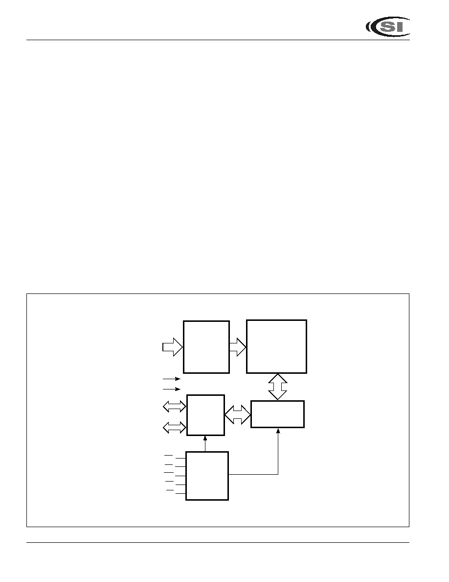
FUNCTIONAL BLOCK DIAGRAM
ICSI reserves the right to make changes to its products at any time without notice in order to improve design and supply the best possible product. We assume no responsibility for any errors
which may appear in this publication. © Copyright 2000, Integrated Circuit Solution Inc.
A0-A17
CE
OE
WE
256K x 16
MEMORY ARRAY
DECODER
COLUMN I/O
CONTROL
CIRCUIT
GND
VCC
I/O
DATA
CIRCUIT
I/O0-I/O7
Lower Byte
I/O8-I/O15
Upper Byte
UB
LB
IC61LV25616
Integrated Circuit Solution Inc.
3
AHSR022-0A
09/11/2001
1
2
3
4
5
6
7
8
9
10
11
12
PIN DESCRIPTIONS
A0-A17
Address Inputs
I/O0-I/O15
Data Inputs/Outputs
CE
Chip Enable Input
OE
Output Enable Input
WE
Write Enable Input
TRUTH TABLE
I/O PIN
Mode
WE
WE
WE
WE
WE
CE
CE
CE
CE
CE
OE
OE
OE
OE
OE
LB
LB
LB
LB
LB
UB
UB
UB
UB
UB
I/O0-I/O7
I/O8-I/O15
Vcc Current
Not Selected
X
H
X
X
X
High-Z
High-Z
I
SB
1
, I
SB
2
Output Disabled
H
L
H
X
X
High-Z
High-Z
I
CC
X
L
X
H
H
High-Z
High-Z
Read
H
L
L
L
H
D
OUT
High-Z
I
CC
H
L
L
H
L
High-Z
D
OUT
H
L
L
L
L
D
OUT
D
OUT
Write
L
L
X
L
H
D
IN
High-Z
I
CC
L
L
X
H
L
High-Z
D
IN
L
L
X
L
L
D
IN
D
IN
LB
Lower-byte Control (I/O0-I/O7)
UB
Upper-byte Control (I/O8-I/O15)
NC
No Connection
Vcc
Power
GND
Ground
1
2
3
4
5
6
7
8
9
10
11
12
13
14
15
16
17
18
19
20
21
22
44
43
42
41
40
39
38
37
36
35
34
33
32
31
30
29
28
27
26
25
24
23
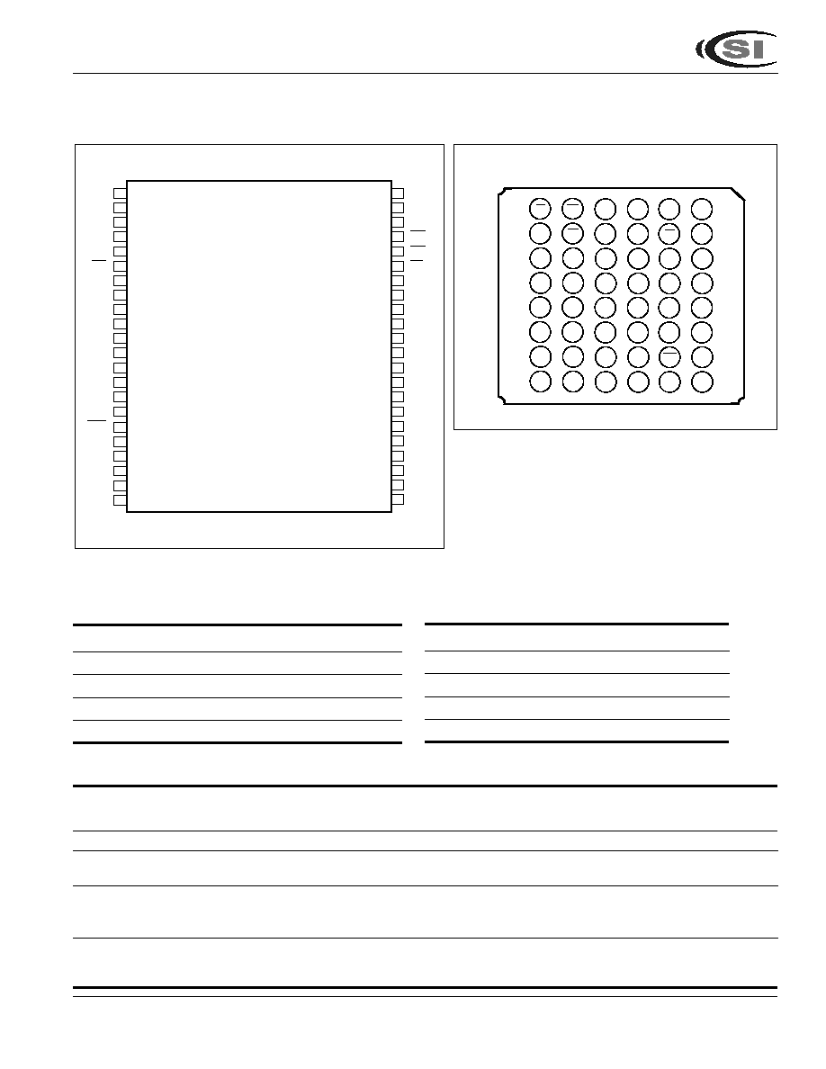
A0
A1
A2
A3
A4
CE
I/O0
I/O1
I/O2
I/O3
Vcc
GND
I/O4
I/O5
I/O6
I/O7
WE
A5
A6
A7
A8
A9
A17
A16
A15
OE
UB
LB
I/O15
I/O14
I/O13
I/O12
GND
Vcc
I/O11
I/O10
I/O9
I/O8
NC
A14
A13
A12
A11
A10
PIN CONFIGURATIONS
44-Pin TSOP-2 and SOJ
48-Pin TF-BGA
1 2 3 4 5 6
A
B
C
D
E
F
G
H
LB
OE
A0
A1
A2
N/C
I/O
0
UB
A3
A4
CE
I/O
8
I/O
1
I/O
2
A5
A6
I/O
10
I/O
9
GND
I/O
3
A17
A7
I/O
11
Vcc
Vcc
I/O
4
NC
A16
I/O
12
GND
I/O
6
I/O
5
A14
A15
I/O
13
I/O
14
I/O
7
NC
A12
A13
WE
I/O
15
NC
A8
A9
A10
A11
NC
IC61LV25616
4
Integrated Circuit Solution Inc.
AHSR022-0A
09/11/2001
OPERATING RANGE
Range
Ambient Temperature
V
CC
Commercial
0∞C to +70∞C
3.3V
±
10%
Industrial
≠40∞C to +85∞C
3.3V
±
10%
DC ELECTRICAL CHARACTERISTICS
(Over Operating Range)
Symbol
Parameter
Test Conditions
Min.
Max.
Unit
V
OH
Output HIGH Voltage
V
CC
= Min., I
OH
= ≠4.0 mA
2.4
--
V
V
OL
Output LOW Voltage
V
CC
= Min., I
OL
= 8.0 mA
--
0.4
V
V
IH
Input HIGH Voltage
2.0
V
CC
+ 0.3
V
V
IL
Input LOW Voltage
(1)
≠0.3
0.8
V
I
LI
Input Leakage
GND
V
IN
V
CC
Com.
≠1
1
µA
Ind.
≠5
5
I
LO
Output Leakage
GND
V
OUT
V
CC
Com.
≠1
1
µA
Outputs Disabled
Ind.
≠5
5
Notes:
1. V
IL
(min.) = ≠2.0V for pulse width less than 10 ns.
2. The Vcc operating range for 8 ns is 3.3V +10%, -5%.
POWER SUPPLY CHARACTERISTICS
(1)
(Over Operating Range)
-8 ns
-10 ns
-12 ns
-15 ns
Symbol
Parameter
Test Conditions
Min. Max.
Min. Max.
Min. Max.
Min. Max. Unit
I
CC
Vcc Dynamic Operating
V
CC
= Max.,
Com.
--
350
--
320
--
290
--
260
mA
Supply Current
I
OUT
= 0 mA, f = f
MAX
Ind.
--
360
--
330
--
300
--
270
I
SB
1
TTL Standby Current
V
CC
= Max.,
Com.
--
55
--
55
--
55
--
55
mA
(TTL Inputs)
V
IN
= V
IH
or V
IL
Ind.
--
65
--
65
--
65
--
65
CE
V
IH
, f = 0
I
SB
2
CMOS Standby
V
CC
= Max.,
Com.
--
10
--
10
--
10
--
10
mA
Current (CMOS Inputs)
CE
V
CC
≠ 0.2V,
Ind.
--
15
--
15
--
15
--
15
V
IN
V
CC
≠ 0.2V, or
V
IN
0.2V, f = 0
Note:
1. At f = f
MAX
, address and data inputs are cycling at the maximum frequency, f = 0 means no input lines change.
ABSOLUTE MAXIMUM RATINGS
(1)
Symbol Parameter
Value
Unit
V
TERM
Terminal Voltage with Respect to GND
≠0.5 to Vcc+0.5
V
T
BIAS
Temperature Under Bias
≠45 to +90
∞C
V
CC
Vcc Related to GND
≠0.3 to +4.0
V
T
STG
Storage Temperature
≠65 to +150
∞C
P
T
Power Dissipation
1.0
W
Note:
1. Stress greater than those listed under
ABSOLUTE MAXIMUM RATINGS may
cause permanent damage to the device.
This is a stress rating only and func-
tional operation of the device at these
or any other conditions above those
indicated in the operational sections of
this specification is not implied. Expo-
sure to absolute maximum rating con-
ditions for extended periods may affect
reliability.
IC61LV25616
Integrated Circuit Solution Inc.
5
AHSR022-0A
09/11/2001
1
2
3
4
5
6
7
8
9
10
11
12
AC TEST CONDITIONS
Parameter
Unit
Input Pulse Level
0V to 3.0V
Input Rise and Fall Times
3 ns
Input and Output Timing
1.5V
and Reference Level
Output Load
See Figures 1 and 2
Notes:
1. The Vcc operating range for 8 ns is 3.3V +10%, -5%.
CAPACITANCE
(1)
Symbol
Parameter
Conditions
Max.
Unit
C
IN
Input Capacitance
V
IN
= 0V
6
pF
C
OUT
Input/Output Capacitance
V
OUT
= 0V
8
pF
Note:
1. Tested initially and after any design or process changes that may affect these parameters.
READ CYCLE SWITCHING CHARACTERISTICS
(1)
(Over Operating Range)
-8
-10
-12
-15
Symbol
Parameter
Min.
Max.
Min.
Max.
Min.
Max.
Min.
Max.
Unit
t
RC
Read Cycle Time
8
--
10
--
12
--
15
--
ns
t
AA
Address Access Time
--
8
--
10
--
12
--
15
ns
t
OHA
Output Hold Time
3
--
3
--
3
--
3
--
ns
t
ACE
CE
Access Time
--
8
--
10
--
12
--
15
ns
t
DOE
OE
Access Time
--
4
--
5
--
6
--
7
ns
t
HZOE
(2)
OE
to High-Z Output
0
4
--
5
--
6
0
6
ns
t
LZOE
(2)
OE
to Low-Z Output
0
--
0
--
0
--
0
--
ns
t
HZCE
(2
CE
to High-Z Output
0
4
0
5
0
6
0
6
ns
t
LZCE
(2)
CE
to Low-Z Output
3
--
3
--
3
--
3
--
ns
t
BA
LB
,
UB
Access Time
--
4
--
5
--
6
--
7
ns
t
HZB
LB
,
UB
to High-Z Output
0
4
0
5
0
6
0
6
ns
t
LZB
LB
,
UB
to Low-Z Output
0
--
0
--
0
--
0
--
ns
Notes:
1. Test conditions assume signal transition times of 3 ns or less, timing reference levels of 1.5V, input pulse levels of
0 to 3.0V and output loading specified in Figure 1a.
2. Tested with the load in Figure 1b. Transition is measured ±500 mV from steady-state voltage. Not 100% tested.
3. Not 100% tested.
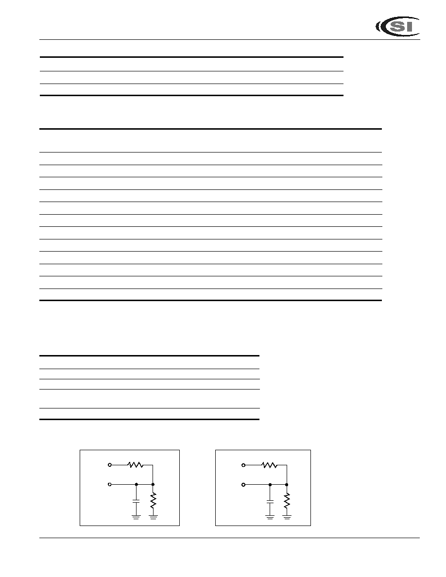
AC TEST LOADS
Figure 1
Figure 2
319
30 pF
Including
jig and
scope
353
OUTPUT
3.3V
319
5 pF
Including
jig and
scope
353
OUTPUT
3.3V