
IC61S25632T/D IC61S25636T/D
IC61S51218T/D
Integrated Circuit Solution Inc.
1
SSR014-0B 08/13/2002
Document Title
8Mb SyncBurst Pipelined SRAM
Revision History
Revision No
History
Draft Date
Remark
0A
Initial Draft
September 24,2001
0B
1. Move the
FT
pin for user-configurable Flow
August 13,2002
throught or pipelineed operation, That pin can be
NC or connected to V
CC
for pipelined operation.
Refer to Pin configuration.
2. Revise the power supply charaetoristics at page 12
3. Resive the t
KQ
of 250 MHZ from 2.5ns to 3ns.
4. Move the 100 MHZ speed grade.
The attached datasheets are provided by ICSI. Integrated Circuit Solution Inc reserve the right to change the specifications and
products. ICSI will answer to your questions about device. If you have any questions, please contact the ICSI offices.

IC61S25632T/D IC61S25636T/D
IC61S51218T/D
2
Integrated Circuit Solution Inc.
SSR014-0B 08/13/2002
ICSI reserves the right to make changes to its products at any time without notice in order to improve design and supply the best possible product. We assume no responsibility for any errors
which may appear in this publication. © Copyright 2000, Integrated Circuit Solution Inc.
FEATURES
∑ Pipeline Mode operation
∑ Single/Dual Cycl Deselect
∑ User-selectable Output Drive Strength with XQ Mode
∑ Internal self-timed write cycle
∑ Individual Byte Write Control and Global Write
∑ Clock controlled, registered address, data and control
∑ PentiumTM or linear burst sequence control using
MODE input
∑ Common data inputs and data outputs
∑ JEDEC 100-Pin TQFP and 119-pin PBGA package
∑ Single +3.3V, +10%, ≠5% core power supply
∑ Power-down snooze mode
∑ 2.5V or 3.3V I/O Supply
∑ Snooze MODE for reduced-power standby
∑ T version (three chip selects)
∑ D version (two chip selects)
DESCRIPTION
ICSI's 8Mb SyncBurst Pipelined SRAMs integrate a 512k
x 18, 256k x 32, or 256k x 36 SRAM core with advanced
synchronous peripheral circuitry and a 2-bit burst counter.
Applications
Applications
Applications
Applications
Applications
The ICSI SyncBurst Pipelined SRAM family employs
high-speed ,low-power CMOS designs that are fabricated
using an advanced CMOS process to provide Level 2
Cache applications supporting Pentium and PowerPC
microprocessors originally, the device now finds applica-
tion ranging from DSP main store to networking chip set
support.
256K x 32, 256K x 36, 512K x 18
8Mb S/DCD SYNCBURST Pipelined SRAMs
Controls
All synchronous inputs pass through registers controlled by a
positive-edge-triggered single clock input.Bursts can be initiated
with either
ADSP
(Address Status Processor) or
ADSC
(Address
Status Cache Controller) input pins. Subsequent burst ad-
dresses can be generated internally and controlled by the
ADV
(burst address advance) input pin. The mode pin is used to select
the burst sequence order, Linear burst is achieved when this pin
is tied LOW. Interleave burst is achieved when this pin is tied
HIGH or left floating.
SCD and DCD Pipelined Reads
The device is a SCD (Single Cycle Deselect) and DCD(Dual
Cycle Deselect) pipelined synchronous SRAM. DCD SRAMs
pipeline disable commands to the same degree as read
commands. SCD SRAMs pipeline deselect commands one
stage less than read commands. SCD RAMs begin turning off
their outputs immediately after the deselect command has been
captured in the input registers. DCD RAMs hold the deselect
command for one full cycle and then begin turning off their
outputs just after the second rising edge of clock. The user may
configure this SRAM for either mode of operation using the SCD
mode input on Bump 4L.
Byte Write and Global Write
Write cycles are internally self-timed and are initiated by the rising
edge of the clock input. Write cycles can be from one to four bytes
wide as controlled by the write control inputs.Separate byte
enables allow individual bytes to be written. Byte write operation
is performed by using byte write enable (
BWE
).input combined
with one or more individualbyte write signals (
BWx
). In addition,
Global Write (
GW)
is available for writing all bytes at one time,
regardless of the byte write controls.
IOL/IOH Drive strength Options
The XQ pin allows selection between high drive strength (XQ
low) for multi-drop bus applications and normal drive strength
(XQ floating or high) point-to-point applications. See the Output
Driver Characteristics chart for details.
Snooze Mode
Low power (Snooze mode) is attained through the assertion
(High) of the ZZ signal, or by stopping the clock (CK). Memory
data is retained during Snooze mode.
FAST ACCESS TIME
Symbol
-250
-200
-166
-133
Units
Pipeline
t
KQ
3
3.1
3.5
4
ns
3-1-1-1
t
KC
4
5
6
7.5
ns
I
CC
1
390
360
330
300
mA
IC61S25632T/D IC61S25636T/D
IC61S51218T/D
Integrated Circuit Solution Inc.
3
SSR014-0B 08/13/2002
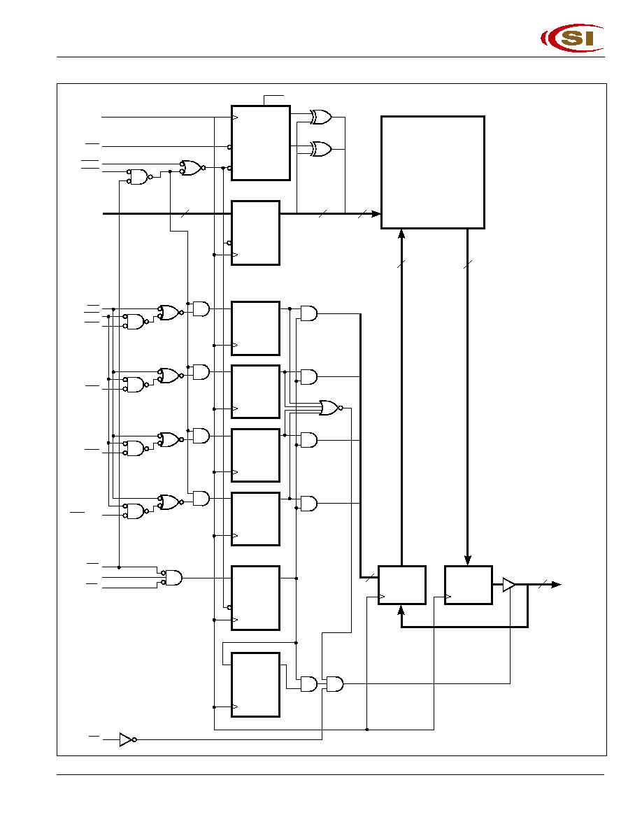
BLOCK DIAGRAM
18/19
BINARY
COUNTER
GW
CLK
Q0
Q1
MODE
A0'
A0
A1
A1'
CLK
ADV
ADSC
ADSP
16/17
18/19
ADDRESS
REGISTER
D
CLK
Q
DQd
BYTE WRITE
REGISTERS
D
CLK
Q
DQc
BYTE WRITE
REGISTERS
D
CLK
Q
DQb
BYTE WRITE
REGISTERS
D
CLK
Q
DQa
BYTE WRITE
REGISTERS
D
CLK
Q
ENABLE
REGISTER
D
CLK
Q
ENABLE
DELAY
REGISTER
D
CLK
Q
BWE
BWd
(T, D)CE
(T) CE
2
(T, D) CE2
BWa
BWb
256Kx32; 256Kx36;
512Kx18
MEMORY ARRAY
32, 36,
or 18
INPUT
REGISTERS
CLK
OUTPUT
REGISTERS
CLK
OE
4
OE
DQa - DQd
32, 36,
or 18
32, 36,
or 18
An-A0
(x32/x36)
(x32/x36/x18)
(x32/x36)
(x32/x36/x18)
BWa
IC61S25632T/D IC61S25636T/D
IC61S51218T/D
4
Integrated Circuit Solution Inc.
SSR014-0B 08/13/2002
NC
DQb8
DQb7
VCCQ
GND
DQb6
DQb5
DQb4
DQb3
GND
VCCQ
DQb2
DQb1
GND
SCD
VCC
ZZ
DQa8
DQa7
VCCQ
GND
DQa6
DQa5
DQa4
DQa3
GND
VCCQ
DQa2
DQa1
NC
SA
SA
CE
CE2
BWd
BWc
BWb
BWa
SA
VCC
GND
CLK
GW
BWE
OE
ADSC
ADSP
ADV
SA
SA
NC
DQc1
DQc2
VCCQ
GND
DQc3
DQc4
DQc5
DQc6
GND
VCCQ
DQc7
DQc8
VCC
XQ
GND
DQd1
DQd2
VCCQ
GND
DQd3
DQd4
DQd5
DQd6
GND
VCCQ
DQd7
DQd8
NC
1
2
3
4
5
6
7
8
9
10
11
12
13
14
15
16
17
18
19
20
21
22
23
24
25
26
27
28
29
30
80
79
78
77
76
75
74
73
72
71
70
69
68
67
66
65
64
63
62
61
60
59
58
57
56
55
54
53
52
51
100 99 98 97 96 95 94 93 92 91 90 89 88 87 86 85 84 83 82 81
31 32 33 34 35 36 37 38 39 40 41 42 43 44 45
MODE
SA
SA
SA
SA
A1
A0
NC
NC
GND
VCC
NC
NC
A10
SA
SA
SA
SA
SA
SA
46 47 48 49 50
NC
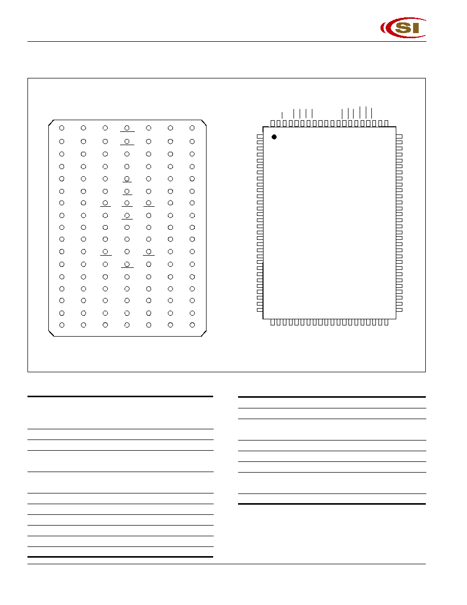
PIN CONFIGURATION
119-pin PBGA (Top View)
100-Pin TQFP (D Version)
256K x 32
PIN DESCRIPTIONS
A0, A1
Synchronous Address Inputs. These
pins must tied to the two LSBs of the
address bus.
A2-A17
Synchronous Address Inputs
CLK
Synchronous Clock
ADSP
Synchronous Processor Address
Status
ADSC
Synchronous Controller Address
Status
ADV
Synchronous Burst Address Advance
BWa
-
BWd
Synchronous Byte Write Enable
BWE
Synchronous Byte Write Enable
GW
Synchronous Global Write Enable
CE
, CE2
Synchronous Chip Enable
OE
Output Enable
DQa-DQd
Synchronous Data Input/Output
MODE
Burst Sequence Mode Selection
SCD
Single Cycle Deselect/Dual Cycle
Deselect Mode Control
XQ
Output Drive Control
V
CC
+3.3V Power Supply
GND
Ground
V
CCQ
Isolated Output Buffer Supply : +3.3V
or 2.5V
ZZ
Snooze Enable
A
B
C
D
E
F
G
H
J
K
L
M
N
P
R
T
U
VCCQ
NC
NC
DQc1
DQc2
VCCQ
DQc5
DQc7
VCCQ
DQd1
DQd4
VCCQ
DQd6
DQd8
NC
NC
VCCQ
SA
CE2
SA
NC
DQc3
DQc4
DQc6
DQc8
VCC
DQd2
DQd3
DQd5
DQd7
NC
SA
NC
NC
SA
SA
SA
GND
GND
GND
BWc
GND
NC
GND
BWd
GND
GND
GND
MODE
SA
NC
ADSP
ADSC
VCC
XQ
CE
OE
ADV
GW
VCC
CLK
SCD
BWE
A1
A0
VCC
SA
NC
SA
SA
SA
GND
GND
GND
BWb
GND
NC
GND
BWa
GND
GND
GND
NC
SA
NC
SA
SA
SA
NC
DQb6
DQb5
DQb4
DQb2
VCC
DQa7
DQa5
DQa4
DQa3
NC
SA
NC
NC
VCCQ
NC
NC
DQb8
DQb7
VCCQ
DQb3
DQb1
VCCQ
DQa8
DQa6
VCCQ
DQa2
DQa1
NC
ZZ
VCCQ
1 2 3 4 5 6 7
Note:Ball R5 connecting to V
CC
is acceptable Note:pin 14 connecting to V
CC
is acceptable

IC61S25632T/D IC61S25636T/D
IC61S51218T/D
Integrated Circuit Solution Inc.
5
SSR014-0B 08/13/2002
NC
DQb8
DQb7
VCCQ
GND
DQb6
DQb5
DQb4
DQb3
GND
VCCQ
DQb2
DQb1
GND
SCD
VCC
ZZ
DQa8
DQa7
VCCQ
GND
DQa6
DQa5
DQa4
DQa3
GND
VCCQ
DQa2
DQa1
NC
SA
SA
CE
CE2
BWd
BWc
BWb
BWa
CE2
VCC
GND
CLK
GW
BWE
OE
ADSC
ADSP
ADV
SA
SA
NC
DQc1
DQc2
VCCQ
GND
DQc3
DQc4
DQc5
DQc6
GND
VCCQ
DQc7
DQc8
NC
VCC
XQ
GND
DQd1
DQd2
VCCQ
GND
DQd3
DQd4
DQd5
DQd6
GND
VCCQ
DQd7
DQd8
NC
1
2
3
4
5
6
7
8
9
10
11
12
13
14
15
16
17
18
19
20
21
22
23
24
25
26
27
28
29
30
80
79
78
77
76
75
74
73
72
71
70
69
68
67
66
65
64
63
62
61
60
59
58
57
56
55
54
53
52
51
100 99 98 97 96 95 94 93 92 91 90 89 88 87 86 85 84 83 82 81
31 32 33 34 35 36 37 38 39 40 41 42 43 44 45
MODE
SA
SA
SA
SA
A1
A0
NC
NC
GND
VCC
NC
SA
SA
SA
SA
SA
SA
SA
SA
46 47 48 49 50
PIN CONFIGURATION
100-Pin TQFP (T Version)
256K x 32
PIN DESCRIPTIONS
A0, A1
Synchronous Address Inputs. These
pins must tied to the two LSBs of the
address bus.
A2-A17
Synchronous Address Inputs
CLK
Synchronous Clock
ADSP
Synchronous Processor Address
Status
ADSC
Synchronous Controller Address
Status
ADV
Synchronous Burst Address Advance
BWa
-
BWd
Synchronous Byte Write Enable
BWE
Synchronous Byte Write Enable
GW
Synchronous Global Write Enable
CE
,CE2,
CE2
Synchronous Chip Enable
OE
Output Enable
DQa-DQd
Synchronous Data Input/Output
MODE
Burst Sequence Mode Selection
SCD
Single Cycle Deselect/Dual Cycle
Deselect Mode Control
XQ
Output Drive Control
V
CC
+3.3V Power Supply
GND
Ground
V
CCQ
Isolated Output Buffer Supply : +3.3V
or 2.5V
ZZ
Snooze Enable
Note:Pin 14 connecting to Vcc is acceptable