
Integrated Circuit Solution Inc.
1
SSR019-0A
09/17/2001
IC61SP12832
IC61SP12836
Document Title
128K x 32 Pipelined SyncBurst SRAM
Revision History
Revision No
History
Draft Date
Remark
0A
Initial Draft
September 17,2001
The attached datasheets are provided by ICSI. Integrated Circuit Solution Inc reserve the right to change the specifications and
products. ICSI will answer to your questions about device. If you have any questions, please contact the ICSI offices.
2
Integrated Circuit Solution Inc.
SSR019-0A
09/17/2001
IC61SP12832
IC61SP12836
ICSI reserves the right to make changes to its products at any time without notice in order to improve design and supply the best possible product. We assume no responsibility for any errors
which may appear in this publication. � Copyright 2000, Integrated Circuit Solution Inc.
FEATURES
� Internal self-timed write cycle
� Individual Byte Write Control and Global Write
� Clock controlled, registered address, data and
control
� PentiumTM or linear burst sequence control
using MODE input
� Three chip enables for simple depth expansion
and address pipelining
� Common data inputs and data outputs
� 100-Pin TQFP (JEDEC LQFP) and
119-pin PBGA package
� Single +3.3V, +10%, �5% power supply
� Power-down snooze mode
DESCRIPTION
The
ICSI
IC61SP12832,IC61SP12836 are high-speed, low-
power synchronous static RAM designed to provide a burstable,
high-performance, secondary cache for the PentiumTM, 680X0TM,
and PowerPCTM microprocessors. It is organized as 131,072
words by 32 bits, fabricated with
ICSI
's advanced CMOS
technology. The device integrates a 2-bit burst counter, high-
speed SRAM core, and high-drive capability outputs into a
single monolithic circuit. All synchronous inputs pass through
registers controlled by a positive-edge-triggered single clock
input.
Write cycles are internally self-timed and are initiated by the
rising edge of the clock input. Write cycles can be from one to
four bytes wide as controlled by the write control inputs.
Separate byte enables allow individual bytes to be written.
BW1
controls DQa,
BW2
controls DQb,
BW3
controls DQc,
BW4
controls DQd, conditioned by
BWE
being LOW. A LOW
on
GW
input would cause all bytes to be written.
Bursts can be initiated with either
ADSP
(Address Status
Processor) or
ADSC
(Address Status Cache Controller) input
pins. Subsequent burst addresses can be generated internally
by the IC61SP12832,IC61SP12836 and controlled by the
ADV
(burst address advance) input pin.
The mode pin is used to select the burst sequence order,
Linear burst is achieved when this pin is tied LOW. Interleave
burst is achieved when this pin is tied HIGH or left floating.
128K x 32, 128K x 36 SYNCHRONOUS
PIPELINED STATIC RAM
FAST ACCESS TIME
Symbol
Parameter
-166
-150
-133
-117
-5
Units
t
KQ
Clock Access Time
3.5
3.8
4
4
5
ns
t
KC
Cycle Time
6
6.7
7.5
8.5
10
ns
Frenquency
166
150
133
117
100
MHz
Integrated Circuit Solution Inc.
3
SSR019-0A
09/17/2001
IC61SP12832
IC61SP12836
BLOCK DIAGRAM
17
BINARY
COUNTER
A16-A0
BW1
GW
CLR
CE
CLK
Q0
Q1
MODE
A0'
A0
A1
A1'
CLK
ADV
ADSC
ADSP
15
17
ADDRESS
REGISTER
CE
D
CLK
Q
DQd
BYTE WRITE
REGISTERS
D
CLK
Q
DQc
BYTE WRITE
REGISTERS
D
CLK
Q
DQb
BYTE WRITE
REGISTERS
D
CLK
Q
DQa
BYTE WRITE
REGISTERS
D
CLK
Q
ENABLE
REGISTER
CE
D
CLK
Q
ENABLE
DELAY
REGISTER
D
CLK
Q
BWE
BW4
CE
CE2
CE2
BW2
BW3
128K x 32, 128K x 36
MEMORY
ARRAY
32
INPUT
REGISTERS
CLK
OUTPUT
REGISTERS
CLK
32
OE
4
32
OE
DQ[31:0]
4
Integrated Circuit Solution Inc.
SSR019-0A
09/17/2001
IC61SP12832
IC61SP12836
PIN CONFIGURATION
119-pin PBGA (Top View) and 100-Pin LQFP
PIN DESCRIPTIONS
A0, A1
Synchronous Address Inputs. These
pins must tied to the two LSBs of the
address bus.
A2-A16
Synchronous Address Inputs
CLK
Synchronous Clock
ADSP
Synchronous Processor Address
Status
ADSC
Synchronous Controller Address
Status
ADV
Synchronous Burst Address Advance
BW1
-
BW4
Synchronous Byte Write Enable
BWE
Synchronous Byte Write Enable
GW
Synchronous Global Write Enable
CE
,
CE2
, CE2 Synchronous Chip Enable
OE
Output Enable
DQa-DQd
Synchronous Data Input/Output
MODE
Burst Sequence Mode Selection
V
CC
+3.3V Power Supply
GND
Ground
V
CCQ
Isolated Output Buffer Supply:
+3.3V
ZZ
Snooze Enable
GND
Q
Isolated Output Buffer Ground
A
B
C
D
E
F
G
H
J
K
L
M
N
P
R
T
U
VCCQ
NC
NC
DQc1
DQc2
VCCQ
DQc5
DQc7
VCCQ
DQd1
DQd4
VCCQ
DQd6
DQd8
NC
NC
VCCQ
A6
CE2
A7
NC
DQc3
DQc4
DQc6
DQc8
VCC
DQd2
DQd3
DQd5
DQd7
NC
A5
NC
NC
A4
A3
A2
GND
GND
GND
BW3
GND
NC
GND
BW4
GND
GND
GND
MODE
A10
NC
ADSP
ADSC
VCC
NC
CE
OE
ADV
GW
VCC
CLK
NC
BWE
A1
A0
VCC
A11
NC
A8
A9
A12
GND
GND
GND
BW2
GND
NC
GND
BW1
GND
GND
GND
NC
A14
NC
A16
CE2
A15
NC
DQb6
DQb5
DQb4
DQb2
VCC
DQa7
DQa5
DQa4
DQa3
NC
A13
NC
NC
VCCQ
NC
NC
DQb8
DQb7
VCCQ
DQb3
DQb1
VCCQ
DQa8
DQa6
VCCQ
DQa2
DQa1
NC
ZZ
VCCQ
1 2 3 4 5 6 7
NC
DQb8
DQb7
VCCQ
GND
DQb6
DQb5
DQb4
DQb3
GND
VCCQ
DQb2
DQb1
GND
NC
VCC
ZZ
DQa8
DQa7
VCCQ
GND
DQa6
DQa5
DQa4
DQa3
GND
VCC
DQa2
DQa1
NC
A6
A7
CE
CE2
BW4
BW3
BW2
BW1
CE2
VCC
GND
CLK
GW
BWE
OE
ADSC
ADSP
ADV
A8
A9
NC
DQc1
DQc2
VCCQ
GND
DQc3
DQc4
DQc5
DQc6
GND
VCCQ
DQc7
DQc8
NC
VCC
NC
GND
DQd1
DQd2
VCCQ
GND
DQd3
DQd4
DQd5
DQd6
GND
VCCQ
DQd7
DQd8
NC
1
2
3
4
5
6
7
8
9
10
11
12
13
14
15
16
17
18
19
20
21
22
23
24
25
26
27
28
29
30
80
79
78
77
76
75
74
73
72
71
70
69
68
67
66
65
64
63
62
61
60
59
58
57
56
55
54
53
52
51
100 99 98 97 96 95 94 93 92 91 90 89 88 87 86 85 84 83 82 81
31 32 33 34 35 36 37 38 39 40 41 42 43 44 45
MODE
A5
A4
A3
A2
A1
A0
NC
NC
GND
VCC
NC
NC
A10
A11
A12
A13
A14
A15
A16
46 47 48 49 50
128K x 32
Integrated Circuit Solution Inc.
5
SSR019-0A
09/17/2001
IC61SP12832
IC61SP12836
PIN CONFIGURATION
119-pin PBGA (Top View) and 100-Pin LQFP
PIN DESCRIPTIONS
A0, A1
Synchronous Address Inputs. These
pins must tied to the two LSBs of the
address bus.
A2-A16
Synchronous Address Inputs
CLK
Synchronous Clock
ADSP
Synchronous Processor Address
Status
ADSC
Synchronous Controller Address
Status
ADV
Synchronous Burst Address Advance
BW1
-
BW4
Synchronous Byte Write Enable
BWE
Synchronous Byte Write Enable
GW
Synchronous Global Write Enable
CE
,
CE2
, CE2 Synchronous Chip Enable
OE
Output Enable
DQa-DQd
Synchronous Data Input/Output
MODE
Burst Sequence Mode Selection
V
CC
+3.3V Power Supply
GND
Ground
V
CCQ
Isolated Output Buffer Supply: +3.3V
ZZ
Snooze Enable
GND
Q
Isolated Output Buffer Ground
DQPa-DQPd
Parity Data I/O
A
B
C
D
E
F
G
H
J
K
L
M
N
P
R
T
U
VCCQ
NC
NC
DQc1
DQc2
VCCQ
DQc5
DQc7
VCCQ
DQd1
DQd4
VCCQ
DQd6
DQd8
NC
NC
VCCQ
A6
CE2
A7
NC
DQc3
DQc4
DQc6
DQc8
VCC
DQd2
DQd3
DQd5
DQd7
NC
A5
NC
NC
A4
A3
A2
GND
GND
GND
BW3
GND
NC
GND
BW4
GND
GND
GND
MODE
A10
NC
ADSP
ADSC
VCC
NC
CE
OE
ADV
GW
VCC
CLK
NC
BWE
A1
A0
VCC
A11
NC
A8
A9
A12
GND
GND
GND
BW2
GND
NC
GND
BW1
GND
GND
GND
NC
A14
NC
A16
CE2
A15
NC
DQb6
DQb5
DQb4
DQb2
VCC
DQa7
DQa5
DQa4
DQa3
NC
A13
NC
NC
VCCQ
NC
NC
DQb8
DQb7
VCCQ
DQb3
DQb1
VCCQ
DQa8
DQa6
VCCQ
DQa2
DQa1
NC
ZZ
VCCQ
1 2 3 4 5 6 7
DQPb
DQb8
DQb7
VCCQ
GND
DQb6
DQb5
DQb4
DQb3
GND
VCCQ
DQb2
DQb1
GND
NC
VCC
ZZ
DQa8
DQa7
VCCQ
GND
DQa6
DQa5
DQa4
DQa3
GND
VCC
DQa2
DQa1
DQPa
A6
A7
CE
CE2
BW4
BW3
BW2
BW1
CE2
VCC
GND
CLK
GW
BWE
OE
ADSC
ADSP
ADV
A8
A9
DQPc
DQc1
DQc2
VCCQ
GND
DQc3
DQc4
DQc5
DQc6
GND
VCCQ
DQc7
DQc8
NC
VCC
NC
GND
DQd1
DQd2
VCCQ
GND
DQd3
DQd4
DQd5
DQd6
GND
VCCQ
DQd7
DQd8
DQPd
1
2
3
4
5
6
7
8
9
10
11
12
13
14
15
16
17
18
19
20
21
22
23
24
25
26
27
28
29
30
80
79
78
77
76
75
74
73
72
71
70
69
68
67
66
65
64
63
62
61
60
59
58
57
56
55
54
53
52
51
100 99 98 97 96 95 94 93 92 91 90 89 88 87 86 85 84 83 82 81
31 32 33 34 35 36 37 38 39 40 41 42 43 44 45
MODE
A5
A4
A3
A2
A1
A0
NC
NC
GND
VCC
NC
NC
A10
A11
A12
A13
A14
A15
A16
46 47 48 49 50
128K x 36
6
Integrated Circuit Solution Inc.
SSR019-0A
09/17/2001
IC61SP12832
IC61SP12836
TRUTH TABLE
Address
Operation
Used
CE
CE
CE
CE
CE
CE2
CE2
CE2
CE2
CE2
CE2
ADSP
ADSP
ADSP
ADSP
ADSP ADSC
ADSC
ADSC
ADSC
ADSC
ADV
ADV
ADV
ADV
ADV WRITE
WRITE
WRITE
WRITE
WRITE
OE
OE
OE
OE
OE
DQ
Deselected, Power-down
None
H
X
X
X
L
X
X
X
High-Z
Deselected, Power-down
None
L
X
H
L
X
X
X
X
High-Z
Deselected, Power-down
None
L
L
X
L
X
X
X
X
High-Z
Deselected, Power-down
None
X
X
H
H
L
X
X
X
High-Z
Deselected, Power-down
None
X
0
X
H
L
X
X
X
High-Z
Read Cycle, Begin Burst External
L
H
L
L
X
X
X
X
High-Z
Read Cycle, Begin Burst External
L
H
L
H
0
X
Read
X
High-Z
Write Cycle, Begin Burst External
L
H
L
H
L
X
Write
X
High-Z
Read Cycle, Continue Burst
Next
X
X
X
H
H
L
Read
L
Q
Read Cycle, Continue Burst
Next
X
X
X
H
H
L
Read
H
High-Z
Read Cycle, Continue Burst
Next
H
X
X
X
H
L
Read
L
Q
Read Cycle, Continue Burst
Next
H
X
X
X
H
L
Read
H
High-Z
Write Cycle, Continue Burst
Next
X
X
X
H
H
L
Write
X
High-Z
Write Cycle, Continue Burst
Next
H
X
X
X
H
L
Write
X
High-Z
Read Cycle, Suspend Burst Current
X
X
X
H
H
H
Read
L
Q
Read Cycle, Suspend Burst Current
X
X
X
H
H
H
Read
H
High-Z
Read Cycle, Suspend Burst Current
H
X
X
X
H
H
Read
L
Q
Read Cycle, Suspend Burst Current
H
X
X
X
H
H
Read
H
High-Z
Write Cycle, Suspend Burst Current
X
X
X
H
H
H
Write
X
High-Z
Write Cycle, Suspend Burst Current
H
X
X
X
H
H
Write
X
High-Z
PARTIAL TRUTH TABLE
Function
GW
GW
GW
GW
GW
BWE
BWE
BWE
BWE
BWE
BW1
BW1
BW1
BW1
BW1
BW2
BW2
BW2
BW2
BW2
BW3
BW3
BW3
BW3
BW3 BW4
BW4
BW4
BW4
BW4
Read
H
H
X
X
X
X
Read
H
L
H
H
H
H
Write Byte 1
H
L
L
H
H
H
Write All Bytes
H
L
L
L
L
L
Write All Bytes
L
X
X
X
X
X
Integrated Circuit Solution Inc.
7
SSR019-0A
09/17/2001
IC61SP12832
IC61SP12836
INTERLEAVED BURST ADDRESS TABLE (MODE = V
CCQ
or No Connect)
External Address
1st Burst Address
2nd Burst Address
3rd Burst Address
A1 A0
A1 A0
A1 A0
A1 A0
00
01
10
11
01
00
11
10
10
11
00
01
11
10
01
00
LINEAR BURST ADDRESS TABLE (MODE = GND
Q
)
0,0
1,0
0,1
A1', A0' = 1,1
ABSOLUTE MAXIMUM RATINGS
(1)
Symbol
Parameter
Value
Unit
T
BIAS
Temperature Under Bias
�40 to +85
�C
T
STG
Storage Temperature
�55 to +150
�C
P
D
Power Dissipation
1.6
W
I
OUT
Output Current (per I/O)
100
mA
V
IN
, V
OUT
Voltage Relative to GND for I/O Pins
�0.5 to V
CCQ
+ 0.3
V
V
IN
Voltage Relative to GND for
�0.5 to V
CC
+ 0.5
V
for Address and Control Inputs
V
CC
Voltage on Vcc Supply Relatiive to GND
�0.5 to 4.6
V
Notes:
1. Stress greater than those listed under ABSOLUTE MAXIMUM RATINGS may cause
permanent damage to the device. This is a stress rating only and functional operation of the
device at these or any other conditions above those indicated in the operational sections of
this specification is not implied. Exposure to absolute maximum rating conditions for
extended periods may affect reliability.
2. This device contains circuity to protect the inputs against damage due to high static voltages
or electric fields; however, precautions may be taken to avoid application of any voltage
higher than maximum rated voltages to this high-impedance circuit.
3. This device contains circuitry that will ensure the output devices are in High-Z at power up.
8
Integrated Circuit Solution Inc.
SSR019-0A
09/17/2001
IC61SP12832
IC61SP12836
OPERATING RANGE
Range
Ambient Temperature
V
CC
Commercial
0�C to +70�C
3.3V,
+10%, �5%
Industrial
�40�C to +85�C
3.3V,
+10%, �5%
DC ELECTRICAL CHARACTERISTICS
(1)
(Over Operating Range)
Symbol Parameter
Test Conditions
Min.
Max.
Unit
V
OH
Output HIGH Voltage
I
OH
= �4.0 mA
2.4
--
V
V
OL
Output LOW Voltage
I
OL
= 8.0 mA
--
0.4
V
V
IH
Input HIGH Voltage
2.0
V
CCQ
+ 0.3
V
V
IL
Input LOW Voltage
�0.3
0.8
V
I
LI
Input Leakage Current
GND
V
IN
V
CCQ
(2)
Com.
�2
2
�A
Ind.
�5
5
I
LO
Output Leakage Current
GND
V
OUT
V
CCQ
,
OE
= V
IH
Com.
�2
2
�A
Ind.
�5
5
POWER SUPPLY CHARACTERISTICS
(Over Operating Range)
-166
-150
-133
-117
-5
Symbol Parameter
Test Conditions
Typ. Max.
Typ. Max. Typ. Max.
Typ. Max
Typ. Max.
Unit
I
CC
AC Operating
Device Selected,
Com.
200 230
190 220
180 210
175 205
170 200
mA
Supply Current
All Inputs = V
IL
or V
IH
Ind.
--
--
200 230
190 220
185 215
180 210
mA
OE
= V
IH
, Vcc = Max.
Cycle Time
t
KC
min.
I
SB
Standby Current
Device Deselected,
Com.
45
70
45
70
45
70
45
65
45
65
mA
V
CC
= Max.,
Ind.
--
--
50
80
50
80
50
75
50
75
mA
All Inputs = V
IH
or V
IL
CLK Cycle Time
t
KC
min.
I
ZZ
Power-down Mode
ZZ = V
CCQ
Com.
--
5
--
5
--
5
--
5
--
5
mA
Current
Clock Running
Ind.
--
15
--
15
--
15
--
15
--
15
mA
All Inputs
GND + 0.2V
or
Vcc � 0.2V
Notes:
1. The MODE pin has an internal pullup. This pin may be a No Connect, tied to GND, or tied to V
CCQ
.
2. The MODE pin should be tied to Vcc or GND. It exhibits
�
10 �A maximum leakage current when tied to
GND + 0.2V
or
Vcc � 0.2V.
Integrated Circuit Solution Inc.
9
SSR019-0A
09/17/2001
IC61SP12832
IC61SP12836
CAPACITANCE
(1,2)
Symbol
Parameter
Conditions
Max.
Unit
C
IN
Input Capacitance
V
IN
= 0V
5
pF
C
OUT
Input/Output Capacitance
V
OUT
= 0V
8
pF
Notes:
1. Tested initially and after any design or process changes that may affect these parameters.
2. Test conditions: T
A
= 25�C, f = 1 MHz, Vcc = 3.3V.
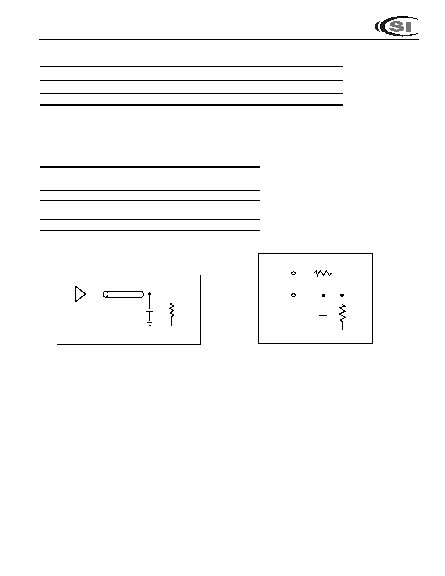
AC TEST CONDITIONS
Parameter
Unit
Input Pulse Level
0V to 3.0V
Input Rise and Fall Times
1.5 ns
Input and Output Timing
1.5V
and Reference Level
Output Load
See Figures 1 and 2
AC TEST LOADS
Output
Buffer
Z
O
= 50
1.5V
50
30 pF
Figure 2
317
5 pF
Including
jig and
scope
351
OUTPUT
3.3V
Figure 1
10
Integrated Circuit Solution Inc.
SSR019-0A
09/17/2001
IC61SP12832
IC61SP12836
READ/WRITE CYCLE SWITCHING CHARACTERISTICS
(Over Operating Range)
-
166
-150
-133
-117
-5
Symbol Parameter
Min.
Max.
Min.
Max.
Min.
Max.
Min.
Max.
Min.
Max.
Unit
f
MAX
Clock Frequency
--
166
--
150
--
133
--
117
--
100
MHz
t
KC
Cycle Time
6
--
6.7
--
7.5
--
8.5
--
10
--
ns
t
KH
Clock High Time
2.4
--
2.6
--
2.8
--
3.4
--
4
--
ns
t
KL
Clock Low Time
2.4
--
2.6
--
2.8
--
3.4
--
4
--
ns
t
KQ
Clock Access Time
--
3.5
--
3.8
--
4
--
4
--
5
ns
t
KQX
(1)
Clock High to Output Invalid
1.5
--
1.5
--
1.5
--
1.5
--
2.5
--
ns
t
KQLZ
(1,2)
Clock High to Output Low-Z
0
--
0
--
0
--
0
--
0
--
ns
t
KQHZ
(1,2)
Clock High to Output High-Z
1.5
6
1.5
6.7
1.5
7.5
1.5
8.5
1.5
10
ns
t
OEQ
Output Enable to Output Valid
--
3.5
--
3.5
--
3.8
--
4
--
5
ns
t
OEQX
(1)
Output Disable to Output Invalid
0
--
0
--
0
--
0
--
0
--
ns
t
OELZ
(1,2)
Output Enable to Output Low-Z
0
--
0
--
0
--
0
--
0
--
ns
t
OEHZ
(1,2)
Output Disable to Output High-Z
2
3.5
2
3.5
2
3.8
2
4
2
5
ns
t
AS
Address Setup Time
1.5
--
1.5
--
1.5
--
1.5
--
1.5
--
ns
t
SS
Address Status Setup Time
1.5
--
1.5
--
1.5
--
1.5
--
1.5
--
ns
t
WS
Write Setup Time
1.5
--
1.5
--
1.5
--
1.5
--
1.5
--
ns
t
CES
Chip Enable Setup Time
1.5
--
1.5
--
1.5
--
1.5
--
1.5
--
ns
t
AVS
Address Advance Setup Time
1.5
--
1.5
--
1.5
--
1.5
--
1.5
--
ns
t
AH
Address Hold Time
0.5
--
0.5
--
0.5
--
0.5
--
0.5
--
ns
t
SH
Address Status Hold Time
0.5
--
0.5
--
0.5
--
0.5
--
0.5
--
ns
t
WH
Write Hold Time
0.5
--
0.5
--
0.5
--
0.5
--
0.5
--
ns
t
CEH
Chip Enable Hold Time
0.5
--
0.5
--
0.5
--
0.5
--
0.5
--
ns
t
AVH
Address Advance Hold Time
0.5
--
0.5
--
0.5
--
0.5
--
0.5
--
ns
Note:
1. Guaranteed but not 100% tested. This parameter is periodically sampled.
2. Tested with load in Figure 2.
Integrated Circuit Solution Inc.
11
SSR019-0A
09/17/2001
IC61SP12832
IC61SP12836
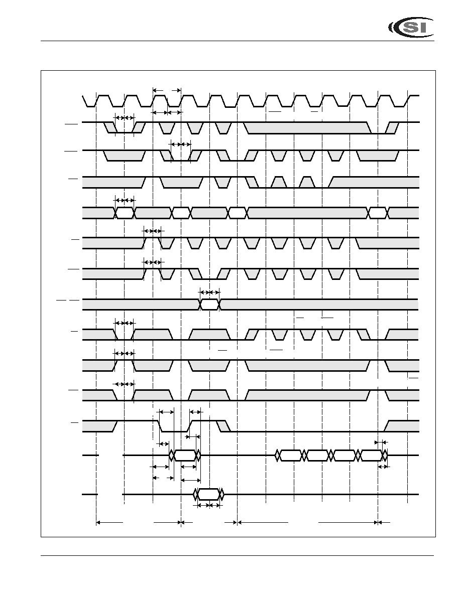
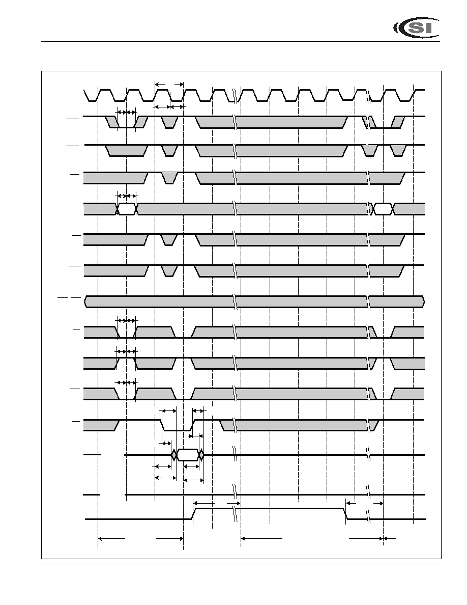
READ/WRITE CYCLE TIMING
Single Read
Single Write
High-Z
High-Z
DATA
OUT
DATA
IN
OE
CE2
CE2
CE
BW4-BW1
BWE
GW
A16-A0
ADV
ADSC
ADSP
CLK
RD1
WR1
WR1
1a
1a
2a
2b
2c
2d
Unselected
Burst Read
t
KQX
t
KC
t
KL
t
KH
t
SS
t
SH
ADSP is blocked by CE inactive
t
SS
t
SH
t
AS
t
AH
t
WS
t
WH
t
WS
t
WH
t
WS
t
WH
RD2
RD3
t
CES
t
CEH
t
CES
t
CEH
t
CES
t
CEH
CE2 and CE2 only sampled with ADSP or ADSC
CE Masks ADSP
Unselected with CE2
t
OEQ
t
OEQX
t
OELZ
t
KQLZ
t
KQ
t
OEHZ
t
KQX
t
KQHZ
t
DS
t
DH
t
KQHZ
12
Integrated Circuit Solution Inc.
SSR019-0A
09/17/2001
IC61SP12832
IC61SP12836
WRITE CYCLE SWITCHING CHARACTERISTICS
(Over Operating Range)
-
166
-150
-133
-117
-5
Symbol Parameter
Min.
Max.
Min.
Max.
Min.
Max.
Min.
Max.
Min.
Max.
Unit
t
KC
Cycle Time
6
--
6.7
--
7.5
--
8.5
--
10
--
ns
t
KH
Clock High Time
2.4
--
2.6
--
2.8
--
3.4
--
4
--
ns
t
KL
Clock Low Time
2.4
--
2.6
--
2.8
--
3.4
--
4
--
ns
t
AS
Address Setup Time
1.5
--
1.5
--
1.5
--
1.5
--
1.5
--
ns
t
SS
Address Status Setup Time
1.5
--
1.5
--
1.5
--
1.5
--
1.5
--
ns
t
WS
Write Setup Time
1.5
--
1.5
--
1.5
--
1.5
--
1.5
--
ns
t
DS
Data In Setup Time
1.5
--
1.5
--
1.5
--
1.5
--
1.5
--
ns
t
CES
Chip Enable Setup Time
1.5
--
1.5
--
1.5
--
1.5
--
1.5
--
ns
t
AVS
Address Advance Setup Time
1.5
--
1.5
--
1.5
--
1.5
--
1.5
--
ns
t
AH
Address Hold Time
0.5
--
0.5
--
0.5
--
0.5
--
0.5
--
ns
t
SH
Address Status Hold Time
0.5
--
0.5
--
0.5
--
0.5
--
0.5
--
ns
t
DH
Data In Hold Time
0.5
--
0.5
--
0.5
--
0.5
--
0.5
--
ns
t
WH
Write Hold Time
0.5
--
0.5
--
0.5
--
0.5
--
0.5
--
ns
t
CEH
Chip Enable Hold Time
0.5
--
0.5
--
0.5
--
0.5
--
0.5
--
ns
t
AVH
Address Advance Hold Time
0.5
--
0.5
--
0.5
--
0.5
--
0.5
--
ns
Integrated Circuit Solution Inc.
13
SSR019-0A
09/17/2001
IC61SP12832
IC61SP12836
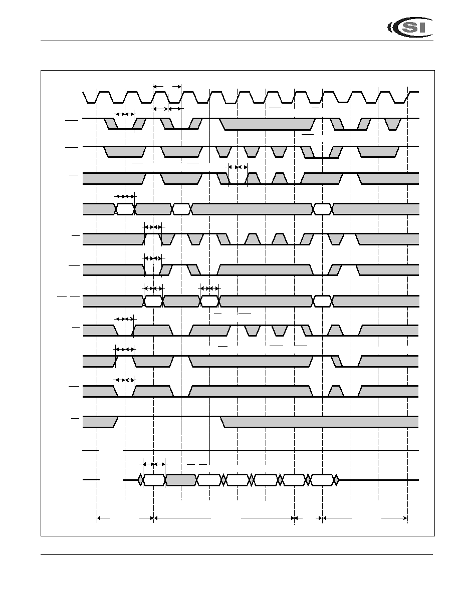
WRITE CYCLE TIMING
Single Write
DATA
OUT
DATA
IN
OE
CE2
CE2
CE
BW4-BW1
BWE
GW
A16-A0
ADV
ADSC
ADSP
CLK
WR1
WR2
Unselected
Burst Write
t
KC
t
KL
t
KH
t
SS
t
SH
t
AS
t
AH
t
WS
t
WH
t
WS
t
WH
WR3
t
CES
t
CEH
t
CES
t
CEH
t
CES
t
CEH
CE2 and CE2 only sampled with ADSP or ADSC
CE Masks ADSP
Unselected with CE2
ADSC initiate Write
ADSP is blocked by CE inactive
t
AVH
t
AVS
ADV must be inactive for ADSP Write
WR1
WR2
t
WS
t
WH
WR3
t
WS
t
WH
High-Z
High-Z
1a
3a
t
DS
t
DH
BW4-BW1 only are applied to first cycle of WR2
Write
2c
2d
2b
2a
14
Integrated Circuit Solution Inc.
SSR019-0A
09/17/2001
IC61SP12832
IC61SP12836
SNOOZE AND RECOVERY CYCLE SWITCHING CHARACTERISTICS
(Over Operating Range)
-
166
-150
-133
-117
-5
Symbol Parameter
Min.
Max.
Min.
Max.
Min.
Max.
Min.
Max.
Min.
Max.
Unit
t
KC
Cycle Time
6
--
6.7
--
7.5
--
8.5
--
10
--
ns
t
KH
Clock High Time
2.4
--
2.6
--
2.8
--
3.4
--
4
--
ns
t
KL
Clock Low Time
2.4
--
2.6
--
2.8
--
3.4
--
4
--
ns
t
KQ
Clock Access Time
--
3.5
--
3.8
--
4
--
4
--
5
ns
t
KQX
(1)
Clock High to Output Invalid
1.5
--
1.5
--
1.5
--
2
--
2.5
--
ns
t
KQLZ
(1,2)
Clock High to Output Low-Z
0
--
0
--
0
--
0
--
0
--
ns
t
KQHZ
(1,2)
Clock High to Output High-Z
1.5
3.6
1.5
6.7
1.5
7.5
1.5
8.5
1.5
10
ns
t
OEQ
Output Enable to Output Valid
--
3.5
--
3.5
--
3.9
--
4
--
5
ns
t
OEQX
(1)
Output Disable to Output Invalid
0
--
0
--
0
--
0
--
0
--
ns
t
OELZ
(1,2)
Output Enable to Output Low-Z
0
--
0
--
0
--
0
--
0
--
ns
t
OEHZ
(1,2)
Output Disable to Output High-Z
2
3.5
2
3.5
2
3.8
2
4
2
5
ns
t
AS
Address Setup Time
1.5
--
1.5
--
1.5
--
1.5
--
1.5
--
ns
t
SS
Address Status Setup Time
1.5
--
1.5
--
1.5
--
1.5
--
1.5
--
ns
t
CES
Chip Enable Setup Time
1.5
--
1.5
--
1.5
--
1.5
--
1.5
--
ns
t
AH
Address Hold Time
0.5
--
0.5
--
0.5
--
0.5
--
0.5
--
ns
t
SH
Address Status Hold Time
0.5
--
0.5
--
0.5
--
0.5
--
0.5
--
ns
t
CEH
Chip Enable Hold Time
0.5
--
0.5
--
0.5
--
0.5
--
0.5
--
ns
t
ZZS
ZZ Standby
2
--
2
--
2
--
2
--
2
--
cyc
t
ZZREC
ZZ Recovery
2
--
2
--
2
--
2
--
2
--
cyc
Notes:
1. Guaranteed but not 100% tested. This parameter is periodically sampled.
2. Tested with load in Figure 2.
Integrated Circuit Solution Inc.
15
SSR019-0A
09/17/2001
IC61SP12832
IC61SP12836
SNOOZE AND RECOVERY CYCLE TIMING
Single Read
High-Z
High-Z
DATA
OUT
DATA
IN
ZZ
OE
CE2
CE2
CE
BW4-BW1
BWE
GW
A16-A0
ADV
ADSC
ADSP
CLK
RD1
1a
Read
Snooze with Data Retention
t
KC
t
KL
t
KH
t
SS
t
SH
t
AS
t
AH
RD2
t
CES
t
CEH
t
CES
t
CEH
t
CES
t
CEH
t
OEQ
t
OEQX
t
OELZ
t
KQLZ
t
KQ
t
OEHZ
t
KQX
t
KQHZ
t
ZZS
t
ZZREC
16
Integrated Circuit Solution Inc.
SSR019-0A
09/17/2001
IC61SP12832
IC61SP12836
ORDERING INFORMATION
Commercial Range: 0�C to +70�C
Speed
Order Part Number
Package
166 MHz
IC61SP12832-166TQ
14x20x1.4mm LQFP
IC61SP12832-166B
14*22mm PBGA
150 MHz
IC61SP12832-150TQ
14*20*1.4mm LQFP
IC61SP12832-150B
14*22mm PBGA
133 MHz
IC61SP12832-133TQ
14*20*1.4mm LQFP
IC61SP12832-133B
14*22mm PBGA
117 MHz
IC61SP12832-117TQ
14*20*1.4mm LQFP
IC61SP12832-117B
14*22mm PBGA
100 MHz
IC61SP12832-5TQ
14*20*1.4mm LQFP
IC61SP12832-5B
14*22mm PBGA
Speed
Order Part Number
Package
166 MHz
IC61SP12836-166TQ
14x20x1.4mm LQFP
IC61SP12836-166B
14*22mm PBGA
150 MHz
IC61SP12836-150TQ
14*20*1.4mm LQFP
IC61SP12836-150B
14*22mm PBGA
133 MHz
IC61SP12836-133TQ
14*20*1.4mm LQFP
IC61SP12836-133B
14*22mm PBGA
117 MHz
IC61SP12836-117TQ
14*20*1.4mm LQFP
IC61SP12836-117B
14*22mm PBGA
100 MHz
IC61SP12836-5TQ
14*20*1.4mm LQFP
IC61SP12836-5B
14*22mm PBGA
Integrated Circuit Solution Inc.
HEADQUARTER:
NO.2, TECHNOLOGY RD. V, SCIENCE-BASED INDUSTRIAL PARK,
HSIN-CHU, TAIWAN, R.O.C.
TEL: 886-3-5780333
Fax: 886-3-5783000
BRANCH OFFICE:
7F, NO. 106, SEC. 1, HSIN-TAI 5
TH
ROAD,
HSICHIH TAIPEI COUNTY, TAIWAN, R.O.C.
TEL: 886-2-26962140
FAX: 886-2-26962252
http://www.icsi.com.tw