
IC63LV1024
Integrated Circuit Solution Inc.
1
AHSR025-0D
04/16/2004
Document Title
128K x 8 Hight Speed SRAM with 3.3V Central Power
Revision History
Revision No
History
Draft Date
Remark
0A
Initial Draft
September 12,2001
0B
Add B (36-pin TF-BGA 6x8mm)
June 20,2002
and H (32-pin TSOP-1 8x13.4mm)
package type
0C
To correct the TYPO error
October 16,2003
0D
Obsolete "H" type
April 16,2004
The attached datasheets are provided by ICSI. Integrated Circuit Solution Inc reserve the right to change the specifications and
products. ICSI will answer to your questions about device. If you have any questions, please contact the ICSI offices.
IC63LV1024
2
Integrated Circuit Solution Inc.
AHSR025-0D
04/16/2004
ICSI reserves the right to make changes to its products at any time without notice in order to improve design and supply the best possible product. We assume no responsibility for any errors
which may appear in this publication. � Copyright 2000, Integrated Circuit Solution Inc.
128K x 8 HIGH-SPEED CMOS STATIC RAM
3.3V REVOLUTIONARY PINOUT
FEATURES
� High-speed access times:
8, 10, 12 and 15 ns
� High-performance, low-power CMOS process
� Multiple center power and ground pins for
greater noise immunity
� Easy memory expansion with CE and OE
options
� CE power-down
� Fully static operation: no clock or refresh
required
� TTL compatible inputs and outputs
� Single 3.3V power supply
� Packages available:
� 32-pin 300mil SOJ
� 32-pin 400mil SOJ
� 32-pin 400mil TSOP-2
� 36-pin TF-BGA (6mmx8mm)
DESCRIPTION
The
ICSI
IC63LV1024 is a very high-speed, low power, 131,
072-word by 8-bit CMOS static RAM in revolutionary pinout.
The IC63LV1024 is fabricated using
ICSI
's high-perform-
ance CMOS technology. This highly reliable process coupled
with innovative circuit design techniques, yields higher
performance and low power consumption devices.
When CE is HIGH (deselected), the device assumes a
standby mode at which the power dissipation can be
reduced down to 250 �W (typical) with CMOS input levels.
The IS63LV1024 operates from a single 3.3V power supply
and all inputs are TTL-compatible.
The IS63LV1024 is available in 32-pin 300mil SOJ, 400mil
SOJ, 400mil TSOP-2 and 36-pin TF-BGA (6mmx8mm).
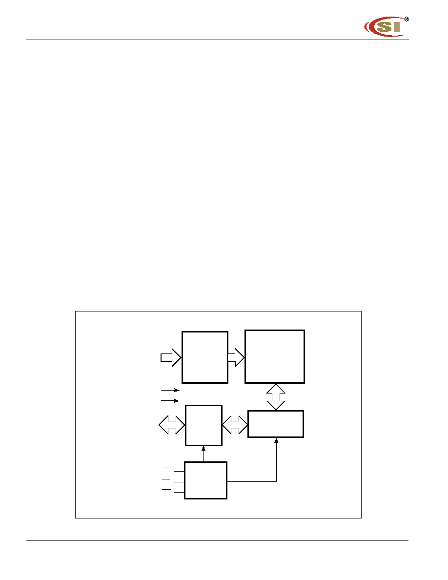
FUNCTIONAL BLOCK DIAGRAM
A0-A16
CE
OE
WE
128K X 8
MEMORY ARRAY
DECODER
COLUMN I/O
CONTROL
CIRCUIT
GND
VCC
I/O
DATA
CIRCUIT
I/O0-I/O7
IC63LV1024
Integrated Circuit Solution Inc.
3
AHSR025-0D
04/16/2004
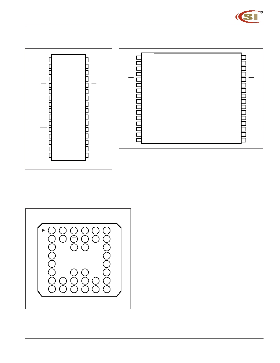
PIN CONFIGURATION
32-Pin SOJ
1
2
3
4
5
6
7
8
9
10
11
12
13
14
15
16
32
31
30
29
28
27
26
25
24
23
22
21
20
19
18
17
A0
A1
A2
A3
CE
I/O0
I/O1
Vcc
GND
I/O2
I/O3
WE
A4
A5
A6
A7
A16
A15
A14
A13
OE
I/O7
I/O6
GND
Vcc
I/O5
I/O4
A12
A11
A10
A9
A8
1
2
3
4
5
6
7
8
9
10
11
12
13
14
15
16
32
31
30
29
28
27
26
25
24
23
22
21
20
19
18
17
A0
A1
A2
A3
CE
I/O0
I/O1
Vcc
GND
I/O2
I/O3
WE
A4
A5
A6
A7
A16
A15
A14
A13
OE
I/O7
I/O6
GND
Vcc
I/O5
I/O4
A12
A11
A10
A9
A8
PIN CONFIGURATION
32-Pin TSOP-2
PIN CONFIGURATION
36-Pin TF-BGA (TOP View)
(6mm x 8mm)
1 2 3 4 5 6
A
B
C
D
E
F
G
H
A0
A1
NC
A3
A6
A8
I/O
4
A2
WE
A4
A7
I/O
0
I/O
5
NC
A5
I/O
1
GND
Vcc
Vcc
GND
I/O
6
NC
NC
I/O
2
I/O
7
CE
A16
A15
I/O
3
A9
A10
A11
A12
A13
A14
OE
IC63LV1024
4
Integrated Circuit Solution Inc.
AHSR025-0D
04/16/2004
PIN DESCRIPTIONS
A0-A16
Address Inputs
CE
Chip Enable Input
OE
Output Enable Input
WE
Write Enable Input
I/O1-I/O8
Bidirectional Ports
Vcc
Power
GND
Ground
ABSOLUTE MAXIMUM RATINGS
(1)
Symbol
Parameter
Value
Unit
V
TERM
Terminal Voltage with Respect to GND
�0.5 to Vcc + 0.5
V
T
BIAS
Temperature Under Bias
�55 to +125
�C
T
STG
Storage Temperature
�65 to +150
�C
P
T
Power Dissipation
1.0
W
Notes:
1. Stress greater than those listed under ABSOLUTE MAXIMUM RATINGS may cause
permanent damage to the device. This is a stress rating only and functional operation of the
device at these or any other conditions above those indicated in the operational sections of
this specification is not implied. Exposure to absolute maximum rating conditions for
extended periods may affect reliability.
TRUTH TABLE
Mode
WE
WE
WE
WE
WE
CE
CE
CE
CE
CE
OE
OE
OE
OE
OE
I/O Operation Vcc Current
Not Selected
X
H
X
High-Z
I
SB
1
, I
SB
2
(Power-down)
Output Disabled H
L
H
High-Z
I
CC
1
, I
CC
2
Read
H
L
L
D
OUT
I
CC
1
, I
CC
2
Write
L
L
X
D
IN
I
CC
1
, I
CC
2
IC63LV1024
Integrated Circuit Solution Inc.
5
AHSR025-0D
04/16/2004
DC ELECTRICAL CHARACTERISTICS
(Over Operating Range)
Symbol Parameter
Test Conditions
Min.
Max.
Unit
V
OH
Output HIGH Voltage
V
CC
= Min., I
OH
= �4.0 mA
2.4
--
V
V
OL
Output LOW Voltage
V
CC
= Min., I
OL
= 8.0 mA
--
0.4
V
V
IH
Input HIGH Voltage
2.2
V
CC
+ 0.3
V
V
IL
Input LOW Voltage
(1)
�0.3
0.8
V
I
LI
Input Leakage
GND
V
IN
V
CC
Com.
�2
2
�A
Ind.
�5
5
I
LO
Output Leakage
GND
V
OUT
V
CC
, Outputs Disabled
Com.
�2
2
�A
Ind.
�5
5
Notes:
1. V
IL
= �3.0V for pulse width less than 10 ns.
2. The Vcc operating range for 8 ns is 3.3V +10%, -5%.
CAPACITANCE
(1,2)
Symbol
Parameter
Conditions
Max.
Unit
C
IN
Input Capacitance
V
IN
= 0V
6
pF
C
I/O
Input/Output Capacitance
V
OUT
= 0V
8
pF
Notes:
1. Tested initially and after any design or process changes that may affect these parameters.
2. Test conditions: T
A
= 25�C, f = 1 MHz, Vcc = 3.3V.
POWER SUPPLY CHARACTERISTICS
(1)
(Over Operating Range)
-8 ns
-10 ns
-12 ns
-15 ns
Symbol Parameter
Test Conditions
Min.
Max.
Min.
Max.
Min.
Max.
Min.
Max. Unit
I
CC
1
Vcc Operating
V
CC
= Max., CE = V
IL
Com.
--
160
--
150
--
140
--
130
mA
Supply Current
I
OUT
= 0 mA, f = Max.
Ind.
--
170
--
160
--
150
--
140
I
SB
1
TTL Standby
V
CC
= Max.,
Com.
--
30
--
30
--
30
--
30
mA
Current
V
IN
= V
IH
or V
IL
Ind.
--
40
--
40
--
40
--
40
(TTL Inputs)
CE
V
IH
, f = 0
I
SB
2
CMOS Standby
V
CC
= Max.,
Com.
--
10
--
10
--
10
--
10
mA
Current
CE
V
CC
� 0.2V,
Ind.
--
15
--
15
--
15
--
15
(CMOS Inputs)
V
IN
V
CC
� 0.2V, or
V
IN
0.2V, f = 0
Notes:
1. At f = f
MAX
, address and data inputs are cycling at the maximum frequency, f = 0 means no input lines change.
OPERATING RANGE
Range
Ambient Temperature
V
CC
Commercial
0�C to +70�C
3.3V
�
0.3V
Industrial
�40�C to +85�C
3.3V
�
0.3V
IC63LV1024
6
Integrated Circuit Solution Inc.
AHSR025-0D
04/16/2004
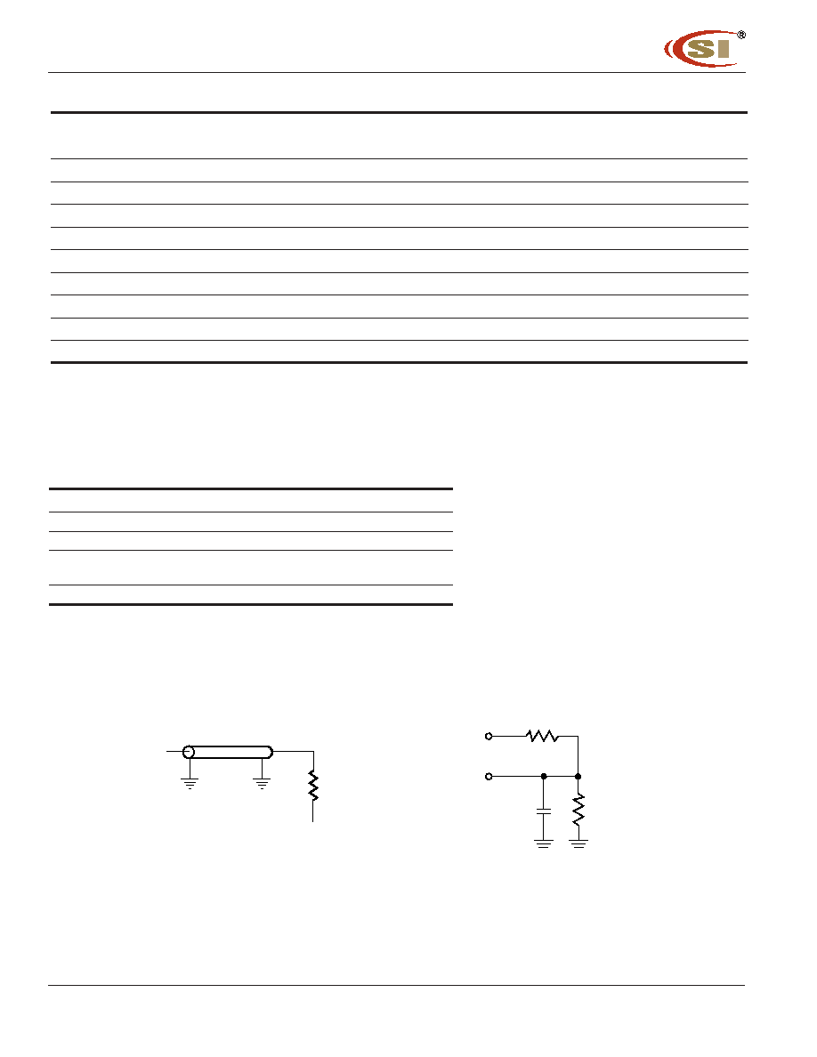
AC TEST LOADS
AC TEST CONDITIONS
Parameter
Unit
Input Pulse Level
0V to 3.0V
Input Rise and Fall Times
3 ns
Input and Output Timing
1.5V
and Reference Levels
Output Load
See Figures 1a and 1b
Notes:
1. The Vcc operating range for 8 ns is 3.3V +10%, -5%.
READ CYCLE SWITCHING CHARACTERISTICS
(1)
(Over Operating Range)
-8 ns
-10 ns
-12 ns
-15 ns
Symbol
Parameter
Min.
Max.
Min.
Max.
Min.
Max.
Min.
Max.
Unit
t
RC
Read Cycle Time
8
--
10
--
12
--
15
--
ns
t
AA
Address Access Time
--
8
--
10
--
12
--
15
ns
t
OHA
Output Hold Time
3
--
3
--
3
--
3
--
ns
t
ACE
CE Access Time
--
8
--
10
--
12
--
15
ns
t
DOE
OE Access Time
--
4
--
5
--
6
--
7
ns
t
LZOE
(2)
OE to Low-Z Output
0
--
0
--
0
--
0
--
ns
t
HZOE
(2)
OE to High-Z Output
0
4
0
5
0
6
0
7
ns
t
LZCE
(2)
CE to Low-Z Output
3
--
3
--
3
--
3
--
ns
t
HZCE
(2)
CE to High-Z Output
0
4
0
5
0
6
0
7
ns
Notes:
1. Test conditions assume signal transition times of 3 ns or less, timing reference levels of 1.5V, input pulse levels of 0 to 3.0V
and output loading specified in Figure 1a.
2. Tested with the load in Figure 1b. Transition is measured
�
500 mV from steady-state voltage. Not 100% tested.
OUTPUT
V
T
= 1.5V
Z
OUT
= 50
50
317
5 pF
Including
jig and
scope
351
OUTPUT
3.3V
Figure 1a.
Figure 1b.
IC63LV1024
Integrated Circuit Solution Inc.
7
AHSR025-0D
04/16/2004
DATA VALID
READ1.eps
PREVIOUS DATA VALID
t
AA
t
OHA
t
OHA
t
RC
D
OUT
ADDRESS
t
RC
t
OHA
t
AA
t
DOE
t
LZOE
t
ACE
t
LZCE
t
HZOE
HIGH-Z
DATA VALID
CE_RD2.eps
ADDRESS
OE
CE
D
OUT
t
HZCE
READ CYCLE NO. 2
(1,3)
Notes:
1. WE is HIGH for a Read Cycle.
2. The device is continuously selected. OE, CE = V
IL
.
3. Address is valid prior to or coincident with CE LOW transitions.
AC WAVEFORMS
READ CYCLE NO. 1
(1,2)
IC63LV1024
8
Integrated Circuit Solution Inc.
AHSR025-0D
04/16/2004
WRITE CYCLE SWITCHING CHARACTERISTICS
(1,3)
(Over Operating Range)
-8 ns
-10 ns
-12 ns
-15 ns
Symbol Parameter
Min.
Max.
Min.
Max.
Min.
Max.
Min.
Max.
Unit
t
WC
Write Cycle Time
8
--
10
--
12
--
15
--
ns
t
SCE
CE to Write End
7
--
8
--
9
--
10
--
ns
t
AW
Address Setup Time to
7
--
8
--
9
--
10
--
ns
Write End
t
HA
Address Hold from
0
--
0
--
0
--
0
--
ns
Write End
t
SA
Address Setup Time
0
--
0
--
0
--
0
--
ns
t
PWE
(4)
WE Pulse Width
7
--
8
--
9
--
10
--
ns
t
SD
Data Setup to Write End
4.5
--
6
--
6
--
7
--
ns
t
HD
Data Hold from Write End
0
--
0
--
0
--
0
--
ns
t
HZWE
(2)
WE LOW to High-Z Output
0
4
0
5
0
6
0
7
ns
t
LZWE
(2)
WE HIGH to Low-Z Output
0
--
0
--
0
--
0
--
ns
Notes:
1. Test conditions assume signal transition times of 3ns or less, timing reference levels of 1.5V, input pulse levels of 0 to 3.0V and
output loading specified in Figure 1a.
2. Tested with the load in Figure 1b. Transition is measured �500 mV from steady-state voltage. Not 100% tested.
3. The internal write time is defined by the overlap of CE LOW and WE LOW. All signals must be in valid states to initiate a Write,
but any one can go inactive to terminate the Write. The Data Input Setup and Hold timing are referenced to the rising or falling
edge of the signal that terminates the Write.
4. Tested with OE HIGH.
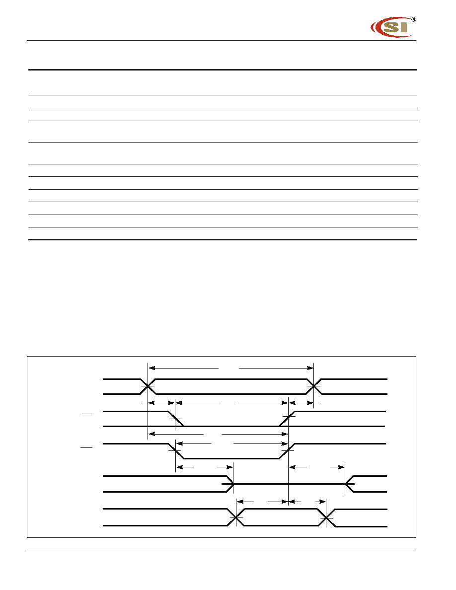
AC WAVEFORMS
WRITE CYCLE NO. 1
(WE Controlled)
(1,2)
DATA UNDEFINED
t
WC
VALID ADDRESS
t
SCE
t
PWE1
t
PWE2
t
AW
t
HA
HIGH-Z
t
HD
t
SA
t
HZWE
ADDRESS
CE
WE
D
OUT
D
IN
DATA
IN
VALID
t
LZWE
t
SD
CE_WR1.eps
IC63LV1024
Integrated Circuit Solution Inc.
9
AHSR025-0D
04/16/2004
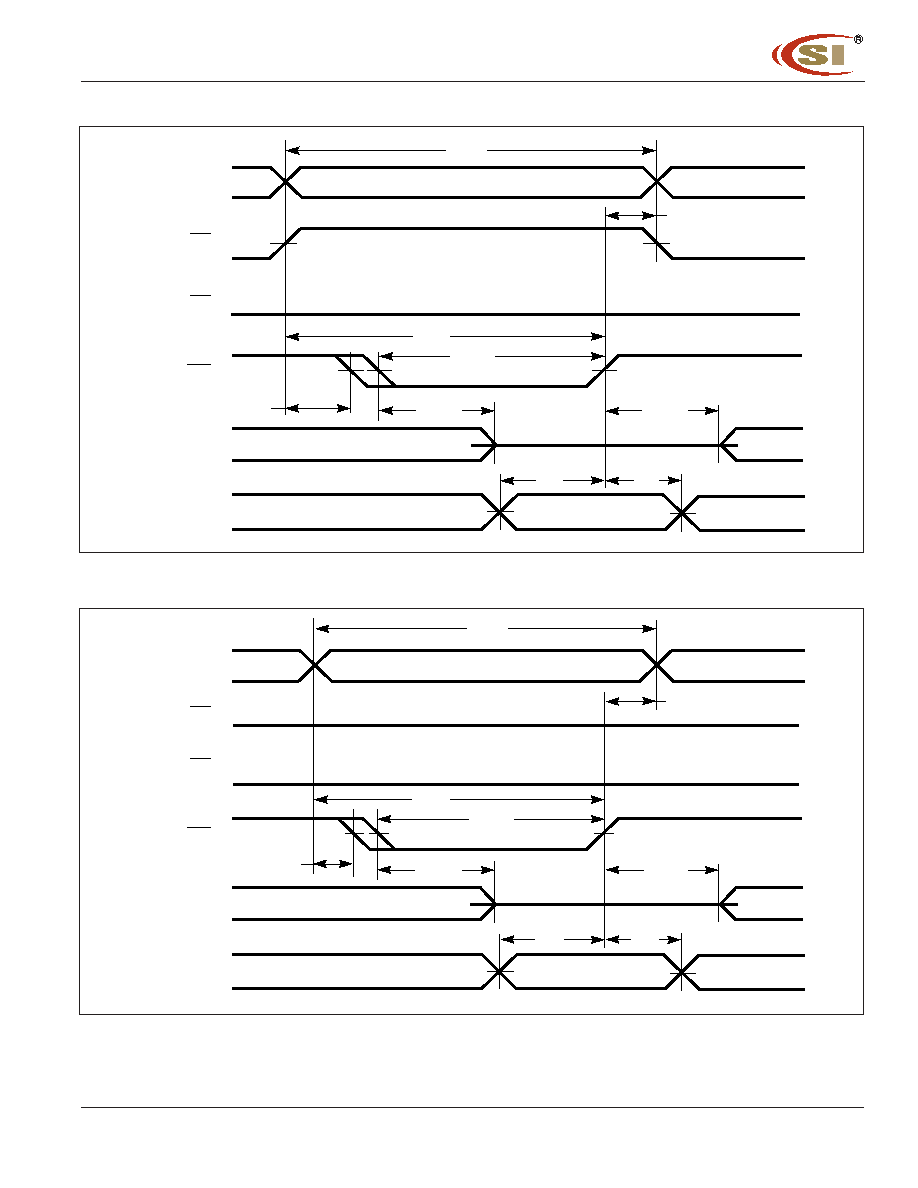
DATA UNDEFINED
LOW
t
WC
VALID ADDRESS
t
PWE1
t
AW
t
HA
HIGH-Z
t
HD
t
SA
t
HZWE
ADDRESS
CE
WE
D
OUT
D
IN
OE
DATA
IN
VALID
t
LZWE
t
SD
CE_WR2.eps
WRITE CYCLE NO. 2
(CE Controlled)
(1,2)
WRITE CYCLE NO. 3
(WE Controlled: OE is LOW During Write Cycle)
DATA UNDEFINED
t
WC
VALID ADDRESS
LOW
LOW
t
PWE2
t
AW
t
HA
HIGH-Z
t
HD
t
SA
t
HZWE
ADDRESS
CE
WE
D
OUT
D
IN
OE
DATA
IN
VALID
t
LZWE
t
SD
CE_WR3.eps
Notes:
1. The internal write time is defined by the overlap of CE LOW and WE LOW. All signals must be in valid states to initiate a Write,
but any one can go inactive to terminate the Write. The Data Input Setup and Hold timing are referenced to the rising or falling
edge of the signal that terminates the Write.
2. I/O will assume the High-Z state if OE
V
IH
.
IC63LV1024
10
Integrated Circuit Solution Inc.
AHSR025-0D
04/16/2004
ORDERING INFORMATION
Commercial Range: 0�C to +70�C
Speed (ns)
Order Part No.
Package
8
IC63LV1024-8B
6*8mm TF-BGA
8
IC63LV1024-8T
400mil T SOP-2
8
IC63LV1024-8J
300mil SOJ
8
IC63LV1024-8K
400mil SOJ
10
IC63LV1024-10B
6*8mm TF-BGA
10
IC63LV1024-10T
400mil T SOP-2
10
IC63LV1024-10J
300mil SOJ
10
IC63LV1024-10K
400mil SOJ
12
IC63LV1024-12B
6*8mm TF-BGA
12
IC63LV1024-12T
400mil T SOP-2
12
IC63LV1024-12J
300mil SOJ
12
IC63LV1024-12K
400mil SOJ
15
IC63LV1024-15B
6*8mm TF-BGA
15
IC63LV1024-15T
400mil T SOP-2
15
IC63LV1024-15J
300mil SOJ
15
IC63LV1024-15K
400mil SOJ
ORDERING INFORMATION
Industrial Range: �40�C to +85�C
Speed (ns)
Order Part No.
Package
8
IC63LV1024-8BI
6*8mm TF-BGA
8
IC63LV1024-8TI
400mil T SOP-2
8
IC63LV1024-8JI
300mil SOJ
8
IC63LV1024-8KI
400mil SOJ
10
IC63LV1024-10BI
6*8mm TF-BGA
10
IC63LV1024-10TI
400mil T SOP-2
10
IC63LV1024-10JI
300mil SOJ
10
IC63LV1024-10KI
400mil SOJ
12
IC63LV1024-12BI
6*8mm TF-BGA
12
IC63LV1024-12TI
400mil T SOP-2
12
IC63LV1024-12JI
300mil SOJ
12
IC63LV1024-12KI
400mil SOJ
15
IC63LV1024-15BI
6*8mm TF-BGA
15
IC63LV1024-15TI
400mil T SOP-2
15
IC63LV1024-15JI
300mil SOJ
15
IC63LV1024-15KI
400mil SOJ
Integrated Circuit Solution Inc.
HEADQUARTER:
NO.2, TECHNOLOGY RD. V, SCIENCE-BASED INDUSTRIAL PARK,
HSIN-CHU, TAIWAN, R.O.C.
TEL: 886-3-5780333
Fax: 886-3-5783000
BRANCH OFFICE:
7F, NO. 106, SEC. 1, HSIN-TAI 5
TH
ROAD,
HSICHIH TAIPEI COUNTY, TAIWAN, R.O.C.
TEL: 886-2-26962140
FAX: 886-2-26962252
http://www.icsi.com.tw