
Integrated Circuit Solution Inc.
1
MC002-0B
IC80C52
IC80C32
ICSI reserves the right to make changes to its products at any time without notice in order to improve design and supply the best possible product. We assume no responsibility for any errors
which may appear in this publication. © Copyright 2000, Integrated Circuit Solution Inc.
IC80C52
IC80C32
CMOS SINGLE CHIP
8-BIT MICROCONTROLLER
FEATURES
∑ 80C52 based architecture
∑ 8K x 8 ROM (IC80C52 only)
∑ 256 x 8 RAM
∑ Three 16-bit Timer/Counters
∑ Full duplex serial channel
∑ Boolean processor
∑ Four 8-bit I/O ports, 32 I/O lines
∑ Memory addressing capability
≠ 64K ROM and 64K RAM
∑ Program memory lock
≠ Encrypted verify (32 bytes)
≠ Lock bits (2)
∑ Power save modes:
≠ Idle and power-down
∑ Eight interrupt sources
∑ Most instructions execute in 0.3 µs
∑ CMOS and TTL compatible
∑ Maximum speed: 40 MHz @ Vcc = 5V
∑ Packages available:
≠ 40-pin DIP
≠ 44-pin PLCC
≠ 44-pin PQFP
GENERAL DESCRIPTION
The
ICSI
IC80C52 and IC80C32 are high-performance
microcontroller fabricated using high-density CMOS
technology. The CMOS IC80C52/32 is functionally
compatible with is the industry standard 80C52/32
microcontrollers.
The IC80C52/32 is designed with 8K x 8 ROM (IC80C52
only); 256 x 8 RAM; 32 programmable I/O lines; a serial I/
O port for either multiprocessor communications, I/O
expansion or full duplex UART; three 16-bit timer/counters;
an eight-source, two-priority-level, nested interrupt
structure; and an on-chip oscillator and clock circuit. The
IC80C52/32 can be expanded using standard TTL
compatible memory.
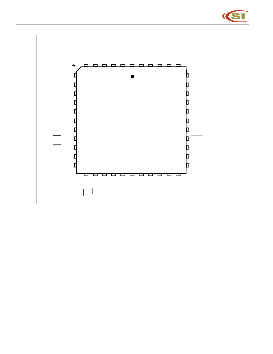
Figure 1. IC80C52/32 Pin Configuration: 40-pin DIP
1
2
3
4
5
6
7
8
9
10
11
12
13
14
15
16
17
18
19
20
40
39
38
37
36
35
34
33
32
31
30
29
28
27
26
25
24
23
22
21
T2/P1.0
T2EX/P1.1
P1.2
P1.3
P1.4
P1.5
P1.6
P1.7
RST
RxD/P3.0
TxD/P3.1
INT0/P3.2
INT1/P3.3
T0/P3.4
T1/P3.5
WR/P3.6
RD/P3.7
XTAL2
XTAL1
GND
V
CC
P0.0/AD0
P0.1/AD1
P0.2/AD2
P0.3/AD3
P0.4/AD4
P0.5/AD5
P0.6/AD6
P0.7/AD7
EA
ALE
PSEN
P2.7/A15
P2.6/A14
P2.5/A13
P2.4/A12
P2.3/A11
P2.2/A10
P2.1/A9
P2.0/A8
IC80C52
IC80C32
2
Integrated Circuit Solution Inc.
MC002-0B
TOP VIEW
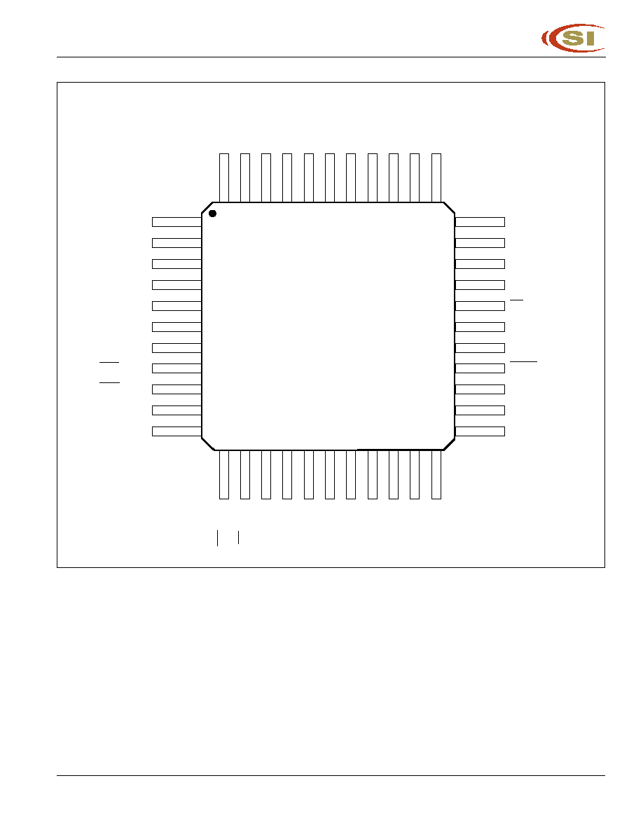
Figure 2. IC80C52/32 Pin Configuration: 44-pin PLCC
WR/P3.6
RD/P3.7
XTAL2
XTAL1
GND
NC
A8/P2.0
A9/P2.1
A10/P2.2
A11/P2.3
A12/P2.4
P1.4
P1.3
P1.2
P1.1/T2EX
P1.0/T2
NC
V
CC
P0.0/AD0
P0.1/AD1
P0.2/AD2
P0.3/AD3
P0.4/AD4
P0.5/AD5
P0.6/AD6
P0.7/AD7
EA
NC
ALE
PSEN
P2.7/A15
P2.6/A14
P2.5/A13
P1.5
P1.6
P1.7
RST
RxD/P3.0
NC
TxD/P3.1
INT0/P3.2
INT1/P3.3
T0/P3.4
T1/P3.5
7
8
9
10
11
12
13
14
15
16
17
39
38
37
36
35
34
33
32
31
30
29
INDEX
4
3
6
5
2
1
44
18
19
20
21
22
23
24
43
42
41
40
25
26
27
28
Integrated Circuit Solution Inc.
3
MC002-0B
IC80C52
IC80C32
Figure 3. IC80C52/32 Pin Configuration: 44-pin PQFP
WR/P3.6
RD/P3.7
XTAL2
XTAL1
GND
NC
A8/P2.0
A9/P2.1
A10/P2.2
A11/P2.3
A12/P2.4
P1.4
P1.3
P1.2
P1.1/T2EX
P1.0/T2
NC
V
CC
P0.0/AD0
P0.1/AD1
P0.2/AD2
P0.3/AD3
P0.4/AD4
P0.5/AD5
P0.6/AD6
P0.7/AD7
EA
NC
ALE
PSEN
P2.7/A15
P2.6/A14
P2.5/A13
P1.5
P1.6
P1.7
RST
RxD/P3.0
NC
TxD/P3.1
INT0/P3.2
INT1/P3.3
T0/P3.4
T1/P3.5
1
2
3
4
5
6
7
8
9
10
11
33
32
31
30
29
28
27
26
25
24
23
38
12
13
14
15
16
17
18
37
36
35
34
44
43
42
41
40
39
19
20
21
22
IC80C52
IC80C32
4
Integrated Circuit Solution Inc.
MC002-0B
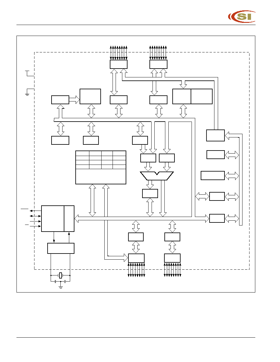
Figure 4. IC80C52/32 Block Diagram
PCON
SCON
TMOD
TCON
T2CON
TH0
TL0
TH1
TL1
TH2
TL2
RCAP2H
RCAP2L SBUF
IE
IP
INTERRUPT
SERIAL PORT
AND TIMER BLOCK
P3
DRIVERS
P3
LATCH
PSW
TIMING
AND
CONTROL
OSCILLATOR
XTAL2
XTAL1
INSTRUCTION
REGISTER
P3.0-P3.7
P1
DRIVERS
P1
LATCH
DPTR
BUFFER
PC
INCREMENTER
PROGRAM
COUNTER
PROGRAM
ADDRESS
REGISTER
P1.0-P1.7
P2.0-P2.7
P0.0-P0.7
PSEN
ALE
RST
EA
TMP2
ALU
ACC
STACK
POINT
B
REGISTER
V
CC
GND
RAM ADDR
REGISTER
P2
LATCH
P0
LATCH
P2
DRIVERS
P0
DRIVERS
ADDRESS
DECODER
& 256
BYTES RAM
ADDRESS
DECODER
&
8K ROM
2 LOCK BITS
&
32 BYTES
ENCRYPTION
TMP1

Integrated Circuit Solution Inc.
5
MC002-0B
IC80C52
IC80C32
Table 1. Detailed Pin Description
Symbol
PDIP
PLCC
PQFP
I/O
Name and Function
ALE
30
33
27
I/O
Address Latch Enable: Output pulse for latching the low byte
of the address during an access to the external memory. In
normal operation, ALE is emitted at a constant rate of 1/6 the
oscillator frequency, and can be used for external timing or
clocking. Note that one ALE pulse is skipped during each
access to external data memory.
EA
31
35
29
I
External Access enable:
EA must be externally held low to
enable the device to fetch code from external program memory
locations 0000H to FFFFH. If
EA is held high, the device
executes from internal program memory unless the program
counter contains an address greater than internal ROM size.
P0.0-P0.7
39-32
43-36
37-30
I/O
Port 0: Port 0 is an 8-bit open-drain, bidirectional I/O port. Port
0 pins that have 1s written to them float and can be used as high-
impedance inputs. Port 0 is also the multiplexed low-order
address and data bus during accesses to external program and
data memory. In this application, it uses strong internal pullups
when emitting 1s.
P1.0-P1.7
1-8
2-9
40-44
I/O
Port 1: Port 1 is an 8-bit bidirectional I/O port with internal
1-3
pullups. Port 1 pins that have 1s written to them are pulled high
by the internal pullups and can be used as inputs. As inputs, Port
1 pins that are externally pulled low will source current because
of the internal pullups. (See DC Characteristics: I
IL
). The Port 1
output buffers can sink/source four TTL inputs.
Port 1 also receives the low-order address byte during Flash
programming and verification.
1
2
40
I
T2(P1.0): Timer/Counter 2 external count input.
2
3
41
I
T2EX(P1.1): Timer/Counter 2 trigger input.
P2.0-P2.7
21-28
24-31
18-25
I/O
Port 2: Port 2 is an 8-bit bidirectional I/O port with internal
pullups. Port 2 pins that have 1s written to them are pulled high
by the internal pullups and can be used as inputs. As inputs, Port
2 pins that are externally pulled low will source current because
of the internal pullups. (See DC Characteristics: I
IL
). Port 2 emits
the high order address byte during fetches from external pro-
gram memory and during accesses to external data memory
that used 16-bit addresses (MOVX @ DPTR). In this application,
Port 2 uses strong internal pullups when emitting 1s. During
accesses to external data memory that use 8-bit addresses
(MOVX @ Ri [i = 0, 1]), Port 2 emits the contents of the P2
Special Function Register.
Port 2 also receives the high-order bits and some control signals
during Flash programming and verification. P2.6 and P2.7 are
the control signals while the chip programs and erases.

IC80C52
IC80C32
6
Integrated Circuit Solution Inc.
MC002-0B
Symbol
PDIP
PLCC
PQFP
I/O
Name and Function
P3.0-P3.7
10-17
11, 13-19
5, 7-13
I/O
Port 3: Port 3 is an 8-bit bidirectional I/O port with internal
pullups. Port 3 pins that have 1s written to them are pulled high
by the internal pullups and can be used as inputs. As inputs, Port
3 pins that are externally pulled low will source current because
of the internal pullups. (See DC Characteristics: I
IL
).
Port 3 also serves the special features of the IC80C52, as listed
below:
10
11
5
I
RxD (P3.0): Serial input port.
11
13
7
O
TxD (P3.1): Serial output port.
12
14
8
I
INT0
INT0
INT0
INT0
INT0 (P3.2): External interrupt 0.
13
15
9
I
INT1
INT1
INT1
INT1
INT1 (P3.3): External interrupt 1.
14
16
10
I
T0 (P3.4): Timer 0 external input.
15
17
11
I
T1 (P3.5): Timer 1 external input.
16
18
12
O
WR
WR
WR
WR
WR (P3.6): External data memory write strobe.
17
19
13
O
RD
RD
RD
RD
RD (P3.7): External data memory read strobe.
PSEN
29
32
26
O
Program Store Enable: The read strobe to external program
memory. When the device is executing code from the external
program memory,
PSEN is activated twice each machine cycle
except that two
PSEN activations are skipped during each
access to external data memory.
PSEN is not activated during
fetches from internal program memory.
RST
9
10
4
I
Reset: A high on this pin for two machine cycles while the
oscillator is running, resets the device. An internal MOS resistor
to GND permits a power-on reset using only an external capaci-
tor connected to Vcc.
XTAL 1
19
21
15
I
Crystal 1: Input to the inverting oscillator amplifier and input
to the internal clock generator circuits.
XTAL 2
18
20
14
O
Crystal 2: Output from the inverting oscillator amplifier.
GND
20
22
16
I
Ground: 0V reference.
Vcc
40
44
38
I
Power Supply: This is the power supply voltage for operation.
Table 1. Detailed Pin Description (continued)

Integrated Circuit Solution Inc.
7
MC002-0B
IC80C52
IC80C32
OPERATING DESCRIPTION
The detail description of the IC80C52 included in this
description are:
∑ Memory Map and Registers
∑ Timer/Counters
∑ Serial Interface
∑ Interrupt System
∑ Other Information
∑ Flash Memory
MEMORY MAP AND REGISTERS
Memory
The IC80C52/32 has separate address spaces for program
and data memory. The program and data memory can be
up to 64K bytes long. The lower 8K program memory can
reside on-chip.(IC80C52 only) Figure 5 shows a map of the
IC80C52/32 program and data memory.
The IC80C52/32 has 256 bytes of on-chip RAM, plus
numbers of special function registers. The lower 128 bytes
can be accessed either by direct addressing or by indirect
addressing. Figure 6 shows internal data memory
organization and SFR Memory Map.
The lower 128 bytes of RAM can be divided into three
segments as listed below and shown in Figure 7.
1. Register Banks 0-3: locations 00H through 1FH (32
bytes). The device after reset defaults to register bank
0. To use the other register banks, the user must select
them in software. Each register bank contains eight
1-byte registers R0-R7. Reset initializes the stack
point to location 07H, and is incremented once to start
from 08H, which is the first register of the second
register bank.
2. Bit Addressable Area: 16 bytes have been assigned
for this segment 20H-2FH. Each one of the 128 bits of
this segment can be directly addressed (0-7FH). Each
of the 16 bytes in this segment can also be addressed
as a byte.
3. Scratch Pad Area: 30H-7FH are available to the user
as data RAM. However, if the data pointer has been
initialized to this area, enough bytes should be left
aside to prevent SP data destruction.
FFFFH:
64K
1FFFH:
8K
Program Memory
(Read Only)
Data Memory
(Read/Write)
EA = 0
External
PSEN
EA = 1
Internal
(IC80C52
Only)
0000
00
FFFFH:
External
Internal
FFH:
0000
RD WR
Figure 5. IC80C52/32 Program and Data Memory Structure

IC80C52
IC80C32
8
Integrated Circuit Solution Inc.
MC002-0B
Accumulator (ACC)
ACC is the Accumulator register. The mnemonics for
Accumulator-specific instructions, however, refer to the
Accumulator simply as A.
B Register (B)
The B register is used during multiply and divide operations.
For other instructions it can be treated as another scratch
pad register.
Program Status Word (PSW). The PSW register contains
program status information.
Figure 6. Internal Data Memory and SFR Memory Map
Figure 7. Lower 128 Bytes of Internal RAM
78
70
68
60
58
50
48
40
38
30
28
20
18
10
08
00
7F
77
6F
67
5F
57
4F
47
3F
37
2F
27
1F
17
0F
07
...7F
0 ...
BANK3
BANK2
BANK 1
BANK 0
8 BYTES
REGISTER
BANKS
BIT
ADDRESSABLE
SEGMENT
SCRATCH
PAD
AREA
Accessible
by Direct
Addressing
Accessible
by Indirect
Addressing
Only
Accessible
by Direct
and Indirect
Addressing
FFH
80H
7FH
0
FFH
80H
Upper
128
Lower
128
Special
Function
Registers
Ports,
Status and
Control Bits,
Timer,
Registers,
Stack Pointer,
Accumulator
(Etc.)
B
ACC
PSW
T2CON
IP
P3
IE
P2
SCON
P1
TCON
P0
Bit
Addressable
F8
F0
E8
E0
D8
D0
C8
C0
B8
B0
A8
A0
98
90
88
80
FF
F7
EF
E7
DF
D7
CF
C7
BF
B7
AF
A7
9F
97
8F
87
SBUF
TMOD
SP
RCAP2L
TL0
DPL
RCAP2H
TL1
DPH
TL2
TH0
TH2
TH1
PCON
SPECIAL FUNCTION REGISTERS
The Special Function Registers (SFR's) are located in
upper 128 Bytes direct addressing area. The SFR Memory
Map in Figure 6 shows that.
Not all of the addresses are occupied. Unoccupied
addresses are not implemented on the chip. Read accesses
to these addresses in general return random data, and
write accesses have no effect.
User software should not write 1s to these unimplemented
locations, since they may be used in future microcontrollers
to invoke new features. In that case, the reset or inactive
values of the new bits will always be 0, and their active
values will be 1.
The functions of the SFRs are outlined in the following
sections, and detailed in Table 2.

Integrated Circuit Solution Inc.
9
MC002-0B
IC80C52
IC80C32
initiates the transmission.) When data is moved from
SBUF, it comes from the receive buffer.
Timer Registers
Register pairs (TH0, TL0) and (TH1, TL1),and (TH2, TL2)
are the 16-bit Counter registers for Timer/Counters 0,1 and
2, respectively.
Capture Registers
The register pair (RCAP2H, RCAP2L) are the Capture
registers for the Timer 2 Capture Mode. In this mode, in
response to a transition at the IC80C52/32's T2EX pin, TH2
and TL2 are copied into RCAP2H and RCAP2L. Timer 2
also has a 16-bit auto-reload mode, and RCAP2H and
RCAP2L hold the reload value for this mode.
Control Registers
Special Function Registers IP, IE, TMOD, TCON, T2CON,
SCON, and PCON contain control and status bits for the
interrupt system, the Timer/Counters, and the serial port.
They are described in later sections of this chapter.
SPECIAL FUNCTION REGISTERS
(Continued)
Stack Pointer (SP)
The Stack Pointer Register is eight bits wide. It is
incremented before data is stored during PUSH and CALL
executions. While the stack may reside anywhere in on-
chip RAM, the Stack Pointer is initialized to 07H after a
reset. This causes the stack to begin at location 08H.
Data Pointer (DPTR)
The Data Pointer consists of a high byte (DPH) and a low
byte (DPL). Its function is to hold a 16-bit address. It may
be manipulated as a 16-bit register or as two independent
8-bit registers.
Ports 0 To 3
P0, P1, P2, and P3 are the SFR latches of Ports 0, 1, 2, and
3, respectively.
Serial Data Buffer (SBUF)
The Serial Data Buffer is actually two separate registers, a
transmit buffer and a receive buffer register. When data is
moved to SBUF, it goes to the transmit buffer, where it is
held for serial transmission. (Moving a byte to SBUF

IC80C52
IC80C32
10
Integrated Circuit Solution Inc.
MC002-0B
Table 2. Special Function Registers
Symbol
Description
Direct Address
Bit Address, Symbol, or Alternative Port Function
Reset Value
ACC
(1)
Accumulator
E0H
E7
E6
E5
E4
E3
E2
E1
E0
00H
B
(1)
B register
F0H
F7
F6
F5
F4
F3
F2
F1
F0
00H
DPH
Data pointer (DPTR) high
83H
00H
DPL
Data pointer (DPTR) low
82H
00H
AF
AE
AD
AC
AB
AA
A9
A8
IE
(1)
Interrupt enable
A8H
EA
--
--
ES
ET1
EX1
ET0
EX0
0XX00000B
BF
BE
BD
BC
BB
BA
B9
B8
IP
(1)
Interrupt priority
B8H
--
--
--
PS
PT1
PX1
PT0
PX0
XXX00000B
87
86
85
84
83
82
81
80
P0
(1)
Port 0
80H
P0.7
P0.6
P0.5
P0.4
P0.3
P0.2 P0.1 P0.0
FFH
AD7
AD6
AD5
AD4
AD3
AD2
AD1
AD0
97
96
95
94
93
92
91
90
P1
(1)
Port 1
90H
P1.7
P1.6
P1.5
P1.4
P1.3
P1.2 P1.1 P1.0
FFH
--
--
--
--
--
--
--
--
A7
A6
A5
A4
A3
A2
A1
A0
P2
(1)
Port 2
A0H
P2.7
P2.6
P2.5
P2.4
P2.3
P2.2 P2.1 P2.0
FFH
AD15 AD14
AD13 AD12 AD11 AD10 AD9
AD8
B7
B6
B5
B4
B3
B2
B1
B0
P3
(1)
Port 3
B0H
P3.7
P3.6
P3.5
P3.4
P3.3
P3.2 P3.1 P3.0
FFH
RD
WR
T1
T0
INT1 INT0 TXD RXD
PCON
Power control
87H
SMOD
--
--
--
GF1
GF0
PD
IDL
0XXX0000B
D7
D6
D5
D4
D3
D2
D1
D0
PSW
(1)
Program status word
D0H
CY
AC
F0
RS1
RS0
OV
--
P
00H
SBUF
Serial data buffer
99H
XXXXXXXXB
9F
9E
9D
9C
9B
9A
99
98
SCON
(1)
Serial controller
98H
SM0
SM1
SM2
REN
TB8
RB8
TI
RI
00H
SP
Stack pointer
81H
07H
8F
8E
8D
8C
8B
8A
89
88
TCON
(1)
Timer control
88H
TF1
TR1
TF0
TR0
IE1
IT1
IE0
IT0
00H
TMOD
Timer mode
89H
GATE
C/
T
M1
M0
GATE
C/
T
M1
M0
00H
CF
CE
CD
CC
CB
CA
C9
C8
T2CON
(1,2)
Timer/Counter 2
C8H
00H
TH0
Timer high 0
8CH
00H
TH1
Timer high 1
8DH
00H
TH2
(2)
Timer high 2
8DH
TL0
Timer low 0
8AH
00H
TL1
Timer low 1
8BH
00H
RCAP2H
(2)
Capture high
CAH
00H
RCAP2L
(2)
Capture low
CBH
00H
TL2
(2)
Timer low 2
CCH
00H
Notes:
1. Denotes bit addressable.
2. SFRs are added to the 80C51 SFRs.

Integrated Circuit Solution Inc.
11
MC002-0B
IC80C52
IC80C32
The detail description of each bit is as follows:
PSW:
Program Status Word. Bit Addressable.
7
6
5
4
3
2
1
0
CY
AC
F0
RS1
RS0
OV
--
P
Register Description:
CY
PSW.7
Carry flag.
AC
PSW.6
Auxiliary carry flag.
F0
PSW.5
Flag 0 available to the user for
general purpose.
RS1
PSW.4
Register bank selector bit 1.
(1)
RS0
PSW.3
Register bank selector bit 0.
(1)
OV
PSW.2
Overflow flag.
--
PSW.1
Usable as a general purpose flag
P
PSW.0
Parity flag. Set/Clear by hardware each
instruction cycle to indicate an odd/even
number of "1" bits in the accumulator.
Note:
1. The value presented by RS0 and RS1 selects the corre-
sponding register bank.
RS1
RS0
Register Bank
Address
0
0
0
00H-07H
0
1
1
08H-0FH
1
0
2
10H-17H
1
1
3
18H-1FH
PCON:
Power Control Register. Not Bit Addressable.
7
6
5
4
3
2
1
0
SMOD
--
--
--
GF1
GF0
PD
IDL
Register
Description:
SMOD
Double baud rate bit. If Timer 1 is used to generate
baud rate and SMOD=1, the baud rate is doubled
when the serial port is used in modes 1, 2, or 3.
--
Not implemented, reserve for future use.
(1)
--
Not implemented, reserve for future use.
(1)
--
Not implemented, reserve for future use.
(1)
GF1
General purpose flag bit.
GF0
General purpose flag bit.
PD
Power-down bit. Setting this bit activates power-
down operatio in the IC80C52/32.
IDL
Idle mode bit. Setting this bit activates idle mode.
operation in the IC80C52/32. If 1s are written to
PD and IDL at the same time, PD takes precedence.
Note:
1. User software should not write 1s to reserved bits. These
bits may be used in future products to invoke new features.
IE:
Interrupt Enable Register. Bit Addressable.
7
6
5
4
3
2
1
0
EA
--
ET2
ES
ET1
EX1
ET0 EX0
Register Description:
EA
IE.7
Disable all interrupts. If EA=0, no interrupt
will be acknowledged. If EA=1, each
interrupt source is individually enabled
or disabled by setting or clearing its
enable bit.
--
IE.6
Not implemented, reserve for future use.
(5)
ET2
IE.5
Enable or disable the Timer 2 overflow
interrupt.
ES
IE.4
Enable or disable the serial port interrupt.
ET1
IE.3
Enable or disable the Timer 1 overflow
interrupt.
EX1
IE.2
Enable or disable External Interrupt 1.
ET0
IE.1
Enable or disable the Timer 0 overflow
interrupt.
EX0
IE.0
Enable or disable External Interrupt 0.
Note: To use any of the interrupts in the 80C51 Family, the
following three steps must be taken:
1. Set the
EA (enable all) bit in the IE register to 1.
2. Set the coresponding individual interrupt enable bit in
the IE register to 1.
3. Begin the interrupt service routine at the corresponding
Vector Address of that interrupt (see below).
Interrupt Source
Vector Address
IE0
0003H
TF0
000BH
IE1
0013H
TF1
001BH
RI & TI
0023H
TF2 and EXF2
002BH
4. In addition, for external interrupts, pins
INT0 and INT1
(P3.2 and P3.3) must be set to 1, and depending on
whether the interrupt is to be level or transition activated,
bits IT0 or IT1 in the TCON register may need to be set to
0 or 1.
ITX = 0 level activated (X = 0, 1)
ITX = 1 transition activated
5. User software should not write 1s to reserved bits. These
bits may be used in future products to invoke new features.

IC80C52
IC80C32
12
Integrated Circuit Solution Inc.
MC002-0B
IP:
Interrupt Priority Register. Bit Addressable.
7
6
5
4
3
2
1
0
--
--
PT2
P S
PT1
PX1
PT0 PX0
Register Description:
--
IP.7
Not implemented, reserve for future use
(3)
--
IP.6
Not implemented, reserve for future use
(3)
PT2
IP.5
Defines Timer 2 interrupt priority level
PS
IP.4
Defines Serial Port interrupt priority level
PT1
IP.3
Defines Timer 1 interrupt priority level
PX1
IP.2
Defines External Interrupt 1 priority level
PT0
IP.1
Defines Timer 0 interrupt priority level
PX0
IP.0
Defines External Interrupt 0 priority level
Notes:
1. In order to assign higher priority to an interrupt the
coresponding bit in the IP register must be set to 1. While
an interrupt service is in progress, it cannot be inter-
rupted by a lower or same level interrupt.
2. Priority within level is only to resolve simultaneous
requests of the same priority level. From high-to-low,
interrupt sources are listed below:
IE0
TF0
IE1
TF1
RI or TI
TF2 or EXF2
3. User software should not write 1s to reserved bits. These
bits may be used in future products to invoke new features.
TCON:
Timer/Counter Control Register. Bit Addressable
7
6
5
4
3
2
1
0
TF1
TR1
TF0
TR0
IE1
IT1
IE0
IT0
Register Description:
TF1
TCON.7
Timer 1 overflow flag. Set by hardware
when the Timer/Counter 1 overflows.
Cleared by hardware as processor
vectors to the interrupt service routine.
TR1
TCON.6
Timer 1 run control bit. Set/Cleared by
software to turn Timer/Counter 1 ON/
OFF.
TF0
TCON.5
Timer 0 overflow flag. Set by hardware
when the Timer/Counter 0 overflows.
Cleared by hardware as processor
vectors to the interrupt service routine.
TR0
TCON.4
Timer 0 run control bit. Set/Cleared by
software to turn Timer/Counter 0 ON/
OFF.
IE1
TCON.3
External Interrupt 1 edge flag. Set by
hardware when the External Interrupt
edge is detected. Cleared by hardware
when interrupt is processed.
IT1
TCON.2
Interrupt 1 type control bit. Set/Cleared
by software specify falling edge/low level
triggered External Interrupt.
IE0
TCON.1
External Interrupt 0 edge flag. Set by
hardware when the External Interrupt
edge is detected. Cleared by hardware
when interrupt is processed.
IT0
TCON.0
Interrupt 0 type control bit. Set/Cleared
by software specify falling edge/low level
triggered External Interrupt.

Integrated Circuit Solution Inc.
13
MC002-0B
IC80C52
IC80C32
TMOD:
Timer/Counter Mode Control Register.
Not Bit Addressable.
Timer 1
Timer 0
GATE C/
TT
TT
T M1 M0
GATE
C/
TT
TT
T M1 M0
GATE When TRx (in TCON) is set and GATE=1, TIMER/
COUNTERx will run only while
INTx pin is high
(hardware control). When GATE=0, TIMER/
COUNTERx will run only while TRx=1 (software
control).
C/
T
Timer or Counter selector. Cleared for Timer
operation (input from internal system clock). Set
for Counter operation (input from Tx input pin).
M1
Mode selector bit.
(1)
M0
Mode selector bit.
(1)
Note 1:
M1
M0
Operating Mode
0
0
Mode 0. (13-bit Timer)
0
1
Mode 1. (16-bit Timer/Counter)
1
0
Mode 2. (8-bit auto-load Timer/Counter)
1
1
Mode 3. (Splits Timer 0 into TL0 and
TH0. TL0 is an 8-bit Timer/Counter
controller by the standard Timer 0
control bits. TH0 is an 8-bit Timer and
is controlled by Timer 1 control bits.)
1
1
Mode 3. (Timer/Counter 1 stopped).
SCON:
Serial Port Control Register. Bit Addressable.
7
6
5
4
3
2
1
0
SM0 SM1 SM2
REN
TB8
RB8
TI
RI
Register Description:
SM0
SCON.7
Serial port mode specifier.
(1)
SM1
SCON.6
Serial port mode specifier.
(1)
SM2
SCON.5
Enable the multiprocessor com-
munication feature in mode 2 and 3. In
mode 2 or 3, if SM2 is set to 1 then RI
will not be activated if the received 9th
data bit (RB8) is 0. In mode 1, if SM2=1
then RI will not be activated if valid stop
bit was not received. In mode 0, SM2
should be 0.
REN SCON.4
Set/Cleared by software to Enable/
Disable reception.
TB8
SCON.3
The 9th bit that will be transmitted in
mode 2 and 3. Set/Cleared by software.
RB8
SCON.2
In modes 2 and 3, RB8 is the 9th data
bit that was received. In mode 1, if
SM2=0, RB8 is the stop bit that was
received. In mode 0, RB8 is not used.
TI
SCON.1
Transmit interrupt flag. Set by hardware
at the end of the eighth bit time in mode
0, or at the beginning of the stop bit in
the other modes. Must be cleared by
software.
RI
SCON.0
Receive interrupt flag. Set by hardware
at the end of the eighth bit time in mode
0, or halfway through the stop bit time
in the other modes (except see SM2).
Must be cleared by software.
Note : UART Operating Modes
SM0 SM1 MODE
Description
Baud Rate
0
0
0
Shift register
Fosc/12
0
1
1
8-bit UART
Variable
1
0
2
9-bit UART
Fosc/64 or
Fosc/32
1
1
3
9-bit UART
Variable

IC80C52
IC80C32
14
Integrated Circuit Solution Inc.
MC002-0B
T2CON:
Timer/Counter 2 Control Register. Bit Addressable.
7
6
5
4
3
2
1
0
TF2
EXF2 RCLK TCLK EXEN2
TR2 C/
T2
T2
T2
T2
T2 CP/RL2
RL2
RL2
RL2
RL2
Register Description:
TF2
T2CON.7 Timer 2 overflow flag set by hardware
and cleared by software. TF2 cannot
be set when either RCLK = 1 or
TCLK = 1.
EXF2 T2CON.6 Timer 2 external flag set when either a
capture or reload is caused by a
negative transition on T2EX, and
EXEN2 = 1. When Timer 2 interrupt is
enabled, EXF2 = 1 causes the CPU to
vector to the Timer 2 interrupt routine.
EXF2 must be cleared by software.
RCLK T2CON.5 Receive clock flag. When set, causes
the Serial Port to use Timer 2 overflow
pulses for its receive clock in modes 1
and 3. RCLK = 0 causes Timer 1
overflow to be used for the receive
clock.
TLCK T2CON.4 Transmit clock flag. When set, causes
the Serial Port to use Timer 2 overflow
pulses for its transmit clock in modes 1
and 3. TCLK = 0 causes Timer 1
overflows to be used for the transmit
clock.
EXEN2
T2CON.3 Timer 2 external enable flag.
When set, allows a capture or reload to
occur as a result of negative transition
on T2EX if Timer 2 is not being used to
clock the Serial Port, EXEN2 = 0 causes
Timer 2 to ignore events at T2EX.
TR2
T2CON.2 Software START/STOP control for
Timer 2. A logic 1 starts the Timer.
C/
T2 T2CON.1 T i m e r o r C o u n t e r s e l e c t .
0 = Internal Timer. 1 = External Event
Counter (triggered by falling edge).
CP/
RL2
T2CON.0
Capture/Reload flag.
When set, captures occur on negative
transitions at T2EX if EXEN2 = 1. When
cleared, auto-reloads occur either with
Timer 2 overflows or negative
transitions at T2EX when EXEN2 = 1.
When either RCLK = 1 or TCLK = 1, this
bit is ignored and the Timer is forced to
auto-reload on Timer 2 overflow.
Note:
1. Timer 2 Operating Modes
RCLK + TCLK CP/
RL2
RL2
RL2
RL2
RL2 TR2 MODE
0
0
1
16-Bit Auto-Reload
0
1
1
16-Bit Capture
1
X
1
Baud Rate Generator
X
X
0
(Off)

Integrated Circuit Solution Inc.
15
MC002-0B
IC80C52
IC80C32
TIMER/COUNTERS
The IC80C52/32 has three 16-bit Timer/Counter registers:
Timer 0,Timer 1. and in addition Timer2. All three can be
configured to operate either as Timers or event Counters.
As a Timer, the register is incremented every machine cycle.
Thus, the register counts machine cycles. Since a machine
cycle consists of 12 oscillator periods, the count rate is 1/12
of the oscillator frequency.
As a Counter, the register is incremented in response to a
1-to-0 transition at its corresponding external input pin, T0
and T1. The external input is sampled during S5P2 of every
machine cycle. When the samples show a high in one cycle
and a low in the next cycle, the count is incremented. The new
count value appears in the register during S3P1 of the cycle
following the one in which the transition was detected. Since
two machine cycles (24 oscillator periods) are required to
recognize a 1-to-0 transition, the maximum count rate is 1/24
of the oscillator frequency. There are no restrictions on the
duty cycle of the external input signal, but it should be held for
at least one full machine cycle to ensure that a given level is
sampled at least once before it changes.
In addition to the Timer or Counter functions, Timer 0 and
Timer 1 have four operating modes: 13-bit timer, 16-bit timer,
8-bit auto-reload, split timer. Timer 2 in the IC80C52 has three
modes of operation: Capture, Auto-Reoload, and Baud Rate
Generator.
Timer 0 and Timer 1
Timer/Counters 0 and 1 are present in both the IC80C51/31
and IC80C52/32.The Timer or Counter function is selected by
control bits C/
T in the Special Function Regiser TMOD. These
two Timer/Counters have four operating modes, which are
selected by bit pairs (M1, M0) in TMOD. Modes 0, 1, and 2 are
the same for both Timer/Counters, but Mode 3 is different.
The four modes are described in the following sections.
Mode 0:
Both Timers in Mode 0 are 8-bit Counters with a divide-by-32
prescaler. Figure 8 shows the Mode 0 operation as it applies
to Timer 1.
In this mode, the Timer register is configured as a 13-bit
register. As the count rolls over from all 1s to all 0s, it sets the
Timer interrupt flag TF1. The counted input is enabled to the
Timer when TR1 = 1 and either GATE = 0 or
INT1 = 1. Setting
GATE = 1 allows the Timer to be controlled by external input
INT1, to facilitate pulse width measurements. TR1 is a control
bit in the Special Function Register TCON. Gate is in TMOD.
The 13-bit register consists of all eight bits of TH1 and the
lower five bits of TL1. The upper three bits of TL1 are
indeterminate and should be ignored. Setting the run flag
(TR1) does not clear the registers.
Mode 0 operation is the same for Timer 0 as for Timer 1,
except that TR0, TF0 and
INT0 replace the corresponding
Timer 1 signals in Figure 8. There are two different GATE bits,
one for Timer 1 (TMOD.7) and one for Timer 0 (TMOD.3).
DIVIDE 12
OSC
OSC
(XTAL2)
TL1
(5 BITS)
TH1
(8 BITS)
TF1
CONTROL
C/T = 0
C/T = 1
GATE
INT1 PIN
TR1
T1 PIN
INTERRUPT
P1
S1
S2
S3
ONE MACHINE
CYCLE
ONE MACHINE
CYCLE
S4
S5
S6
S1
S2
S3
S4
S5
S6
S1
P2
P1 P2 P1 P2 P1 P2 P1 P2 P1 P2 P1 P2 P1 P2 P1 P2 P1 P2 P1 P2 P1 P2
P1 P2
Figure 8. Timer/Counter 1 Mode 0: 13-Bit Counter

IC80C52
IC80C32
16
Integrated Circuit Solution Inc.
MC002-0B
Mode 1:
Mode 1 is the same as Mode 0, except that the Timer register
is run with all 16 bits. The clock is applied to the combined
high and low timer registers (TL1/TH1). As clock pulses are
received, the timer counts up: 0000H, 0001H, 0002H, etc.
An overflow occurs on the FFFFH-to-0000H overflow flag.
The timer continues to count. The overflow flag is the TF1 bit
in TCON that is read or written by software (see Figure 9).
Mode 2:
Mode 2 configures the Timer register as an 8-bit Counter
(TL1) with automatic reload, as shown in Figure 10. Overflow
from TL1 not only sets TF1, but also reloads TL1 with the
contents of TH1, which is preset by software. The reload
leaves the TH1 unchanged. Mode 2 operation is the same
for Timer/Counter 0.
Mode 3:
Timer 1 in Mode 3 simply holds its count. The effect is the
same as setting TR1 = 0. Timer 0 in Mode 3 establishes TL0
and TH0 as two separate counters. The logic for Mode 3 on
Timer 0 is shown in Figure 11. TL0 uses the Timer 0 control
bits: C/
T, GATE, TR0, INT0, and TF0. TH0 is locked into a
timer function (counting machine cycles) and over the use of
TR1 and TF1 from Timer 1. Thus, TH0 now controls the
Timer 1 interrupt.
Mode 3 is for applications requiring an extra 8-bit timer or
counter. With Timer 0 in Mode 3, the IC80C52 can appear to
have four Timer/Counters. When Timer 0 is in Mode 3, Timer
1 can be turned on and off by switching it out of and into its
own Mode 3. In this case, Timer 1 can still be used by the
serial port as a baud rate generator or in any application not
requiring an interrupt.
Figure 9. Timer/Counter 1 Mode 1: 16-Bits Counter
DIVIDE 12
OSC
TL1
(8 BITS)
TH1
(8 BITS)
TF1
CONTROL
RELOAD
C/T = 0
C/T = 1
GATE
INT0 PIN
TR1
T1 PIN
INTERRUPT
Figure 10. Timer/Counter 1 Mode 2: 8-Bit Auto-Reload
TIMER
CLOCK
TL1
(8 BITS)
TH1
(8 BITS)
TF1
OVERFLOW
FLAG
Integrated Circuit Solution Inc.
17
MC002-0B
IC80C52
IC80C32
Timer 2
Timer 2 is 16-bit Timer/Counter present only in the IC80C54/
58.This is a powerful addition to the other two just discussed.
Five extra special function registers are added to
accommodate Timer 2 which are: the timer registers, TL2
and TH2, the timer control register, T2CON, and the
capture registers, RCAP2L and RCAP2H. Like Timers 0
and 1, it can operate either as a timer or as an event
counter, depending on the value of bit C/
T2 in the Special
Function Register T2CON. Timer 2 has three operating
modes: capture, auto-reload, and baud rate generator,
which are selected by RCLK, TCLK, CP/
RL2, and TR2.
In the Capture Mode, the EXEN2 bit in T2CON selects two
options. If EXEN2 = 0, then Timer 2 is a 16-bit timer or
counter whose overflow sets bit TF2, the Timer 2 overflow
bit, which can be used to generate an interrupt. If EXEN2
= 1, then Timer 2 performs the same way, but a 1-to-0
transition at external input T2EX also causes the current
value in the Timer 2 registers, TL2 and TH2, to be captured
into the RCAP2L and RCAP2H registers, respectively. In
addition, the transition at T2EX sets the EXF2 bit in T2CON,
and EXF2, like TF2, can generate an interrupt.
The Capture Mode is illustrated in Figure 12.
In the auto-reload mode, the EXEN2 bit in T2CON also
selects two options. If EXEN2 = 0, then when Timer 2 rolls
over it sets TF2 and also reloads the Timer 2 registers with
the 16-bit value in the RCAP2L and RCAP2H registers,
which are preset by software. If EXEN2 = 1, then Timer 2
performs the same way, but a 1-to-0 transition at external
input T2EX also triggers the 16-bit reload and sets EXF2.
The auto-reload mode is illustrated in Figure 13.
The baud rate generator mode is selected by RCLK = 1
and/or TCLK = 1. This mode is described in conjunction
with the serial port (see Figure 14).
Figure 11. Timer/Counter 0 Mode 3: Two 8-Bit Counters
DIVIDE 12
1/12F OSC
1/12F OSC
OSC
TL0
(8 BITS)
TF0
TF1
CONTROL
CONTROL
C/T = 0
C/T = 1
GATE
TR1
INT0 PIN
TR0
T0 PIN
INTERRUPT
TH0
(8 BITS)
INTERRUPT
1/12F OSC

IC80C52
IC80C32
18
Integrated Circuit Solution Inc.
MC002-0B
DIVIDE 12
OSC
TL2
(8 BITS)
TH2
(8 BITS)
TIMER 2
INTERRUPT
RCAP2L
TF2
EXF2
CONTROL
CONTROL
RELOAD
C/T2 = 0
C/T2 = 1
T2 PIN
TR2
EXEN2
T2EX PIN
TRANSITION
DETECTOR
RCAP2H
Figure 13. Timer 2 in Auto-Reload Mode
Figure 14. Timer 2 in Baud Rate Generator Mode
DIVIDE 2
DIVIDE 2
SMOD
RCLK
RX CLOCK
TX CLOCK
TIMER 1
OVERFLOW
DIVIDE 16
DIVIDE 16
EXF2
OSC
TL2
(8 BITS)
TH2
(8 BITS)
RCAP2L
CONTROL
CONTROL
C/T2 = 0
C/T2 = 1
T2 PIN
TR2
EXEN2
T2EX PIN
TRANSITION
DETECTOR
NOTE: OSC FREQ.
IS DIV BY 2, NOT 12
TIMER 2
INTERRUPT
RCAP2H
TCLK
"0"
"0"
"0"
"1"
"1"
"1"
RELOAD
Note:
T2EX can be used as an additional external interrupt.
Figure 12. Timer 2 In Capture Mode
DIVIDE 12
OSC
TL2
(8 BITS)
TH2
(8 BITS)
TIMER 2
INTERRUPT
RCAP2L
TF2
EXF2
CONTROL
CONTROL
CAPTURE
C/T2 = 0
C/T2 = 1
T2 PIN
TR2
EXEN2
T2EX PIN
TRANSITION
DETECTOR
RCAP2H

Integrated Circuit Solution Inc.
19
MC002-0B
IC80C52
IC80C32
Table 5. Timer/Counter 1 Used as a Timer
TMOD
Mode
Timer 1
Internal
External
Function
Control
(1)
Control
(2)
0
13-Bit Timer
00H
80H
1
16-Bit Timer
10H
90H
2
8-Bit Auto-Reload
20H
A0H
3
Does Not Run
30H
B0H
Table 6. Timer/Counter 1 Used as a Counter
TMOD
Mode
Timer 1
Internal
External
Function
Control
(1)
Control
(2)
0
13-Bit Timer
40H
C0H
1
16-Bit Timer
50H
D0H
2
8-Bit Auto-Reload
60H
E0H
3
Not Available
--
--
Notes:
1. The Timer is turned ON/OFF by setting/clearing bit TR1
in the software.
2. The Timer is turned ON/OFF by the 1-to-0 transition on
INT1 (P3.3) when TR1 = 1 (hardware control).
Timer Setup
Tables 3 through 6 give TMOD values that can be used to
set up Timers in different modes.
It assumes that only one timer is used at a time. If Timers
0 and 1 must run simultaneously in any mode, the value in
TMOD for Timer 0 must be ORed with the value shown for
Timer 1 (Tables 5 and 6).
For example, if Timer 0 must run in Mode 1 GATE (external
control), and Timer 1 must run in Mode 2 COUNTER, then
the value that must be loaded into TMOD is 69H (09H from
Table 3 ORed with 60H from Table 6).
Moreover, it is assumed that the user is not ready at this
point to turn the timers on and will do so at another point in
the program by setting bit TRx (in TCON) to 1.
Table 3. Timer/Counter 0 Used as a Timer
TMOD
Mode
Timer 0
Internal
External
Function
Control
(1)
Control
(2)
0
13-Bit Timer
00H
08H
1
16-Bit Timer
01H
09H
2
8-Bit Auto-Reload
02H
0AH
3
Two 8-Bit Timers
03H
0BH
Table 4. Timer/Counter 0 Used as a Counter
TMOD
Mode
Timer 0
Internal
External
Function
Control
(1)
Control
(2)
0
13-Bit Timer
04H
0CH
1
16-Bit Timer
05H
0DH
2
8-Bit Auto-Reload
06H
0EH
3
One 8-Bit Counter
07H
0FH
Notes:
1. The Timer is turned ON/OFF by setting/clearing bit TR0
in the software.

IC80C52
IC80C32
20
Integrated Circuit Solution Inc.
MC002-0B
SERIAL INTERFACE
The Serial port is full duplex, which means it can transmit
and receive simultaneously. It is also receive-buffered,
which means it can begin receiving a second byte before
a previously received byte has been read from the receive
register. (However, if the first byte still has not been read
when reception of the second byte is complete, one of the
bytes will be lost.) The serial port receive and transmit
registers are both accessed at Special Function Register
SBUF. Writing to SBUF loads the transmit register, and
reading SBUF accesses a physically separate receive
register.
The serial port can operate in the following four modes:
Mode 0:
Serial data enters and exits through RXD. TXD outputs the
shift clock. Eight data bits are transmitted/received, with
the LSB first. The baud rate is fixed at 1/12 the oscillator
frequency (see Figure 15).
Mode 1:
Ten bits are transmitted (through TXD) or received (through
RXD): a start bit (0), eight data bits (LSB first), and a stop
bit (1). On receive, the stop bit goes into RB8 in Special
Function Register SCON. The baud rate is variable (see
Figure 16).
Mode 2:
Eleven bits are transmitted (through TXD) or received
(through RXD): a start bit (0), eight data bits (LSB first), a
programmable ninth data bit, and a stop bit (1). On transmit,
the ninth data bit (TB8 in SCON) can be assigned the value
of 0 or 1. Or, for example, the parity bit (P, in the PSW) can
be moved into TB8. On receive, the ninth data bit goes into
RB8 in Special Function Register SCON, while the stop bit
is ignored. The baud rate is programmable to either 1/32 or
1/64 the oscillator frequency (see Figure 17).
Mode 3:
Eleven bits are transmitted (through TXD) or received
(through RXD): a start bit (0), eight data bits (LSB first), a
programmable ninth data bit, and a stop bit (1). In fact,
Mode 3 is the same as Mode 2 in all respects except the
baud rate, which is variable in Mode 3 (see Figure 18).
In all four modes, transmission is initiated by any instruction
that uses SBUF as a destination register. Reception is
initiated in Mode 0 by the condition RI = 0 and REN = 1.
Reception is initiated in the other modes by the incoming
start bit if REN = 1.
Timer/Counter 2 Set-Up
Except for the baud rate generator mode, the values given
for T2C0N do not include the setting of the TR2 bit. Therefore,
bit TR2 must be set separately to turn the Timer on.
Table 7. Timer/Counter 2 Used as a Timer
T2CON
Mode
Internal
External
Control
(1)
Control
(2)
16-Bit Auto-Reload
00H
08H
16-Bit Capture
01H
09H
Baud Rate Generator Receive
34H
36H
and Transmit Same Baud Rate
Receive Only
24H
26H
Transmit Only
14H
16H
Table 8. Timer/Counter 2 Used as a Counter
TMOD
Mode
Internal
External
Control
(1)
Control
(2)
16-Bit Auto-Reload
02H
0AH
16-Bit Capture
03H
0BH
Notes:
1. Capture/Reload occurs only on Timer/Counter overflow.
2. Capture/Reload occurs on Timer/Counter overflow and
a 1-to-0 transition on T2EX (P1.1) pin except when
Timer 2 is used in the baud rate generating mode.

Integrated Circuit Solution Inc.
21
MC002-0B
IC80C52
IC80C32
Using the Timer 1 to Generate Baud Rates
When Timer 1 is the baud rate generator, the baud rates in
Modes 1 and 3 are determined by the Timer 1 overflow rate
and the value of SMOD according to the following equation.
Mode 1, 3
2
SMOD
X
(Timer 1 Overflow Rate)
Baud Rate
=
32
The Timer 1 interrupt should be disabled in this application.
The Timer itself can be configured for either timer or
counter operation in any of its three running modes. In the
most typical applications, it is configured for timer operation
in auto-reload mode (high nibble of TMOD = 0010B). In this
case, the baud rate is given by the following formula.
Mode 1,3
2
SMOD
X
Oscillator Frequency
Baud Rate
=
32
12x [256 ≠ (TH1)]
Programmers can achieve very low baud rates with Timer
1 by leaving the Timer 1 interrupt enabled, configuring the
Timer to run as a 16-bit timer (high nibble of TMOD =
0001B), and using the Timer 1 interrupt to do a 16-bit
software reload.
Table 9 lists commonly used baud rates and how they can
be obtained from Timer 1.
Multiprocessor Communications
Modes 2 and 3 have a special provision for multiprocessor
communications. In these modes, nine data bits are
received, followed by a stop bit. The ninth bit goes into RB8;
then comes a stop bit. The port can be programmed such
that when the stop bit is received, the serial port interrupt
is activated only if RB8 = 1. This feature is enabled by
setting bit SM2 in SCON.
The following example shows how to use the serial interrupt
for multiprocessor communications. When the master
processor must transmit a block of data to one of several
slaves, it first sends out an address byte that identifies the
target slave. An address byte differs from a data byte in that
the ninth bit is 1 in an address byte and 0 in a data byte. With
SM2 = 1, no slave is interrupted by a data byte. An address
byte, however, interrupts all slaves, so that each slave can
examine the received byte and see if it is being addressed.
The addressed slave clears its SM2 bit and prepares to
receive the data bytes that follows. The slaves that are not
addressed set their SM2 bits and ignore the data bytes.
SM2 has no effect in Mode 0 but can be used to check the
validity of the stop bit in Mode 1. In a Mode 1 reception, if
SM2 = 1, the receive interrupt is not activated unless a valid
stop bit is received.
Baud Rates
The baud rate in Mode 0 is fixed as shown in the following
equation.
Mode 0 Baud Rate =
Oscillator Frequency
12
The baud rate in Mode 2 depends on the value of the SMOD
bit in Special Function Register PCON. If SMOD = 0 (the
value on reset), the baud rate is 1/64 of the oscillator
frequency. If SMOD = 1, the baud rate is 1/32 of the
oscillator frequency, as shown in the following equation.
Mode 2 Baud Rate =
2
SMOD
x (Oscillator Frequency)
64
In the IC80C51/31, the Timer 1 overflow rate da termines
th e baud rates in Modes 1 and 3. In the IC80C52/32, these
baud rates can be determined by Timer 1, Timer 2, or both
(one for transmit and the other for receive).

IC80C52
IC80C32
22
Integrated Circuit Solution Inc.
MC002-0B
Using Timer 2 to Generate Baud Rates
In the IC80C52/32, setting TCLK and/or RCLK in T2CON
selects Timer 2 as the baud rate generator. Under these
conditions, the baud rates for transmit and receive can be
simultaneously different. Setting RCLK and/or TCLK puts
Timer 2 into its baud rate generator mode, as shown in
Figure 14.
The baud rate generator mode is similar to the auto-reload
mode, in that a rollover in TH2 reloads the Timer 2 registers
with the 16-bit value in the RCAP2H and RCAP2L registers,
which are preset by software.
In this case, the baud rates in Mode 1 and 3 are determined
by the Timer 2 overflow rate according to the following
equation.
Modes 1, 3 Baud Rate =
Timer 2 Overflow Rate
16
Timer 2 can be configured for either timer or counter
operation. In the most typical applications, it is configured
for timer operation (C/
T2 = 0). Normally, a timer increments
every machine cycle (thus, at 1/12 the oscillator frequency),
but timer operation is a different for Timer 2 when it is used
as a baud rate generator. As a baud rate generator, Timer
2 increments every state time (thus at 1/2 the oscillator
frequency). In this case, the baud rate is given by the
following formula.
Modes 1, 3
Oscillator Frequency
Baud Rate
=
32x [65536 ≠ (RCAP2H, RCAP2L)]
Where (RCAP2H, RCAP2L) is the content of RCAP2H and
RCAP2L taken as a 16-bit unsigned integer.
Figure 13 shows Timer 2 as a baud rate generator. This
figure is valid only if RCLK + TCLK = 1 in T2CON. A rollover
in TH2 does not set TF2 and does no generate an interrupt.
Therefore, the Timer 2 interrupt does not have to be
disabled when Timer 2 is in the baud rate generator mode.
If EXEN2 is set, a 1-to-0 transition in T2EX sets EXF2 but
does not cause a reload from (RCAP2H, RCAP2L) to (TH2,
TL2). Thus, when Timer 2 is used as a baud rate generator,
T2EX can be used as an extra external interrupt.
When Timer 2 is running (TR2 = 1) as a timer in the baud
rate generator mode, programmers should not read from or
write to TH2 or TL2. Under these conditions, Timer 2 is
incremented every state time, and the results of a read or
write may not be accurate. The RCAP registers may be
read, but should not be written to, because a write might
overlap a reload and cause write and/or reload errors. Turn
Timer 2 off (clear TR2) before accessing the Timer 2 or
RCAP registers, in this case.
Table 9. Commonly Used Baud Rates Generated by Timer 1
Timer 1
Baud Rate
f
OSC
SMOD
C/
TT
TT
T
Mode
Reload Value
Mode 0 Max: 1 MHz
12 MHz
X
X
X
X
Mode 2 Max: 375K
12 MHz
1
X
X
X
Modes 1, 3: 62.5K
12 MHz
1
0
2
FFH
19.2K
11.059 MHz
1
0
2
FDH
9.6K
11.059 MHz
0
0
2
FDH
4.8K
11.059 MHz
0
0
2
FAH
2.4K
11.059 MHz
0
0
2
F4H
1.2K
11.059 MHz
0
0
2
E8H
137.5
11.986 MHz
0
0
2
1DH
110
6 MHz
0
0
2
72H
110
12 MHz
0
0
1
FEEBH

Integrated Circuit Solution Inc.
23
MC002-0B
IC80C52
IC80C32
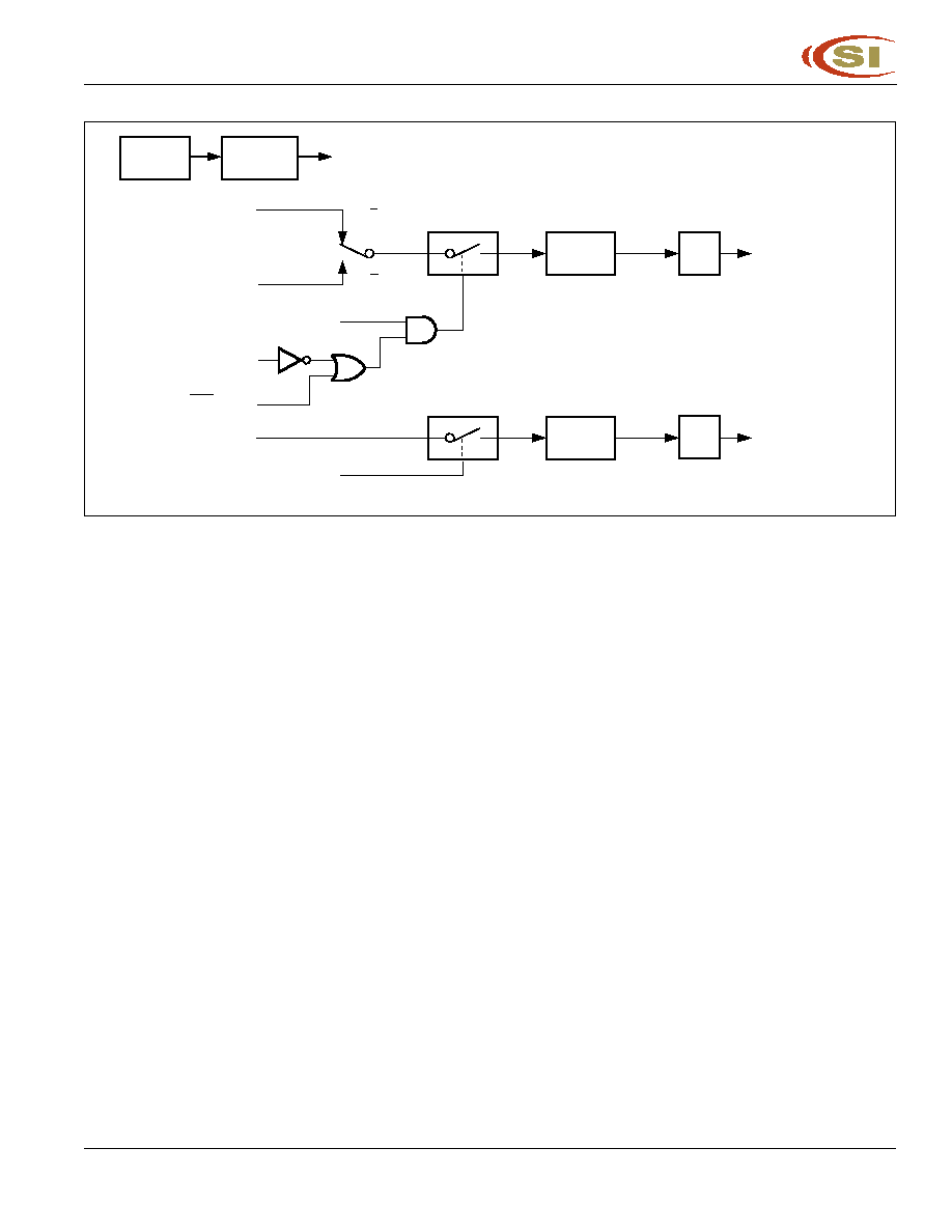
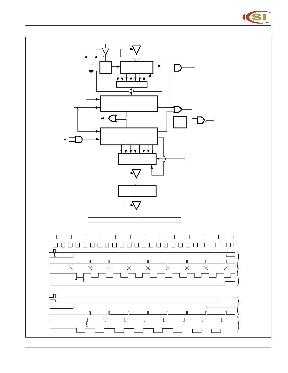
More About Mode 0
Serial data enters and exits through RXD. TXD outputs the
shift clock. Eight data bits are transmitted/received, with
the LSB first. The baud rate is fixed at 1/12 the oscillator
frequency.
Figure 15 shows a simplified functional diagram of the
serial port in Mode 0 and associated timing.
Transmission is initiated by any instruction that uses SBUF
as a destination register. The "write to SBUF" signal at
S6P2 also loads a 1 into the ninth position of the transmit
shift register and tells the TX Control block to begin a
transmission. The internal timing is such that one full
machine cycle will elapse between "write to SBUF" and
activation of SEND.
SEND transfer the output of the shift register to the alternate
output function line of P3.0, and also transfers SHIFT
CLOCK to the alternate output function line of P3.1. SHIFT
CLOCK is low during S3, S4, and S5 of every machine
cycle, and high during S6, S1, and S2. At S6P2 of every
machine cycle in which SEND is active, the contents of the
transmit shift register are shifted one position to the right.
As data bits shift out to the right, 0s come in from the left.
When the MSB of the data byte is at the output position of
the shift register, the 1 that was initially loaded into the ninth
position is just to the left of the MSB, and all positions to the
left of that contain 0s. This condition flags the TX Control
block to do one last shift, then deactivate SEND and set TI.
Both of these actions occur at S1P1 of the tenth machine
cycle after "write to SBUF."
Reception is initiated by the condition REN = 1 and
RI = 0. At S6P2 of the next machine cycle, the RX Control
unit writes the bits 11111110 to the receive shift register
and activates RECEIVE in the next clock phase.
RECEIVE enables SHIFT CLOCK to the alternate output
function line of P3.1. SHIFT CLOCK makes transitions at
S3P1 and S6P1 of every machine cycle. At S6P2 of every
machine cycle in which RECEIVE is active, the contents of
the receive shift register are shifted on position to the left.
The value that comes in from the right is the value that was
sampled at the P3.0 pin at S5P2 of the same machine
cycle.
As data bits come in from the right, 1s shift out to the left.
When the 0 that was initially loaded into the right-most
position arrives at the left-most position in the shift register,
it flags the RX Control block to do one last shift and load
SBUF. At S1P1 of the tenth machine cycle after the write
to SCON that cleared RI, RECEIVE is cleared and RI is set.
More About Mode 1
Ten bits are transmitted (through TXD), or received (through
RXD): a start bit (0), eight data bits (LSB first), and a stop
bit (1). On receive, the stop bit goes into RB8 in SCON. In
the IC80C52 the baud rate is determined by the Timer 1
overflow rate.
Figure 16 shows a simplified functional diagram of the
serial port in Mode 1 and associated timings for transmit
and receive.
Transmission is initiated by any instruction that uses SBUF
as a destination register.
The "write to SBUF" signal also loads a 1 into the ninth bit
position of the transmit shift register and flags the TX
control unit that a transmission is requested. Transmission
actually commences at S1P1 of the machine cycle following
the next rollover in the divide-by-16 counter. Thus, the bit
times are synchronized to the divide-by-16 counter, not to
the "write to SBUF" signal.
The transmission begins when SEND is activated, which
puts the start bit at TXD. One bit time later, DATA is
activated, which enables the output bit of the transmit shift
register to TXD. The first shift pulse occurs one bit time after
that.
As data bits shift out to the right, 0s are clocked in from the
left. When the MSB of the data byte is at the output position
of the shift register, the 1 that was initially loaded into the
ninth position is just to the left of the MSB, and all positions
to the left of that contain 0s. This condition flags the TX
Control unit to do one last shift, then deactivate SEND and
set TI. This occurs at the tenth divide-by-16 rollover after
"write to SBUF".
Reception is initiated by a 1-to-0 transition detected at
RXD. For this purpose, RXD is sampled at a rate of 16 times
the established baud rate. When a transition is detected,
the divide-by-16 counter is immediately reset, and 1FFH is
written into the input shift register. Resetting the divide-by-
16 counter aligns its rollovers with the boundaries of the
incoming bit times.
The 16 states of the counter divide each bit time into 16th.
At the seventh, eighth, and ninth counter states of each bit
time, the bit detector samples the value of RXD. The value
accepted is the value that was seen in at least two of the
three samples. This is done to reject noise. In order to reject
false bits, if the value accepted during the first bit time is not
0, the receive circuits are reset and the unit continues
looking for another 1-to-0 transition. If the start bit is valid,
it is shifted into the input shift register, and reception of the
rest of the frame proceeds.
As data bits come in from the right, 1s shift to the left. When

IC80C52
IC80C32
24
Integrated Circuit Solution Inc.
MC002-0B
the start bit arrives at the leftmost position in the shift
register, (which is a 9-bit register in Mode 1), it flags the RX
Control block to do one last shift, load SBUF and RB8, and
set RI. The signal to load SBUF and RB8 and to set RI is
generated if, and only if, the following conditions are met at
the time the final shift pulse is generated.
1) RI = 0 and
2) Either SM2 = 0, or the received stop bit =1
If either of these two conditions is not met, the received
frame is irretrievably lost. If both conditions are met, the
stop bit goes into RB8, the eight data bits go into SBUF, and
RI is activated. At this time, whether or not the above
conditions are met, the unit continues looking for a 1-to-0
transition in RXD.
More About Modes 2 and 3
Eleven bits are transmitted (through TXD), or received
(through RXD): a start bit (0), eight data bits (LSB first), a
programmable ninth data bit, and a stop bit (1). On transmit,
the ninth data bit (TB8) can be assigned the value of 0 or
1. On receive, the ninth data bit goes into RB8 in SCON.
The baud rate is programmable to either 1/32 or
1/64 of the oscillator frequency in Mode 2. Mode 3 may
have a variable baud rate generated from Timer 1 or 2.
Figures 17 and 18 show a functional diagram of the serial
port in Modes 2 and 3. The receive portion is exactly the
same as in Mode 1. The transmit portion differs from Mode
1 only in the ninth bit of the transmit shift register.
Transmission is initiated by any instruction that uses SBUF
as a destination register. The "write to SBUF" signal also
loads TB8 into the ninth bit position of the transmit shift
register and flags the TX Control unit that a transmission is
requested. Transmission commences at S1P1 of the
machine cycle following the next rollover in the divide-by-
16 counter. Thus, the bit times are synchronized to the
divide-by-16 counter, not to the "write to SBUF" signal.
The transmission begins when SEND is activated, which
puts the start bit at TXD. One bit timer later, DATA is
activated, which enables the output bit of the transmit shift
register to TXD. The first shift pulse occurs one bit time after
that. The first shift clocks a 1 (the stop bit) into the ninth bit
position of the shift register. Thereafter, only 0s are clocked
in. Thus, as data bits shift out to the right, 0s are clocked in
from the left. When TB8 is at the output position of the shift
register, then the stop bit is just to the left of TB8, and all
positions to the left of that contain 0s. This condition flags
the TX Control unit to do one last shift, then deactivate
SEND and set TI. This occurs at the eleventh divide-by-16
rollover after "write to SBUF".
Reception is initiated by a 1-to-0 transition detected at
RXD. For this purpose, RXD is sampled at a rate of 16 times
the established baud rate. When a transition is detected,
the divide-by-16 counter is immediately reset, and 1FFH is
written to the input shift register.
At the seventh, eighth, and ninth counter states of each bit
time, the bit detector samples the value of RXD. The value
accepted is the value that was seen in at least two of the
three samples. If the value accepted during the first bit time
is not 0, the receive circuits are reset and the unit continues
looking for another 1-to-0 transition. If the start bit proves
valid, it is shifted into the input shift register, and reception
of the rest of the frame proceeds.
As data bits come in from the right, 1s shift out to the left.
When the start bit arrives at the leftmost position in the shift
register (which in Modes 2 and 3 is a 9-bit register), it flags
the RX Control block to do one last shift, load SBUF and
RB8, and set RI. The signal to load SBUF and RB8 and to
set RI is generated if, and only if, the following conditions
are met at the time the final shift pulse is generated:
1) RI = 0, and
2) Either SM2 = 0 or the received ninth data bit = 1
If either of these conditions is not met, the received frame
is irretrievably lost, and RI is not set. If both conditions are
met, the received ninth data bit goes into RB8, and the first
eight data bits go into SBUF. One bit time later, whether the
above conditions were met or not, the unit continues
looking for a 1-to-0 transition at the RXD input.
Note that the value of the received stop bit is irrelevant to
SBUF, RB8, or RI.
Table 10. Serial Port Setup
Mode
SCON
SM2Variation
0
10H
1
50H
2
90H
3
D0H
0
NA
1
70H
2
B0H
3
F0H
Single Processor
Environment
(SM2 = 0)
Multiprocessor
Environment
(SM2 = 1)
Integrated Circuit Solution Inc.
25
MC002-0B
IC80C52
IC80C32
Figure 15. Serial Port Mode 0
WRITE
TO
SBUF
LOAD
SBUF
REN
RI
SBUF
ZERO DETECTOR
SHIFT
SHIFT
RXD
P3.0 ALT
OUTPUT
FUNCTION
TXD
P3.1 ALT
OUTPUT
FUNCTION
RXD
P3.0 ALT
INPUT
FUNCTION
Q
S
D
CL
START
TX CLOCK
RX CLOCK
START
SHIFT
SEND
RECEIVE
SHIFT
TX CONTROL
S6
SERIAL
PORT
INTERRUPT
SHIFT
CLOCK
RI
RX CONTROL
1 1 1 1 1 1 1 0
INPUT SHIFT REG.
SBUF
IC80C52/32 INTERNAL BUS
READ
SBUF
S4 S5 S6 S1 S2 S3 S4 S5 S6 S1 S2 S3 S4 S5 S6 S1 S2 S3 S4 S5 S6 S1 S2 S3 S4 S5 S6 S1 S2 S3 S4 S5 S6 S1 S2 S3 S4 S5 S6 S1 S2 S3 S4 S5 S6 S1 S2 S3 S4 S5 S6 S1 S2 S3 S4 S5 S6 S1 S2 S3 S4 S5 S6 S1 S2 S3 S4 S5 S6 S1 S2 S3 S4 S5 S6 S1
ALE
SEND
SHIFT
SHIFT
TI
RXD (D
OUT
)
TXD (SHIFT CLOCK)
WRITE TO SBUF
S6P2
S5P2
S6P1
S3P1
D0
D1
D2
D3
D5
D6
D7
D4
RI
RECEIVE
RXD (D
IN
)
TXD (SHIFT CLOCK)
WRITE TO SCON (CLEAR RI)
D0
D1
D2
D3
D5
D6
D7
D4
TRANSMIT
RECEIVE

IC80C52
IC80C32
26
Integrated Circuit Solution Inc.
MC002-0B
Figure 16. Serial Port Mode 1
WRITE
TO
SBUF
LOAD
SBUF
BIT
DETECTOR
INPUT SHIFT REG.
(9 BITS)
SAMPLE
RCLK
"0"
"0"
"1"
"1"
TCLK
SMOD
= 1
SMOD
= 0
SBUF
ZERO DETECTOR
SHIFT
RXD
TXD
Q
S
D
CL
START
RX CLOCK
RX CLOCK
START
DATA
SEND
LOAD
SBUF
SHIFT
1FFH
TX CONTROL
SERIAL
PORT
INTERRUPT
RI
RX CONTROL
SBUF
IC80C52/32 INTERNAL BUS
READ
SBUF
S1P1
D0
D1
D2
D3
D5
D6
D7
D4
D0
D1
D2
D3
D5
D6
D7
D4
SEND
DATA
SHIFT
SHIFT
TX CLOCK
WRITE TO SBUF
TRANSMIT
RECEIVE
SHIFT
TI
16
16
1-TO-0
TRANSITION
DETECTOR
IC80C52/32 INTERNAL BUS
TIMER 1
OVERFLOW
TIMER 2
OVERFLOW
2
TB8
STOP BIT
STOP BIT
START
BIT
START
BIT
TXD
RXD
BIT DETECTOR SAMPLE TIMES
TI
RI
RX
CLOCK
16 RESET

Integrated Circuit Solution Inc.
27
MC002-0B
IC80C52
IC80C32
Figure 17. Serial Port Mode 2
WRITE
TO
SBUF
LOAD
SBUF
BIT
DETECTOR
INPUT SHIFT REG.
(9 BITS)
SAMPLE
MODE 2
(SMOD IS PCON. 7)
SBUF
ZERO DETECTOR
SHIFT
RXD
TXD
Q
S
D
CL
START
TX CLOCK
START
DATA
SEND
LOAD
SBUF
SHIFT
1FFH
TX CONTROL
SERIAL
PORT
INTERRUPT
RI
RX CONTROL
SBUF
IC80C52/32 INTERNAL BUS
READ
SBUF
S1P1
D0
D1
D2
D3
D5
D6
D7
TB8
D4
SEND
DATA
SHIFT
SHIFT
TX
CLOCK
WRITE TO SBUF
TRANSMIT
RECEIVE
SHIFT
TI
16
16
1-TO-0
TRANSITION
DETECTOR
IC80C52/32 INTERNAL BUS
PHASE 2 CLOCK
(1/2 f
OSC
)
2
TB8
STOP BIT
TXD
BIT DETECTOR SAMPLE TIMES
TI
RI
STOP BIT GEN
STOP BIT GEN
RX
CLOCK
SMOD 0
SMOD 1
D0
D1
D2
D3
D5
D6
D7
D4
STOP
BIT
RXD
RX
CLOCK
16 RESET
RB8
START
BIT
START
BIT

IC80C52
IC80C32
28
Integrated Circuit Solution Inc.
MC002-0B
Figure 18. Serial Port Mode 3
SHIFT
RECEIVE
BIT DETECTOR SAMPLE TIMES
RI
D0
D1
D2
D3
D5
D6
D7
D4
STOP
BIT
RXD
RX
CLOCK
16 RESET
RB8
WRITE
TO
SBUF
LOAD
SBUF
BIT
DETECTOR
INPUT SHIFT REG.
(9 BITS)
SAMPLE
RCLK
"0"
"0"
"1"
"1"
TCLK
SMOD
= 1
SMOD
= 0
SBUF
ZERO DETECTOR
SHIFT
RXD
TXD
Q
S
D
CL
START
RX CLOCK
RX CLOCK
START
DATA
SEND
LOAD
SBUF
SHIFT
1FFH
TX CONTROL
SERIAL
PORT
INTERRUPT
RI
RX CONTROL
SBUF
IC80C52/32 INTERNAL BUS
READ
SBUF
S1P1
D0
D1
D2
D3
D5
D6
TB8
D7
D4
SEND
DATA
SHIFT
TX
CLOCK
WRITE TO SBUF
TRANSMIT
SHIFT
TI
16
16
1-TO-0
TRANSITION
DETECTOR
IC80C52/32 INTERNAL BUS
TIMER 1
OVERFLOW
TIMER 2
OVERFLOW
2
TB8
STOP BIT
TXD
TI
STOP BIT GEN
START
BIT
START
BIT

Integrated Circuit Solution Inc.
29
MC002-0B
IC80C52
IC80C32
INTERRUPT SYSTEM
The IC80C52/32 provides six interrupt sources: two external
interrupts, two timer interrupts, and a serial port interrupt.
These are shown in Figure 19.
The External Interrupts
INT0 and INT1 can each be either
level-activated or transition-activated, depending on bits
IT0 and IT1 in Register TCON. The flags that actually
generate these interrupts are the IE0 and IE1 bits in TCON.
When the service routine is vectored, hardware clears the
flag that generated an external interrupt only if the interrupt
was transition-activated. If the interrupt was level-activated,
then the external requesting source (rather than the on-
chip hardware) controls the request flag.
The Timer 0 and Timer 1 Interrupts are generated by TF0
and TF1, which are set by a rollover in their respective
Timer/Counter registers (except for Timer 0 in Mode 3).
When a timer interrupt is generated, the on-chip hardware
clears the flag that generated it when the service routine is
vectored to.
The Serial Port Interrupt is generated by the logical OR of
RI and TI. Neither of these flags is cleared by hardware
when the service routine is vectored to. In fact, the service
routine normally must determine whether RI or TI generated
the interrupt, and the bit must be cleared in software.
In the IC80C52/32, the Timer 2 Interrupt is generated by the
logical OR of TF2 and EXF2. Neither of these flags is
cleared by hardware when the service routine is vectored
to. In fact, the service routine may have to determine
whether TF2 or EXF2 generated the interrupt, and the bit
must be cleared in software.
All of the bits that generate interrupts can be set or cleared
by software, with the same result as though they had been
set or cleared by hardware. That is, interrupts can be
generated and pending interrupts can be canceled in
software.
Each of these interrupt sources can be individually enabled
or disabled by setting or clearing a bit in Special Function
Register IE (interrupt enable) at address 0A8H. As well as
individual enable bits for each interrupt source, there is a
global enable/disable bit that is cleared to disable all
interrupts or set to turn on interrupts (see SFR IE).
Figure 19. Interrupt System
INT1
INTERNAL
SERIAL
PORT
T2EX
SCON.0
RI
SCON.1
TI
TIMER/COUNTER 1
TCON.7
TF1
EXTERNAL
INT RQST 1
TCON.3
IE1
TIMER/COUNTER 0
TCON.5
TF0
EXTERNAL
INT RQST 0
TCON.1
IE0
INT0
IE.4
IE.3
ET1
IE.2
EX1
IE.1
ET0
IE.0
EX0
IE.7
IP.4
PS
TIMER/
COUNTER 2
T2CON.7
TF2
T2CON.6
EXF2
IE.5
IP.5
PT2
ET2
EA
IP.3
PT1
IP.2
PX1
IP.1
PT0
IP.0
PX0
POLLING
HARDWARE
SOURCE
I.D.
HIGH PRIORITY
INTERRUPT
REQUEST
VECTOR
SOURCE
I.D.
LOW PRIORITY
INTERRUPT
REQUEST
VECTOR
ES
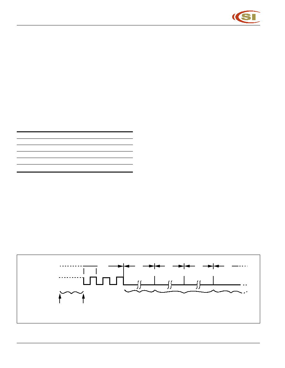
IC80C52
IC80C32
30
Integrated Circuit Solution Inc.
MC002-0B
Priority Level Structure
Each interrupt source can also be individually programmed
to one of two priority levels by setting or clearing a bit in
Special Function Register IP (interrupt priority) at address
0B8H. IP is cleared after a system reset to place all
interrupts at the lower priority level by default. A low-priority
interrupt can be interrupted by a high-priority interrupt but
not by another low-priority interrupt. A high-priority interrupt
can not be interrupted by any other interrupt source.
If two requests of different priority levels are received
simultaneously, the request of higher priority level is
serviced. If requests of the same priority level are received
simultaneously, an internal polling sequence determines
which request is serviced. Thus, within each priority level
there is a second priority structure determined by the
polling sequence, as follows:
Source
Priority Within Level
1.
IE0
(Highest)
2.
TF0
3.
IE1
4.
R1 + T1
5.
TF2 + EXF2
(Lowest)
Note that the "priority within level" structure is only used to
resolve simultaneous requests of the same priority level.
How Interrupts Are Handled
The interrupt flags are sampled at S5P2 of every machine
cycle. The samples are polled during the following machine
cycle (the Timer 2 interrupt cycle is different, as described
in the Response Timer Section). If one of the flags was in
a set condition at S5P2 of the preceding cycle, the polling
cycle will find it and the interrupt system will generate an
LCALL to the appropriate service routine, provided this
hardware generated LCALL is not blocked by any of the
following conditions:
1. An interrupt of equal or higher priority level is already
in progress.
2. The current (polling) cycle is not the final cycle in the
execution of the instruction in progress.
3. The instruction in progress is RETI or any write to the
IE or IP registers.
Any of these three conditions will block the generation of
the LCALL to the interrupt service routine. Condition 2
ensures that the instruction in progress will be completed
before vectoring to any service routine. Condition 3 ensures
that if the instruction in progress is RETI or any access to
IE or IP, then at least one more instruction will be executed
before any interrupt is vectored to.
The polling cycle is repeated with each machine cycle, and
the values polled are the values that were present at S5P2
of the previous machine cycle. If an active interrupt flag is
not being serviced because of one of the above conditions
and is not still active when the blocking condition is removed,
the denied interrupt will not be serviced. In other words, the
fact that the interrupt flag was once active but not serviced
is not remembered. Every polling cycle is new. The polling
cycle/LCALL sequence is illustrated in Figure 20.
Note that if an interrupt of higher priority level goes active
prior to S5P2 of the machine cycle labeled C3 in Figure 20,
then in accordance with the above rules it will be serviced
during C5 and C6, without any instruction of the lower
priority routine having been executed.
Figure 20. Interrupt Response Timing Diagram
INTERRUPT
GOES ACTIVE
INTERRUPTS
ARE POLLED
INTERRUPT
ROUTINE
LONG CALL TO
INTERRUPT
VECTOR ADDRESS
INTERRUPT
LATCHED
C4
C3
C2
C1
C5
S5P2
S6
E

Integrated Circuit Solution Inc.
31
MC002-0B
IC80C52
IC80C32
Thus, the processor acknowledges an interrupt request by
executing a hardware-generated LCALL to the appropriate
servicing routine. In some cases it also clears the flag that
generated the interrupt, and in other cases it does not. It
never clears the Serial Port or Timer 2 flags. This must be
done in the user's software. The processor clears an
external interrupt flag (IE0 or IE1) only if it was transition-
activated. The hardware-generated LCALL pushes the
contents of the Program Counter onto the stack (but it does
not save the PSW) and reloads the PC with an address that
depends on the source of the interrupt being serviced, as
shown in the following table.
Interrupt
Interrupt
Cleared by
Vector
Source
Request Bits
Hardware
Address
INT0
IE0
No (level)
0003H
Yes (trans.)
Timer 0
TF0
Yes
000BH
INT1
IE1
No (level)
0013H
Yes (trans.)
Timer 1
TF1
Yes
001BH
Serial Port
RI, TI
No
0023H
Timer 2
TF2, EXF2
No
002BH
System
RST
0000H
Reset
Execution proceeds from that location until the RETI
instruction is encountered. The RETI instruction informs
the processor that this interrupt routine is no longer in
progress, then pops the top two bytes from the stack and
reloads the Program Counter. Execution of the interrupted
program continues from where it left off.
Note that a simple RET instruction would also have returned
execution to the interrupted program, but it would have left
the interrupt control system thinking an interrupt was still in
progress.
SFR Register and
Interrupt
Flag
Bit Position
External 0
IE0
TCON.1
External 1
IE1
TCON.3
Timer 1
TF1
TCON.7
Timer 0
TF0
TCON.5
Serial Port
TI
SCON.1
Serial Port
RI
SCON.0Timer 2
TF2
T2CON.7
Timer 2
EXF2
T2CON.6
When an interrupt is accepted, the following action occurs:
1. The current instruction completes operation.
2. The PC is saved on the stack.
3. The current interrupt status is saved internally.
4. Interrupts are blocked at the level of the interrupts.
5. The PC is loaded with the vector address of the ISR
(interrupts service routine).
6. The ISR executes.
The ISR executes and takes action in response to the
interrupt. The ISR finishes with RETI (return from interrupt)
instruction. This retrieves the old value of the PC from the
stack and restores the old interrupt status. Execution of the
main program continues where it left off.
External Interrupts
The external sources can be programmed to be level-
activated or transition-activated by setting or clearing bit
IT1 or IT0 in Register TCON. If ITx= 0, external interrupt x
is triggered by a detected low at the
INTx pin. If ITx = 1,
external interrupt x is edge-triggered. In this mode if
successive samples of the
INTx pin show a high in one
cycle and a low in the next cycle, interrupt request flag IEx
in TCON is set. Flag bit IEx then requests the interrupt.
Since the external interrupt pins are sampled once each
machine cycle, an input high or low should hold for at least
12 oscillator periods to ensure sampling. If the external
interrupt is transition-activated, the external source has to
hold the request pin high for at least one machine cycle,
and then hold it low for at least one machine cycle to ensure
that the transition is seen so that interrupt request flag IEx
will be set. IEx will be automatically cleared by the CPU
when the service routine is called.
If the external interrupt is level-activated, the external
source has to hold the request active until the requested
interrupt is actually generated. Then the external source
must deactivate the request before the interrupt service
routine is completed, or else another interrupt will be
generated.

IC80C52
IC80C32
32
Integrated Circuit Solution Inc.
MC002-0B
Response Time
The
INT0 and INT1 levels are inverted and latched into the
interrupt flags IE0 and IE1 at S5P2 of every machine cycle.
Similarly, the Timer 2 flag EXF2 and the Serial Port flags RI
and TI are set at S5P2. The values are not actually polled
by the circuitry until the next machine cycle.
The Timer 0 and Timer 1 flags, TF0 and TF1, are set at
S5P2 of the cycle in which the timers overflow. The values
are then polled by the circuitry in the next cycle. However,
the Timer 2 flag TF2 is set at S2P2 and is polled in the same
cycle in which the timer overflows.
If a request is active and conditions are right for it to be
acknowledged, a hardware subroutine call to the requested
service routine will be the next instruction executed. The
call itself takes two cycles. Thus, a minimum of three
complete machine cycles elapsed between activation of an
external interrupt request and the beginning of execution of
the first instruction of the service routine. Figure 19 shows
response timings.
A longer response time results if the request is blocked by
one of the three previously listed conditions. If an interrupt
of equal or higher priority level is already in progress, the
additional wait time depends on the nature of the other
interrupt's service routine. If the instruction in progress is
not in its final cycle, the additional wait time cannot be more
than three cycles, since the longest instructions (MUL and
DIV) are only four cycles long. If the instruction in progress
is RETI or an access to IE or IP, the additional wait time
cannot be more than five cycles (a maximum of one more
cycle to complete the instruction in progress, plus four
cycles to complete the next instruction if the instruction is
MUL or DIV).
Thus, in a single-interrupt system, the response time is
always more than three cycles and less than nine cycles.
Single-Step Operation
The IC80C54/58 interrupt structure allows single-step
execution with very little software overhead. As previously
noted, an interrupt request will not be serviced while an
interrupt of equal priority level is still in progress, nor will it
be serviced after RETI until at least one other instruction
has been executed. Thus, once an interrupt routine has
been entered, it cannot be re-entered until at least one
instruction of the interrupted program is executed. One
way to use this feature for single-step operation is to
program one of the external interrupts (for example,
INT0)
to be level-activated. The service routine for the interrupt
will terminate with the following code:
JNB
P3.2,$
;Wait Here Till
INT0 Goes High
JB
P3.2,$
;Now Wait Here Till it Goes Low
RETI
; G o B a c k a n d E x e c u t e O n e
Instruction
If the
INT0 pin, which is also the P3.2 pin, is held normally
low, the CPU will go right into the External Interrupt 0
routine and stay there until INT0 is pulsed (from low-to-
high-to-low). Then it will execute RETI, go back to the task
program, execute one instruction, and immediately re-
enter the External Interrupt 0 routine to await the next
pulsing of P3.2. One step of the task program is executed
each time P3.2 is pulsed.

Integrated Circuit Solution Inc.
33
MC002-0B
IC80C52
IC80C32
Table 11. Reset Values of the SFR's
SFR Name
Reset Value
PC
0000H
ACC
00H
B
00H
PSW
00H
SP
07H
DPTR
0000H
P0-P3
FFH
IP
XX000000B
IE
0X000000B
TMOD
00H
TCON
00H
T2CON
00H
TH0
00H
TL0
00H
TH1
00H
TL1
00H
TH2
00H
TL2
00H
RCAP2H
00H
RCAP2L
00H
SCON
00H
SBUF
Indeterminate
PCON
0XXX0000B
OTHER INFORMATION
Reset
The reset input is the RST pin, which is the input to a
Schmitt Trigger.
A reset is accomplished by holding the RST pin high for at
least two machine cycles (24 oscillator periods), while the
oscillator is running. The CPU responds by generating an
internal reset, with the timing shown in Figure 21.
The external reset signal is asynchronous to the internal
clock. The RST pin is sampled during State 5 Phase 2 of
every machine cycle. The port pins will maintain their
current activities for 19 oscillator periods after a logic 1 has
been sampled at the RST pin; that is, for 19 to 31 oscillator
periods after the external reset signal has been applied to
the RST pin.
The internal reset algorithm writes 0s to all the SFRs except
the port latches, the Stack Pointer, and SBUF. The port
latches are initialized to FFH, the Stack Pointer to 07H, and
SBUF is indeterminate. Table 9 lists the SFRs and their
reset values.
Then internal RAM is not affected by reset. On power-up
the RAM content is indeterminate.

IC80C52
IC80C32
34
Integrated Circuit Solution Inc.
MC002-0B
Power-on Reset
An automatic reset can be obtained when V
CC
goes through
a 10µF capacitor and GND through an 8.2K resistor,
providing the Vcc rise time does not exceed 1 msec and the
oscillator start-up time does not exceed 10 msec. This
Power-on reset circuit is shown if Figure 21. The CMOS
devices do not require the 8.2K pulldown resistor, although
its presence does no harm.
When power is turned on, the circuit holds the RST pin high
for an amount of time that depends on the value of the
capacitor and the rate at which it charges. To ensure a good
reset, the RST pin must be high long enough to allow the
oscillator time to start-up (normally a few msec) plus two
machine cycles.
Note that the port pins will be in a random state until the
oscillator has start and the internal reset algorithm has
written 1s to them.
With this circuit, reducing V
CC
quickly to 0 causes the RST
pin voltage to momentarily fall below 0V. However, this
voltage is internally limited and will not harm the device.
Figure 21. Power-On Reset Circuit
Vcc
RST
GND
Vcc
IC80C52/32
10 F
8.2K
+
-
Figure 22. Reset Timing
12 OSC. PERIODS
ALE
RST
SAMPLE
RST
SAMPLE
RST
INTERNAL RESET SIGNAL
PSEN
P0
11 OSC. PERIODS
INST
ADDR
INST
INST
INST
19 OSC. PERIODS
S5 S6 S1 S2 S3 S4 S5 S6 S1 S2 S3 S4 S5 S6 S1 S2 S3 S4
ADDR
ADDR
ADDR
INST
ADDR
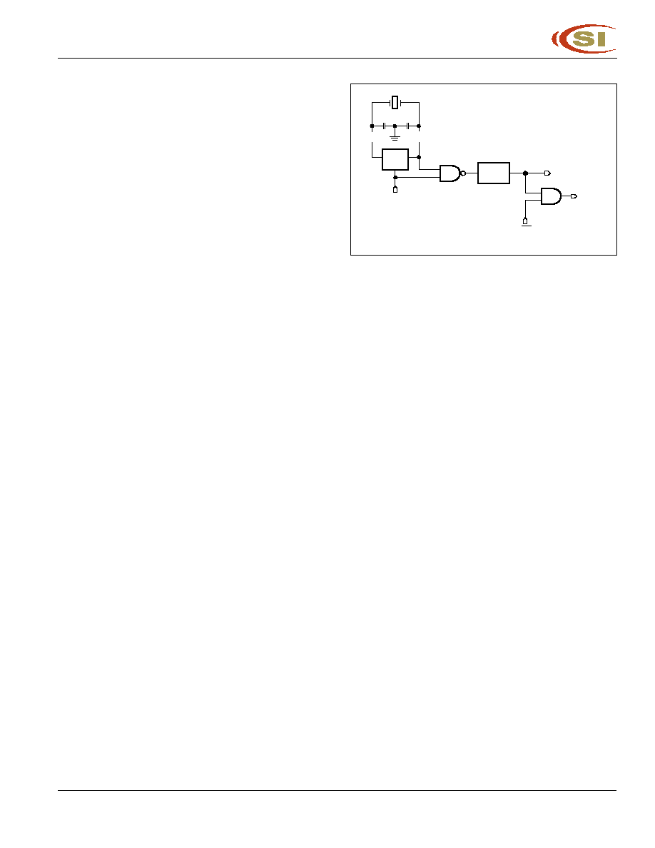
Integrated Circuit Solution Inc.
35
MC002-0B
IC80C52
IC80C32
Power-Saving Modes of Operation
The IC80C52/32 has two power-reducing modes. Idle and
Power-down. The input through which backup power is
supplied during these operations is Vcc. Figure 23 shows
the internal circuitry which implements these features. In
the Idle mode (IDL = 1), the oscillator continues to run and
the Interrupt, Serial Port, and Timer blocks continue to be
clocked, but the clock signal is gated off to the CPU. In
Power-down (PD = 1), the oscillator is frozen. The Idle and
Power-down modes are activated by setting bits in Special
Function Register PCON.
Idle Mode
An instruction that sets PCON.0 is the last instruction
executed before the Idle mode begins. In the Idle mode, the
internal clock signal is gated off to the CPU, but not to the
Interrupt, Timer, and Serial Port functions. The CPU status
is preserved in its entirety; the Stack Pointer, Program
Counter, Program Status Word, Accumulator, and all other
registers maintain their data during Idle. The port pins hold
the logical states they had at the time Idle was activated.
ALE and
PSEN hold at logic high levels.
There are two ways to terminate the Idle. Activation of any
enabled interrupt will cause PCON.0 to be cleared by
hardware, terminating the Idle mode. The interrupt will be
serviced, and following RETI the next instruction to be
executed will be the one following the instruction that put
the device into Idle.
The flag bits GF0 and GF1 can be used to indicate whether
an interrupt occurred during normal operation or during an
Idle. For example, an instruction that activates Idle can also
set one or both flag bits. When Idle is terminated by an
interrupt, the interrupt service routine can examine the flag
bits.
The other way of terminating the Idle mode is with a
hardware reset. Since the clock oscillator is still running,
the hardware reset must be held active for only two
machine cycles (24 oscillator periods) to complete the
reset.
The signal at the RST pin clears the IDL bit directly and
asynchronously. At this time, the CPU resumes program
execution from where it left off; that is, at the instruction
following the one that invoked the Idle Mode. As shown in
Figure 22, two or three machine cycles of program execution
may take place before the internal reset algorithm takes
control. On-chip hardware inhibits access to the internal
RAM during his time, but access to the port pins is not
inhibited. To eliminate the possibility of unexpected outputs
at the port pins, the instruction following the one that
invokes Idle should not write to a port pin or to external data
RAM.
Power-down Mode
An instruction that sets PCON.1 is the last instruction
executed before Power-down mode begins. In the Power-
down mode, the on-chip oscillator stops. With the clock
frozen, all functions are stopped, but the on-chip RAM and
Special function Registers are held. The port pins output
the values held by their respective SFRs. ALE and
PSEN
output lows.
In the Power-down mode of operation, Vcc can be reduced
to as low as 2V. However, Vcc must not be reduced before
the Power-down mode is invoked, and Vcc must be restored
to its normal operating level before the Power-down mode
is terminated. The reset that terminates Power-down also
frees the oscillator. The reset should not be activated
before Vcc is restored to its normal operating level and
must be held active long enough to allow the oscillator to
restart and stabilize (normally less than 10 msec).
The only exit from Power-down is a hardware reset. Reset
redefines all the SFRs but does not change the on-chip
RAM.
OSC
CLOCK
GEN
PD
XTAL 1
XTAL 2
IDL
CPU
INTERRUPT,
SERIAL PORT,
TIMER BLOCKS
Figure 23. Idle and Power-Down Hardware
IC80C52
IC80C32
36
Integrated Circuit Solution Inc.
MC002-0B
Table 12. Status of the External Pins During Idle and Power-down Modes.
Mode
Memory
ALE
PSEN
PSEN
PSEN
PSEN
PSEN
PORT 0
PORT 1
PORT 2
PORT 3
Idle
Internal
1
1
Data
Data
Data
Data
Idle
External
1
1
Float
Data
Address
Data
Power-down
Internal
0
0
Data
Data
Data
Data
Power-down
External
0
0
Float
Data
Data
Data
On-Chip Oscillators
The on-chip oscillator circuitry of the IC80C54/58 is a single
stage inverter, intended for use as a crystal-controlled,
positive reactance oscillator. In this application the crystal is
operated in its fundamental response mode as an inductive
reactance in parallel resonance with capacitance external to
the crystal (Figure 24). Examples of how to drive the clock
with external oscillator are shown in Figure 25.
Figure 24. Oscillator Connections
The crystal specifications and capacitance values (C1 and
C2 in Figure 24) are not critical. 20 pF to 30 pF can be used
in these positions at a 12 MHz to 24 MHz frequency with
good quality crystals. (For ranges greater than 24 MHz refer
to Figure 26.) A ceramic resonator can be used in place of
the crystal in cost-sensitive applications. When a ceramic
resonator is used, C1 and C2 are normally selected to be of
somewhat higher values. The manufacturer of the ceramic
resonator should be consulted for recommendation on the
values of these capacitors.
GND
XTAL1
XTAL2
EXTERNAL
OSCILLATOR
SIGNAL
NC
Figure 25. External Clock Drive Configuration
C1
C2
GND
XTAL1
XTAL2
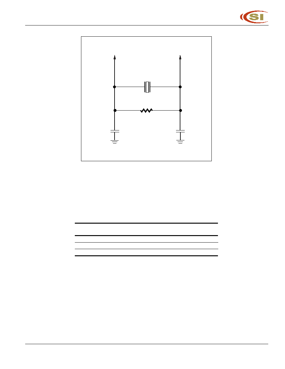
Integrated Circuit Solution Inc.
37
MC002-0B
IC80C52
IC80C32
Figure 26. Oscillator Connections for High Speed (> 24 MHz)
Note:
When the frequency is higher than 24 MHz, please refer to Table 13 for recommended values of C1, C2, and R.
XTAL2
XTAL1
C1
C2
R
Table 13. Recommended Value for C1, C2, R
Frequency Range
3.5 MHz - 24 MHz
24 MHz - 40 MHz
C1
20 pF-30 pF
3 pF-10 pF
C2
20 pF-30 pF
3 pF-10 pF
R
Not Apply
6.2K-10K
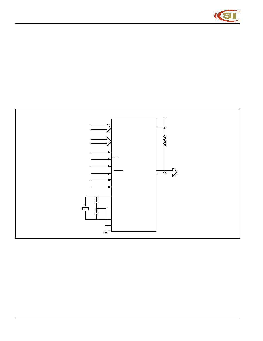
IC80C52
IC80C32
38
Integrated Circuit Solution Inc.
MC002-0B
ROM Verification
The address of the program menory location to be read is
applied to Port 1 and pins P2.4-P2.0. The other pins should
be held at the "Verify" level are indicated in Figure 26. The
contents of the addressed locations exits on Port 0. Exter-
nal pullups are required on Rort 0 for this operation. Fig-
ure 27 shows the setup to verify the program memory.
Figure 27. ROM Verification
XTAL2
GND
XTAL1
4-6 MHz
P1
P2.4-P2.0
RST
EA
ALE
PSEN
P2.7
P2.6
1
1
1
0
0
0
Vcc
P0
+ 5V
A7-A0
A12-A8
PGM
DATA
10K x 8

Integrated Circuit Solution Inc.
39
MC002-0B
IC80C52
IC80C32
ROM Lock System
The program lock system, when programmed, protects the
ROM code against software piracy. The IC80c52/32 has a
two-level program lock system (see Table 14) and a 32-
byte encryption table. No matter what lock bit is, the user
submits the encryption table with his or her code in verify
ROM mode. both the lock-bit and encryption array.
Encryption Array
Within the ROM array are 32 bytes of Encryption Array that
are initially unprogramed (all 1's). Every time that a byte is
addressed during verify, five address lines are used to
select a byte of the Encryption Array. This byte is then
exclusive-NOR'ed (XNOR) with the code byte, creating an
Encryption verify byte. The algorithm, with the array in the
unprogrammed state (all 1's), will return the code in its
original, unmodified form.
When using the encryption array, one important factor
needs to be considered, If a code byte has the value 0FFH,
verifying the byte will produce the encryption byte value. If
a large block (> 32 bytes) of code is left unprogrammed, a
verification routine will display the contents of the encryption
array. For this reason, all unused code bytes should be
programmed with some value other than 0FFH, and not all
of them the same value.
Table 14. Program Lock Bits
LB1
LB2
Protection Type
1
U
U
No program Lock Features enabled. (Code verify will still be encrypted by the
Encryption Array if Programmed
2
P
U
MOVC instructions executed from external program menory are diabled form
fetching code bytes from internal memory, EA is sampled and latched on Reset.
3
P
P
Same as 2, also ROM verify is disabled.

IC80C52
IC80C32
40
Integrated Circuit Solution Inc.
MC002-0B
OPERATING RANGE
(1)
Range
Ambient Temperature
V
CC
Oscillator Frequency
Commercial
0∞C to +70∞C
5V ± 10%
3.5 to 40 MHz
Note:
1. Operating ranges define those limits between which the functionality of the device is guaranteed.
ABSOLUTE MAXIMUM RATINGS
(1)
Symbol
Parameter
Value
Unit
V
TERM
Terminal Voltage with Respect to GND
(2)
≠2.0 to +7.0
V
T
BIAS
Temperature Under Bias
(3)
0 to +70
∞C
T
STG
Storage Temperature
≠65 to +125
∞C
P
T
Power Dissipation
1.5
W
Note:
1. Stress greater than those listed under ABSOLUTE MAXIMUM RATINGS may cause
permanent damage to the device. This is a stress rating only and functional operation
of the device at these or any other conditions above those indicated in the operational
sections of this specification is not implied. Exposure to absolute maximum rating
conditions for extended periods may affect reliability.
2. Minimum DC input voltage is ≠0.5V. During transitions, inputs may undershoot to ≠2.
0V for periods less than 20 ns. Maximum DC voltage on output pins is Vcc + 0.5V
which may overshoot to Vcc + 2.0V for periods less than 20 ns.
3. Operating temperature is for commercial products only defined by this specification.

Integrated Circuit Solution Inc.
41
MC002-0B
IC80C52
IC80C32
DC CHARACTERISTICS
(Ta=0∞C to 70 ∞C; VCC=5V+10%; VSS=0V )
Symbol
Parameter
Test conditions
Min
Max
Unit
V
IL
Input low voltage (All except
EA)
≠0.5
0.2Vcc ≠ 0.1
V
V
IL
1
Input low voltage (
EA)
≠0.5
0.2Vcc ≠ 0.3
V
V
IH
Input high voltage
0.2Vcc + 0.9
Vcc + 0.5
V
(All except XTAL 1, RST)
V
IH
1
Input high voltage (XTAL 1)
0.7Vcc
Vcc + 0.5
V
V
SCH
+
RST positive schmitt-trigger
0.7Vcc
Vcc + 0.5
V
threshold voltage
V
SCH
≠
RST negative schmitt-trigger
0
0.3Vcc
V
threshold voltage
V
OL
(1)
Output low voltage
Iol = 100 µA
--
0.3
V
(Ports 1, 2, 3)
I
OL
= 1.6 mA
--
0.45
V
I
OL
= 3.5 mA
--
1.0
V
V
OL
1
(1)
Output low voltage
I
OL
= 200 µA
--
0.3
V
(Port 0, ALE,
PSEN)
I
OL
= 3.2 mA
--
0.45
V
I
OL
= 7.0 mA
--
1.0
V
V
OH
Output high voltage
I
OH
= ≠10 µA
0.9Vcc
--
V
(Ports 1, 2, 3, ALE,
PSEN)
Vcc = 4.5V-5.5V
I
OL
= ≠25 µA
0.75Vcc
--
V
I
OL
= ≠60 µA
2.4
--
V
V
OH
1
Output high voltage
I
OH
= ≠80 µA
0.9Vcc
--
V
(Port 0, ALE,
PSEN)
Vcc = 4.5V-5.5V
I
OH
= ≠300 µA
0.75Vcc
--
V
I
OH
= ≠800 µA
2.4
--
V
I
IL
Logical 0 input current (Ports 1, 2, 3) V
IN
= 0.45V
--
≠50
µA
I
LI
Input leakage current (Port 0)
0.45V < V
IN
< Vcc
≠10
+10
µA
I
TL
Logical 1-to-0 transition current
V
IN
= 2.0V
--
≠650
µA
(Ports 1, 2, 3)
R
RST
RST pulldown resister
50
300
K
Note:
1. Under steady state (non-transient) conditions, I
OL
must be externally limited as follows:
Maximum I
OL
per port pin:
10 mA
Maximum I
OL
per 8-bit port
Port 0: 26 mA
Ports 1, 2, 3: 15 mA
Maximum total I
OL
for all output pins: 71 mA
If I
OL
exceeds the test condition, V
OL
may exceed the related specification.

IC80C52
IC80C32
42
Integrated Circuit Solution Inc.
MC002-0B
POWER SUPPLY CHARACTERISTICS
Symbol
Parameter
Test conditions
Min
Max
Unit
Icc
Power supply current
(1)
Vcc = 5.0V
Active mode
12 MHz
--
20
mA
16 MHz
--
26
mA
20 MHz
--
32
mA
24 MHz
--
38
mA
32 MHz
--
50
mA
40 MHz
--
62
mA
Idle mode
12 MHz
--
5
mA
16 MHz
--
6
mA
20 MHz
--
7.6
mA
24 MHz
--
9
mA
32 MHz
--
12
mA
40 MHz
--
15
mA
Power-down mode
V
CC
= 5V
--
100
µA
Note:
1. See Figures 28,29,30, and 31 for Icc test conditiions.
Figure 28. Active Mode
Figure 29. Idle Mode
Figure 30. Power-down Mode
XTAL1
GND
NC
RST
Vcc
P0
EA
Vcc
Vcc
CLOCK
SIGNAL
Icc
XTAL2
Vcc
XTAL1
GND
NC
RST
Vcc
P0
EA
Vcc
Vcc
CLOCK
SIGNAL
Icc
XTAL2
XTAL1
GND
NC
RST
Vcc
P0
EA
Vcc
Vcc
Icc
XTAL2

Integrated Circuit Solution Inc.
43
MC002-0B
IC80C52
IC80C32
Figure 31. Clock Signal Waveform for I
CC
Tests in Active and Idle Mode (t
CLCH
=t
CHCL
=5 ns)
EXTERNAL MEMORY CHARACTERISTICS
24 MHz
40 MHz
Variable Oscillator
Clock
Clock
(3.5 - 40 MHz)
Symbol
Parameter
Min
Max
Min Max
Min
Max
Unit
1/t
CLCL
Oscillator frequency
--
--
--
--
3.5
40
MHz
t
LHLL
ALE pulse width
68
--
35
--
2t
CLCL
≠15
--
ns
t
AVLL
Address valid to ALE low
26
--
10
--
t
CLCL
≠15
--
ns
t
LLAX
Address hold after ALE low
31
--
15
--
t
CLCL
≠10
--
ns
t
LLIV
ALE low to valid instr in
--
147
--
80
--
4t
CLCL
≠20
ns
t
LLPL
ALE low to
PSEN low
31
--
15
--
t
CLCL
≠10
--
ns
t
PLPH
PSEN pulse width
110
--
60
--
3t
CLCL
≠15
--
ns
t
PLIV
PSEN low to valid instr in
--
105
--
55
--
3t
CLCL
≠20
ns
t
PXIX
Input instr hold after
PSEN
0
--
0
--
0
--
ns
t
PXIZ
Input instr float after
PSEN
--
37
--
20
--
t
CLCL
≠5
ns
t
AVIV
Address to valid instr in
--
188
--
105
--
5t
CLCL
≠20
ns
t
PLAZ
PSEN low to address float
--
10
--
10
--
10
ns
t
RLRH
RD pulse width
230
--
130
--
6t
CLCL
≠20
--
ns
t
WLWH
WR pulse width
230
--
130
--
6t
CLCL
≠20
--
ns
t
RLDV
RD low to valid data in
--
157
--
90
--
4t
CLCL
≠10
ns
t
RHDX
Data hold after
RD
0
--
0
--
0
--
ns
t
RHDZ
Data float after
RD
--
78
--
45
--
2t
CLCL
≠5
ns
t
LLDV
ALE low to valid data in
--
282
--
165
--
7t
CLCL
≠10
ns
t
AVDV
Address to valid data in
--
323
--
190
--
8t
CLCL
≠10
ns
t
LLWL
ALE low to
RD or WR low
105
145
55
95
3t
CLCL
≠20
3t
CLCL
+20
ns
t
AVWL
Address to
RD or WR low
146
--
80
--
4t
CLCL
≠20
--
ns
t
QVWX
Data valid to
WR transition
26
--
10
--
t
CLCL
≠15
--
ns
t
WHQX
Data hold after
WR
31
--
15
--
t
CLCL
≠10
--
ns
t
RLAZ
RD low to address float
--
0
--
0
--
0
ns
t
WHLH
RD or WR high to ALE high
26
57
10
40
t
CLCL
≠15
t
CLCL
+15
ns
0.45V
Vcc -- 0.5V
t
CHCX
t
CLCL
t
CLCH
t
CLCX
t
CHCL
0.7Vcc
0.2Vcc -- 0.1

IC80C52
IC80C32
44
Integrated Circuit Solution Inc.
MC002-0B
EXTERNAL MEMORY CHARACTERISTICS
24 MHz
40 MHz
Variable Oscillator
Clock
Clock
(3.5-40 MHz)
Symbol
Parameter
Min
Max
Min Max
Min
Max
Unit
t
XLXL
Serial port clock cycle time
490
510
290 310
12t
CLCL
≠10
12t
CLCL+
10
ns
t
QVXH
Output data setup to
406
--
240
--
10t
CLCL
≠10
--
ns
clock rising edge
t
XHQX
Output data hold after
73
--
40
--
2t
CLCL
≠10
--
ns
clock rising edge
t
XHDX
Input data hold after
0
--
0
--
0
--
ns
clock rising edge
t
XHDV
Clock rising edge to
--
417
--
250
--
10t
CLCL
ns
input data valid
EXTERNAL CLOCK DRIVE
Symbol
Parameter
Min
Max
Unit
1/t
CLCL
Oscillator Frequency
3.5
40
MHz
t
CHCX
High time
10
--
ns
t
CLCX
Low time
10
--
ns
t
CLCH
Rise time
--
10
ns
t
CHCL
Fall time
--
10
ns
ROM VERIFICATION CHARACTERISTICS
Symbol
Parameter
Min
Max
Unit
1/t
CLCL
Oscillator Frequency
4
6
MHz
t
AVQV
Address to data valid
--
40t
CLCL
t
ELQV
ENABLE low to data valid
--
48t
CLCL
t
EHQZ
Data float after ENABLE
--
48t
CLCL

Integrated Circuit Solution Inc.
45
MC002-0B
IC80C52
IC80C32
Figure 32. External Program Memory Read Cycle
Figure 33. External Data Memory Read Cycle
TIMING WAVEFORMS
t
LHLL
ALE
t
AVLL
t
LLPL
t
PLPH
t
PLIV
t
LLAX
t
PLAZ
t
PXIZ
t
PXIX
A7-A0
INSTR IN
A7-A0
t
LLIV
t
AVIV
PSEN
PORT 0
PORT 2
A15-A8
A15-A8
t
LLDV
t
AVLL
A7-A0 FROM RI OR DPL
INSTR IN
A7-A0 FROM PCL
t
AVWL
t
AVDV
PSEN
PORT 0
PORT 2
ALE
RD
DATA IN
A15-A8 FROM DPH
A15-A8 FROM PCH
t
WHLH
t
LLWL
t
LLAX
t
RLAZ
t
RLDV
t
RHDZ
t
RHDX
t
RLRH
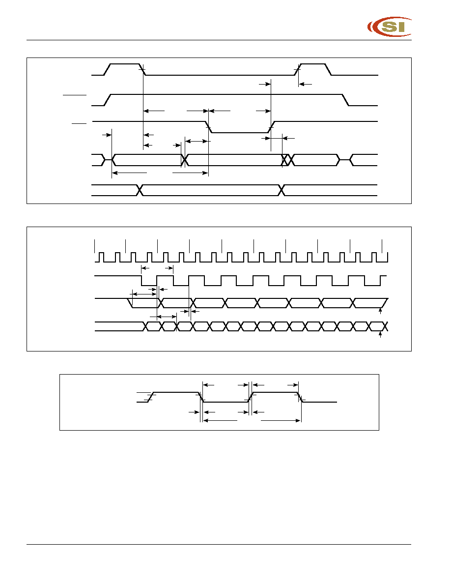
IC80C52
IC80C32
46
Integrated Circuit Solution Inc.
MC002-0B
Figure 34. External Data Memory Write Cycle
Figure 35. Shift Register Mode Timing Waveform
Figure 36. External Clock Drive Waveform
t
AVLL
A7-A0 FROM RI OR DPL
INSTR IN
A7-A0 FROM PCL
t
AVWL
PSEN
PORT 0
PORT 2
ALE
WR
DATA OUT
A15-A8 FROM DPH
A15-A8 FROM PCH
t
WHLH
t
LLWL
t
LLAX
t
QVWX
t
WHQX
t
WLWH
INSTRUCTION
ALE
CLOCK
DATA
OUT
DATA
IN
t
XLXL
t
XHQX
t
QVXH
t
XHDV
t
XHDX
VALID
VALID
VALID
VALID
VALID
VALID
VALID
VALID
SET TI
SET RI
7
8
6
5
4
3
2
1
0
7
6
5
4
3
2
1
0
0.45V
Vcc -- 0.5V
t
CHCX
t
CLCL
t
CLCH
t
CLCX
t
CHCL
0.7Vcc
0.2Vcc -- 0.1

Integrated Circuit Solution Inc.
47
MC002-0B
IC80C52
IC80C32
Note:
1. AC inputs during testing are driven at VCC ≠ 0.5V for logic "1" and 0.45V for logic "0".
Timing measurements are made at V
IH
min for logic "1" and max for logic "0".
Figure 38. AC Test Point
Vcc - 0.5V
0.45V
0.2Vcc + 0.9V
0.2Vcc - 0.1V
Figure 37. ROM Verification Waveforms
P1.0-P1.7
P2.0-P2.3
DATA OUT
ADDRESS
PORT 0
P2.7
t
EHQZ
t
ELQV
t
AVQV

IC80C52
IC80C32
48
Integrated Circuit Solution Inc.
MC002-0B
ORDERING INFORMATION
Commercial Temperature: 0∞C to +70∞C
Speed
Order Part Number
Package
12 MHz
IC80C52-12PL
PLCC
IC80C52-12PQ
PQFP
IC80C52-12W
600mil DIP
24 MHz
IC80C52-24PL
PLCC
IC80C52-24PQ
PQFP
IC80C52-24W
600mil DIP
40 MHz
IC80C52-40PL
PLCC
IC80C52-40PQ
PQFP
IC80C52-40W
600mil DIP
12MHz
IC80C32-12PL
PLCC
IC80C32-12PQ
PQFP
IC80C32-12W
600mil DIP
24MHz
IC80C32-24PL
PLCC
IC80C32-24PQ
PQFP
IC80C32-24W
600mil DIP
40MHz
IC80C32-40PL
PLCC
IC80C32-40PQ
PQFP
IC80C32-40W
600mil DIP
Integrated Circuit Solution Inc.
HEADQUARTER:
NO.2, TECHNOLOGY RD. V, SCIENCE-BASED INDUSTRIAL PARK,
HSIN-CHU, TAIWAN, R.O.C.
TEL: 886-3-5780333
Fax: 886-3-5783000
BRANCH OFFICE:
7F, NO. 106, SEC. 1, HSIN-TAI 5
TH
ROAD,
HSICHIH TAIPEI COUNTY, TAIWAN, R.O.C.
TEL: 886-2-26962140
FAX: 886-2-26962252
http://www.icsi.com.tw