Integrated Circuit Solution Inc.
1
MC003-0B
IC80C54
IC80C58
ICSI reserves the right to make changes to its products at any time without notice in order to improve design and supply the best possible product. We assume no responsibility for any errors
which may appear in this publication. © Copyright 2000, Integrated Circuit Solution Inc.
IC80C54
IC80C58
CMOS SINGLE CHIP
8-BIT MICROCONTROLLER
FEATURES
∑ 80C52 based architecture
∑ 16K x 8 ROM (80C54)
32K x 8 ROM (80C58)
∑ 256 x 8 RAM
∑ Three 16-bit Timer/Counters
∑ Full duplex serial channel
∑ Boolean processor
∑ Four 8-bit I/O ports, 32 I/O lines
∑ Memory addressing capability
≠ 64K ROM and 64K RAM
∑ Program memory lock
≠ Lock bits (2)
∑ Power save modes:
≠ Idle and power-down
∑ Eight interrupt sources
∑ Most instructions execute in 0.3 µs
∑ CMOS and TTL compatible
∑ Maximum speed: 40 MHz @ Vcc = 5V
∑ Packages available:
≠ 40-pin DIP
≠ 44-pin PLCC
≠ 44-pin PQFP
GENERAL DESCRIPTION
The
ICSI
IC80C54 and IC80C58 are high-performance
microcontroller fabricated using high-density CMOS
technology. The CMOS IC80C54/58 is functionally
compatible with the industry standard 80C52/32
microcontrollers.
The IC80C54/58 is designed with 16K x 8 ROM (IC80C54
)and 32Kx8 ROM (IC80C58); 256 x 8 RAM; 32
programmable I/O lines; a serial I/O port for either
multiprocessor communications, I/O expansion or full duplex
UART; three 16-bit timer/counters; an eight-source, two-
priority-level, nested interrupt structure; and an on-chip
oscillator and clock circuit. The IC80C54/58 can be
expanded using standard TTL compatible memory.
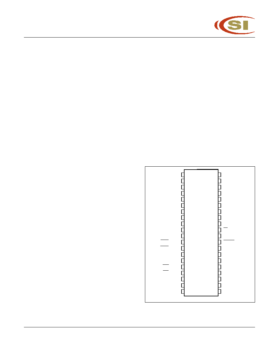
Figure 1. IC80C54/58 Pin Configuration: 40-pin DIP
1
2
3
4
5
6
7
8
9
10
11
12
13
14
15
16
17
18
19
20
40
39
38
37
36
35
34
33
32
31
30
29
28
27
26
25
24
23
22
21
T2/P1.0
T2EX/P1.1
P1.2
P1.3
P1.4
P1.5
P1.6
P1.7
RST
RxD/P3.0
TxD/P3.1
INT0/P3.2
INT1/P3.3
T0/P3.4
T1/P3.5
WR/P3.6
RD/P3.7
XTAL2
XTAL1
GND
V
CC
P0.0/AD0
P0.1/AD1
P0.2/AD2
P0.3/AD3
P0.4/AD4
P0.5/AD5
P0.6/AD6
P0.7/AD7
EA
ALE
PSEN
P2.7/A15
P2.6/A14
P2.5/A13
P2.4/A12
P2.3/A11
P2.2/A10
P2.1/A9
P2.0/A8

IC80C54
IC80C58
2
Integrated Circuit Solution Inc.
MC003-0B
TOP VIEW
Figure 2. IC80C54/58 Pin Configuration: 44-pin PLCC
WR/P3.6
RD/P3.7
XTAL2
XTAL1
GND
NC
A8/P2.0
A9/P2.1
A10/P2.2
A11/P2.3
A12/P2.4
P1.4
P1.3
P1.2
P1.1/T2EX
P1.0/T2
NC
V
CC
P0.0/AD0
P0.1/AD1
P0.2/AD2
P0.3/AD3
P0.4/AD4
P0.5/AD5
P0.6/AD6
P0.7/AD7
EA
NC
ALE
PSEN
P2.7/A15
P2.6/A14
P2.5/A13
P1.5
P1.6
P1.7
RST
RxD/P3.0
NC
TxD/P3.1
INT0/P3.2
INT1/P3.3
T0/P3.4
T1/P3.5
7
8
9
10
11
12
13
14
15
16
17
39
38
37
36
35
34
33
32
31
30
29
INDEX
4
3
6
5
2
1
44
18
19
20
21
22
23
24
43
42
41
40
25
26
27
28

Integrated Circuit Solution Inc.
3
MC003-0B
IC80C54
IC80C58
Figure 3. IC80C54/58 Pin Configuration: 44-pin PQFP
WR/P3.6
RD/P3.7
XTAL2
XTAL1
GND
NC
A8/P2.0
A9/P2.1
A10/P2.2
A11/P2.3
A12/P2.4
P1.4
P1.3
P1.2
P1.1/T2EX
P1.0/T2
NC
V
CC
P0.0/AD0
P0.1/AD1
P0.2/AD2
P0.3/AD3
P0.4/AD4
P0.5/AD5
P0.6/AD6
P0.7/AD7
EA
NC
ALE
PSEN
P2.7/A15
P2.6/A14
P2.5/A13
P1.5
P1.6
P1.7
RST
RxD/P3.0
NC
TxD/P3.1
INT0/P3.2
INT1/P3.3
T0/P3.4
T1/P3.5
1
2
3
4
5
6
7
8
9
10
11
33
32
31
30
29
28
27
26
25
24
23
38
12
13
14
15
16
17
18
37
36
35
34
44
43
42
41
40
39
19
20
21
22
IC80C54
IC80C58
4
Integrated Circuit Solution Inc.
MC003-0B
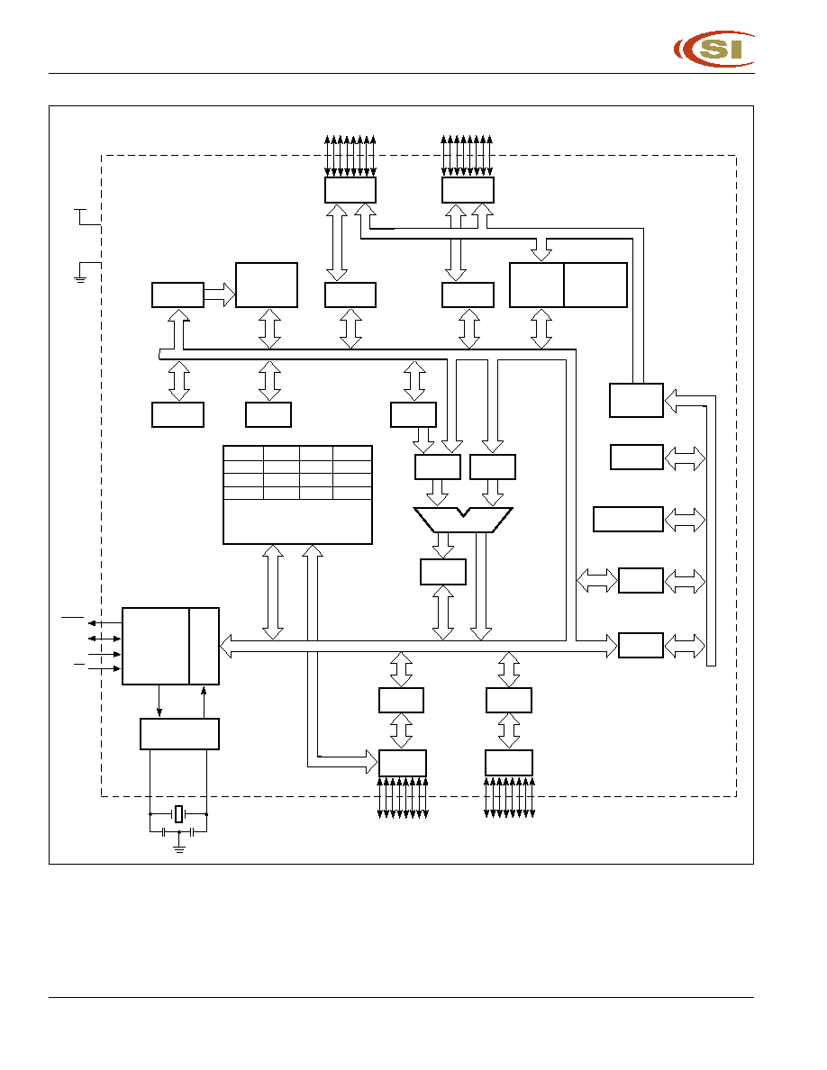
Figure 4. IC80C54/58 Block Diagram
PCON
SCON
TMOD
TCON
T2CON
TH0
TL0
TH1
TL1
TH2
TL2
RCAP2H
RCAP2L SBUF
IE
IP
INTERRUPT
SERIAL PORT
AND TIMER BLOCK
P3
DRIVERS
P3
LATCH
PSW
TIMING
AND
CONTROL
OSCILLATOR
XTAL2
PD
XTAL1
INSTRUCTION
REGISTER
P3.0-P3.7
P1
DRIVERS
P1
LATCH
DPTR
BUFFER
PC
INCREMENTER
PROGRAM
COUNTER
PROGRAM
ADDRESS
REGISTER
P1.0-P1.7
P2.0-P2.7
P0.0-P0.7
PSEN
ALE
RST
EA
TMP2
ALU
ACC
STACK
POINT
B
REGISTER
V
CC
GND
RAM ADDR
REGISTER
P2
LATCH
P0
LATCH
P2
DRIVERS
P0
DRIVERS
ADDRESS
DECODER
& 256
BYTES RAM
ADDRESS
DECODER
& 16/32K
ROM
2 LOCK BITS
TMP1

Integrated Circuit Solution Inc.
5
MC003-0B
IC80C54
IC80C58
Table 1. Detailed Pin Description
Symbol
PDIP
PLCC
PQFP
I/O
Name and Function
ALE
30
33
27
I/O
Address Latch Enable: Output pulse for latching the low byte
of the address during an access to the external memory. In
normal operation, ALE is emitted at a constant rate of 1/6 the
oscillator frequency, and can be used for external timing or
clocking. Note that one ALE pulse is skipped during each
access to external data memory.
EA
31
35
29
I
External Access enable:
EA must be externally held low to
enable the device to fetch code from external program memory
locations 0000H to FFFFH. If
EA is held high, the device
executes from internal program memory unless the program
counter contains an address greater than internal ROM seze.
P0.0-P0.7
39-32
43-36
37-30
I/O
Port 0: Port 0 is an 8-bit open-drain, bidirectional I/O port. Port
0 pins that have 1s written to them float and can be used as high-
impedance inputs. Port 0 is also the multiplexed low-order
address and data bus during accesses to external program and
data memory. In this application, it uses strong internal pullups
when emitting 1s.
P1.0-P1.7
1-8
2-9
40-44
I/O
Port 1: Port 1 is an 8-bit bidirectional I/O port with internal
1-3
pullups. Port 1 pins that have 1s written to them are pulled high
by the internal pullups and can be used as inputs. As inputs, Port
1 pins that are externally pulled low will source current because
of the internal pullups. (See DC Characteristics: I
IL
). The Port 1
output buffers can sink/source four TTL inputs.
Port 1 also receives the low-order address byte during verification.
1
2
40
I
T2(P1.0): Timer/Counter 2 external count input.
2
3
41
I
T2EX(P1.1): Timer/Counter 2 trigger input.
P2.0-P2.7
21-28
24-31
18-25
I/O
Port 2: Port 2 is an 8-bit bidirectional I/O port with internal
pullups. Port 2 pins that have 1s written to them are pulled high
by the internal pullups and can be used as inputs. As inputs, Port
2 pins that are externally pulled low will source current because
of the internal pullups. (See DC Characteristics: I
IL
). Port 2 emits
the high order address byte during fetches from external pro-
gram memory and during accesses to external data memory
that used 16-bit addresses (MOVX @ DPTR). In this application,
Port 2 uses strong internal pullups when emitting 1s. During
accesses to external data memory that use 8-bit addresses
(MOVX @ Ri [i = 0, 1]), Port 2 emits the contents of the P2
Special Function Register.
Port 2 also receives the high-order bits and some control signals
during verification.

IC80C54
IC80C58
6
Integrated Circuit Solution Inc.
MC003-0B
Symbol
PDIP
PLCC
PQFP
I/O
Name and Function
P3.0-P3.7
10-17
11, 13-19
5, 7-13
I/O
Port 3: Port 3 is an 8-bit bidirectional I/O port with internal
pullups. Port 3 pins that have 1s written to them are pulled high
by the internal pullups and can be used as inputs. As inputs, Port
3 pins that are externally pulled low will source current because
of the internal pullups. (See DC Characteristics: I
IL
).
Port 3 also serves the special features of the IC80C54/58, as
listed below:
10
11
5
I
RxD (P3.0): Serial input port.
11
13
7
O
TxD (P3.1): Serial output port.
12
14
8
I
INT0
INT0
INT0
INT0
INT0 (P3.2): External interrupt 0.
13
15
9
I
INT1
INT1
INT1
INT1
INT1 (P3.3): External interrupt 1.
14
16
10
I
T0 (P3.4): Timer 0 external input.
15
17
11
I
T1 (P3.5): Timer 1 external input.
16
18
12
O
WR
WR
WR
WR
WR (P3.6): External data memory write strobe.
17
19
13
O
RD
RD
RD
RD
RD (P3.7): External data memory read strobe.
PSEN
29
32
26
O
Program Store Enable: The read strobe to external program
memory. When the device is executing code from the external
program memory,
PSEN is activated twice each machine cycle
except that two
PSEN activations are skipped during each
access to external data memory.
PSEN is not activated during
fetches from internal program memory.
RST
9
10
4
I
Reset: A high on this pin for two machine cycles while the
oscillator is running, resets the device. An internal MOS resistor
to GND permits a power-on reset using only an external capaci-
tor connected to Vcc.
XTAL 1
19
21
15
I
Crystal 1: Input to the inverting oscillator amplifier and input
to the internal clock generator circuits.
XTAL 2
18
20
14
O
Crystal 2: Output from the inverting oscillator amplifier.
GND
20
22
16
I
Ground: 0V reference.
Vcc
40
44
38
I
Power Supply: This is the power supply voltage for operation.
Table 1. Detailed Pin Description (continued)
OPERATING DESCRIPTION
The detail description of the IC80C54/58 included in this description are:
∑ Memory Map and Registers
∑ The Timer/Counters
∑ The Serial Interface
∑ The Interrupt System
∑ Information
∑ Another information
The detail information desription of the IC80C54/58 refer to IC80C52/32 date sheet
Integrated Circuit Solution Inc.
7
MC003-0B
IC80C54
IC80C58
Table 2. Reset Values of the SFR's
SFR Name
Reset Value
PC
0000H
ACC
00H
B
00H
PSW
00H
SP
07H
DPTR
0000H
P0-P3
FFH
IP
XX000000B
IE
0X000000B
TMOD
00H
TCON
00H
T2CON
00H
TH0
00H
TL0
00H
TH1
00H
TL1
00H
TH2
00H
TL2
00H
RCAP2H
00H
RCAP2L
00H
SCON
00H
SBUF
Indeterminate
PCON
0XXX0000B
OTHER INFORMATION
Reset
The reset input is the RST pin, which is the input to a
Schmitt Trigger.
A reset is accomplished by holding the RST pin high for at
least two machine cycles (24 oscillator periods), while the
oscillator is running. The CPU responds by generating an
internal reset, with the timing shown in Figure 7.
The external reset signal is asynchronous to the internal
clock. The RST pin is sampled during State 5 Phase 2 of
every machine cycle. The port pins will maintain their
current activities for 19 oscillator periods after a logic 1 has
been sampled at the RST pin; that is, for 19 to 31 oscillator
periods after the external reset signal has been applied to
the RST pin.
The internal reset algorithm writes 0s to all the SFRs except
the port latches, the Stack Pointer, and SBUF. The port
latches are initialized to FFH, the Stack Pointer to 07H, and
SBUF is indeterminate. Table 9 lists the SFRs and their
reset values.
Then internal RAM is not affected by reset. On power-up
the RAM content is indeterminate.

IC80C54
IC80C58
8
Integrated Circuit Solution Inc.
MC003-0B
Power-on Reset
An automatic reset can be obtained when V
CC
goes through
a 10 µF capacitor and GND through an 8.2K resistor,
providing the Vcc rise time does not exceed 1 msec and the
oscillator start-up time does not exceed 10 msec. This
Power-on reset circuit is shown if Figure 21. The CMOS
devices do not require the 8.2K pulldown resistor, although
its presence does no harm.
When power is turned on, the circuit holds the RST pin high
for an amount of time that depends on the value of the
capacitor and the rate at which it charges. To ensure a good
reset, the RST pin must be high long enough to allow the
oscillator time to start-up (normally a few msec) plus two
machine cycles.
Note that the port pins will be in a random state until the
oscillator has start and the internal reset algorithm has
written 1s to them.
With this circuit, reducing V
CC
quickly to 0 causes the RST
pin voltage to momentarily fall below 0V. However, this
voltage is internally limited and will not harm the device.
Figure 6. Power-On Reset Circuit
Vcc
RST
GND
Vcc
IC80C54/58
10 F
8.2K
+
-
Figure 7. Reset Timing
12 OSC. PERIODS
ALE
RST
SAMPLE
RST
SAMPLE
RST
INTERNAL RESET SIGNAL
PSEN
P0
11 OSC. PERIODS
INST
ADDR
INST
INST
INST
19 OSC. PERIODS
S5 S6 S1 S2 S3 S4 S5 S6 S1 S2 S3 S4 S5 S6 S1 S2 S3 S4
ADDR
ADDR
ADDR
INST
ADDR
Integrated Circuit Solution Inc.
9
MC003-0B
IC80C54
IC80C58
Power-Saving Modes of Operation
The IC80C54/58 has two power-reducing modes. Idle and
Power-down. The input through which backup power is
supplied during these operations is Vcc. Figure 23 shows
the internal circuitry which implements these features. In
the Idle mode (IDL = 1), the oscillator continues to run and
the Interrupt, Serial Port, and Timer blocks continue to be
clocked, but the clock signal is gated off to the CPU. In
Power-down (PD = 1), the oscillator is frozen. The Idle and
Power-down modes are activated by setting bits in Special
Function Register PCON.
Idle Mode
An instruction that sets PCON.0 is the last instruction
executed before the Idle mode begins. In the Idle mode, the
internal clock signal is gated off to the CPU, but not to the
Interrupt, Timer, and Serial Port functions. The CPU status
is preserved in its entirety; the Stack Pointer, Program
Counter, Program Status Word, Accumulator, and all other
registers maintain their data during Idle. The port pins hold
the logical states they had at the time Idle was activated.
ALE and
PSEN hold at logic high levels.
There are two ways to terminate the Idle. Activation of any
enabled interrupt will cause PCON.0 to be cleared by
hardware, terminating the Idle mode. The interrupt will be
serviced, and following RETI the next instruction to be
executed will be the one following the instruction that put
the device into Idle.
The flag bits GF0 and GF1 can be used to indicate whether
an interrupt occurred during normal operation or during an
Idle. For example, an instruction that activates Idle can also
set one or both flag bits. When Idle is terminated by an
interrupt, the interrupt service routine can examine the flag
bits.
The other way of terminating the Idle mode is with a
hardware reset. Since the clock oscillator is still running,
the hardware reset must be held active for only two
machine cycles (24 oscillator periods) to complete the
reset.
The signal at the RST pin clears the IDL bit directly and
asynchronously. At this time, the CPU resumes program
execution from where it left off; that is, at the instruction
following the one that invoked the Idle Mode. As shown in
Figure 22, two or three machine cycles of program execution
may take place before the internal reset algorithm takes
control. On-chip hardware inhibits access to the internal
RAM during his time, but access to the port pins is not
inhibited. To eliminate the possibility of unexpected outputs
at the port pins, the instruction following the one that
invokes Idle should not write to a port pin or to external data
RAM.
Power-down Mode
An instruction that sets PCON.1 is the last instruction
executed before Power-down mode begins. In the Power-
down mode, the on-chip oscillator stops. With the clock
frozen, all functions are stopped, but the on-chip RAM and
Special function Registers are held. The port pins output
the values held by their respective SFRs. ALE and
PSEN
output lows.
In the Power-down mode of operation, Vcc can be reduced
to as low as 2V. However, Vcc must not be reduced before
the Power-down mode is invoked, and Vcc must be restored
to its normal operating level before the Power-down mode
is terminated. The reset that terminates Power-down also
frees the oscillator. The reset should not be activated
before Vcc is restored to its normal operating level and
must be held active long enough to allow the oscillator to
restart and stabilize (normally less than 10 msec).
The only exit from Power-down is a hardware reset. Reset
redefines all the SFRs but does not change the on-chip
RAM.
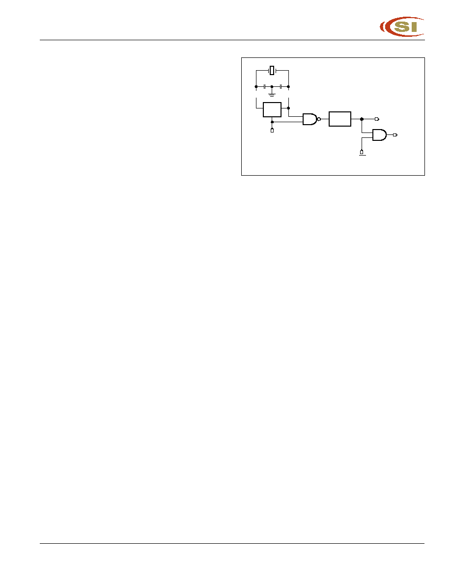
OSC
CLOCK
GEN
PD
XTAL 1
XTAL 2
IDL
CPU
INTERRUPT,
SERIAL PORT,
TIMER BLOCKS
Figure 8. Idle and Power-Down Hardware
IC80C54
IC80C58
10
Integrated Circuit Solution Inc.
MC003-0B
Table 3. Status of the External Pins During Idle and Power-down Modes.
Mode
Memory
ALE
PSEN
PSEN
PSEN
PSEN
PSEN
PORT 0
PORT 1
PORT 2
PORT 3
Idle
Internal
1
1
Data
Data
Data
Data
Idle
External
1
1
Float
Data
Address
Data
Power-down
Internal
0
0
Data
Data
Data
Data
Power-down
External
0
0
Float
Data
Data
Data
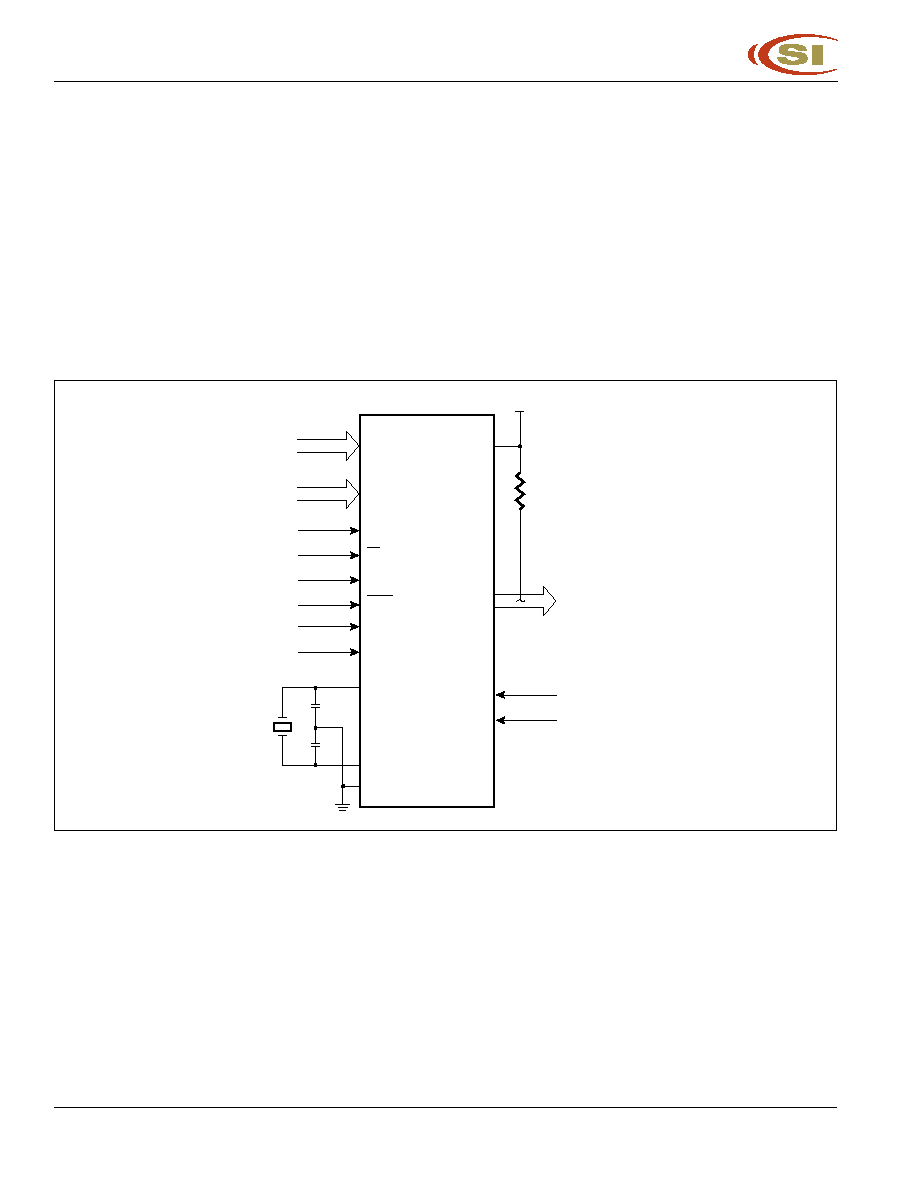
On-Chip Oscillators
The on-chip oscillator circuitry of the IC80C54/58 is a
single stage inverter, intended for use as a crystal-
controlled, positive reactance oscillator. In this application
the crystal is operated in its fundamental response mode
as an inductive reactance in parallel resonance with
capacitance external to the crystal (Figure 9). Examples
of how to drive the clock with external oscillator are shown
in Figure 10.
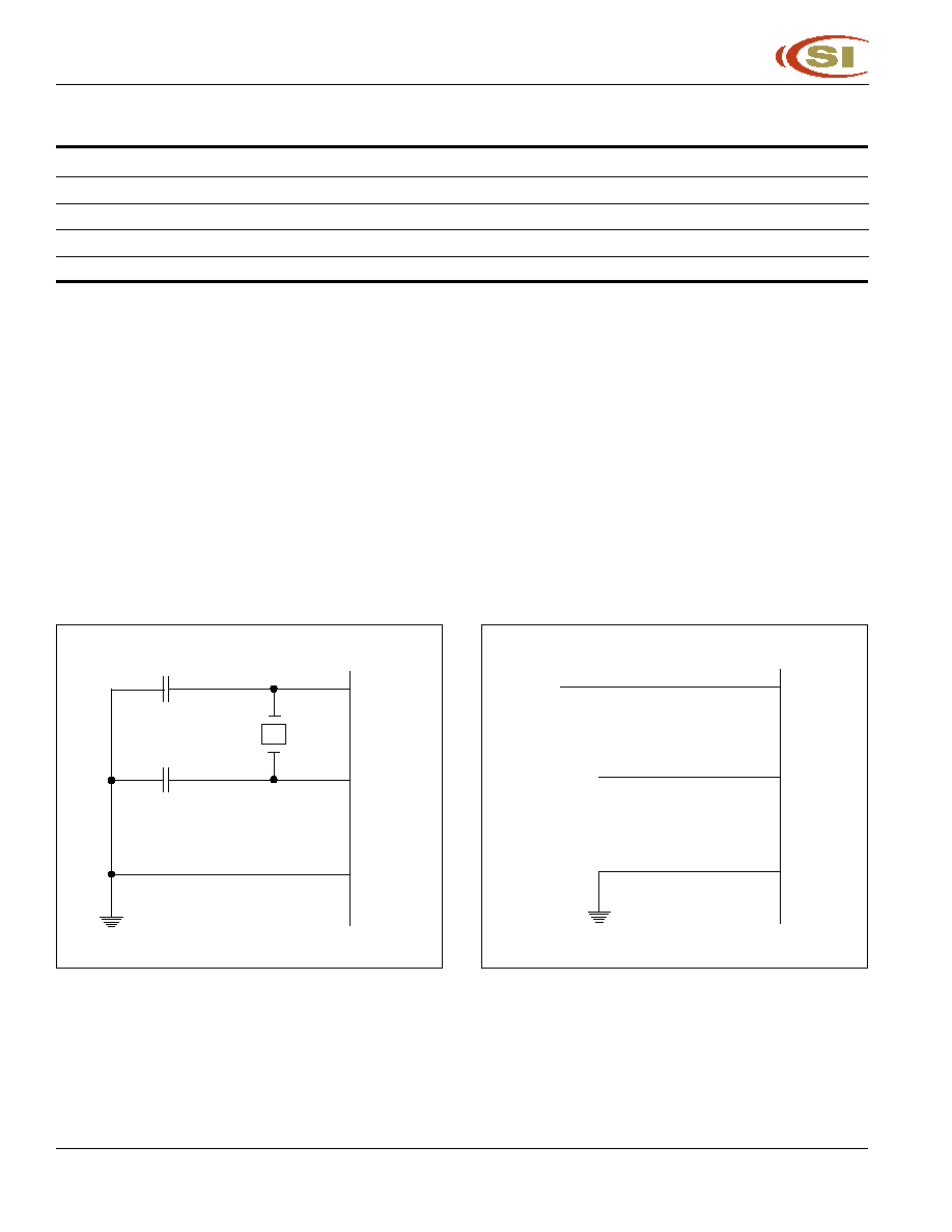
Figure 9. Oscillator Connections
The crystal specifications and capacitance values (C1 and
C2 in Figure 9) are not critical. 20 pF to 30 pF can be used
in these positions at a 12 MHz to 24 MHz frequency with
good quality crystals. (For ranges greater than 24 MHz refer
to Figure 11.) A ceramic resonator can be used in place of
the crystal in cost-sensitive applications. When a ceramic
resonator is used, C1 and C2 are normally selected to be of
somewhat higher values. The manufacturer of the ceramic
resonator should be consulted for recommendation on the
values of these capacitors.
GND
XTAL1
XTAL2
EXTERNAL
OSCILLATOR
SIGNAL
NC
Figure 10. External Clock Drive Configuration
C1
C2
GND
XTAL1
XTAL2
Integrated Circuit Solution Inc.
11
MC003-0B
IC80C54
IC80C58
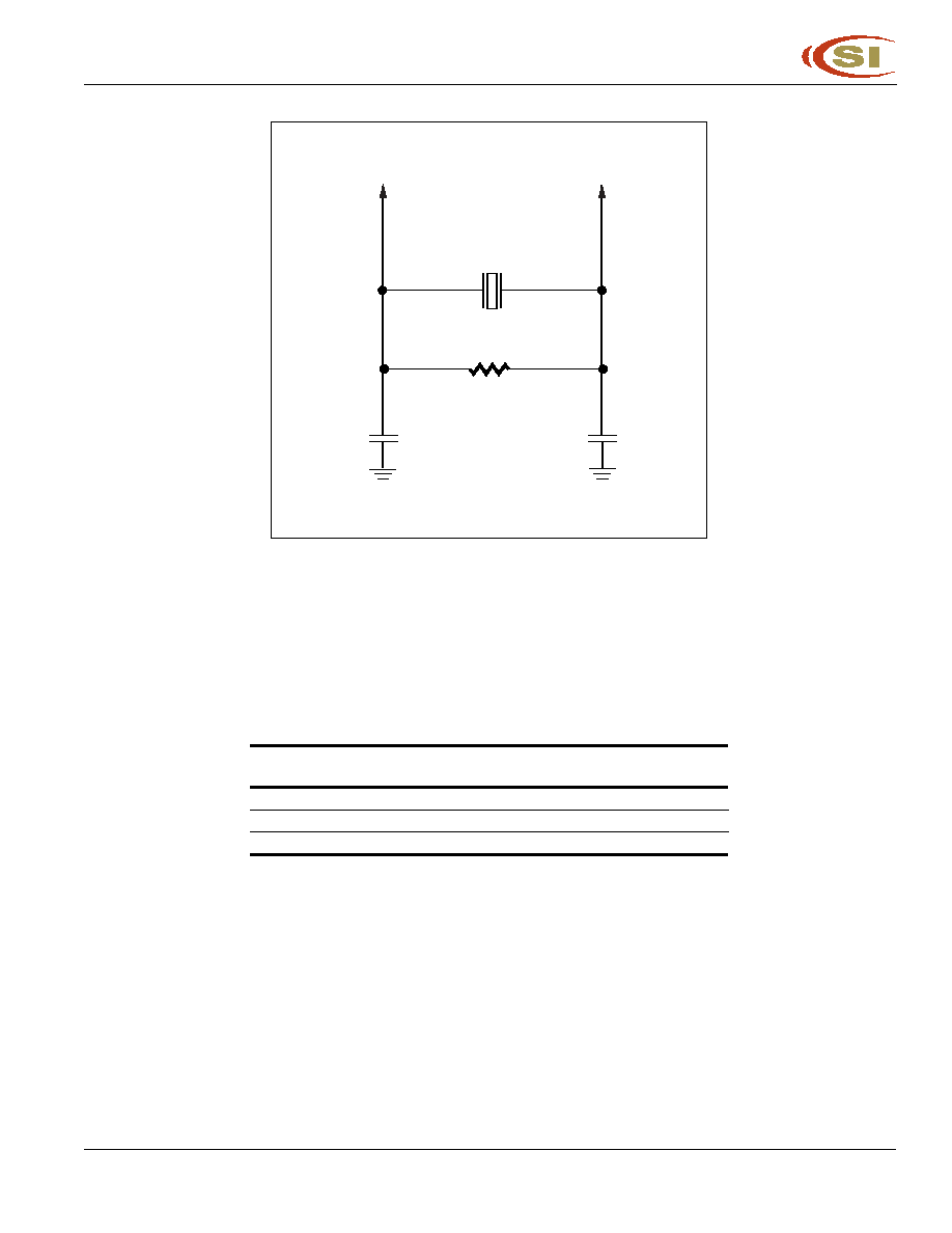
Figure 11. Oscillator Connections for High Speed (> 24 MHz)
Note:
When the frequency is higher than 24 MHz, please refer to Table 4 for recommended values of C1, C2, and R.
XTAL2
XTAL1
C1
C2
R
Table 4. Recommended Value for C1, C2, R
Frequency Range
3.5 MHz - 24 MHz
24 MHz - 40 MHz
C1
20 pF-30 pF
3 pF-10 pF
C2
20 pF-30 pF
3 pF-10 pF
R
Not Apply
6.2K-10K
IC80C54
IC80C58
12
Integrated Circuit Solution Inc.
MC003-0B
ROM Verification
The address of the program menory location to be read is
applied to Port 1 and pins P2.5-P2.0 (A14 is P3.4 for
IC80C58). The other pins should be held at the "Verify"
level are indicated in Figure 12. The contents of the ad-
dressed locations exits on Port 0. External pullups are re-
quired on Rort 0 for this operation. Figure 12 shows the
setup to verify the program memory.
Figure 12. ROM Verification
XTAL2
GND
XTAL1
4-6 MHz
P1
P2.4-P2.0
RST
EA
ALE
PSEN
P2.7
P2.6
P2.5
P3.4
A13
P14
IC80C54 : A13 - A0
IC80C58 : A14 - A0
1
1
1
0
0
0
Vcc
P0
+ 5V
A7-A0
A12-A8
PGM
DATA
10K x 8

Integrated Circuit Solution Inc.
13
MC003-0B
IC80C54
IC80C58
ROM Lock System
The ICSI 80C54/58 contains two Program Memory Locking:
Security Bit 1:
When programmed, this bit two effects on masked ROM
parts:
1) External MOVC is disable, and
2) EA pin is latch on reset.
Security Bit2:
When programmed, this bit inhibits Verify User ROM.
OPERATING RANGE
(1)
Range
Ambient Temperature
V
CC
Oscillator Frequency
Commercial
0∞C to +70∞C
5V ± 10%
3.5 to 40 MHz
Note:
1. Operating ranges define those limits between which the functionality of the device is guaranteed.
ABSOLUTE MAXIMUM RATINGS
(1)
Symbol
Parameter
Value
Unit
V
TERM
Terminal Voltage with Respect to GND
(2)
≠2.0 to +7.0
V
T
BIAS
Temperature Under Bias
(3)
0 to +70
∞C
T
STG
Storage Temperature
≠65 to +125
∞C
P
T
Power Dissipation
1.5
W
Note:
1. Stress greater than those listed under ABSOLUTE MAXIMUM RATINGS may cause
permanent damage to the device. This is a stress rating only and functional operation
of the device at these or any other conditions above those indicated in the operational
sections of this specification is not implied. Exposure to absolute maximum rating
conditions for extended periods may affect reliability.
2. Minimum DC input voltage is ≠0.5V. During transitions, inputs may undershoot to ≠2.
0V for periods less than 20 ns. Maximum DC voltage on output pins is Vcc + 0.5V
which may overshoot to Vcc + 2.0V for periods less than 20 ns.
3. Operating temperature is for commercial products only defined by this specification.

IC80C54
IC80C58
14
Integrated Circuit Solution Inc.
MC003-0B
DC CHARACTERISTICS
(Ta=0∞C to 70 ∞C; VCC=5V+10%; VSS=0V )
Symbol
Parameter
Test conditions
Min
Max
Unit
V
IL
Input low voltage (All except
EA)
≠0.5
0.2Vcc ≠ 0.1
V
V
IL
1
Input low voltage (
EA)
≠0.5
0.2Vcc ≠ 0.3
V
V
IH
Input high voltage
0.2Vcc + 0.9
Vcc + 0.5
V
(All except XTAL 1, RST)
V
IH
1
Input high voltage (XTAL 1)
0.7Vcc
Vcc + 0.5
V
V
SCH
+
RST positive schmitt-trigger
0.7Vcc
Vcc + 0.5
V
threshold voltage
V
SCH
≠
RST negative schmitt-trigger
0
0.3Vcc
V
threshold voltage
V
OL
(1)
Output low voltage
Iol = 100 µA
--
0.3
V
(Ports 1, 2, 3)
I
OL
= 1.6 mA
--
0.45
V
I
OL
= 3.5 mA
--
1.0
V
V
OL
1
(1)
Output low voltage
I
OL
= 200 µA
--
0.3
V
(Port 0, ALE,
PSEN)
I
OL
= 3.2 mA
--
0.45
V
I
OL
= 7.0 mA
--
1.0
V
V
OH
Output high voltage
I
OH
= ≠10 µA
0.9Vcc
--
V
(Ports 1, 2, 3, ALE,
PSEN)
Vcc = 4.5V-5.5V
I
OL
= ≠25 µA
0.75Vcc
--
V
I
OL
= ≠60 µA
2.4
--
V
V
OH
1
Output high voltage
I
OH
= ≠80 µA
0.9Vcc
--
V
(Port 0, ALE,
PSEN)
Vcc = 4.5V-5.5V
I
OH
= ≠300 µA
0.75Vcc
--
V
I
OH
= ≠800 µA
2.4
--
V
I
IL
Logical 0 input current (Ports 1, 2, 3) V
IN
= 0.45V
--
≠50
µA
I
LI
Input leakage current (Port 0)
0.45V < V
IN
< Vcc
≠10
+10
µA
I
TL
Logical 1-to-0 transition current
V
IN
= 2.0V
--
≠650
µA
(Ports 1, 2, 3)
R
RST
RST pulldown resister
50
300
K
Note:
1. Under steady state (non-transient) conditions, I
OL
must be externally limited as follows:
Maximum I
OL
per port pin:
10 mA
Maximum I
OL
per 8-bit port
Port 0: 26 mA
Ports 1, 2, 3: 15 mA
Maximum total I
OL
for all output pins: 71 mA
If I
OL
exceeds the test condition, V
OL
may exceed the related specification.
Integrated Circuit Solution Inc.
15
MC003-0B
IC80C54
IC80C58
POWER SUPPLY CHARACTERISTICS
Symbol
Parameter
Test conditions
Min
Max
Unit
Icc
Power supply current
(1)
Vcc = 5.0V
Active mode
12 MHz
--
20
mA
16 MHz
--
26
mA
20 MHz
--
32
mA
25 MHz
--
38
mA
36 MHz
--
50
mA
40 MHz
--
62
mA
Idle mode
12 MHz
--
5
mA
16 MHz
--
6
mA
20 MHz
--
7.6
mA
25 MHz
--
9
mA
36 MHz
--
12
mA
40 MHz
--
15
mA
Power-down mode
V
CC
= 5V
--
100
µA
Note:
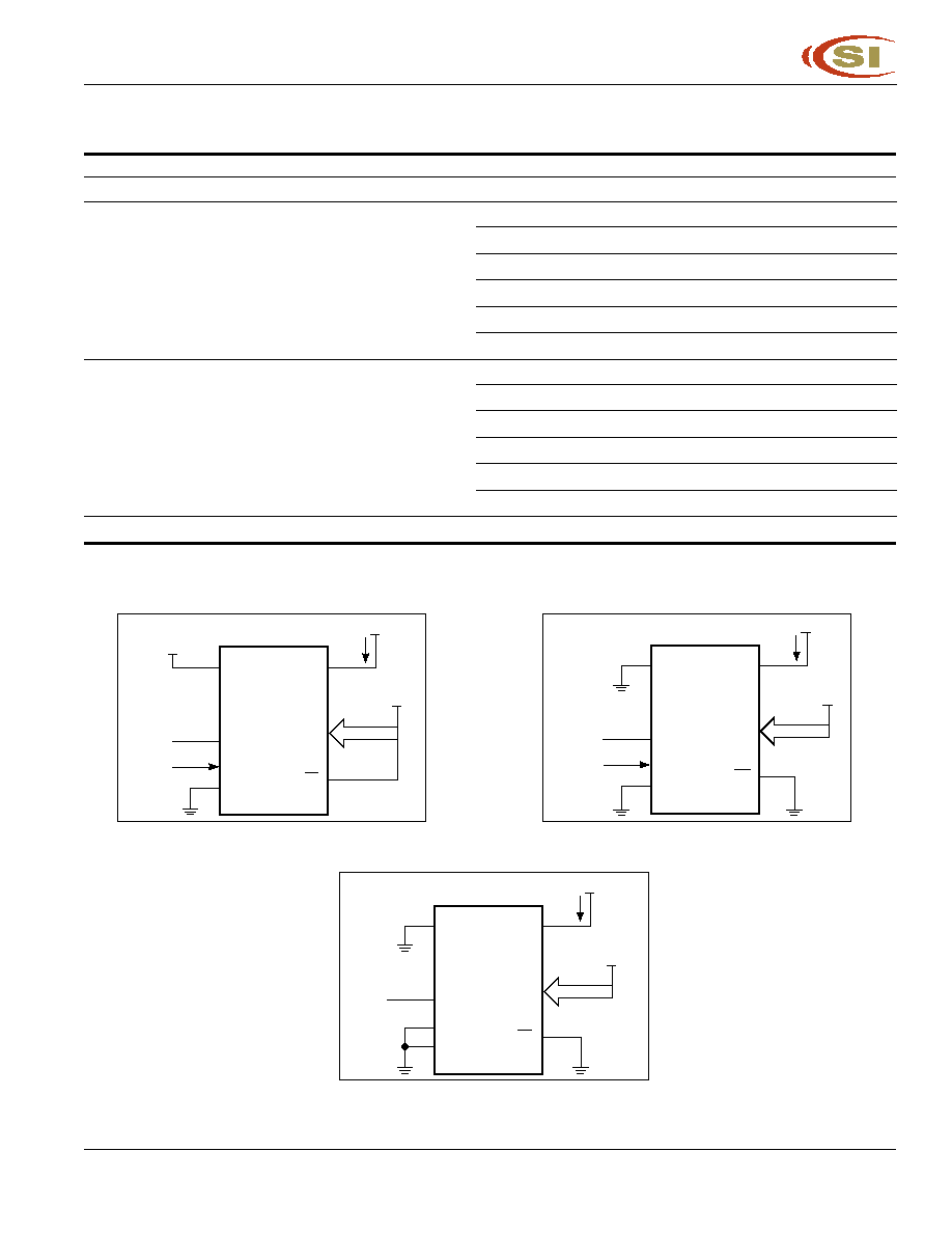
1. See Figures13,14,15, and 16 for Icc test conditiions.
Figure 13. Active Mode
Figure 14. Idle Mode
Figure 15. Power-down Mode
XTAL1
GND
NC
RST
Vcc
P0
EA
Vcc
Vcc
CLOCK
SIGNAL
Icc
XTAL2
Vcc
XTAL1
GND
NC
RST
Vcc
P0
EA
Vcc
Vcc
CLOCK
SIGNAL
Icc
XTAL2
XTAL1
GND
NC
RST
Vcc
P0
EA
Vcc
Vcc
Icc
XTAL2

IC80C54
IC80C58
16
Integrated Circuit Solution Inc.
MC003-0B
Figure 16. Clock Signal Waveform for I
CC
Tests in Active and Idle Mode (t
CLCH
=t
CHCL
=5 ns)
EXTERNAL MEMORY CHARACTERISTICS
24 MHz
40 MHz
Variable Oscillator
Clock
Clock
(3.5 - 40 MHz)
Symbol
Parameter
Min
Max
Min Max
Min
Max
Unit
1/t
CLCL
Oscillator frequency
--
--
--
--
3.5
40
MHz
t
LHLL
ALE pulse width
68
--
35
--
2t
CLCL
≠15
--
ns
t
AVLL
Address valid to ALE low
26
--
10
--
t
CLCL
≠15
--
ns
t
LLAX
Address hold after ALE low
31
--
15
--
t
CLCL
≠10
--
ns
t
LLIV
ALE low to valid instr in
--
147
--
80
--
4t
CLCL
≠20
ns
t
LLPL
ALE low to
PSEN low
31
--
15
--
t
CLCL
≠10
--
ns
t
PLPH
PSEN pulse width
110
--
60
--
3t
CLCL
≠15
--
ns
t
PLIV
PSEN low to valid instr in
--
105
--
55
--
3t
CLCL
≠20
ns
t
PXIX
Input instr hold after
PSEN
0
--
0
--
0
--
ns
t
PXIZ
Input instr float after
PSEN
--
37
--
20
--
t
CLCL
≠5
ns
t
AVIV
Address to valid instr in
--
188
--
105
--
5t
CLCL
≠20
ns
t
PLAZ
PSEN low to address float
--
10
--
10
--
10
ns
t
RLRH
RD pulse width
230
--
130
--
6t
CLCL
≠20
--
ns
t
WLWH
WR pulse width
230
--
130
--
6t
CLCL
≠20
--
ns
t
RLDV
RD low to valid data in
--
157
--
90
--
4t
CLCL
≠10
ns
t
RHDX
Data hold after
RD
0
--
0
--
0
--
ns
t
RHDZ
Data float after
RD
--
78
--
45
--
2t
CLCL
≠5
ns
t
LLDV
ALE low to valid data in
--
282
--
165
--
7t
CLCL
≠10
ns
t
AVDV
Address to valid data in
--
323
--
190
--
8t
CLCL
≠10
ns
t
LLWL
ALE low to
RD or WR low
105
145
55
95
3t
CLCL
≠20
3t
CLCL
+20
ns
t
AVWL
Address to
RD or WR low
146
--
80
--
4t
CLCL
≠20
--
ns
t
QVWX
Data valid to
WR transition
26
--
10
--
t
CLCL
≠15
--
ns
t
WHQX
Data hold after
WR
31
--
15
--
t
CLCL
≠10
--
ns
t
RLAZ
RD low to address float
--
0
--
0
--
0
ns
t
WHLH
RD or WR high to ALE high
26
57
10
40
t
CLCL
≠15
t
CLCL
+15
ns
0.45V
Vcc -- 0.5V
t
CHCX
t
CLCL
t
CLCH
t
CLCX
t
CHCL
0.7Vcc
0.2Vcc -- 0.1
Integrated Circuit Solution Inc.
17
MC003-0B
IC80C54
IC80C58
EXTERNAL MEMORY CHARACTERISTICS
24 MHz
40 MHz
Variable Oscillator
Clock
Clock
(3.5-40 MHz)
Symbol
Parameter
Min
Max
Min Max
Min
Max
Unit
t
XLXL
Serial port clock cycle time
490
510
290 310
12t
CLCL
≠10
12t
CLCL
+10
ns
t
QVXH
Output data setup to
406
--
240
--
10t
CLCL
≠10
--
ns
clock rising edge
t
XHQX
Output data hold after
73
--
40
--
2t
CLCL
≠10
--
ns
clock rising edge
t
XHDX
Input data hold after
0
--
0
--
0
--
ns
clock rising edge
t
XHDV
Clock rising edge to
--
417
--
250
--
10t
CLCL
ns
input data valid
EXTERNAL CLOCK DRIVE
Symbol
Parameter
Min
Max
Unit
1/t
CLCL
Oscillator Frequency
3.5
40
MHz
t
CHCX
High time
10
--
ns
t
CLCX
Low time
10
--
ns
t
CLCH
Rise time
--
10
ns
t
CHCL
Fall time
--
10
ns
ROM VERIFICATION CHARACTERISTICS
Symbol
Parameter
Min
Max
Unit
1/t
CLCL
Oscillator Frequency
4
6
MHz
t
AVQV
Address to data valid
--
40t
CLCL
t
ELQV
ENABLE low to data valid
--
48t
CLCL
t
EHQZ
Data float after ENABLE
0
48t
CLCL

IC80C54
IC80C58
18
Integrated Circuit Solution Inc.
MC003-0B
Figure 17. External Program Memory Read Cycle
Figure 18. External Data Memory Read Cycle
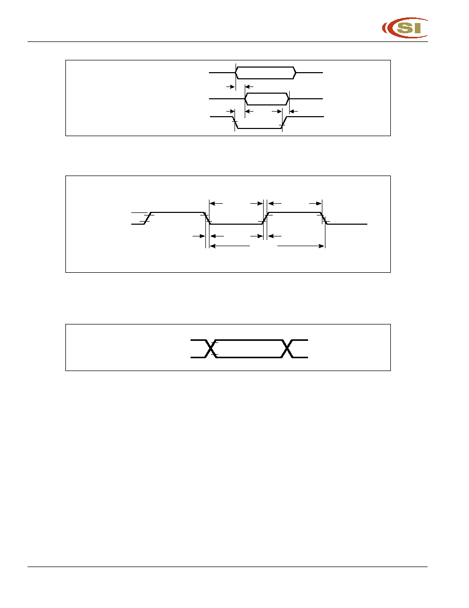
TIMING WAVEFORMS
t
LHLL
ALE
t
AVLL
t
LLPL
t
PLPH
t
PLIV
t
LLAX
t
PLAZ
t
PXIZ
t
PXIX
A7-A0
INSTR IN
A7-A0
t
LLIV
t
AVIV
PSEN
PORT 0
PORT 2
A15-A8
A15-A8
t
LLDV
t
AVLL
A7-A0 FROM RI OR DPL
INSTR IN
A7-A0 FROM PCL
t
AVWL
t
AVDV
PSEN
PORT 0
PORT 2
ALE
RD
DATA IN
A15-A8 FROM DPH
A15-A8 FROM PCH
t
WHLH
t
LLWL
t
LLAX
t
RLAZ
t
RLDV
t
RHDZ
t
RHDX
t
RLRH

Integrated Circuit Solution Inc.
19
MC003-0B
IC80C54
IC80C58
Figure 19. External Data Memory Write Cycle
Figure 20. Shift Register Mode Timing Waveform
t
AVLL
A7-A0 FROM RI OR DPL
INSTR IN
A7-A0 FROM PCL
t
AVWL
PSEN
PORT 0
PORT 2
ALE
WR
DATA OUT
A15-A8 FROM DPH
A15-A8 FROM PCH
t
WHLH
t
LLWL
t
LLAX
t
QVWX
t
WHQX
t
WLWH
INSTRUCTION
ALE
CLOCK
DATA
OUT
DATA
IN
t
XLXL
t
XHQX
t
QVXH
t
XHDV
t
XHDX
VALID
VALID
VALID
VALID
VALID
VALID
VALID
VALID
SET TI
SET RI
7
8
6
5
4
3
2
1
0
7
6
5
4
3
2
1
0
IC80C54
IC80C58
20
Integrated Circuit Solution Inc.
MC003-0B
Note:
1. AC inputs during testing are driven at VCC ≠ 0.5V for logic "1" and 0.45V for logic "0".
Timing measurements are made at V
IH
min for logic "1" and max for logic "0".
Figure 23. AC Test Point
Vcc - 0.5V
0.45V
0.2Vcc + 0.9V
0.2Vcc - 0.1V
Figure 22. External Clock Drive Waveforms
Figure 21. ROM Verification Waveforms
P1.0-P1.7
P2.0-P2.5[A14(P3.4)]
DATA OUT
ADDRESS
PORT 0
P2.7
t
EHQZ
t
ELQV
t
AVQV
0.45V
Vcc -- 0.5V
t
CHCX
t
CLCL
t
CLCH
t
CLCX
t
CHCL
0.7Vcc
0.2Vcc -- 0.1

Integrated Circuit Solution Inc.
21
MC003-0B
IC80C54
IC80C58
ORDERING INFORMATION
Commercial Temperature: 0∞C to +70∞C
Speed
Order Part Number
Package
12 MHz
IC80C54/58-12PL
PLCC
IC80C54/58-12PQ
PQFP
IC80C54/58-12W
600mil DIP
24 MHz
IC80C54/58-24PL
PLCC
IC80C54/58-24PQ
PQFP
IC80C54/58-24W
600mil DIP
40 MHz
IC80C54/58-40PL
PLCC
IC80C54/58-40PQ
PQFP
IC80C54/58-40W
600mil DIP
Integrated Circuit Solution Inc.
HEADQUARTER:
NO.2, TECHNOLOGY RD. V, SCIENCE-BASED INDUSTRIAL PARK,
HSIN-CHU, TAIWAN, R.O.C.
TEL: 886-3-5780333
Fax: 886-3-5783000
BRANCH OFFICE:
7F, NO. 106, SEC. 1, HSIN-TAI 5
TH
ROAD,
HSICHIH TAIPEI COUNTY, TAIWAN, R.O.C.
TEL: 886-2-26962140
FAX: 886-2-26962252
http://www.icsi.com.tw

IC80C54
IC80C58
22
Integrated Circuit Solution Inc.
MC003-0B