 | –≠–ª–µ–∫—Ç—Ä–æ–Ω–Ω—ã–π –∫–æ–º–ø–æ–Ω–µ–Ω—Ç: IC89C52A | –°–∫–∞—á–∞—Ç—å:  PDF PDF  ZIP ZIP |
IC89C52(51)A
Integrated C ircuitSolution Inc.
1
MC008-0C 11/27/2001
ICSI reserves the right to make changes to its products at any time without notice in order to improve design and supply the best possible product. We assume no responsibility for any errors
which may appear in this publication. © Copyright 2000, Integrated Circuit Solution Inc.
CMOS SINGLE CHIP
8-BIT MICROCONTROLLER
with 8(4)-Kbytes of FLASH
FEATURES
∑ 80C52(51) based architecture
∑ 8(4)-Kbytes Flash memory with fast-pulse
programming algorithm and software protection
∑ 256 x 8 RAM (128x8 RAM)
∑ Three (Two)16-bit Timer/Counters
∑ Full duplex serial channel
∑ Boolean processor
∑ Four 8-bit I/O ports, 32 I/O lines
∑ Memory addressing capability
≠ 64K ROM and 64K RAM
∑ Program memory lock
≠ Lock bits (3)
∑ Power save modes:
≠ Idle and power-down
∑ Eight interrupt sources
∑ Most instructions execute in 0.3 µs
∑ CMOS and TTL compatible
∑ Maximum speed: 40 MHz @ Vcc = 5V
∑ Packages available:
≠ 40-pin DIP
≠ 44-pin PLCC
≠ 44-pin PQFP
GENERAL DESCRIPTION
The ICSI IC89C52(51)A is a high-performance micro-
controller fabricated with high-density CMOS technology.
The CMOS IC89C52A is functionally compatible with the
NMOS Intel 8052(51), Philips' 80C52(51) micro controller.
The IC89C52(51)A contains a 8K (4K) x 8 Flash; a 256
x 8 RAM (128 x 8 RAM); 32 I/O lines for either multi-
processor communications; I/O expansion or full duplex
UART; three (two) 16-bit timers/counters; a six-source
(five-source), two-priority-level, nested interrupt structure;
and on chip oscillator and clock circuit. The IC89C52(51)
A can be expanded using standard TTL compatible memory.
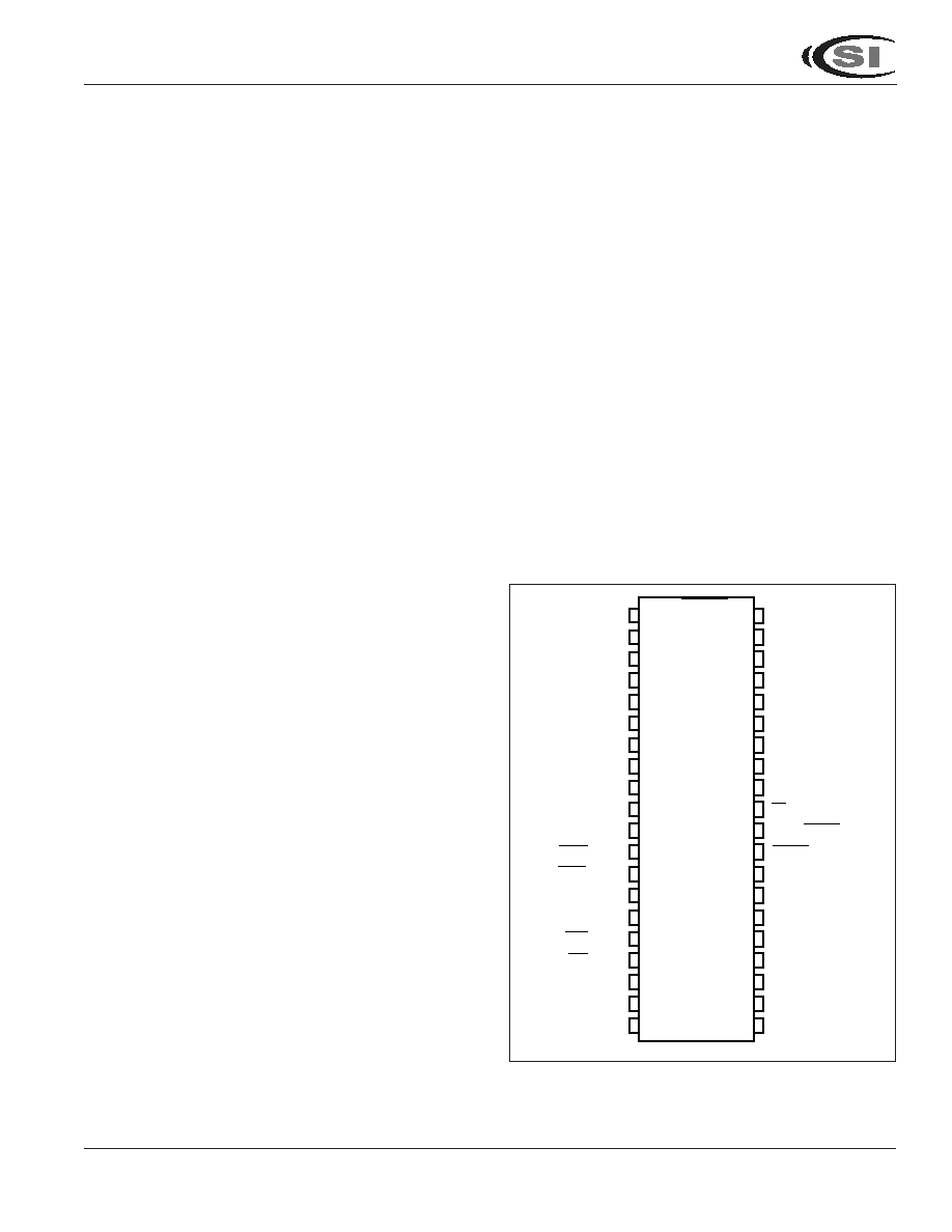
Figure 1. IC89C52(51)A Pin Configuration: 40-pin DIP
1
2
3
4
5
6
7
8
9
10
11
12
13
14
15
16
17
18
19
20
40
39
38
37
36
35
34
33
32
31
30
29
28
27
26
25
24
23
22
21
T2/P1.0
T2EX/P1.1
P1.2
P1.3
P1.4
P1.5
P1.6
P1.7
RST
RxD/P3.0
TxD/P3.1
INT0/P3.2
INT1/P3.3
T0/P3.4
T1/P3.5
WR/P3.6
RD/P3.7
XTAL2
XTAL1
GND
VCC
P0.0/AD0
P0.1/AD1
P0.2/AD2
P0.3/AD3
P0.4/AD4
P0.5/AD5
P0.6/AD6
P0.7/AD7
EA/VPP
ALE/PROG
PSEN
P2.7/A15
P2.6/A14
P2.5/A13
P2.4/A12
P2.3/A11
P2.2/A10
P2.1/A9
P2.0/A8
IC89C52(51)A
2
Integrated C ircuitSolution Inc.
MC008-0C 11/27/2001
TOP VIEW
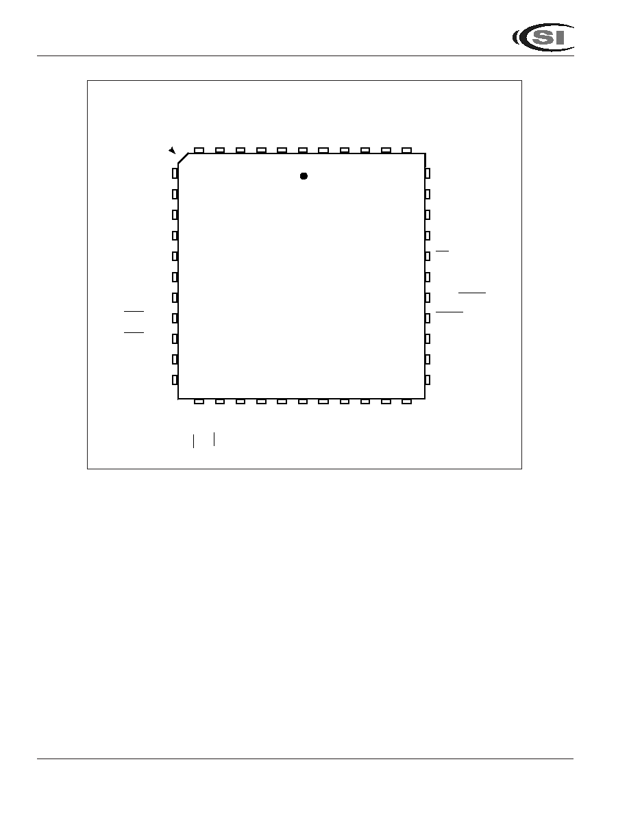
Figure 2. IC89C52(51)A Pin Configuration: 44-pin PLCC
WR/P3.6
RD/P3.7
XTAL2
XTAL1
GND
NC
A8/P2.0
A9/P2.1
A10/P2.2
A11/P2.3
A12/P2.4
P1.4
P1.3
P1.2
P1.1/T2EX
P1.0/T2
NC
VCC
P0.0/AD0
P0.1/AD1
P0.2/AD2
P0.3/AD3
P0.4/AD4
P0.5/AD5
P0.6/AD6
P0.7/AD7
EA/VPP
NC
ALE/PROG
PSEN
P2.7/A15
P2.6/A14
P2.5/A13
P1.5
P1.6
P1.7
RST
RxD/P3.0
NC
TxD/P3.1
INT0/P3.2
INT1/P3.3
T0/P3.4
T1/P3.5
7
8
9
10
11
12
13
14
15
16
17
39
38
37
36
35
34
33
32
31
30
29
INDEX
4
3
6
5
2
1
44
18
19
20
21
22
23
24
43
42
41
40
25
26
27
28

IC89C52(51)A
Integrated C ircuitSolution Inc.
3
MC008-0C 11/27/2001
Figure 3. IC89C52(51)A Pin Configuration: 44-pin PQFP
WR/P3.6
RD/P3.7
XTAL2
XTAL1
GND
NC
A8/P2.0
A9/P2.1
A10/P2.2
A11/P2.3
A12/P2.4
P1.4
P1.3
P1.2
P1.1/T2EX
P1.0/T2
NC
V
CC
P0.0/AD0
P0.1/AD1
P0.2/AD2
P0.3/AD3
P0.4/AD4
P0.5/AD5
P0.6/AD6
P0.7/AD7
EA/Vpp
NC
ALE/PROG
PSEN
P2.7/A15
P2.6/A14
P2.5/A13
P1.5
P1.6
P1.7
RST
RxD/P3.0
NC
TxD/P3.1
INT0/P3.2
INT1/P3.3
T0/P3.4
T1/P3.5
1
2
3
4
5
6
7
8
9
10
11
33
32
31
30
29
28
27
26
25
24
23
38
12
13
14
15
16
17
18
37
36
35
34
44
43
42
41
40
39
19
20
21
22

IC89C52(51)A
4
Integrated C ircuitSolution Inc.
MC008-0C 11/27/2001
Figure 4. IC89C52(51)A Block Diagram
PCON
SCON
TMOD
TCON
T2CON
TH0
TL0
TH1
TL1
TH2
TL2
RCAP2H
RCAP2L SBUF
IE
IP
INTERRUPT BLOCK
SERIAL PORT BLOCK
TIMER BLOCK
P3
DRIVERS
P3
LATCH
PSW
TIMING
AND
CONTROL
OSCILLATOR
XTAL2
XTAL1
INSTRUCTION
REGISTER
P3.0-P3.7
P1
DRIVERS
P1
LATCH
DPTR
BUFFER
PC
INCREMENTER
PROGRAM
COUNTER
PROGRAM
ADDRESS
REGISTER
P1.0-P1.7
P2.0-P2.7
P0.0-P0.7
PSEN
ALE/PROG
RST
EA/VPP
TMP2
ALU
ACC
STACK
POINT
B
REGISTER
Vcc
GND
RAM ADDR
REGISTER
P2
LATCH
P0
LATCH
P2
DRIVERS
P0
DRIVERS
ADDRESS
DECODER
& 256
BYTES RAM
ADDRESS
DECODER
&
8K FLASH
3 LOCK BITS
TMP1

IC89C52(51)A
Integrated C ircuitSolution Inc.
5
MC008-0C 11/27/2001
Table 1. Detailed Pin Description
Symbol
PDIP
PLCC
PQFP
I/O
Name and Function
ALE/
PROG
30
33
27
I/O
Address Latch Enable:
Output pulse for latching the low byte
of the address during an address to the external memory. In
normal operation, ALE is emitted at a constant rate of 1/6 the
oscillator frequency, and can be used for external timing or
clocking. Note that one ALE pulse is skipped during each
access to external data memory. This pin is also the Program
Pulse input (
PROG
) during Flash programming.
EA
/V
PP
31
35
29
I
External Access enable:
EA
must be externally held low to
enable the device to fetch code from external program memory
locations 0000H to 1FFFH . If
EA
is held high, the device
executes from internal program memory unless the program
counter contains an address greater than 1FFFH. This also
receives the 12V programming enable voltage (V
PP
) during
Flash programming.
P0.0-P0.7
39-32
43-36
37-30
I/O
Port 0:
Port 0 is an 8-bit open-drain, bidirectional I/O port. Port
0 pins that have 1s written to them float and can be used as high-
impedance inputs. Port 0 is also the multiplexed low-order
address and data bus during accesses to external program and
data memory. In this application, it uses strong internal pullups
when emitting 1s.
Port 0 also receives the command and code bytes during
programmable memory programming and outputs the code
bytes during program verification. External pullups are required
during program verification.
P1.0-P1.7
1-8
2-9
40-44
I/O
Port 1:
Port 1 is an 8-bit bidirectional I/O port with internal
1-3
pullups. Port 1 pins that have 1s written to them are pulled high
by the internal pullups and can be used as inputs. As inputs, Port
1 pins that are externally pulled low will source current because
of the internal pullups. (See DC Characteristics: I
IL
). The Port 1
output buffers can sink/source four TTL inputs.
Port 1 also receives the low-order address byte during Flash
programming and verification.
1
2
40
I
T2(P1.0):
Timer/Counter 2 external count input.(IC89C52A
only)
2
3
41
I
T2EX(P1.1):
Timer/Counter 2 trigger input.(IC89C52A only)
P2.0-P2.7
21-28
24-31
18-25
I/O
Port 2:
Port 2 is an 8-bit bidirectional I/O port with internal
pullups. Port 2 pins that have 1s written to them are pulled high
by the internal pullups and can be used as inputs. As inputs, Port
2 pins that are externally pulled low will source current because
of the internal pullups. (See DC Characteristics: I
IL
). Port 2 emits
the high order address byte during fetches from external pro-
gram memory and during accesses to external data memory
that used 16-bit addresses (MOVX @ DPTR). In this application,
Port 2 uses strong internal pullups when emitting 1s. During
accesses to external data memory that use 8-bit addresses
(MOVX @ Ri [i = 0, 1]), Port 2 emits the contents of the P2
Special Function Register.
Port 2 also receives the high-order bits and some control signals
during Flash programming and verification. P2.6 and P2.7 are
the control signals while the chip programs and erases.

IC89C52(51)A
6
Integrated C ircuitSolution Inc.
MC008-0C 11/27/2001
Symbol
PDIP
PLCC
PQFP
I/O
Name and Function
P3.0-P3.7
10-17
11, 13-19
5, 7-13
I/O
Port 3:
Port 3 is an 8-bit bidirectional I/O port with internal
pullups. Port 3 pins that have 1s written to them are pulled high
by the internal pullups and can be used as inputs. As inputs, Port
3 pins that are externally pulled low will source current because
of the internal pullups. (See DC Characteristics: I
IL
).
Port 3 also serves the special features of the IC89C52(51)A, as
listed below:
10
11
5
I
RxD (P3.0):
Serial input port.
11
13
7
O
TxD (P3.1):
Serial output port.
12
14
8
I
INT0
INT0
INT0
INT0
INT0 (P3.2):
External interrupt 0.
13
15
9
I
INT1
INT1
INT1
INT1
INT1 (P3.3):
External interrupt 1.
14
16
10
I
T0 (P3.4):
Timer 0 external input.
15
17
11
I
T1 (P3.5):
Timer 1 external input.
16
18
12
O
WR
WR
WR
WR
WR (P3.6):
External data memory write strobe.
Program control signal while the chip programs and erases.
17
19
13
O
RD
RD
RD
RD
RD (P3.7):
External data memory read strobe.
Program control signal while the chip programs and erases.
PSEN
29
32
26
O
Program Store Enable:
The read strobe to external program
memory. When the device is executing code from the external
program memory,
PSEN
is activated twice each machine cycle
except that two
PSEN
activations are skipped during each
access to external data memory.
PSEN
is not activated during
fetches from internal program memory.
PSEN
is an input control signal while memory program and
verification.
RST
9
10
4
I
Reset:
A high on this pin for two machine cycles while the
oscillator is running resets the device. An internal resistor to
VSS permits a power-on reset using only an external capacitor.
A small internal resistor permits power-on reset using only a
capacitor connected to VCC.
RST is an input control signal during memory program and
verification.
XTAL 1
19
21
15
I
Crystal 1:
Input to the inverting oscillator amplifier and input
to the internal clock generator circuits.
XTAL 2
18
20
14
O
Crystal 2:
Output from the inverting oscillator amplifier.
GND
20
22
16
I
Ground:
0V reference.
Vcc
40
44
38
I
Power Supply:
This is the power supply voltage for operation.
Table 1. Detailed Pin Description (continued)

IC89C52(51)A
Integrated C ircuitSolution Inc.
7
MC008-0C 11/27/2001
Figure 5. Programming Interface
Programming the IC89C52(51)A:
The IC89C52(51)A is normally shipped the on-chip
Flash memory array in the erased state (i.e. contents=FFH)
and ready to be programmed. The IC89C52(51)A is
programmed byte-by-byte in programming mode. Before
the on-chip flash code memory can be re-programmed, the
entire memory array must be erased electrically.
Programming Interface:
Some conditions must be satisfied before entering the
programming mode. The conditions are listed following.
1. RST is high level
2.
PSEN
is low level
3. P3.6 and P3.7 is high level
The interface-controlled signals are matched these
conditions, then the IC89C52(51)A will enter received
command mode. The flash command is accepted by the
flash command decoder in command received mode. The
programming interface is listed in figure 5.
VSS
RST
PSEN
ALE/PROG
EA/VPP
P2.6
P2.7
P3.6
P3.7
XTAL1
H
L
PROG pulse
12V/H
Command Write
Output Enable
H
H
1-12MHz Clock
VCC
IC
89C52A/51A
10K
VCC
D7-D0
P0
P1
A7-A0
P2.4-2.0
A12-A8
OPERATING DESCRIPTION
The detail description of the IC89C52(51)A included in this description are:
∑ Memory Map and Registers
∑ Timer/Counters
∑ Serial Interface
∑ Interrupt System
∑ Other Information
The detail information desription of the IC89C52(51)A refer to IC80C52/32 data sheet

IC89C52(51)A
8
Integrated C ircuitSolution Inc.
MC008-0C 11/27/2001
Flash Command Definitions
Bus
First Bus Cycle
Second Bus Cycle
Cycle
Operation
Address
Data
VPP
Operation Address
Data
VPP
Normal Verify
(1)
(n+1)
(2)
P2.6
X
00H
H
P2.7 Low
SA
(3)
SD
(3)
H
Read Signature Byte
4
P2.6
X
90H
H
P2.7 Low
30H
D5H
31H
52H
32H
55H/AAH
Program Code Memory
2
P2.6
X
40H
H
PROG
PA
(3)
PD
(3)
12V/H
Program Verify
(1)
(n+1)
(2)
P2.6
X
C0H
H
P2.7 Low
SA
PVD
(3)
H
Program Lock Bit 1
2
P2.6
X
60H
H
PROG
X
D0H
12V/H
Program Lock Bit 2
2
P2.6
X
70H
H
PROG
X
D0H
12V/H
Program Lock Bit 3
2
P2.6
X
80H
H
PROG
X
D0H
12V/H
Chip Erase
2
P2.6
X
20H
H
PROG
X
D0H
12V/H
Erase Verify
(1)
(n+1)
(2)
P2.6
X
A0H
H
P2.7 Low
EA
(3)
EVD
(3)
H
Note:
1. Normal Verify: Internal flash sense amplifier uses the same threshold as instruction executing threshold.
Program Verify: The flash sense amplifier applies an internally generated higher margin
voltage to the addressed byte. If a comparison between the programmed byte and the true data is successful, there
is a margin exists in the programmed data.
Erase Verify: The flash sense amplifier applies an internally generated lower margin voltage to the addressed
byte. Reading FFH from the addressed byte indicates that all bits in the bytes are erased.
2. To verify n bytes data.
3. SA = Selected Address of memory location to be read except program or erase verify.
SD = Data read from location SA with Normal Verification threshold.
PA = Address of memory location to be programmed.
PD = Data to be programmed at location PA.
PVD = Data read from location PA during program verify.
EA = Address of memory location to be read during erase verify.
EVD - Data read from location EA during erase verify.
Programming Core Memory
Every code byte in the Flash array can be written and the entire array can be erased using the appropriate command
from Port 0 by programmer or application system. The program/erase are two-cycle operations. The first cycle is command
write cycle; the command 40H is written by P2.6 falling and rising edges. The command would be held a stable value within
P2.6 low state. The command decoder enables programming flag after the first cycle is completion, then the internal
programming flag is set. Rising edge of
PROG
will clear internal programming flag, so the programming command must
be presented every programming cycle. The second cycle is real flash programming cycle. The programming address and
data are latched at
PROG
falling edge, the programming time is controlled by low time of
PROG
. The programming flag
is cleared at
PROG
rising edge in the second cycle. Programming address range is from 0 to 1FFFH. IC89C52(51)A
programming range is from 0 to 1FFFH, but the program counter will jump to external menory while MCU executing the
address is excess 0FFFH.
The IC89C52(51)A code memory programming now is described in Figure 6.

IC89C52(51)A
Integrated C ircuitSolution Inc.
9
MC008-0C 11/27/2001
Program Verify
If lock bits LB2 and LB3 have not been programmed,
the programmed code data can be read back via the ad-
dress and data lines for verification. `C0H' command is
needed for switching to program verify mode. During pro-
gram verify, the code memory use the internally-gener-
ated higher margin voltage to the addressed byte.
Normal Verify
If lock bits LB2 and LB3 have not been programmed,
the programmed code data can be read back via the ad-
dress and data lines for verification. If flash command
decoder receives the `00H' command or IC89C52(51)A
power is initialized, the command decoder switches to
normal verify mode. During normal verify, the code
memory use the same threshold as instruction executing
threshold.
Erase Verify
If lock bits LB2 and LB3 have not been programmed,
the programmed code data can be read back via the ad-
dress and data lines for verification. `A0H' command is
needed for switching to erase verify mode. During erase
verify, the code memory use the internally-generated lower
margin voltage to the addressed byte.
Program Lock Bit 1, 2, 3
The lock bit 1, 2, 3 is programmed by using the erase
command `60H', `70H' and `80H' in the first cycle. In the
second cycle, the `D0H' command is presented on whole
PROG
strobe time. The
PROG
strobe time is real lock
bits programming time. The
PROG
rising edge will clear
the erasing state to normal verify state. The programming
lock bits operations don't use the smart algorithm but it is
programmed 10 times directly. If programming lock bits
are needed, it must be programmed after the encryption
array and code memory programming.
The IC89C52(51)A lock bits programming flow is
described in Figure 7.
Chip Erase
All flash cell must be programmed to `00' before the
chip is erased. The programming sequence is encryption
array, code memory and lock bit 1, 2, 3. The entire flash
array is erased electrically by using the erase command
`20H' in the first cycle. In the second cycle, the `D0H'
command is presented on whole
PROG
strobe time. The
PROG
strobe time is real flash erasing time. The
PROG
rising edge will clear the erasing state to normal verify
state. The code array is written with all "1"s. The chip erase
operation must be executed before the code memory can
be re-programmed. If the any flash cell is not `1' (include
encryption array and lock bits) repeat erase condition less
than 50 times.
The IC89C52(51)A detail erase flow is described in
Figure 8.
Reading the Signature Bytes:
The signature bytes are read by the same procedure as
a normal verification of locations 030H, 031H and 032H,
except that command is `90H'. The values returned are:
(030H) = D5H indicates manufactured by ICSI
(031H) = 52H indicates IC89C52A/IC89C51A
(032H) = AAH indicates programming voltage is 12V
55H indicates programming voltage is 5V
The signatures can be read by following conditions. It's
easier to recognize by programmer.
1. RST = high level.
PSEN
= Low level.
PROG
= High
level. VPP = High Level. P2.6 = Low level. P2.7 = Low
level. P3.6 = Low level. P3.7 = Low level.
2. Address is switched to (030H), (031H) and (032H). Then
the Data bus outputs the D5H, 52H, AAH (55H).
Program Lock bits
Protection Type
LB1
LB2
LB3
1
U
U
U
No program lock feature enabled.
2
P
U
U
MOVC instructions executed from external program memory are disabled from fetching
code bytes from internal memory,
EA
is sampled and latched on reset, and further
programming of the Flash is disabled.
3
P
P
U
Same as 2, also verify is disabled
4
P
P
P
Same as 3, also external execution is disabled
Lock bits Features
IC89C52(51)A
10
Integrated C ircuitSolution Inc.
MC008-0C 11/27/2001
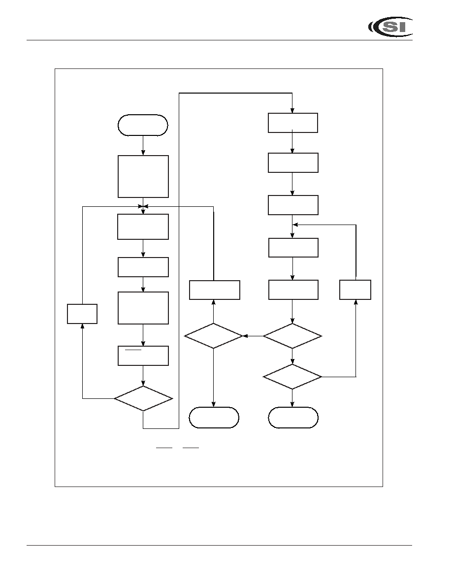
Figure. 6 IC89C52(51)A Main Memory Programming Flow
Start
Programming
PLSCNT=0,
Address=0,
Setup Received
Command Mode
(1)
VPP=Vppl,
Setup '40H'
Command
Setup 'C0H'
Command
VPP=Vppl,
Address=0
P2.6 set low pulse
for 100 ns
P2.6 set low pulse
for 100 ns
Programming
Error
Programming
Completed
Setup Address
,Data
VPP=Vpph
orVppl
(2)
Setup Address
& P2.7 = 0
Read Data
& Set P2.7=1
PROG set low
pulse for 200 us
INC
Address
INC
Address
INC PLSCNT
Last Address ?
PLSCNT=10?
Verify Data?
No
No
No
Yes
Yes
1. Received Command Mode status:
RST=1, PSEN=0, PROG=1, VPP=1, P2.6=1, P2.7=1, P3.6=1, P3.7=1
2. The VPP voltage is decided by Signature Byte address(032H)
Yes
Yes
No
Last Address?

IC89C52(51)A
Integrated C ircuitSolution Inc.
11
MC008-0C 11/27/2001
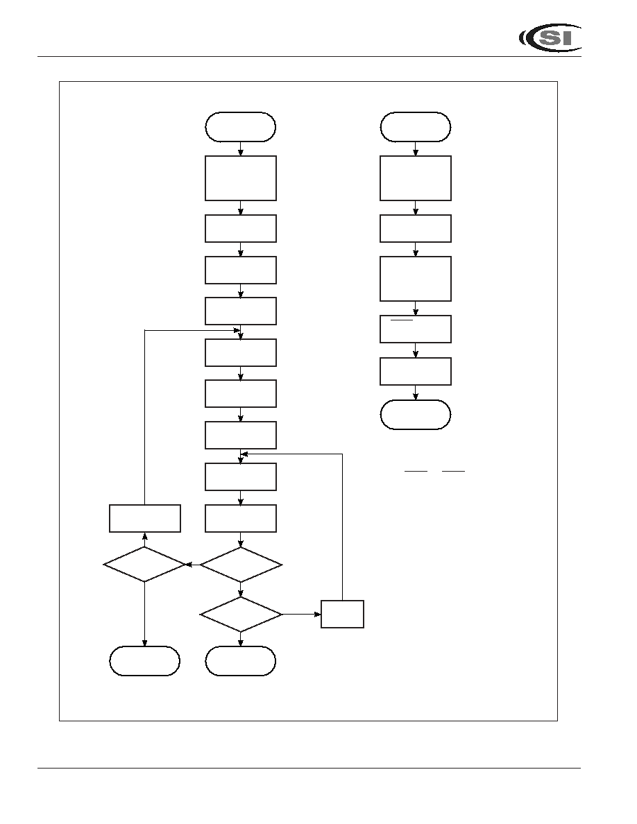
Figure. 7 IC89C52(51)A Lock Bits Programming Flow
Start
Programming
PLSCNT=0,
Setup Received
Command Mode
(1)
Setup '60H'('70H'
,'80H')Command
P2.6 set low pulse
for 100 ns
PROG set low
pulse for 100 ns
Programming
Completed
Setup 'D0H'
Command
VPP=Vpph
or Vppl
(2)
VPP=Vppl
PLSCNT=10?
1. Received Command Mode status:
RST=1, PSEN=0, PROG=1, VPP=1, P2.6=1, P2.7=1, P3.6=1, P3.7=1
2. The VPP voltage is decided by Signature Byte address(032H)
No
Yes
IC89C52(51)A
12
Integrated C ircuitSolution Inc.
MC008-0C 11/27/2001
Figure. 8 IC89C52(51)A Erase Flow
Start
Erase Flow
PLSCNT=0,
Setup Received
Command Mode
(1)
Programming all
data to '00'
(4)
PLSCNT=0,
Address=00H
Setup 'A0H'
Command
P2.6 set low pulse
for 100 ns
Setup Address
& P2.7 = 0
Read Data
& Set P2.7 = 1
INC
PLSCNT
Erase operation
(2)
Erase operation
(2)
* 2 pulse
Erase
Completed
INC
Address
Data='FF' ?
No
No
No
Yes
Yes
Yes
1. Received Command Mode status:
RST=1, PSEN=0, PROG=1, VPP=1,
P2.6=1, P2.7=1, P3.6=1, P3.7=1
2. The erase operation show in "Erase
Operation" Sub-flow
3. To program main memory to '00',
then program lock bits.
The pre-programming address range
are from 0 to 1FFFH either in
IC89C52A or in IC89C51A
4. The VPP voltage is decided by
Signature Byte address(032H)
Start Erase
operation
VPP=Vppl,
Setup '20H'
Command
Setup 'D0H'
Command,
VPP=Vpph or
Vppl
(5)
P2.6 set low pulse
for 100 ns
VPP=Vppl
PROG set low
pulse for 200 ns
Erase
Completed
Chip Erase Sub-flow
Chip Erase Main flow
Last Address ?
PLSCNT=50 ?
Erase
Error

IC89C52(51)A
Integrated C ircuitSolution Inc.
13
MC008-0C 11/27/2001
OPERATING RANGE
(1)
Range
Ambient Temperature
V
CC
Oscillator Frequency
Commercial
0∞C to +70∞C
5V 10%
3.5 to 40 MHz
Note:
1. Operating ranges define those limits between which the functionality of the device is guaranteed.
ABSOLUTE MAXIMUM RATINGS
(1)
Symbol
Parameter
Value
Unit
V
TERM
Terminal Voltage with Respect to GND
(2)
≠2.0 to +7.0
V
T
BIAS
Temperature Under Bias
(3)
0 to +70
∞C
T
STG
Storage Temperature
≠65 to +125
∞C
P
T
Power Dissipation
1.5
W
Note:
1. Stress greater than those listed under ABSOLUTE MAXIMUM RATINGS may cause
permanent damage to the device. This is a stress rating only and functional operation
of the device at these or any other conditions above those indicated in the operational
sections of this specification is not implied. Exposure to absolute maximum rating
conditions for extended periods may affect reliability.
2. Minimum DC input voltage is ≠0.5V. During transitions, inputs may undershoot to ≠2.
0V for periods less than 20 ns. Maximum DC voltage on output pins is Vcc + 0.5V
which may overshoot to Vcc + 2.0V for periods less than 20 ns.
3. Operating temperature is for commercial products only defined by this specification.
Warning:
Stressing the device beyond the "Absolute Maximum Rating" may cause permanent
damage. This is stress rating only. Operation beyond the "operating conditions" is not
recommended and extended exposure beyond the "operating conditions" may affect
device reliability.

IC89C52(51)A
14
Integrated C ircuitSolution Inc.
MC008-0C 11/27/2001
DC CHARACTERISTICS
(Ta=0∞C to 70∞C; VCC=5V+10%; VSS=0V )
Symbol
Parameter
Test conditions
Min
Max
Unit
V
IL
Input low voltage (All except
EA
)
≠0.5
0.2Vcc ≠ 0.1
V
V
IL
1
Input low voltage (
EA
)
≠0.5
0.2Vcc ≠ 0.3
V
V
IH
Input high voltage
0.2Vcc + 0.9
Vcc + 0.5
V
(All except XTAL 1, RST,
EA
)
V
IH
1
Input high voltage (XTAL 1,
EA
)
0.7Vcc
Vcc + 0.5
V
V
SCH
+
RST positive schmitt-trigger
0.7Vcc
Vcc + 0.5
V
threshold voltage
V
SCH
≠
RST negative schmitt-trigger
0
0.3Vcc
V
threshold voltage
V
OL
(1)
Output low voltage
Iol = 100 µA
--
0.3
V
(Ports 1, 2, 3)
I
OL
= 1.6 mA
--
0.45
V
I
OL
= 3.5 mA
--
1.0
V
V
OL
1
(1)
Output low voltage
I
OL
= 200 µA
--
0.3
V
(Port 0, ALE,
PSEN
)
I
OL
= 3.2 mA
--
0.45
V
I
OL
= 7.0 mA
--
1.0
V
V
OH
Output high voltage
I
OH
= ≠10 µA
0.9Vcc
--
V
(Ports 1, 2, 3, ALE,
PSEN
)
Vcc = 4.5V-5.5V
I
OL
= ≠25 µA
0.75Vcc
--
V
I
OL
= ≠60 µA
2.4
--
V
V
OH
1
Output high voltage
I
OH
= ≠80 µA
0.9Vcc
--
V
(Port 0, ALE,
PSEN
)
Vcc = 4.5V-5.5V
I
OH
= ≠300 µA
0.75Vcc
--
V
I
OH
= ≠800 µA
2.4
--
V
I
IL
Logical 0 input current (Ports 1, 2, 3) V
IN
= 0.45V
--
≠50
µA
I
LI
Input leakage current (Port 0)
0.45V < V
IN
< Vcc
≠10
+10
µA
I
TL
Logical 1-to-0 transition current
V
IN
= 2.0V
--
≠650
µA
(Ports 1, 2, 3)
R
RST
RST pulldown resister
V
IN
=0v
50
300
K
Note:
1. Under steady state (non-transient) conditions, I
OL
must be externally limited as follows:
Maximum I
OL
per port pin:
10 mA
Maximum I
OL
per 8-bit port
Port 0: 26 mA
Ports 1, 2, 3: 15 mA
Maximum total I
OL
for all output pins: 71 mA
If I
OL
exceeds the test condition, V
OL
may exceed the related specification.
Pins are not guaranteed to sink greater than the listed test conditions.
2.The Icc test conditions are shown below. Minimum V
CC
for Power Down is 2 V.

IC89C52(51)A
Integrated C ircuitSolution Inc.
15
MC008-0C 11/27/2001
POWER SUPPLY CHARACTERISTICS
Symbol
Parameter
Test conditions
Min
Max
Unit
Icc
Power supply current
(1)
Vcc = 5.0V
Active mode
12 MHz
--
20
mA
16 MHz
--
26
mA
20 MHz
--
32
mA
24 MHz
--
38
mA
32 MHz
--
50
mA
40 MHz
--
62
mA
Idle mode
12 MHz
--
5
mA
16 MHz
--
6
mA
20 MHz
--
7.6
mA
24 MHz
--
9
mA
32 MHz
--
12
mA
40 MHz
--
15
mA
Power-down mode
V
CC
= 5V
--
100
µA
Note:
1. See Figures 9,10,11, and 12 for Icc test conditiions.
Figure 9. Active Mode
Figure 10. Idle Mode
Figure 11. Power-down Mode
(Vcc=2.0V~6.0V)
XTAL1
GND
NC
RST
Vcc
P0
EA
Vcc
Vcc
CLOCK
SIGNAL
Icc
XTAL2
Vcc
XTAL1
GND
NC
RST
Vcc
P0
EA
Vcc
Vcc
CLOCK
SIGNAL
Icc
XTAL2
XTAL1
GND
NC
RST
Vcc
P0
EA
Vcc
Vcc
Icc
XTAL2
IC89C52(51)A
16
Integrated C ircuitSolution Inc.
MC008-0C 11/27/2001
Figure 12. Clock Signal Waveform for I
CC
Tests in Active and Idle Mode (t
CLCH
=t
CHCL
=5 ns)
AC CHARACTERISTICS
(Ta=0∞C to 70 ∞C; V
CC
=5V 10%; V
SS
=0V; C1 for port 0, ALE and
PSEN
Outputs=100pF; C1 for other outputs=80pF)
EXTERNAL MEMORY CHARACTERISTICS
24 MHz
40 MHz
Variable Oscillator
Clock
Clock
(3.5 - 40 MHz)
Symbol
Parameter
Min
Max
Min Max
Min
Max
Unit
1/t
CLCL
Oscillator frequency
--
--
--
--
3.5
40
MHz
t
LHLL
ALE pulse width
68
--
35
--
2t
CLCL
≠15
--
ns
t
AVLL
Address valid to ALE low
26
--
10
--
t
CLCL
≠15
--
ns
t
LLAX
Address hold after ALE low
31
--
15
--
t
CLCL
≠10
--
ns
t
LLIV
ALE low to valid instr in
--
147
--
80
--
4t
CLCL
≠20
ns
t
LLPL
ALE low to
PSEN
low
31
--
15
--
t
CLCL
≠10
--
ns
t
PLPH
PSEN
pulse width
110
--
60
--
3t
CLCL
≠15
--
ns
t
PLIV
PSEN
low to valid instr in
--
105
--
55
--
3t
CLCL
≠20
ns
t
PXIX
Input instr hold after
PSEN
0
--
0
--
0
--
ns
t
PXIZ
Input instr float after
PSEN
--
37
--
20
--
t
CLCL
≠5
ns
t
AVIV
Address to valid instr in
--
188
--
105
--
5t
CLCL
≠20
ns
t
PLAZ
PSEN
low to address float
--
10
--
10
--
10
ns
t
RLRH
RD
pulse width
230
--
130
--
6t
CLCL
≠20
--
ns
t
WLWH
WR
pulse width
230
--
130
--
6t
CLCL
≠20
--
ns
t
RLDV
RD
low to valid data in
--
157
--
90
--
4t
CLCL
≠10
ns
t
RHDX
Data hold after
RD
0
--
0
--
0
--
ns
t
RHDZ
Data float after
RD
--
78
--
45
--
2t
CLCL
≠5
ns
t
LLDV
ALE low to valid data in
--
282
--
165
--
7t
CLCL
≠10
ns
t
AVDV
Address to valid data in
--
323
--
190
--
8t
CLCL
≠10
ns
t
LLWL
ALE low to
RD
or
WR
low
105
145
55
95
3t
CLCL
≠20
3t
CLCL
+20
ns
t
AVWL
Address to
RD
or
WR
low
146
--
80
--
4t
CLCL
≠20
--
ns
t
QVWX
Data valid to
WR
transition
26
--
10
--
t
CLCL
≠15
--
ns
t
WHQX
Data hold after
WR
31
--
15
--
t
CLCL
≠10
--
ns
t
RLAZ
RD
low to address float
--
0
--
0
--
0
ns
t
WHLH
RD
or
WR
high to ALE high
26
57
10
40
t
CLCL
≠15
t
CLCL
+15
ns
0.45V
Vcc -- 0.5V
t
CHCX
t
CLCL
t
CLCH
t
CLCX
t
CHCL
0.7Vcc
0.2Vcc -- 0.1

IC89C52(51)A
Integrated C ircuitSolution Inc.
17
MC008-0C 11/27/2001
SERIAL PORT TIMING: SHIFT REGISTER MODE
24 MHz
40 MHz
Variable Oscillator
Clock
Clock
(3.5-40 MHz)
Symbol
Parameter
Min
Max
Min Max
Min
Max
Unit
t
XLXL
Serial port clock cycle time
490
--
290
--
12t
CLCL
≠10
--
ns
t
QVXH
Output data setup to
327
--
160
--
10t
CLCL
≠90
--
ns
clock rising edge
t
XHQX
Output data hold after
58
--
25
--
2t
CLCL
≠25
--
ns
clock rising edge
t
XHDX
Input data hold after
0
--
0
--
0
--
ns
clock rising edge
t
XHDV
Clock rising edge to
--
284
--
117
--
10t
CLCL
--133
ns
input data valid
EXTERNAL CLOCK DRIVE CHARACTERISTICS
Symbol
Parameter
Min
Max
Unit
1/t
CLCL
Oscillator Frequency
3.5
40
MHz
t
CHCX
High time
10
--
ns
t
CLCX
Low time
10
--
ns
t
CLCH
Rise time
--
10
ns
t
CHCL
Fall time
--
10
ns
Symbol
Parameter
Min
Max
Unit
Vcc
Programming and Erase Power Voltage
5.25
5.75
V
Vpp
Programming and Erase Enable Voltage
11.5
12.5
V
Ipp
Programming and Erase Enable Current
-
2.0
mA
tDVCL
Data Valid to Command Setup Low
10
-
ns
tCLCH
Command Setup Width
100
-
ns
tCHDX
Data Hold after Command Setup
10
-
ns
tAVGL
Address Setup to
PROG
Low
20
-
ns
tGHAX
Address Hold after
PROG
20
-
ns
tDVGL
Data Setup to
PROG
Low
20
-
ns
tGHDX
Data Hold after
PROG
20
-
ns
tSHGL
Vpp Setup to
PROG
Low
10
-
us
tGHSL
Vpp Hold after
PROG
10
-
us
tGLGH
PROG
Pulse Width in Programming Cycle
200
-
us
tGLGHE
PROG
Pulse Width in Erase Cycle
200
-
ms
tAVQV
Address Valid to Data Valid
-
50
ns
tELQV
ENABLE
Low to Data Valid
-
50
ns
tAXQX
Data Float after Address Float
0
-
ns
tEHQX
Data Float after
ENABLE
0
-
ns
Flash Program/Erase and Verification & Test Mode Characteristics

IC89C52(51)A
18
Integrated C ircuitSolution Inc.
MC008-0C 11/27/2001
Figure 14. External Data Memory Read Cycle
TIMING WAVEFORMS
t
LHLL
ALE
t
AVLL
t
LLPL
t
PLPH
t
PLIV
t
LLAX
t
PLAZ
t
PXIZ
t
PXIX
A7-A0
INSTR IN
A7-A0
t
LLIV
t
AVIV
PSEN
PORT 0
PORT 2
A15-A8
A15-A8
t
LLDV
t
AVLL
A7-A0 FROM RI OR DPL
INSTR IN
A7-A0 FROM PCL
t
AVWL
t
AVDV
PSEN
PORT 0
PORT 2
ALE
RD
DATA IN
A15-A8 FROM DPH
A15-A8 FROM PCH
t
WHLH
t
LLWL
t
LLAX
t
RLAZ
t
RLDV
t
RHDZ
t
RHDX
t
RLRH
Figure 13. External Program Memory Read Cycle
IC89C52(51)A
Integrated C ircuitSolution Inc.
19
MC008-0C 11/27/2001
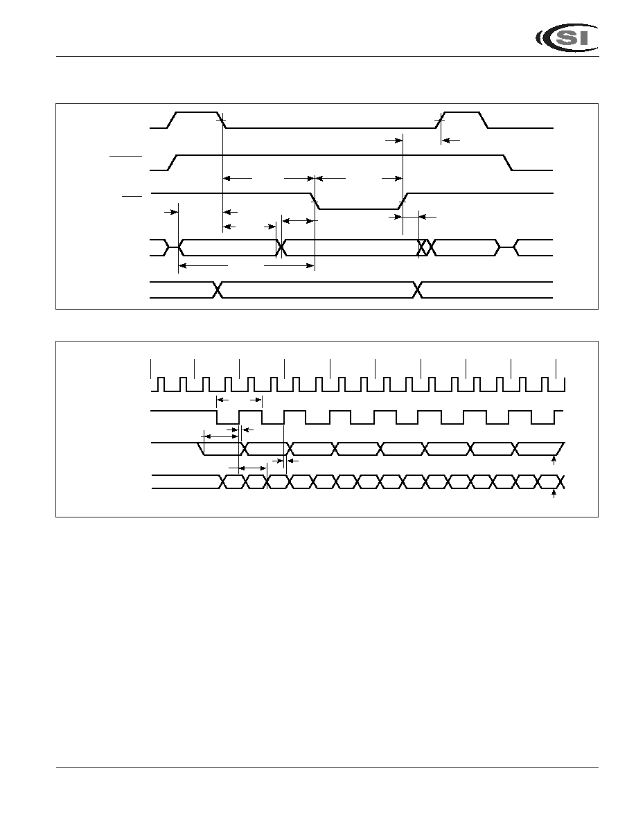
Figure 15. External Data Memory Write Cycle
Figure 16. Shift Register Mode Timing Waveform
t
AVLL
A7-A0 FROM RI OR DPL
INSTR IN
A7-A0 FROM PCL
t
AVWL
PSEN
PORT 0
PORT 2
ALE
WR
DATA OUT
A15-A8 FROM DPH
A15-A8 FROM PCH
t
WHLH
t
LLWL
t
LLAX
t
QVWX
t
WHQX
t
WLWH
INSTRUCTION
ALE
CLOCK
DATA
OUT
DATA
IN
t
XLXL
t
XHQX
t
QVXH
t
XHDV
t
XHDX
VALID
VALID
VALID
VALID
VALID
VALID
VALID
VALID
SET TI
SET RI
7
8
6
5
4
3
2
1
0
7
6
5
4
3
2
1
0
IC89C52(51)A
20
Integrated C ircuitSolution Inc.
MC008-0C 11/27/2001
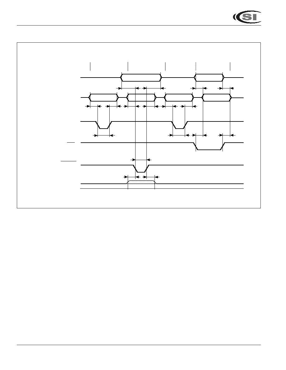
Figure 17. Programming Timing Wavform
P2.4-P2.0
P1.7-P1.0
PROG
VPP
t
AVGL
t
DVCL
t
CLCH
t
CLCH
t
ELQV
t
EHQX
t
GLGH
t
GHSL
t
SHGL
t
CHDX
t
DVGL
t
GHDX
t
DVCL
t
CHDX
t
GHAX
t
AVQV
t
AXQX
ADDRESS IN
ADDRESS IN
PROGRAM
SETUP CYCLE
PROGRAM
CYCLE
PROGRAM VERIFY
SETUP CYCLE
PROGRAM
VERIFY CYCLE
DATA OUT
P0
P2.6
(Command Setup)
P2.7(OE)
DATA IN
40H
C0H

IC89C52(51)A
Integrated C ircuitSolution Inc.
21
MC008-0C 11/27/2001
Figure 18. Erase Timing Waveform
Figure 19. External Clock Drive Waveform
Figure 20. AC Test Point
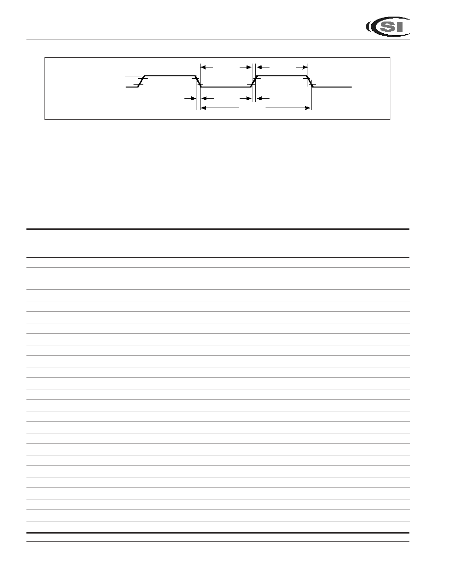
Note:
1.AC inputs during testing are driven at Vcc-0.5v for logic "1" and 0.45V for logic "0".
Timing measurements are made at Vih min for logic "1" and max for logic "0".
0.45V
Vcc -- 0.5V
t
CHCX
t
CLCL
t
CLCH
t
CLCX
t
CHCL
0.7Vcc
0.2Vcc -- 0.1
Vcc - 0.5V
0.45V
0.2Vcc + 0.9V
0.2Vcc - 0.1V
P2.4-P2.0
P1.7-P1.0
PROG
VPP
t
DVCL
t
CLCH
t
CLCH
t
ELQV
t
EHQX
t
GLGHE
t
GHSL
t
SHGL
t
CHDX
t
DVGL
t
GHDX
t
DVCL
t
CHDX
t
AVQV
t
AXQX
ADDRESS IN
ERASE
SETUP CYCLE
ERASE CYCLE
ERASE VERIFY
SETUP CYCLE
ERASE
VERIFY CYCLE
DATA OUT
P0
P2.6
(Command Setup)
P2.7(OE)
D0H
20H
A0H

IC89C52(51)A
22
Integrated C ircuitSolution Inc.
MC008-0C 11/27/2001
ORDERING INFORMATION
Commercial Range: 0∞C to +70∞C
Speed
Order Part Number
Package
12 MHz
IC89C52(51)A-12PL
PLCC
IC89C52(51)A-12W
600mil DIP
IC89C52(51)A-12PQ
PQFP
24 MHz
IC89C52(51)A-24PL
PLCC
IC89C52(51)A-24W
600mil DIP
IC89C52(51)A-24PQ
PQFP
40 MHz
IC89C52(51)A-40PL
PLCC
IC89C52(51)A-40W
600mil DIP
IC89C52(51)A-40PQ
PQFP
Integrated C ircuitSolution Inc.
HEADQUARTER:
NO.2, TECHNOLOGY RD. V, SCIENCE-BASED INDUSTRIAL PARK,
HSIN-CHU, TAIWAN, R.O.C.
TEL: 886-3-5780333
Fax: 886-3-5783000
BRANCH OFFICE:
7F, NO. 106, SEC. 1, HSIN-TAI 5
TH
ROAD,
HSICHIH TAIPEI COUNTY, TAIWAN, R.O.C.
TEL: 886-2-26962140
FAX: 886-2-26962252
http://www.icsi.com.tw