IC89C54/58/64
Integrated Circuit Solution Inc.
1
MC009-0B
ICSI reserves the right to make changes to its products at any time without notice in order to improve design and supply the best possible product. We assume no responsibility for any errors
which may appear in this publication. © Copyright 2000, Integrated Circuit Solution Inc.
IC89C54/58/64
CMOS SINGLE CHIP
8-BIT MICROCONTROLLER
with 16/32/64-Kbytes of FLASH
FEATURES
∑ 80C52 based architecture
∑ 16K/32K/64K Byte Flash Memory with fast-
pulse programming algorithm
∑ 256 x 8 RAM
∑ Three 16-bit Timer/Counters
∑ Full duplex serial channel
∑ Boolean processor
∑ Four 8-bit I/O ports, 32 I/O lines
∑ Memory addressing capability
≠ 64K Program Memory and 64K Data Memory
∑ Program memory lock
≠ Lock bits (3)
∑ Power save modes:
≠ Idle and power-down
∑ Eight interrupt sources
∑ Most instructions execute in 0.3 µs
∑ CMOS and TTL compatible
∑ Maximum speed: 40 MHz @ Vcc = 5V
∑ Packages available:
≠ 40-pin DIP
≠ 44-pin PLCC
≠ 44-pin PQFP
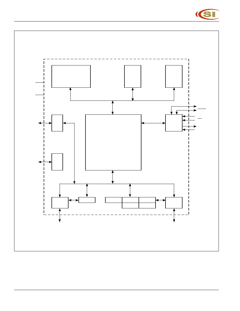
GENERAL DESCRIPTION
IC89C54, IC89C58, IC89C64 are members of
ICSI
embedded microcontroller family. The IC89C54/58/64 uses
the same powerful instruction set, has the same architecture,
and is pin-to-pin compatible with standard 80C52 controller
devices. IC89C54/58/64 are just changed internal Flash
size, other features are same as standard IC89C52.
The IC89C54/58/64 contains a 16K/32K/64K x 8 Flash;
a 256 x 8 RAM; 32 I/O lines for either multi-processor
communications; I/O expansion or full duplex UART; three
16-bit timers/counters; an eight-source, two-priority-level,
nested interrupt structure; and on chip oscillator and clock
circuit. The IC89C54/58/64 can be expanded using standard
TTL compatible memory.
Figure 1. IC89C54/58/64 Pin Configuration: 40-pin DIP
1
2
3
4
5
6
7
8
9
10
11
12
13
14
15
16
17
18
19
20
40
39
38
37
36
35
34
33
32
31
30
29
28
27
26
25
24
23
22
21
T2/P1.0
T2EX/P1.1
P1.2
P1.3
P1.4
P1.5
P1.6
P1.7
RST
RxD/P3.0
TxD/P3.1
INT0/P3.2
INT1/P3.3
T0/P3.4
T1/P3.5
WR/P3.6
RD/P3.7
XTAL2
XTAL1
GND
VCC
P0.0/AD0
P0.1/AD1
P0.2/AD2
P0.3/AD3
P0.4/AD4
P0.5/AD5
P0.6/AD6
P0.7/AD7
EA/VPP
ALE/PROG
PSEN
P2.7/A15
P2.6/A14
P2.5/A13
P2.4/A12
P2.3/A11
P2.2/A10
P2.1/A9
P2.0/A8

IC89C54/58/64
Integrated Circuit Solution Inc.
5
MC009-0B
Table 1. Detailed Pin Description
Symbol
PDIP
PLCC
PQFP
I/O
Name and Function
ALE/
PROG
30
33
27
I/O
Address Latch Enable: Output pulse for latching the low byte
of the address during an address to the external memory. In
normal operation, ALE is emitted at a constant rate of 1/6 the
oscillator frequency, and can be used for external timing or
clocking. Note that one ALE pulse is skipped during each
access to external data memory. This pin is also the Program
Pulse input (
PROG) during Flash programming.
EA/V
PP
31
35
29
I
External access enable: EA# must be externally held low to enable
the device to fetch code from external program memory locations
0000H to FFFFH. If EA# is held high, the device executes from internal
program memory unless the program counter contains an address
grater than 3FFFH/7FFFH respecting to IC89C54/58 and the device
always executes internal program memory in IC89C64.
This is also receives the 12 V programming enable voltage (Vpp)
during Flash programming, when 12 V programming is selected.
P0.0-P0.7
39-32
43-36
37-30
I/O
Port 0: Port 0 is an open-drain, bi-directional I/O port. Port 0 pins
that have 1s written to them float and can be used as high-
impedance inputs. Port 0 is also the multiplexed low-order
address and data bus during accesses to external program and
data memory. In this application, it uses strong internal pullups
when emitting 1s.
Port 0 also receives the command and code bytes during
memory program and verification, and outputs the code bytes
during program verification. External pullups are required dur-
ing program verification.
P1.0-P1.7
1-8
2-9
40-44
I/O
Port 1: Port 1 is an 8-bit bi-directional I/O port with internal pull-
ups. Port 1 pins that have 1s written to them are pulled high by
the internal pullups and can be used as inputs. As inputs, port
1 pins that are externally pulled low will source current because
of the internal pullups.
Port 1 also receives the low-order address byte during memory
program and verification.
1
2
40
I
T2(P1.0) : Timer/counter 2 external count input.
2
3
41
I
T2EX(P1.1): Timer/counter 2 trigger input.
P2.0-P2.7
21-28
24-31
18-25
I/O
Port 2: Port 2 is an 8-bit bi-directional I/O port with internal pull-
ups. Port 2 pins that have 1s written to them are pulled high by
the internal pullups and can be used as inputs. As inputs, port
2 pins that are externally pulled low will source current because
of the internal pullups. Port 2 emits the high order address byte
during fetches from external program memory and during
accesses to external data memory that used 16-bit addresses.
In this application, it uses strong internal pullups when emitting
1s. During accesses to external data memory that use 8-bit
addresses, port 2 emits the contents of the P2 special function
register.
Port 2 also receives the high-order address bits from A13 to A8
and some control signals during Flash programming and
verification. P2.6, P2.7 are the control signals while the chip
programs and erases. P2.6 is a program command strobe
signal. P2.7 is a data output enable signal.