IC89E54/58/64
Integrated C ircuitSolution Inc.
1
MC012-0C 11/16/2001
ICSI reserves the right to make changes to its products at any time without notice in order to improve design and supply the best possible product. We assume no responsibility for any errors
which may appear in this publication. © Copyright 2000, Integrated Circuit Solution Inc.
8-BITS SINGLE MICROCONTROLLER
with 16/32/64-Kbytes of FLASH,
256 byte +512 byte RAM
FEATURES
∑ 80C52 based architecture
∑ 256 Byte RAM internal RAM and 512 Bytes
auxiliary RAM available
∑ Three 16-bit Timer/Counters
∑ Full duplex serial channel
∑ Boolean processor
∑ Power Save Mode :
1) Idle Mode
2) Power Down Mode - waken up from interrupt
level trigger mode
∑ Program memory lock
≠ Lock bits (3)
∑ Four 8-bit I/O ports, 32 I/O lines
∑ Memory addressing capability
≠ 64K Program Memory and 64K Data Memory
∑ CMOS and TTL compatible
∑ Maximum speed ranges at Vcc = 5V is 40 MHz
and most instructions execute in 0.3 µs
∑ Packages available:
≠ 40-pin DIP
≠ 44-pin PLCC
≠ 44-pin PQFP
∑ 16K/32K/64K Byte Flash Memory with fast-pulse
programming algorithm
∑
36 I/O pins(above 44-pin package only)
∑
8 interrupts vectors (above 44-pin package
only)
∑
Low EMI mode
GENERAL DESCRIPTION
IC89E54, IC89E58, IC89E64 are members of ICSI
embedded microcontroller family. The IC89E54/58/64 uses
the same powerful instruction set, has the same architecture,
and is pin-to-pin compatible with standard 80C51 controller
devices. They have IC89E54/58/64 all functions and some
enhanced function is included. These enhanced functions
include 512 bytes auxiliary memory, 36 I/O pins (44 pin
package only), 8 interrupts (44 pin package only) with two-
level priority, Power off flag, Low EMI mode, power down
mode is waken up from interrupt level trigger mode.
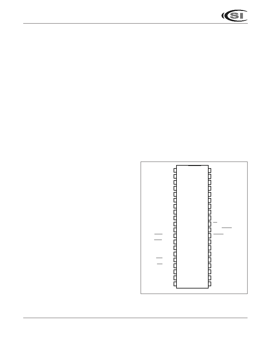
Figure 1. IC89E54/58/64 Pin Configuration: 40-pin DIP
1
2
3
4
5
6
7
8
9
10
11
12
13
14
15
16
17
18
19
20
40
39
38
37
36
35
34
33
32
31
30
29
28
27
26
25
24
23
22
21
T2/P1.0
T2EX/P1.1
P1.2
P1.3
P1.4
P1.5
P1.6
P1.7
RST
RxD/P3.0
TxD/P3.1
INT0/P3.2
INT1/P3.3
T0/P3.4
T1/P3.5
WR/P3.6
RD/P3.7
XTAL2
XTAL1
VSS
VCC
P0.0/AD0
P0.1/AD1
P0.2/AD2
P0.3/AD3
P0.4/AD4
P0.5/AD5
P0.6/AD6
P0.7/AD7
EA/VPP
ALE/PROG
PSEN
P2.7/A15
P2.6/A14
P2.5/A13
P2.4/A12
P2.3/A11
P2.2/A10
P2.1/A9
P2.0/A8

IC89E54/58/64
2
Integrated C ircuitSolution Inc.
MC012-0C 11/16/2001
TOP VIEW
Figure 2. IC89E54/58/64 Pin Configuration: 44-pin PLCC
WR/P3.6
RD/P3.7
XTAL2
XTAL1
VSS
P4.0
A8/P2.0
A9/P2.1
A10/P2.2
A11/P2.3
A12/P2.4
P1.4
P1.3
P1.2
P1.1/T2EX
P1.0/T2
INT3/P4.2
VCC
P0.0/AD0
P0.1/AD1
P0.2/AD2
P0.3/AD3
P0.4/AD4
P0.5/AD5
P0.6/AD6
P0.7/AD7
EA/VPP
P4.1
ALE/PROG
PSEN
P2.7/A15
P2.6/A14
P2.5/A13
P1.5
P1.6
P1.7
RST
RxD/P3.0
INT2/P4.3
TxD/P3.1
INT0/P3.2
INT1/P3.3
T0/P3.4
T1/P3.5
7
8
9
10
11
12
13
14
15
16
17
39
38
37
36
35
34
33
32
31
30
29
INDEX
4
3
6
5
2
1
44
18
19
20
21
22
23
24
43
42
41
40
25
26
27
28

IC89E54/58/64
Integrated C ircuitSolution Inc.
3
MC012-0C 11/16/2001
Figure 3. IC89E54/58/64 Pin Configuration: 44-pin PQFP/LQFP
WR/P3.6
RD/P3.7
XTAL2
XTAL1
VSS
P4.0
A8/P2.0
A9/P2.1
A10/P2.2
A11/P2.3
A12/P2.4
P1.4
P1.3
P1.2
P1.1/T2EX
P1.0/T2
INT3/P4.2
V
CC
P0.0/AD0
P0.1/AD1
P0.2/AD2
P0.3/AD3
P0.4/AD4
P0.5/AD5
P0.6/AD6
P0.7/AD7
EA/VPP
P4.1
ALE/PROG
PSEN
P2.7/A15
P2.6/A14
P2.5/A13
P1.5
P1.6
P1.7
RST
RxD/P3.0
INT2/P4.3
TxD/P3.1
INT0/P3.2
INT1/P3.3
T0/P3.4
T1/P3.5
1
2
3
4
5
6
7
8
9
10
11
33
32
31
30
29
28
27
26
25
24
23
38
12
13
14
15
16
17
18
37
36
35
34
44
43
42
41
40
39
19
20
21
22
IC89E54/58/64
4
Integrated C ircuitSolution Inc.
MC012-0C 11/16/2001
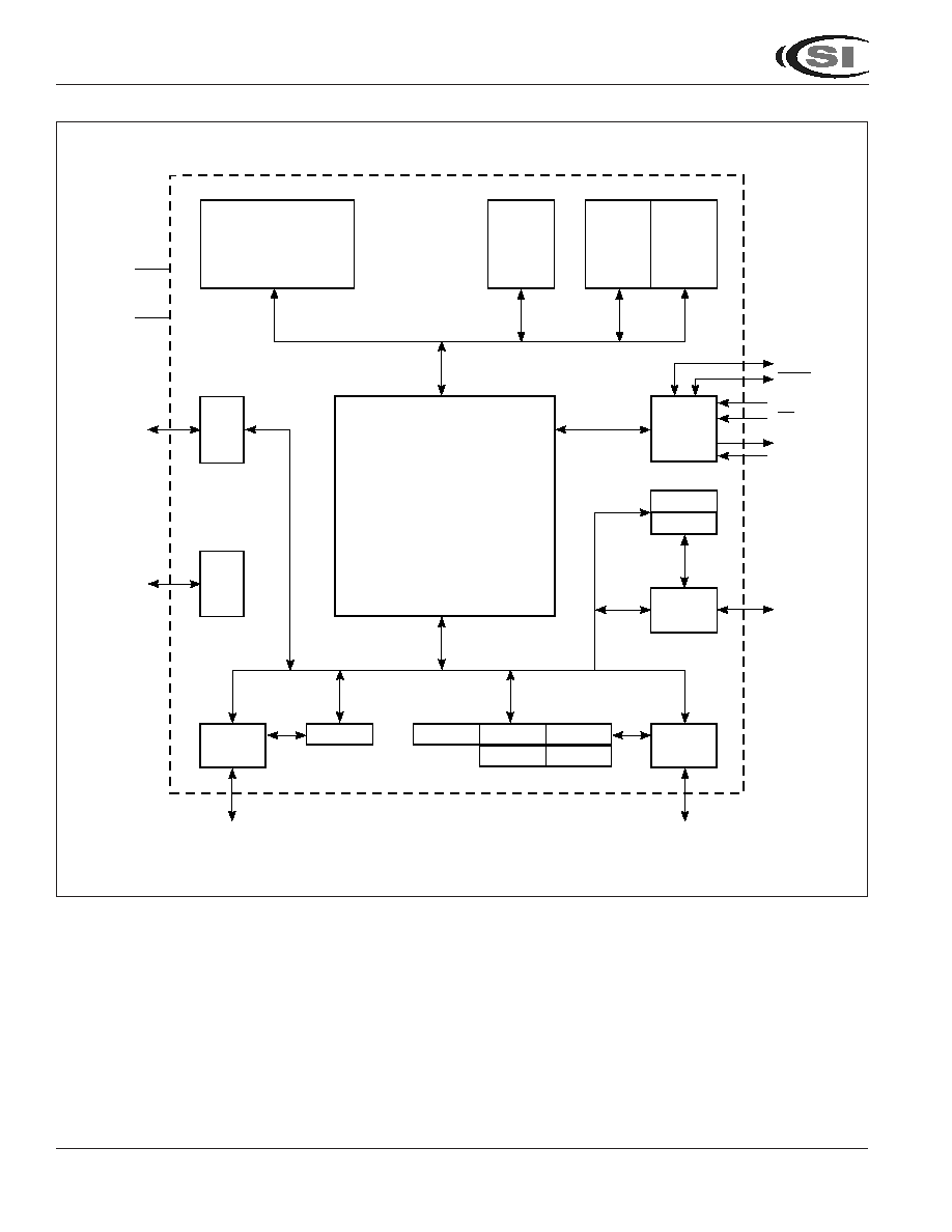
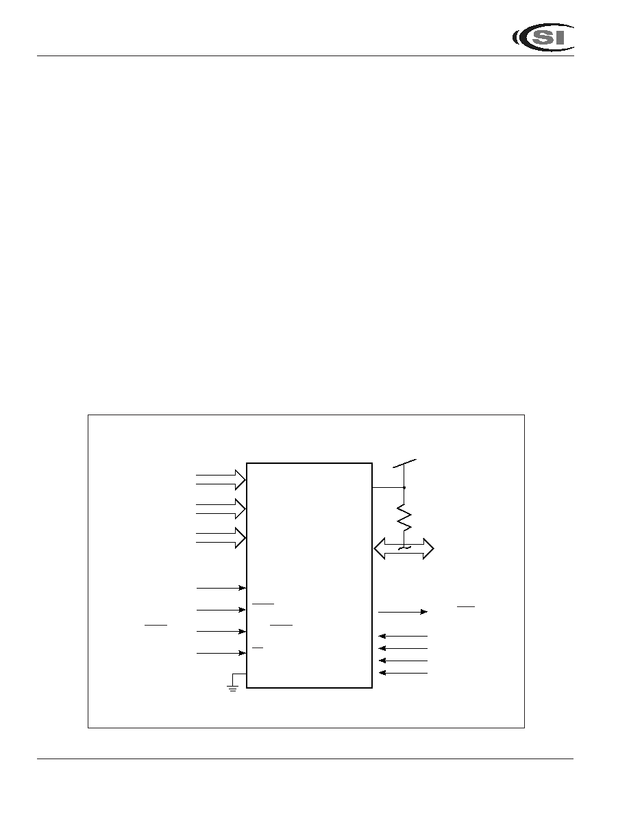
Figure 4. IC89E54/58/64 Block Diagram
PORT 1
PORT 0
PORT 2
PORT 3
P1[7:0]
P0[7:0]
P2[7:0]
P3[7:0]
TIMER 2
UART
INT0
INT1
TIMER 1
TIMER 0
ALE
PSEN
RST
EA
XTAL2
XTAL1
P4[3:0]
16K/32K/64K
MAIN CODE
FLASH
512
BYTE
AUX
RAM
CLOCK
&
TIMING
SFR
BLOCK
VSS
VCC
80C32 CPU CORE
PORT 4
INT 2
INT 3
256
BYTE
RAM

IC89E54/58/64
Integrated C ircuitSolution Inc.
5
MC012-0C 11/16/2001
Table 1. Detailed Pin Description
Symbol
PDIP
PLCC
PQFP
I/O
Name and Function
P0.0-P0.7
39-32
43-36
37-30
I/O
Port 0:
Port 0 is an open-drain, bi-directional I/O port. Port 0 pins
that have 1s written to them float and can be used as high-
impedance inputs. Port 0 is also the multiplexed low-order
address and data bus during accesses to external program and
data memory. In this application, it uses strong internal pullups
when emitting 1s.
Port 0 also receives the command and code bytes during
memory program and verification, and outputs the code bytes
during program verification. External pullups are required during
program verification.
P1.0-P1.7
1-8
2-9
40-44
I/O
Port 1:
Port 1 is an 8-bit bi-directional I/O port with internal
pullups. Port 1 pins that have 1s written to them are pulled high
by the internal pullups and can be used as inputs. As inputs, port
1 pins that are externally pulled low will source current because
of the internal pullups.
Port 1 also receives the low-order address byte during memory
program and verification.
1
2
40
I
T2(P1.0) :
Timer/counter 2 external count input.
2
3
41
I
T2EX(P1.1):
Timer/counter 2 trigger input.
P2.0-P2.7
21-28
24-31
18-25
I/O
Port 2:
Port 2 is an 8-bit bi-directional I/O port with internal
pullups. Port 2 pins that have 1s written to them are pulled high
by the internal pull-ups and can be used as inputs. As inputs,
port 2 pins that are externally pulled low will source current
because of the internal pullups. Port 2 emits the high order
address byte during fetches from external program memory and
during accesses to external data memory that used 16-bit
addresses. In this application, it uses strong internal pullups
when emitting 1s. During accesses to external data memory that
use 8-bit addresses, port 2 emits the contents of the P2 special
function register.
Port 2 also receives the high-order address bits from A13 to A8
and some control signals during Flash programming and
verification. P2.6, P2.7 are the control signals while the chip
programs and erases. P2.6 is a program command strobe
signal. P2.7 is a data output enable signal.

IC89E54/58/64
6
Integrated C ircuitSolution Inc.
MC012-0C 11/16/2001
Table 1. Detailed Pin Description (continued)
Symbol
PDIP
PLCC
PQFP
I/O
Name and Function
P3.0-P3.7
10-17
11, 13-19
5, 7-13
I/O
Port 3:
Port 3 is an 8-bit bi-directional I/O port with internal
pullups. Port 3 pins that have 1s written to them are pulled high
by the internal pullups and can be used as inputs. As inputs, port
3 pins that are externally pulled low will source current because
of the internal pullups.
Port 3 also serves the special features of the IC89E54/58/64, as
listed below:
10
11
5
I
RxD (P3.0):
Serial input port.
11
13
7
O
TxD (P3.1):
Serial output port.
12
14
8
I
INT0
INT0
INT0
INT0
INT0 (P3.2):
External interrupt. Serve as A14 during memory
program and verification.
13
15
9
I
INT1
INT1
INT1
INT1
INT1 (P3.3):
External interrupt. Serve as A15 during memory
program and verification.
14
16
10
I
T0 (P3.4):
Timer 0 external input.
15
17
11
I
T1 (P3.5):
Timer 1 external input.
16
18
12
O
WR
WR
WR
WR
WR (P3.6):
External data memory write strobe. Control signal
during memory program, verification and erase.
17
19
13
O
RD
RD
RD
RD
RD (P3.7):
External data memory read strobe. Control signal
during memory program, verification and erase.
P4.0-P4.3
23
17
I/O
Port 4:
In mode 0, Port 4 is an 8-bit bi-directional I/O port
34
29
with internal pullups. Port 4 pins that have 1s written to them are
1
39
pulled high by the internal pullups and can be used as inputs.
12
6
As inputs, port 4 pins that are externally pulled low will source
current because of the internal pullups.
In mode 1, 2, 3, Port 4 is an address strobe signal which appears
with
RD
or
WR
signals.
12
6
Port 4 also serves the special features, as listed below:
1
39
INT2
INT2
INT2
INT2
INT2 (P4.3):
External interrupt
INT3
INT3
INT3
INT3
INT3 (P4.2):
External interrupt
RST
9
10
4
I
Reset:
A high on this pin for two machine cycles while the
oscillator is running resets the device. An internal resistor to
VSS permits a power-on reset using only an external capacitor.
A small internal resistor permits power-on reset using only a
capacitor connected to VCC.
RST is an input control signal during memory program and
verification.
XTAL 2
18
20
14
O
Crystal 2:
Output from the inverting oscillator amplifier.
XTAL 1
19
21
15
I
Crystal 1:
Input to the inverting oscillator amplifier and input
to the internal clock generator circuits.

IC89E54/58/64
Integrated C ircuitSolution Inc.
7
MC012-0C 11/16/2001
Symbol
PDIP
PLCC
PQFP
I/O
Name and Function
PSEN
29
32
26
O
Program Store Enable:
The read strobe to external program
memory. When the device is executing code from the external
program memory,
PSEN
is activated twice each machine cycle
except that two
PSEN
activations are skipped during each
access to external data memory.
PSEN
is not activated during
fetches from internal program memory.
PSEN
is an input control signal while memory program and
verification.
ALE/
PROG
30
33
27
I/O
Address Latch Enable:
Output pulse for latching the low byte
of the address during an address to the external memory. In
normal operation, ALE is emitted at a constant rate of 1/6 the
oscillator frequency, and can be used for external timing or
clocking. Note that one ALE pulse is skipped during each
access to external data memory.
This pin is also the program pulse input (
PROG
) during pro-
grammable memory programming and erase.
EA
/V
PP
31
35
29
I
External access enable:
EA
must be externally held low to
enable the device to fetch code from external program memory
locations 0000H to FFFFH. If
EA
is held high, the device
executes from internal program memory unless the program
counter contains an address grater than 3FFFH/7FFFH re-
specting to IC89C54/58 and the device always executes inter-
nal program memory in IC89C64.
This is also receives the 12 V programming enable voltage
(Vpp) during Flash programming, when 12 V programming is
selected.
Vss
20
22
16
Ground:
0V reference.
Vcc
40
44
38
I
Power Supply:
This is the power supply voltage for operation.
Table 1. Detailed Pin Description (continued)
OPERATING DESCRIPTION
The detail description of the IC89E54/58/64 included in this
description are:
∑ Memory Map and Registers
∑ Timer/Counters
∑ Serial Interface
∑ Interrupt System
∑ Other Information
∑ Flash Memory
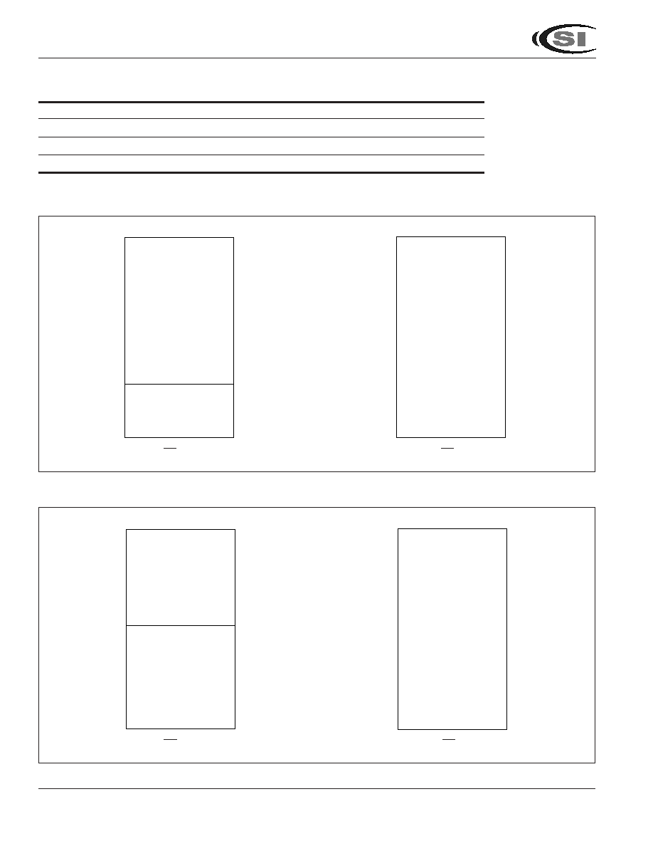
MEMORY MAP AND REGISTERS
Program Memory and data memory
Table 2 shows program memory and data memory size
versus three products. The IC89E54/58/64 series includes
a standard IC80C32 and a 16K/32K/64K Flash Memory. The
IC89E54/58/64 includes IC80C32, a 16K/32K/64K Flash
and some enhanced functions. The figures 3~5 show
IC89E54/58/64 program memory architecture and program
memory access status versus
EA
pin. These enhanced
functions are described in later descriptions. The program
memory and data memory access ranges are listed table 1.
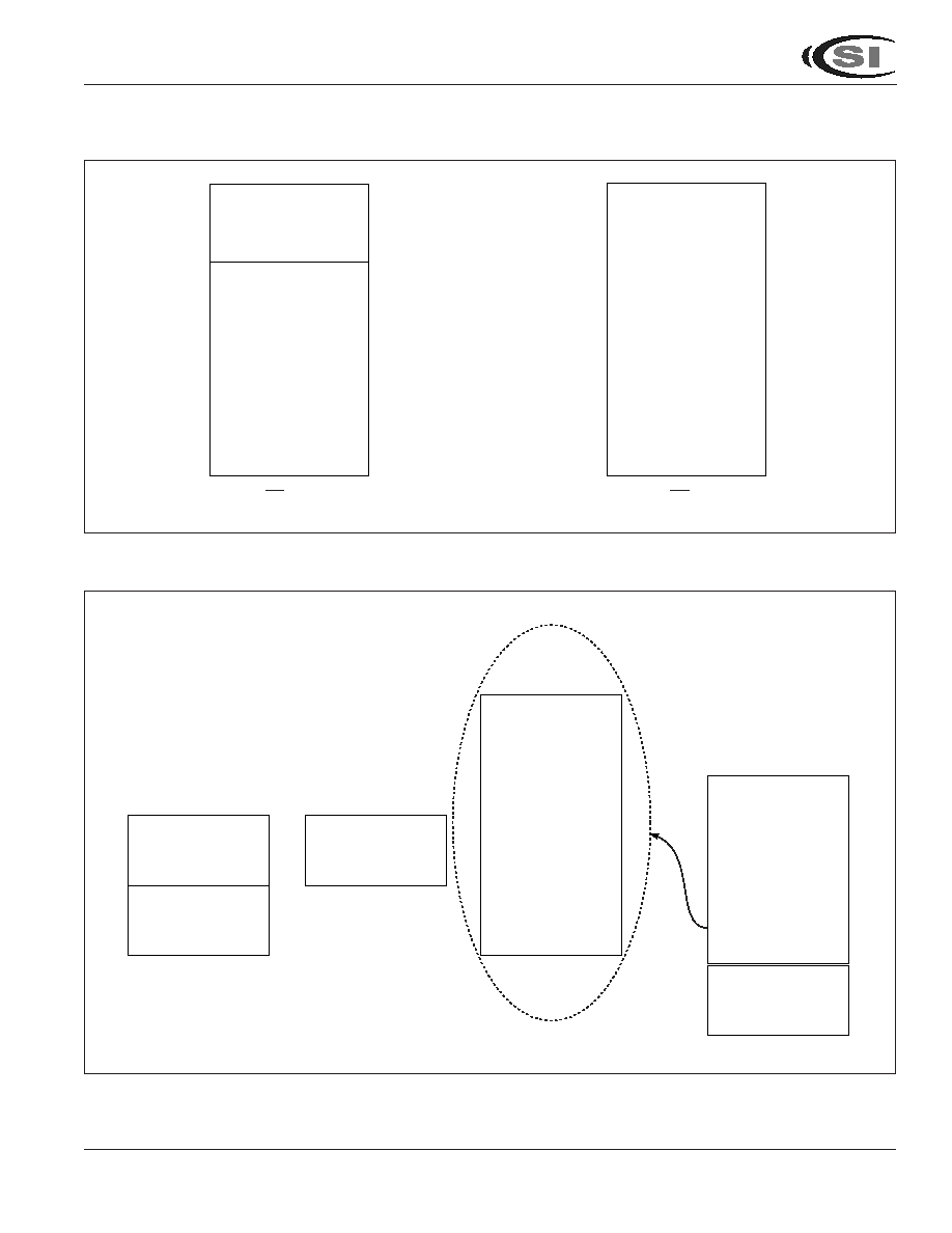
The AUX RAM status is disable after reset, so MOVX
instructions will access external RAM. If set ENARAM bit,
the AUX RAM will be enabled and MOVX instructions will
access AUX RAM in 0000H~01FFH, access external RAM
in 0200H~FFFFH. Figure 6 shows the external data memory
and AUX RAM accesses relation.
IC89E54/58/64
8
Integrated C ircuitSolution Inc.
MC012-0C 11/16/2001
Figure 5. IC89E54 Flash Architecture
Figure 6. IC89E58 Flash Architecture
Table 2. Program memory and Data memory sizes
Main Flash
RAM Size
AUX RAM Size
IC89E54
16K Bytes : [0H~3FFFH]
256 Bytes : [ 0-FFH]
512 Bytes : [ 0-1FFH]
IC89E58
32K Bytes : [0H~7FFFH]
256 Bytes : [ 0-FFH]
512 Bytes : [ 0-1FFH]
IC89E64
64K Bytes : [0H~FFFFH]
256 Bytes : [ 0-FFH]
512 Bytes : [ 0-1FFH]
Internal Range
EA = 1
4000H
3FFFH
0000H
FFFFH
0000H
FFFFH
External Range
External Range
EA = 0
Internal Range
EA = 1
8000H
7FFFH
0000H
FFFFH
0000H
FFFFH
External Range
External Range
EA = 0
IC89E54/58/64
Integrated C ircuitSolution Inc.
9
MC012-0C 11/16/2001
Figure 7. IC89E64 Flash Architecture
Figure 8. IC89E54/58/64 Data Memory Architecture
Internal Range
(Block 1)
EA = 1
F000H
EFFFH
0000H
FFFFH
0000H
FFFFH
Internal Range
(Block 2)
External Range
EA = 0
Direct/Indirect RAM
7FH
00H
Indirect RAM
FFH
80H
SFR
FFH
80H
0000H
FFFFH
External Range
EXTRAM = 0
Auxiliary
Internal RAM
01FFH
0000H
External RAM
FFFFH
0200H
EXTRAM = 1

IC89E54/58/64
10
Integrated C ircuitSolution Inc.
MC012-0C 11/16/2001
Figure 9. IC89E54/58/64 SFRs Map and Reset value (The gray blocks are non-standard.)
B
00000000
ACC
00000000
P4[3:0]
XXXX1111
PSW
00000000
T2CON
00000000
XICON
00000000
IP
XX000000
IE
0X000000
SCON
00000000
TCON
00000000
P0
11111111
P1
11111111
P2
11111111
P3
11111111
SBUF
XXXXXXXX
TMOD
00000000
SP
00000000
DPL
00000000
TL0
00000000
P4CONA
00000000
RCAP2L
00000000
RCAP2H
00000000
P4CCONB
00000000
TL1
00000000
DPH
00000000
TL2
00000000
P43AL
00000000
P42AL
00000000
P41AL
00000000
TH0
00000000
P40AL
00000000
TH2
00000000
PH43AH
00000000
P42AH
00000000
P41AH
00000000
TH1
00000000
P40AH
00000000
P2ECON
0000XX00
P2EAL
00000000
AUXR
XXX00000
P2EAH
00000000
PCON
0XX00000
F8H
F0H
E8H
E0H
D8H
D0H
C8H
C0H
B8H
B0H
A8H
A0H
98H
90H
88H
80H
FFH
F7H
EFH
E7H
DFH
D7H
CFH
C7H
BFH
B7H
AFH
A7H
9FH
97H
8FH
87H
These descriptions are added from standard IC80C32. So, more information for SFRs and memory refer to IC80C32.
IC89E54/58/64
Integrated C ircuitSolution Inc.
11
MC012-0C 11/16/2001
The timers/counters
Refer to IC80C32 data sheet.
The serial interface
Refer to IC80C32 data sheet.
The interrupt system
There are 8 interrupt vectors in 44 pins package and 6 interrupt vectors in 40 pins package. Eight interrupt vectors only
exist in IC89E54/58/64 series.
INT2
and
INT3
are new interrupts that add on standard IC80C32. The interrupt information
shows in Table 3. The interrupt architecture shows in figure 10. External interrupt 2 and 3 control register is XICON shown
in following.
Two additional external interrupts,
INT2
and
INT3
, whose function are similar to those of external interrupt 0 and 1 in
the standard 80C32. The functions/status of these interrupts are determined/shown by the bits in the XICON(External
Interrupt Control) register. The XICON register is bit-addressable but is not a standard register in the 80C32. Its address
is at 0C0H. To set/clear bits in the XICON register, one can use the "SETB (/CLR) bit" instruction.
Table 3. Eight interrupt information
Interrupt Source
Vector Address
Polling Sequence
Enable Required
Interrupt Type
within priority leve
Settings
Edge/Level
External Interrupt 0
03H
0 (Highest)
IE.0
TCON.0
Timer/Counter 0
0BH
1
IE.1
-
External Interrupt 1
13H
2
IE.2
TCON.2
Timer/Counter 1
1BH
3
IE.3
-
Serial Port
23H
4
IE.4
-
Timer/Counter 2
2BH
5
IE.5
-
External Interrupt 2
(1)
33H
6
XICON.2
XICON.0
External Interrupt 3
(1)
3BH
7 (Lowest)
XICON.6
XICON.3
Note:
1. Interrupt 2 and interrupt 3 exist in IC89E54/58/64 44 pins package.

IC89E54/58/64
12
Integrated C ircuitSolution Inc.
MC012-0C 11/16/2001
XICON(C0H)
B7
B6
B5
B4
B3
B2
B1
B0
Flag Name
PX3
EX3
IE3
IT3
PX2
EX2
IE2
IT2
Bit
Name
Description
7
PX3
External interrupt 3 priority high if set.
6
EX3
External interrupt 3 enable if set.
5
IE3
If IT3=1, IE3 is set/cleared automatically by hardware when interrupt is detected/serviced.
4
IT3
External interrupt 3 is falling-edge/low-level triggered when this bit is set/cleared by software.
3
PX2
External interrupt 2 priority high if set.
2
EX2
External interrupt 2 enable if set.
1
IE2
If IT2=1, IE2 is set/cleared automatically by hardware when interrupt is detected/serviced.
0
IT2
External interrupt 2 is falling-edge/low-level triggered when this bit is set/cleared by software.
Figure 10. IC89E54/58/64 Interrupt Architecture
INT0
TF0
TF1
RI/TI
TF2/EXF2
INT2
INT3
IE0
XICON.6
XICON.2
XICON.3
XICON.0
IT0
EA
EX0
ET0
EX1
ET1
ES
ET2
EX2
EX3
IT3
IT2
PT2
PS
PT1
PX1
PT0
PX0
INT1
IE1
IT1
These descriptions are added from standard 80C32. So, more detailed information for interrupts refer to IC80C52.

IC89E54/58/64
Integrated C ircuitSolution Inc.
13
MC012-0C 11/16/2001
Operation of Power-Save Mode
Refer to IC80C32 data sheet.
Instruction Definitions
Refer to IC80C32 data sheet.
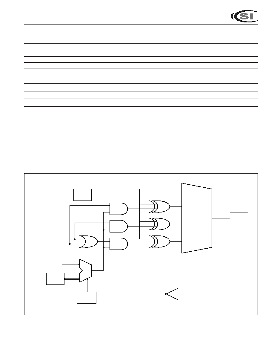
Enhanced Function
Port 4
Port 4, SFR P4 at address D8H, is a 4-bit multipurpose programmable I/O port. Each bit can be configured individually
by software. The Port 4 has four different operation modes.
In mode 0, P4.0~P4.3 is a bi-directional I/O port which is same as port 1. P4.2 and P4.3 also serve as external
interrupt
INT3
and
INT2
if enabled.
In mode 1, P4.0~P4.3 are read data strobe signals which are synchronized with beginning of read address signal at
specified address. These signals can be used as chip-select signals for external peripherals.
In mode 2, P4.0~P4.3 are write data strobe signals which are synchronized with beginning of written address signal at
specified address. These signals can be used as chip-select signals for external peripherals.
In mode 3, P4.0~P4.3 are write data strobe signals which are synchronized with beginning of read or written address
signal at specified address. These signals can be used as chip-select signals for external peripherals.
When Port 4 is configured with the feature of chip-select signals, the chip-select signal address range depends on the
contents of the SFRs P4xAH, P4xAL, P4CONA an P4CONB. The registers P4xAH and P4xAL contain the 16-bit base
address of P4.x. The registers P4CONA and P4CONB contain the control bits to configure the Port 4 operating mode.
Here is an example to program the P4.0 as a write strobe signal at the I/O port address 1234H~1237H and positive
polarity, and P4.1~P4.3 are used as general I/O ports.
MOV
P40AH,#12H
;Define the base I/O address 1234H for P4.0 as an special function pin.
MOV
P40AL,#34H
MOV
P4CONA,#00001010B
;Define the P4.0 as a write strobe signal pin and the compartor, length is 14.
MOV
P4CONB,#00H
;P4.1~P4.3 as general I/O port which are the same as Port 1.
MOV
P2ECON,#10H
;Write the P40SINV=1 to inverse the P4.0 write strobe polarity, default is
;negative.
Then any instruction MOVX @DPTR,A (with DPTR=1234H~1237H) will generate the positive polarity write strobe
signal at pin P4.0. And the instruction MOV P4,#XX will output the bit 3 to bit 1 of data #XX to pin P4.3~P4.1.
The SFRs of Port 4 are described in following. Figure 11 shows architecture of Port 4.
Port 4 base Address Registers : Reset values are 00000000B.
P40AH, P40AL(85H, 84H)
: The Base address register for comparator of P4.0. P40AH contains the high-order byte of
address, P40AL contains the low-order byte of address.
P41AH, P41AL(95H, 94H)
: The Base address register for comparator of P4.1. P41AH contains the high-order byte of
address, P41AL contains the low-order byte of address.
P42AH, P42AL(ADH, ACH)
: The Base address register for comparator of P4.2. P42AH contains the high-order byte of
address, P42AL contains the low-order byte of address.
P43AH, P43AL(B5H , B4H)
: The Base address register for comparator of P4.3. P43AH contains the high-order byte of
address, P43AL contains the low-order byte of address.
IC89E54/58/64
14
Integrated C ircuitSolution Inc.
MC012-0C 11/16/2001
P4CONB (C3H)
B7
B6
B5
B4
B3
B2
B1
B0
Flag Name
P43FUN1
P43FUN0
P43CMP1
P43CMP0
P42FUN1
P42FUN0
P42CMP1 P42CMP0
Bit
Name
Description
7,6
P43FUN1
=00: Mode 0. P4.3 is a general purpose I/O port which is the same as Port 1.
P43FUN0
=01: Mode 1. P4.3 is a Read Strobe Signal for chip selecting purpose. The address range depends
on the SFRs P43AH, P43AL and flags P43CMP1, P43CMP0.
=10: Mode 2. P4.3 is a Write Strobe Signal for chip selecting purpose. The address range depends
on the SFRs P43AH, P43AL and flags P43CMP1, P43CMP0.
=11: Mode 3. P4.3 is a Read/Write Strobe Signal for chip selecting purpose. The address range
depends on the SFRs P43AH, P43AL and flags P43CMP1, P43CMP0.
5.4
P43CMP1
Chip-select signals for address comparison.
P43CMP0
=00: Compare the full address (16 bits length) with the base address register P43AH, P43AL.
=01: Compare the 15 high bits (A15-A1) of address bus with the base address register
P43AH, P43AL.
=10: Compare the 14 high bits (A15-A2) of address bus with the base address register
P43AH, P43AL.
=01: Compare the 8 high bits (A15-A8) of address bus with the base address register
P43AH, P43AL.
3,2
P42FUN1
The P4.2 function control bits which are the similar definition as P42FUN1, P42FUN0.
P42FUN0
1,0
P42CMP1
The P4.2 address comparator length control bits which are the similar definition as P42CMP1,
P42CMP0
P42CMP0.
P4CONA (C2H)
B7
B6
B5
B4
B3
B2
B1
B0
Flag Name
P41FUN1
P41FUN0
P41CMP1
P41CMP0
P40FUN1
P40FUN0
P40CMP1
P40CMP0
Bit
Name
Description
7,6
P41FUN1
The P4.1 function control bits which are the similar definition as P41FUN1, P41FUN0.
P41FUN0
5,4
P41CMP1
The P4.1 address comparator length control bits which are the similar definition as P41CMP1,
P41CMP0
P41CMP0.
3,2
P40FUN1
The P4.0 function control bits which are the similar definition as P40FUN1, P40FUN0.
P40FUN0
1,0
P40CMP1
The P4.0 address comparator length control bits which are the similar definition as P40CMP1,
P40CMP0
P40CMP0.
IC89E54/58/64
Integrated C ircuitSolution Inc.
15
MC012-0C 11/16/2001
P4(D8H) :
B7
B6
B5
B4
B3
B2
B1
B0
Flag Name
-
-
-
-
P4.3
P4.2
P4.1
P4.0
Bit
Name
Description
7-4
-
These bits are reserved.
3
P4.3
Port 4 Data bit that output to pin P4.3 at mode 0.
2
P4.2
Port 4 Data bit that output to pin P4.2 at mode 0.
1
P4.1
Port 4 Data bit that output to pin P4.1 at mode 0.
0
P4.0
Port 4 Data bit that output to pin P4.0 at mode 0.
Figure 11. IC89E54/58/64 Port 4 Architecture
P4.x
P4xAL
P4xAH
P4xCMP0
P4xCMP1
ADDRESS BUS
WRITE ENABLE
READ ENABLE
P4xFUN0
P4xFUN1
PIN
P4.x
INPUT SIGNAL
DATA OUTPUT
RD_CS
WR_CS
RD/WR_CS
P4xCSINV

IC89E54/58/64
16
Integrated C ircuitSolution Inc.
MC012-0C 11/16/2001
P2ECON(AEH)
B7
B6
B5
B4
B3
B2
B1
B0
Flag Name
P43CSINV
P42CSINV
P41CSINV
P40CSINV
-
-
P2CN1
P2CN0
Bit
Name
Description
7
P43CSINV
The active polarity of P4.3 when pin P4.3 is defined as read/write strobe signal.
=1: P4.3 is active high when pin P4.3 is defined as read/write strobe signal.
=0: P4.3 is active low when pin P4.3 is defined as read/write strobe signal.
6
P42CSINV
The similarity definition as P43SINV.
5
P41CSINV
The similarity definition as P43SINV.
4
P40CSINV
The similarity definition as P43SINV.
3,2
-
Reserve
1,0
P2CN1,
=00 : Pin P2.7-P2.0 is the standard 8052 port 2.
P2CN0
=01 : Pins P2.7-P2.0 is input buffer port which the port enable address depends on the content
of P2EAL and P2EAH.
=10 : Pins P2.7-P2.0 is output-latched port which the port enable address depends on the
content of P2EAL and P2EAH.
=11 : Undefined.
Figure 12. IC89E54/58/64 Port 2 Architecture
74373
74244
PORT 2
P2EAL
P2EAH
PORT 2 OUTPUT DATA BUS
INTERNAL DATA BUS
P2CN1
P2CN0
PORT 2 INPUT DATA BUS
READ
WRITE
ADDRESS BUS
16-BIT
COMPARATOR
MUX
DEMUX
IC89E54/58/64
Integrated C ircuitSolution Inc.
17
MC012-0C 11/16/2001
AUXR(8EH)
:
Reset value is xxx0x000B.
B7
B6
B5
B4
B3
B2
B1
B0
Flag Name
-
-
-
ENARAM
-
OD1
OD0
ALED
Bit
Name
Description
7-5
-
These bits are reserved.
4
ENARAM
1, Enable AUX RAM.
3
-
These bits are reserved.
2-1
OD1-OD0
Select the delay periods of oscillation when waking up from power-down mode.
OD1 OD0
Delay Period
0
0
2,048 clock cycles (Default)
0
1
8,192 clock cycles
1
0
32,768clock cycles
1
1
131,072 clock cycles
0
ALED
1, Turn off ALE output while CPU accesses internal Flash memory.
P2EAH, P2EAL
: The Port Enable Address Registers for Port 2 is defined as input buffer like 74244, or an output-latched
logic like a 74373. The P2EAH contains the high-order byte of address, the P2EAL contains the low-order byte of address.
Figure 12 shows architecture of Port 2. The following example shows how to program the Port 2 as a output-latched port
at address 5678H.
MOV
P2EAL,#78H
;High-order byte of address to enable Port 2 latch function.
MOV
P2EAH,#56H
;Low-order byte of address to enable Port 2 latch function.
MOV
P2ECON,#02H
;Configure the port 2 as an output-latched port.
MOV
DPTR,#5678H
;Move data 5678H to DPTR.
MOV
A,#55H
MOVX
@DPTR,A
;The pins P2.7~P2.0 will output and latch the value 55H.
When Port 2 is configured as 74244 or 74373 function, the instruction "MOV P2,#XX" will write the data #XX to P2 register
only but not output to port pins P2.7~P2.0.
Power Down Mode
When the PD bit in the PCON register is set, the processor enters the power-down mode. In this mode, all of the clocks
are stopped, including the oscillator. To exit from power-down mode is by a hardware reset or external interrupts
INT0
to
INT3
when enabled and set to level triggered. To ensure that the oscillator is stable before the CPU restarts, the IC89E54/
58/64 series provide adjustable internal software delay counter. By the default, the device will experience a delay of 2048
clock cycles while the oscillation is recognized. The period of delay is selected by configuring the AUXR register bits OD0,
OD1 and OD2.
Reduce EMI Emission
Because of on-chip flash, when a program is running in internal program memory space, the ALE will be unused. The
transition of ALE will cause larger noise and EMI effect, so it can be turned off to reduce noise and EMI emission if it is
useless. Turning off the ALE signal transition only requires setting the bit 0 of the AUXR SFR, which is located at 08EH.
When ALE is turned off, it will be reactivated when the program accesses external ROM/RAM data or jumps to execute an
external ROM code. The ALE signal will turn off again after it has been completely accessed or program returns to internal
ROM code space. The ALED bit in the AUXR register, when set, disables the ALE output.

IC89E54/58/64
18
Integrated C ircuitSolution Inc.
MC012-0C 11/16/2001
Power Control Register
PCON(87H) :
B7
B6
B5
B4
B3
B2
B1
B0
Flag Name
SMOD
-
-
-
GF1
GF0
PD
IDL
Bit
Name
Description
7
SMOD
Double baud rate bit. If Timer 1 is used to generate baud rate and SMOD=1, the baud rate is
doubled when the serial port is used in modes 1, 2, or 3.
6-4
-
These bits are reserved.
3
GF1
General purpose flag bit.
2
GF0
General purpose flag bit.
1
PD
Power down bit. Setting this bit activates power down operation in the IC89E54/58/64.
0
IDL
Idle mode bit. Setting this bit activate idle mode operation in the 89E54/58/64.
If 1s are written to PD and IDL at the same time, PD takes precedence.

IC89E54/58/64
Integrated C ircuitSolution Inc.
19
MC012-0C 11/16/2001
FLASH MEMORY PROGRAMMING
The Flash architecture of IC89E54/58/64 is shown in Figure 13. IC89E54/58 include block 1 and lock bits block. The
signature bytes are fixed value reside in MCU, they are read only. Block 2 resides in IC89E64 only.
Figure 13. The Flash Architecture of IC89E54/58/64
EXTERNAL HOST MODE
The IC89E54/58/64 provide the user with a direct flash memory access that can be used for programming into the flash
memory without using the CPU. The direct flash memory access is entered using the External Host Mode. While the reset
input (RST) is continually held active (high), if the
PSEN
pin is forced by an input with low state, the device enters the External
Host Mode arming state at this time. The CPU core is stopped from running and all the chip I/O pins are reassigned and
become flash memory access and control pins. At this time, the external host should initiate a "Read Signature Bytes"
operation. After the completion of the "Read Signature Bytes" operation, the device is armed and enters the External Host
Mode. After the device enters into the External Host Mode, the internal flash memory blocks are accessed through the re-
assigned I/O port pins by an external host, such as a printed circuit board tester, a PC controlled development board or an
MCU programmer.
3 Lock Bits Flash Cell
3x8 bits
Signature Bytes
0030H
0032H
Dummy Address
16K Flash
( Block 1)
0000H
3FFFH
3 Lock Bits Flash Cell
3x8 bits
Signature Bytes
0030H
0032H
Dummy Address
32K Flash
( Block 1)
0000H
7FFFH
3 Lock Bits Flash Cell
3x8 bits
Signature Bytes
0030H
0032H
60K Flash
( Block 1)
0000H
EFFFH
4K Flash
( Block 2)
F000H
FFFFH
IC89E54
IC89E58
IC89E64
IC89E54/58/64
20
Integrated C ircuitSolution Inc.
MC012-0C 11/16/2001
When the chip is in the external host mode, Port 0 pins are assigned to be the parallel data input and output pins. Port
1 pins are assigned to be the low order address bus signals for the internal flash memory (A0-A7). The first six bits of Port
2 pins (P2[0:5]) are assigned to be the upper order address bus signals for the internal flash memory (A8-A13) along with
two of the Port 3 pins (P3.2 as A14 and P3.3 as A15). Two upper order Port 2 pins (P2.6 and P2.7) and two upper order
Port 3 pins (P3.6 and P3.7) along with RST,
PSEN
,
PROG
/ALE,
EA
pins are assigned as the control signal pins. The P3.
4 is assigned to be the ready/busy status signal, which can be used for handshaking with the external host during a flash
memory programming operation. The flash memory programming operation (Erase, Program, Verify, etc.) is internally self-
timed and can be controlled by an external host asynchronously or synchronously.
The insertion of an "arming" command prior to entering the External Host Mode by utilizing the "Read Signature Bytes"
operation provides additional protection for inadvertent writes to the internal flash memory cause by a noisy or unstable
system environment during the power-up or power unstable conditions.
The External Host Mode uses hardware setup mode, which are decoded from the control signal pins, to facilitate the
internal flash memory erase, test and programming process. The External Host Mode Commands are enabled on the falling
edge of ALE/
PROG
. The list in Table 4 outlines all the setup conditions of normal mode. Before entering these written
modes must have read 3 signature bytes.
Programming Interface
Some conditions must be satisfied before entering the programming mode. The conditions are listed in Table 4. The
interface-controlled signals are matched these conditions, then the IC89E54/58/64 will enter received command mode. The
flash command is accepted by the flash command decoder in command received mode. The programming interface is listed
in figure 14.
Figure 14. IC89E52/54/64 External Host Programming Signals
VSS
RST
PSEN
ALE/PROG
EA/VPP
H
L
PROG pulse
12V/H
VCC
IC
89E54/58/64
10K
VCC
D7-D0
P0
A7-A0
P3.4
P2.6
P2.7
P3.6
P3.7
Ready/Busy
P2.6
P2.7
P3.6
P3.7
A13-A8
A15-A14
P1
P2.5-2.0
P3.3-3.2
IC89E54/58/64
Integrated C ircuitSolution Inc.
21
MC012-0C 11/16/2001
Table 4. Flash Programming Mode
Mode
(1)
RST
PSEN PROG EA
P2.6
P2.7
P3.6
P3.7
P0[7:0] P1[7:0] P3[3:2]
COM
P2[5:0] HEX
(3)
Read Signature Byte
H
L
H
H
L
L
L
L
DO
AL
AH
0
Chip Erase
H
L
12V/H
H
L
L
L
X
X
X
1
Block 1
(2)
Erase
H
L
12V/H
L
H
L
L
X
X
X
2
Block 2
(2)
Erase
H
L
12V/H
L
L
H
L
X
X
X
4
Program Main code
H
L
12V/H
L
H
H
H
DI
AL
AH
E
Program Lock Bit 1
H
L
12V/H
H
H
H
H
X
X
X
F
Program Lock Bit 2
H
L
12V/H
H
H
L
L
X
X
X
3
Program Lock Bit 3
H
L
12V/H
H
L
H
L
X
X
X
5
Verify Lock Bits
H
L
H
H
H
L
L
H
DO[3:1]
X
X
9
Verify Main Code
H
L
H
H
L
L
H
H
DO
AL
AH
C
1. To read the signature bytes 30H, 31H, 32H are needed before any written command. To read signature bytes is needed
after any new mode changed. This operation provides additional protection for inadvertent writes to the internal flash
memory cause by a noisy or unstable system environment during the power-up or unstable power condition. If any
unstable power condition has happened while written operation proceeds, to read signature bytes again will re-enable
written command. (Power-on reset voltage is about 2.7V.)
2. Block 1 includes flash address from 0000H to 3FFFH in IC89E54, from 0000H to 7FFFH in IC89E58, from 0000H to
EFFFH in IC89E64. Block 2 includes F000H to FFFFH. Block 2 is resident in IC89E64 only.
3. "COM HEX" presents the combination value of [P3.7, P3.6, P2.7, P2.6].
Product Identification
The "Read Signature Bytes" command accesses the Signature Bytes that identify the device as IC89E54/58/64 and the
manufacturer code. External programmers primarily use these Signature Bytes, shown in Table 4, in the selection of
programming algorithms. The Read Signature Bytes command is selected by the byte code of 00h on P3[7:6] and P2[7:
6]. Manufacturer code of ICSI is "D5H" that reside in address 30H of signature. The flash memory sizes of MCU are shown
in address 31H, code value 04H respect to 16K main flash memory, code value 08H respect to 32K main flash memory,
code value 10H respect to 64K main flash memory. The address 32H value of signature byte respect to written operation
VPP value, code value FFH respects to 12V and 55H respects to 5V.
Table 5. Signature Bytes Information
Addr 30H
Addr 31H
Addr 32H
IC89E54 (VPP=12V)
D5H
04H
FFH
IC89E54 (VPP=5V)
D5H
04H
05H
IC89E58 (VPP=12V)
D5H
08H
FFH
IC89E58 (VPP=5V)
D5H
08H
05H
IC89E64 (VPP=12V)
D5H
10H
FFH
IC89E64 (VPP=5V)
D5H
10H
05H

IC89E54/58/64
22
Integrated C ircuitSolution Inc.
MC012-0C 11/16/2001
Arming Command
An arming command must take place before a Written Mode will be recognized by the IC89E54/58/64. This is to prevent
accidental triggering of written operation due to noise or programmer error. The arming command is as follows:
A Read Signature Bytes command is issued. This is actually a natural step for the programmer, but will also serve as
the arming command. After the above sequence, all other Written Mode commands are enabled. Before the Read Signature
Bytes command is received, all other Written Mode commands received are ignored. The IC89E54/8/64 will exit Written
Mode if power off, so arming command is needed every power on for entering External Host Command Mode.
External Host Mode Commands
The following is a brief description of the commands. See Table 4 for all signal logic assignments for the External Host
Mode Commands. The critical timing for all Erase and Program commands, is self-generated by the flash memory controller
on-chip.
The high-to-low transition of the
PROG
signal initiates the Erase and Program commands, which are synchronized
internally. All the data in the memory array will be erased to FFH. Memory addresses that are to be programmed must be
in the erased state prior to programming. Selection of the Erase command to use, prior to programming the device, will be
dependent upon the contents already in the array and the desired programming field block.
The "Chip Erase" command erases all bytes in both memory blocks of the IC89E54/58/64.This command ignores the
"Lock bits" status and will erase the Security Byte. The "Chip Erase" command is selected by the byte code of 01H on P3
[7:6] and P2[7:6].
Flash Operation Status Detection (Ext. Host Handshake)
The IC89E54/58/64 provide two signals mean for an external host to detect the completion of a flash memory
operation, therefore the external host can optimize the system Program or Erase cycle of the embedded flash memory.
The end of a flash memory operation cycle (Erase or Program) can be detected by monitoring the Ready/
Busy
bit at
Port 3.4. The following two Program commands are for programming new data into the memory array. Selection of
which Program command to use for programming will be dependent upon the desired programming field size. The
Program commands will not enable if the Lock bit 2 or Lock Bit 3 is enabled on the selected memory block. The
"Program Main Code" command program data into a single byte. Ports P0[0:7] are used for data in. The memory
location is selected by P1[0:7], P2[0:5], and P3[2:3] (A0-A15). The "Program Main Code" command is selected by the
byte code on P3[6:7] and P2[6:7].
The "Verify Main Code" command allows the user to verify that the IC89E54/58/64 correctly performed an Erase or
Program command. Ports P0[0:7] are used for data out. The memory location is selected by P1[0:7], P2[0:5], and P3[2:3]
(A0-A15). These commands will not enable if any lock bit is enabled on the selected memory block.
Ready/
Busy
Busy
Busy
Busy
Busy
The progress of the flash memory programming can be monitored by the Ready/
Busy
output signal. The Ready/
Busy
indicates whether an Embedded Algorithm in Written State Machine (WSM) is in progress or complete. The RY/
BY
status
is valid after the falling edge of the programming or erase controlled signal. If the output is low (Busy), the device is in an
erasing/programming state with an internal verification. If the output is high, the device is ready to read data. If Ready/
Busy
signal doesn't generate a low pulse or doesn't return from low to high in an expected time, the programming/erasing action
will be failed.

IC89E54/58/64
Integrated C ircuitSolution Inc.
23
MC012-0C 11/16/2001
Programming a IC89E54/58/64
To program new data into the memory array, supply 5 volts to VDD and RST, and perform the following steps.
1. Set RST to high and
PSEN
to low.
2. Read the "Read Signature Bytes" command to ensure the correct programming algorithm.
3. Raise
EA
High (either 12V or 5V).
4. Verify that the memory blocks for programming are in the erased state, FFH. If they are not erased, then erase them
using the Chip Erase command. (Chip Erase operation will have a Ready/
Busy
signal output from P3.4, if Ready/
Busy
signal doesn't return from low to high in 7.2 sec, the Chip Erase operation will be failed.)
5. Set P2.6, P2.7, P3.6, P3.7 to a properly programming combination.
6. Select the memory location using the address lines (P1[0:7], P2[0:5], P3[2:3]).
7. Present the data in on P0[0:7].
8. Pulse ALE/
PROG
.
9. Wait for low to high transition on Ready/
Busy
(P3.4). If Ready/
Busy
is from low to high, this address is programmed
completely. If Ready/
Busy
pin don't return from low to high in 720us while programming one byte, the Programming
operation will be failed.
10. Repeat steps 6~9 until programming is finished.
Lock bits Features
The IC89E54/58/64 provide three lock bits to protect the embedded program against software piracy. These three
bytes are user programmable. The relation between lock bits status and protection type are listed in table 6.
Program Lock bits
Protection in Normal Mode
LB1
LB2
LB3
1
U
U
U
No program lock feature enabled.
2
P
U
U
MOVC instructions executed from external program memory are
disabled from fetching code bytes from internal memory,
EA
is
sampled and latched on reset, and Data verification is disabled.
("Verify Signature Byte" and "Verify Lock Bits are still enabled.)
3
P
P
U
Same as 2, also further written operation of the Flash is disabled
4
P
P
P
Same as 3, also external execution is disabled.
Table 6. Lock Bits Features
Special Issue
There are two conditions must be sure. One is P2.6 and P2.7 can not be low levels when RST pin falling edge. Another
is P4.3 can not be low level while RST falling edge. One of upper case is generate, the program will not be executing
correctly.

IC89E54/58/64
24
Integrated C ircuitSolution Inc.
MC012-0C 11/16/2001
OPERATING RANGE
(1)
Range
Ambient Temperature
V
CC
Oscillator Frequency
Commercial
0∞C to +70∞C
+4.5V to +5V
3.5 to 40 MHz
Note:
1. Operating ranges define those limits between which the functionality of the device is guaranteed.
ABSOLUTE MAXIMUM RATINGS
Parameter
Rating
Unit
Operating Temperature Under Bias
0 to +70
∞C
(1)
Storage Temperature Range
≠65 to +125
∞C
Voltage on any other pin to Vss
≠2.0 to +7.0
V
(2)
Power Dissipation (Based on package heat
1.5
W
transfer limitations, not device power consumption)
Note:
1. Operating temperature is for commercial products defined by this specification.
2. Minimum DC input voltage is ≠0.5V. During transitions, inputs may undershoot to ≠2.
0V for periods less than 20 ns. Maximum DC voltage on output pins is Vcc + 0.5V
which may overshoot to Vcc + 2.0V for periods less than 20 ns.
IC89E54/58/64
Integrated C ircuitSolution Inc.
25
MC012-0C 11/16/2001
DC CHARACTERISTICS
( Ta = 0∞C to 70∞C; VCC = 5V+10% ; VSS = 0V )
Symbol
Parameter
Test conditions
Min
Max
Unit
V
IL
Input low voltage
≠0.5
0.2Vcc ≠ 0.1
V
V
IL
1
Input low voltage (XTAL1,
EA
)
≠0.5
0.2Vcc ≠ 0.3
V
V
IH
Input high voltage
0.2Vcc + 0.9
Vcc + 0.5
V
(except XTAL 1, RST,
EA
)
V
IH
1
Input high voltage (XTAL 1,
EA
)
0.7Vcc
Vcc + 0.5
V
V
SCH
+
RST positive schmitt-trigger
0.7Vcc
Vcc + 0.5
V
threshold voltage
V
SCH
≠
RST negative schmitt-trigger
0
0.3Vcc
V
threshold voltage
V
OL
(1)
Output low voltage
Iol = 100 µA
--
0.3
V
(Ports 1, 2, 3)
I
OL
= 1.6 mA
--
0.45
V
I
OL
= 3.5 mA
--
1.0
V
V
OL
1
(1)
Output low voltage
I
OL
= 200 µA
--
0.3
V
(Port 0, ALE,
PSEN
)
I
OL
= 3.2 mA
--
0.45
V
I
OL
= 7.0 mA
--
1.0
V
V
OH
Output high voltage
I
OH
= ≠10 µA
0.9Vcc
--
V
(Ports 1, 2, 3, ALE,
PSEN
)
Vcc = 4.5V ~ 5.5V
I
OL
= ≠25 µA
0.75Vcc
--
V
I
OL
= ≠60 µA
2.4
--
V
V
OH
1
Output high voltage
I
OH
= ≠80 µA
0.9Vcc
--
V
(Port 0, ALE,
PSEN
)
Vcc = 4.5V ~ 5.5V
I
OH
= ≠300 µA
0.75Vcc
--
V
I
OH
= ≠800 µA
2.4
--
V
I
IL
Logical 0 input current (Ports 1, 2, 3) V
IN
= 0.45V
--
≠50
µA
I
LI
Input leakage current (Port 0)
V
IN
= 0.45V or Vcc
≠10
+10
µA
I
TL
Logical 1-to-0 transition current
V
IN
= 2.0V
--
≠650
µA
(Ports 1, 2, 3)
R
RST
RST pulldown resister
V
IN
= 0V
50
300
K
Note:
1. Under steady state (non-transient) conditions, I
OL
must be externally limited as follows:
Maximum I
OL
per port pin:
10 mA
Maximum I
OL
per 8-bit port
Port 0: 26 mA
Ports 1, 2, 3: 15 mA
Maximum total I
OL
for all output pins: 71 mA
If I
OL
exceeds the test condition, V
OL
may exceed the related specification.
Pins are not guaranteed to sink greater than the listed test conditions.
IC89E54/58/64
26
Integrated C ircuitSolution Inc.
MC012-0C 11/16/2001
POWER SUPPLY CHARACTERISTICS
Symbol
Parameter
Test conditions
Min
Max
Unit
Icc
Power supply current
(1)
Vcc=5.0V
Active mode
12 MHz
--
20
mA
16 MHz
--
26
mA
20 MHz
--
32
mA
24 MHz
--
38
mA
32 MHz
--
50
mA
40 MHz
--
62
mA
Idle mode
12 MHz
--
5
mA
16 MHz
--
6
mA
20 MHz
--
7.6
mA
24 MHz
--
9
mA
32 MHz
--
12
mA
40 MHz
--
15
mA
Power-down mode
Vcc=5.0V
--
50
µA
Note:
1. The I
CC
test conditions are shown below. Minimum V
CC
for Power Down is 2 V.
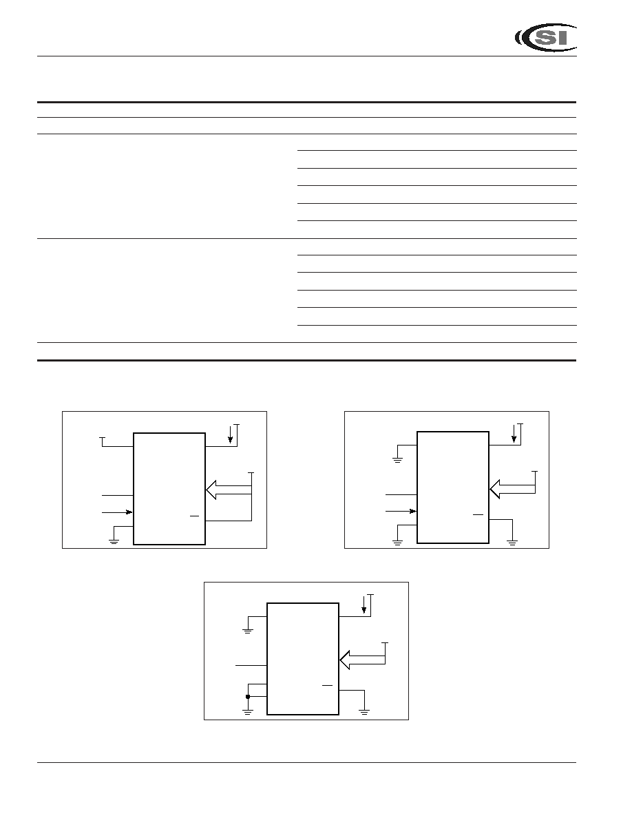
Figure 15. Active Mode
Figure 16. Idle Mode
Figure 17. Power Mode
(V
CC
=2.0V~6.0V)
XTAL1
GND
NC
RST
Vcc
P0
EA
Vcc
Vcc
CLOCK
SIGNAL
Icc
XTAL2
Vcc
XTAL1
GND
NC
RST
Vcc
P0
EA
Vcc
Vcc
CLOCK
SIGNAL
Icc
XTAL2
XTAL1
GND
NC
RST
Vcc
P0
EA
Vcc
Vcc
Icc
XTAL2
IC89E54/58/64
Integrated C ircuitSolution Inc.
27
MC012-0C 11/16/2001
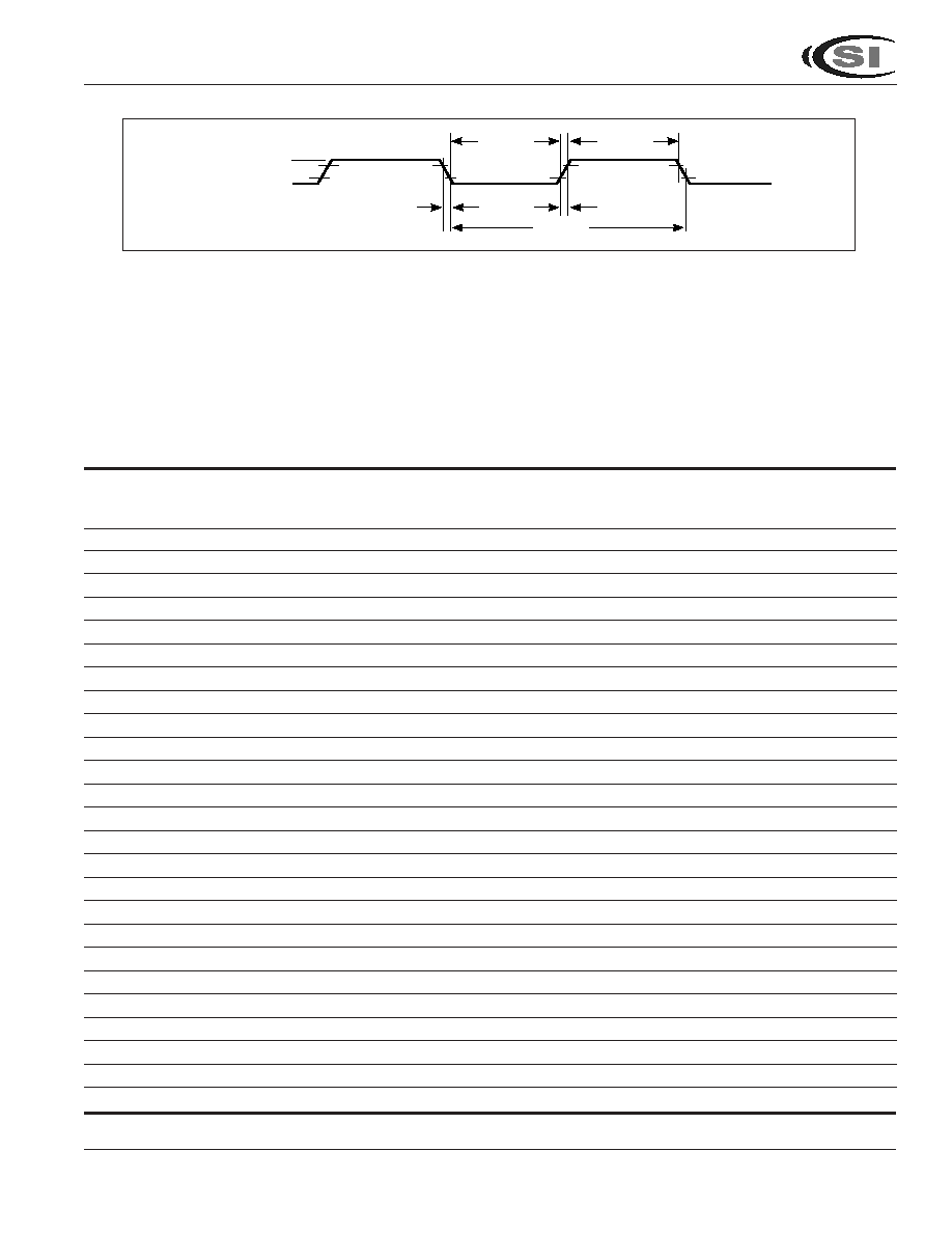
Figure 18. Clock Singal Waveform for Icc Tests in Active and Idle Mode (t
CLCH
=t
CHCL
=5 ns)
AC CHARACTERISTICS
(Ta=0∞Cto 70∞C; VCC=5V 10%; V
SS
=0V; C1 for port 0, ALE and
PSEN
Outputs=100pF; C1 for other outputs=80pF)
EXTERNAL MEMORY CHARACTERISTICS
24 MHz
40 MHz
Variable Oscillator
Clock
Clock
(3.5 - 40 MHz)
Symbol
Parameter
Min
Max
Min Max
Min
Max
Unit
1/t
CLCL
Oscillator frequency
--
--
--
--
3.5
40
MHz
t
LHLL
ALE pulse width
68
--
35
--
2t
CLCL
≠15
--
ns
t
AVLL
Address valid to ALE low
26
--
10
--
t
CLCL
≠15
--
ns
t
LLAX
Address hold after ALE low
31
--
15
--
t
CLCL
≠10
--
ns
t
LLIV
ALE low to valid instr in
--
147
--
80
--
4t
CLCL
≠20
ns
t
LLPL
ALE low to
PSEN
low
31
--
15
--
t
CLCL
≠10
--
ns
t
PLPH
PSEN
pulse width
110
--
60
--
3t
CLCL
≠15
--
ns
t
PLIV
PSEN
low to valid instr in
--
105
--
55
--
3t
CLCL
≠20
ns
t
PXIX
Input instr hold after
PSEN
0
--
0
--
0
--
ns
t
PXIZ
Input instr float after
PSEN
--
37
--
20
--
t
CLCL
≠5
ns
t
AVIV
Address to valid instr in
--
188
--
105
--
5t
CLCL
≠20
ns
t
PLAZ
PSEN
low to address float
--
10
--
10
--
10
ns
t
RLRH
RD
pulse width
230
--
130
--
6t
CLCL
≠20
--
ns
t
WLWH
WR
pulse width
230
--
130
--
6t
CLCL
≠20
--
ns
t
RLDV
RD
low to valid data in
--
157
--
90
--
4t
CLCL
≠10
ns
t
RHDX
Data hold after
RD
0
--
0
--
0
--
ns
t
RHDZ
Data float after
RD
--
78
--
45
--
2t
CLCL
≠5
ns
t
LLDV
ALE low to valid data in
--
282
--
165
--
7t
CLCL
≠10
ns
t
AVDV
Address to valid data in
--
323
--
190
--
8t
CLCL
≠10
ns
t
LLWL
ALE low to
RD
or
WR
low
105
145
55
95
3t
CLCL
≠20
3t
CLCL
+20
ns
t
AVWL
Address to
RD
or
WR
low
146
--
80
--
4t
CLCL
≠20
--
ns
t
QVWX
Data valid to
WR
transition
26
--
10
--
t
CLCL
≠15
--
ns
t
WHQX
Data hold after
WR
31
--
15
--
t
CLCL
≠10
--
ns
t
RLAZ
RD
low to address float
--
0
--
0
--
0
ns
t
WHLH
RD
or
WR
high to ALE high
26
57
10
40
t
CLCL
≠15
t
CLCL
+15
ns
0.45V
Vcc --
0.5V
t
CHCX
t
CLCL
t
CLCH
t
CLCX
t
CHCL
0.7Vcc
0.2Vcc --
0.1

IC89E54/58/64
28
Integrated C ircuitSolution Inc.
MC012-0C 11/16/2001
SERIAL PORT TIMING: SHIFT REGISTER MODE
24 MHz
40 MHz
Variable Oscillator
Clock
Clock
(3.5-40 MHz)
Symbol
Parameter
Min
Max
Min Max
Min
Max
Unit
t
XLXL
Serial port clock cycle time
490
510
290 310
12t
CLCL
≠10
12t
CLCL
+10
ns
t
QVXH
Output data setup to
406
--
240
--
10t
CLCL
≠10
--
ns
clock rising edge
t
XHQX
Output data hold after
73
--
40
--
2t
CLCL
≠10
--
ns
clock rising edge
t
XHDX
Input data hold after
0
--
0
--
0
--
ns
clock rising edge
t
XHDV
Clock rising edge to
--
417
--
250
--
10t
CLCL
ns
input data valid
EXTERNAL CLOCK DRIVE CHARACTERISTICS
Symbol
Parameter
Min
Max
Unit
1/t
CLCL
Oscillator Frequency
3.5
40
MHz
t
CHCX
High time
10
--
ns
t
CLCX
Low time
10
--
ns
t
CLCH
Rise time
--
10
ns
t
CHCL
Fall time
--
10
ns
IC89E54/58/64
Integrated C ircuitSolution Inc.
29
MC012-0C 11/16/2001
Flash Program/Erase and Verification & Test Mode Characteristics
Symbol
Parameter
Min
Max
Unit
Vpph
Programming and Erase Enable Voltage
11.5
12.5
V
Vppl
Programming and Erase Enable Voltage
4.5
6.0
V
Ipph
Programming and Erase Enable Current while VPP=Vpph
-
2.0
mA
Ippl
Programming and Erase Enable Current while VPP=Vppl
-
1.0
mA
tWSCV
Power Setup to Command Setup Low
10
-
ms
tCVQV
Command Valid to Data Output Valid
-
60
ns
tAVQV
Address Valid to Data Output Valid
-
60
ns
tCVPL
Command Valid to
PROG
Low
30
-
ns
tSHPL
VPP Setup to
PROG
Low
30
-
ns
tAVPL
Address Setup to
PROG
Low
30
-
ns
tDVPL
Data Setup to
PROG
Low
30
-
ns
tPLBL
PROG
Low to
Bus
y Low
1
10
us
tBLCX
Command Hold after
Busy
Low
30
-
ns
tBLAX
Address Hold after
Busy
Low
30
-
ns
tBLPH
Busy
Low to
PROG
high
30
-
ns
tBLDX
Data Hold after
Busy
Low
30
-
us
tBLBH
Busy
Low to
Busy
High
15
480
us
tBHSL
VPP Hold after
Busy
High
1
-
us
tAXQX
Output Hold after Address Release
0
-
ns
tCXQX
Output Hold after Command Release
0
-
ns
tBLBHE
Busy
Time while Chip Erase
-
4.5
Sec
tBLBHE1
Busy
Time while Block 1 Erase (IC89E54)
-
1.2
Sec
tBLBHE2
Busy
Time while Block 1 Erase (IC89E58)
-
2.4
Sec
tBLBHE3
Busy
Time while Block 1 Erase (IC89E64)
-
4.0
Sec
tBLBHE4
Busy
Time while Block 2 Erase (IC89E64)
-
0.7
Sec
IC89E54/58/64
30
Integrated C ircuitSolution Inc.
MC012-0C 11/16/2001
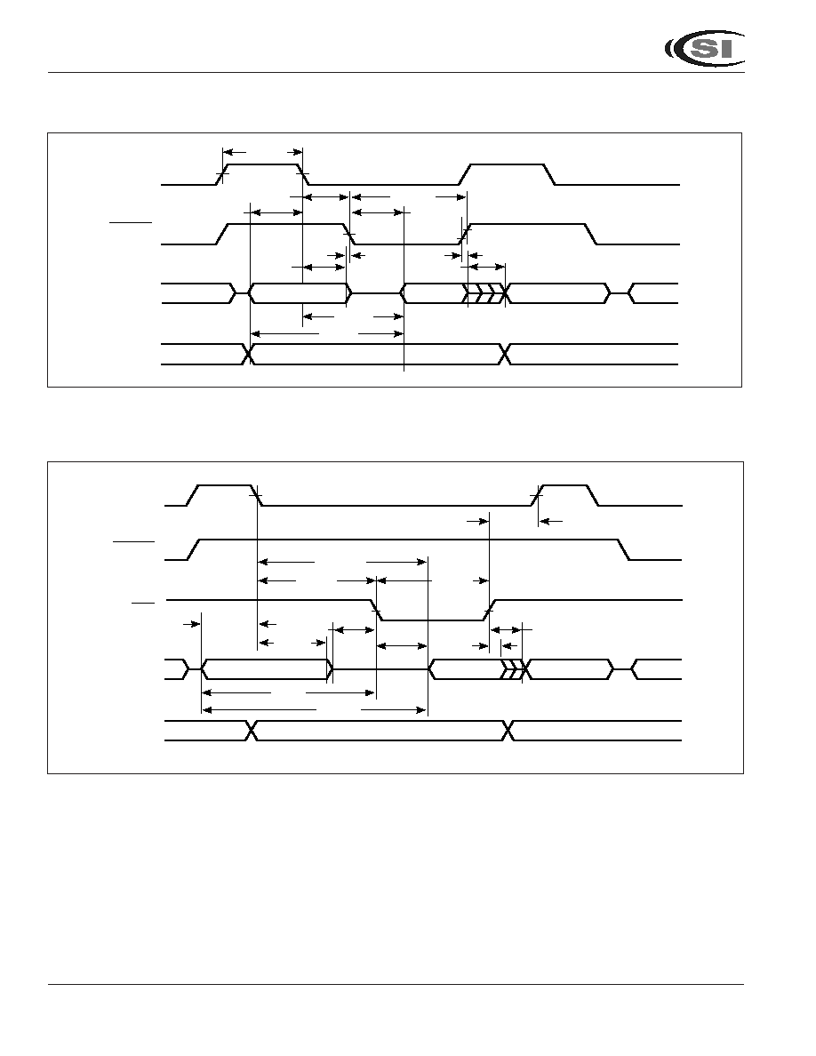
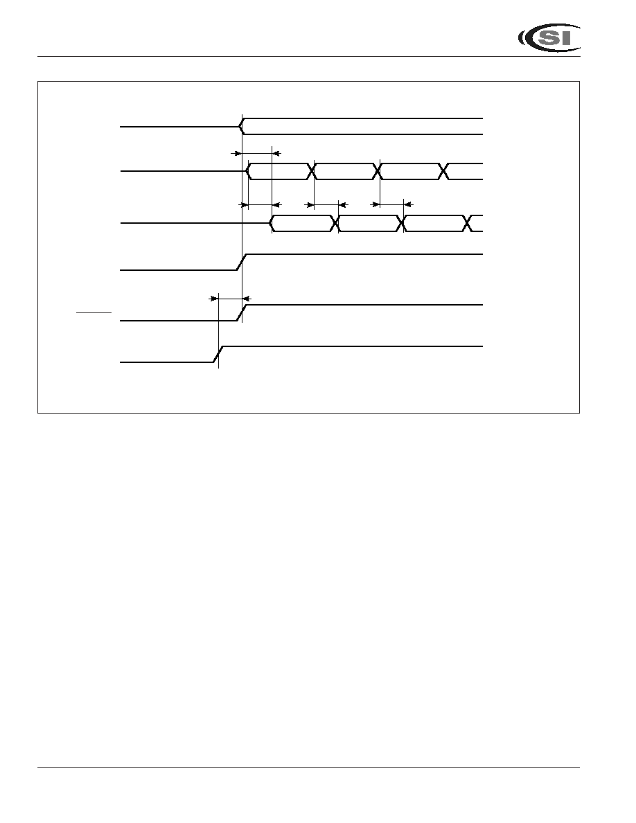
Figure 19. External Program Memory Read Cycle
Figure 20. External Data Memory Read Cycle
TIMING WAVEFORMS
t
LHLL
ALE
t
AVLL
t
LLPL
t
PLPH
t
PLIV
t
LLAX
t
PLAZ
t
PXIZ
t
PXIX
A7-A0
INSTR IN
A7-A0
t
LLIV
t
AVIV
PSEN
PORT 0
PORT 2
A15-A8
A15-A8
t
LLDV
t
AVLL
A7-A0 FROM RI OR DPL
INSTR IN
A7-A0 FROM PCL
t
AVWL
t
AVDV
PSEN
PORT 0
PORT 2
ALE
RD
DATA IN
A15-A8 FROM DPH
A15-A8 FROM PCH
t
WHLH
t
LLWL
t
LLAX
t
RLAZ
t
RLDV
t
RHDZ
t
RHDX
t
RLRH
IC89E54/58/64
Integrated C ircuitSolution Inc.
31
MC012-0C 11/16/2001
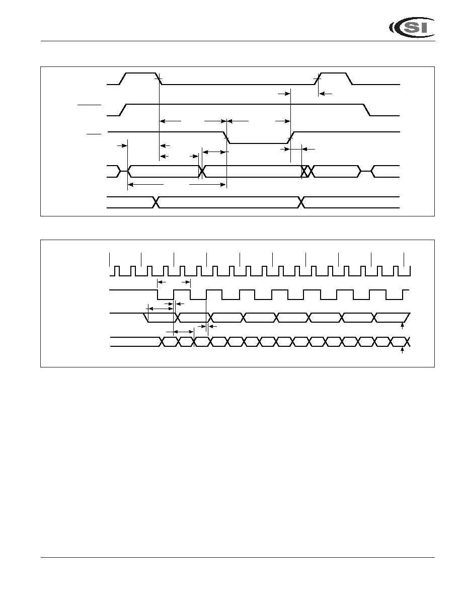
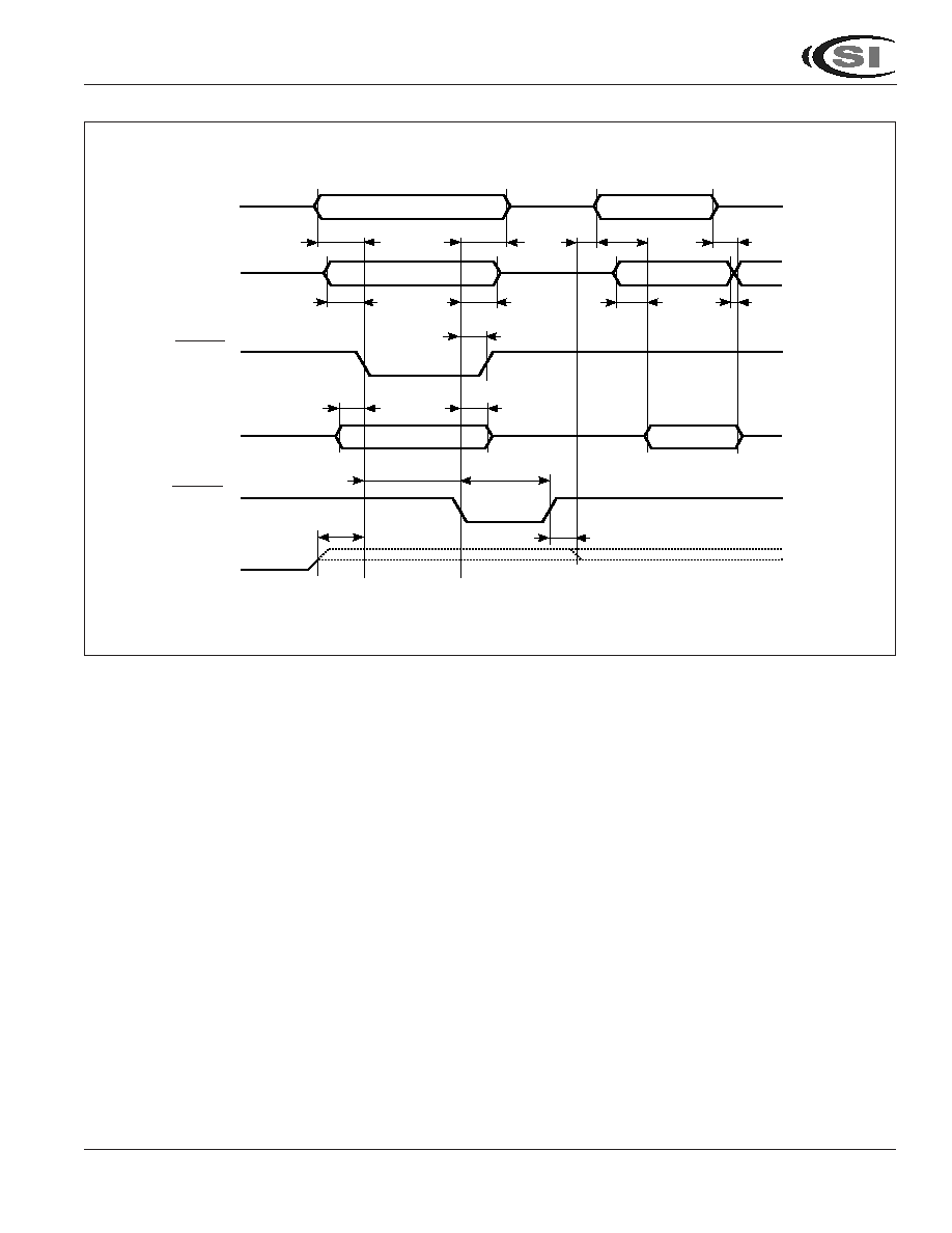
Figure 21. External Data Memory Write Cycle
Figure 22. Shift Register Mode Timing Waveform
t
AVLL
A7-A0 FROM RI OR DPL
INSTR IN
A7-A0 FROM PCL
t
AVWL
PSEN
PORT 0
PORT 2
ALE
WR
DATA OUT
A15-A8 FROM DPH
A15-A8 FROM PCH
t
WHLH
t
LLWL
t
LLAX
t
QVWX
t
WHQX
t
WLWH
INSTRUCTION
ALE
CLOCK
DATA
OUT
DATA
IN
t
XLXL
t
XHQX
t
QVXH
t
XHDV
t
XHDX
VALID
VALID
VALID
VALID
VALID
VALID
VALID
VALID
SET TI
SET RI
7
8
6
5
4
3
2
1
0
7
6
5
4
3
2
1
0
IC89E54/58/64
32
Integrated C ircuitSolution Inc.
MC012-0C 11/16/2001
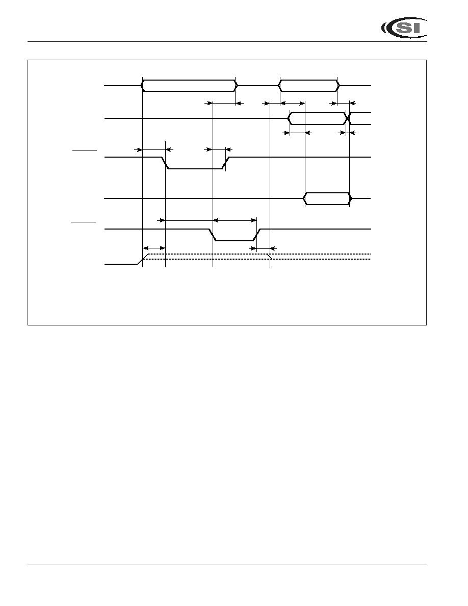
Figure 23. Read Signature bytes Timing(Arming Command)
P3[7:6]
P2[7:6]
PROG
VCC
t
CVQV
00H
30H
31H
P3[3:2]
P2[5:0]
P1[7:0]
P0[7-0]
VPP
t
WSCV
D5H
04H/08H/10H
05H/FFH
t
AVQV
t
AVQV
t
AVQV
32H
IC89E54/58/64
Integrated C ircuitSolution Inc.
33
MC012-0C 11/16/2001
Figure 24. Programming Timing
P3[7:6]
P2[7:6]
VPP
t
CVPL
t
BLCX
t
PLBL
t
BLBH
t
SHPL
t
BHSL
t
BLAX
t
CQCV
t
SLCV
t
CXQX
0CH/0DH
(2)
0EH
(1)
P3[3:2]
P2[5:0]
P1[7:0]
PROG
P0[7-0]
P3.4(BUSY)
t
AVPL
t
BLDX
t
AVQV
t
AXQX
Valid Address
(3)
Valid Address
(3)
t
BLPH
t
DVPL
Valid Data
(4)
Valid Data
Note:
1. 0EH is for code memory programming . In lock bits programming, 0FH, 03H, 05H respect to lock bit 1, 2, 3.
2. 0CH is for code memory verification and 0DH is for concurrent memory verification. 09H is for Lock bits verification.
3. Address don't care while lock bits' programming or verification.
4. Data don't care while lock bits' programming.
IC89E54/58/64
34
Integrated C ircuitSolution Inc.
MC012-0C 11/16/2001
Figure 25. Erasing Timing
P3[7:6]
P2[7:6]
VPP
t
CVPL
t
BLCX
t
PLBL
t
BLBHE
t
BLBHEn
t
SHPL
t
BHSL
t
CQCV
t
SLCV
t
CXQX
0CH/0DH
(2)
01H/02H/04H
(1)
P3[3:2]
P2[5:0]
P1[7:0]
PROG
P0[7-0]
P3.4(BUSY)
t
AVQV
t
AXQX
Valid Address
(3)
t
BLPH
Valid Data
Note:
1. 01H/02H/04H are for code Chip Erase/Block 1 Erase/Block2 Erase.
2. 0CH is for code memory verification. 09H is for Lock bits verification.

IC89E54/58/64
Integrated C ircuitSolution Inc.
35
MC012-0C 11/16/2001
Figure 26. Test Mode Entering Timing
Figure 27. External Clock Drive Waveform
Figure 28. AC Test Point
Note:
1.AC inputs during testing are driven at Vcc-0.5v for logic "1" and 0.45V for logic "0".
Timing measurements are made at Vih min for logic "1" and max for logic "0".
t
CVSL
t
PHCH
t
SLSH
1st stage
test mode
enable
2rd stage
test mode
enable
59H
59H
89H
89H
P2.6
P0[7-0]
0.45V
Vcc -- 0.5V
t
CHCX
t
CLCL
t
CLCH
t
CLCX
t
CHCL
0.7Vcc
0.2Vcc -- 0.1
Vcc - 0.5V
0.45V
0.2Vcc + 0.9V
0.2Vcc - 0.1V
Note:
1. EA, PROG, P3.7, P2.7 are high level; P3.6 is lower level.

IC89E54/58/64
36
Integrated C ircuitSolution Inc.
MC012-0C 11/16/2001
ORDERING INFORMATION
Commercial Range: 0∞C to +70∞C
Speed
Order Part Number
Package
12 MHz
IC89E54/58/64-12PL
PLCC
IC89E54/58/64-12W
600mil DIP
IC89E54/58/64-12PQ
PQFP
24 MHz
IC89E54/58/64-24PL
PLCC
IC89E54/58/64-24W
600mil DIP
IC89E54/58/64-24PQ
PQFP
40 MHz
IC89E54/58/64-40PL
PLCC
IC89E54/58/64-40W
600mil DIP
IC89E54/58/64-40PQ
PQFP
Integrated C ircuitSolution Inc.
HEADQUARTER:
NO.2, TECHNOLOGY RD. V, SCIENCE-BASED INDUSTRIAL PARK,
HSIN-CHU, TAIWAN, R.O.C.
TEL: 886-3-5780333
Fax: 886-3-5783000
BRANCH OFFICE:
7F, NO. 106, SEC. 1, HSIN-TAI 5
TH
ROAD,
HSICHIH TAIPEI COUNTY, TAIWAN, R.O.C.
TEL: 886-2-26962140
FAX: 886-2-26962252
http://www.icsi.com.tw