 | –≠–ª–µ–∫—Ç—Ä–æ–Ω–Ω—ã–π –∫–æ–º–ø–æ–Ω–µ–Ω—Ç: ICS309RIT | –°–∫–∞—á–∞—Ç—å:  PDF PDF  ZIP ZIP |

ICS309
MDS 309 G
1
Revision 122704
I n t e gra t e d C i r c u i t S y s t e m s
5 2 5 R a c e S t r e e t , S a n J o s e, C A 9 5 1 2 6
t e l ( 4 0 8 ) 2 9 7 - 1 2 0 1
w w w. i c s t . c o m
S
ERIAL
P
ROGRAMMABLE
T
RIPLE
PLL SS V
ERSA
C
LOCK
S
YNTHESIZER
Description
The ICS309 is a versatile serially-programmable, triple
PLL with spread spectrum clock source. The ICS309
can generate any frequency from 250kHz to 200 MHz,
and up to 6 different output frequencies simultaneously.
The outputs can be reprogrammed on-the-fly, and will
lock to a new frequency in 10 ms or less.
To reduce system EMI emissions, spread spectrum is
available that supports modulation frequencies of
31 kHz and 120 kHz, as well as modulation amplitudes
of +/-0.25% to +/-2.0%. Both center and down-spread
options are available.
The device includes a PDTS pin which tri-states the
output clocks and powers down the entire chip.
The ICS309 default for non-programmed start-up are
buffered reference clock outputs on all clock output
pins.
ICS' VersaClock
TM
programming software allows the
user to configure up to 9 outputs with target
frequencies, spread spectrum capabilities or buffered
reference clock outputs. The VersaClock
TM
software
automatically configures the PLLs for optimal overall
performance.
Features
∑
Packaged in 20-pin SSOP (QSOP)
∑
Highly accurate frequency generation
∑
M/N Multiplier PLL: M = 1..2048, N = 1..1024
∑
Serially programmable: user determines the output
frequency via a 3-wire interface
∑
Spread Spectrum frequency modulation for reduced
system EMI
∑
Center or Down Spread up to 4% total
∑
Selectable 32 kHz and 120 kHz modulation
∑
Eliminates need for custom quartz oscillators
∑
Input crystal frequency of 5 - 27 MHz
∑
Input clock frequency of 3 - 50 MHz
∑
Output clock frequencies up to 200 MHz
∑
Operating voltage of 3.3 V
∑
Up to 9 reference clock outputs
∑
Power down tri-state mode
∑
Very low jitter
Block Diagram
C rystal
O sc illator
P LL1 w ith
S pread
S pectrum
G N D
2
3
V DD
P D T S
P LL2
P LL3
Divide
Logic
and
Output
Enable
Control
CLK1
CLK9
CLK8
CLK7
CLK6
CLK5
CLK4
CLK3
CLK2
X 2
C rystal or
clock input
E xternal capacitors are
required w ith a crystal input.
X 1/IC LK
SCLK
DATA
STROBE
S
ERIAL
P
ROGRAMMABLE
T
RIPLE
PLL SS V
ERSA
C
LOCK
S
YNTHESIZER
MDS 309 G
2
Revision 122704
I n t e gr a t e d C i r c u i t S y s t e m s
5 2 5 R a c e S t r e e t , S a n J o s e, C A 9 5 1 2 6
t e l ( 4 0 8 ) 2 9 7 - 1 2 0 1
w w w. i c s t . c o m
ICS309
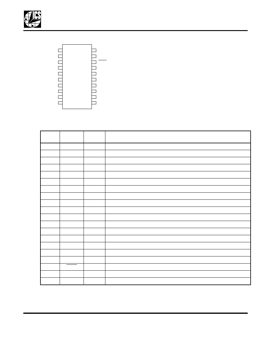
Pin Assignment
Pin Descriptions
16
1
15
2
14
D A T A
S T R O B E
3
13
X 2
4
12
X 1 /IC LK
S C LK
5
11
C LK 9
6
P D T S
7
V D D
8
G N D
V D D
V D D
G N D
C LK 1
C LK 5
C LK 2
C LK 6
9
10
C LK 3
C LK 7
C LK 4
C LK 8
20
19
18
17
20 pin (150 m il) SSOP (QSOP)
Pin
Number
Pin
Name
Pin
Type
Pin Description
1
DATA
Input
Serial data input.
2
X2
XO
Crystal Output. Connect this pin to a crystal. Float for clock input.
3
X1/ICLK
XI
Connect this pin to a crystal or external clock input.
4
CLK9
Output
Output clock 9. Default of Reference frequency output when unprogrammed.
5
VDD
Power
Connect to +3.3V.
6
GND
Power
Connect to Ground.
7
CLK1
Output
Output clock 1. Default of Reference frequency output when unprogrammed.
8
CLK2
Output
Output clock 2. Default of Reference frequency output when unprogrammed.
9
CLK3
Output
Output clock 3. Default of Reference frequency output when unprogrammed.
10
CLK4
Output
Output clock 4. Default of Reference frequency output when unprogrammed.
11
CLK8
Output
Output clock 8. Default of Reference frequency output when unprogrammed.
12
CLK7
Output
Output clock 7. Default of Reference frequency output when unprogrammed.
13
CLK6
Output
Output clock 6. Default of Reference frequency output when unprogrammed.
14
CLK5
Output
Output clock 5. Default of Reference frequency output when unprogrammed.
15
GND
Power
Connect to Ground.
16
VDD
Power
Connect to +3.3 V.
17
VDD
Power
Connect to +3.3 V.
18
PDTS
Input
Powers down entire chip, tri-states all outputs when low. Internal pull-up.
19
SCLK
Input
Serial Shift register clock. See timing diagram.
20
STROBE
Input
Strobe to load data. See timing diagram. Use external 250 kOhm pull-up.
S
ERIAL
P
ROGRAMMABLE
T
RIPLE
PLL SS V
ERSA
C
LOCK
S
YNTHESIZER
MDS 309 G
3
Revision 122704
I n t e gr a t e d C i r c u i t S y s t e m s
5 2 5 R a c e S t r e e t , S a n J o s e, C A 9 5 1 2 6
t e l ( 4 0 8 ) 2 9 7 - 1 2 0 1
w w w. i c s t . c o m
ICS309
Configuring the ICS309
Initial State: The ICS309 may be configured to have up to 9 frequency outputs, utilizing the 4 on-board
PLLs and spread spectrum circuitry. Unprogrammed, the part has the following outputs, related to the
reference input clock:
The STROBE pin must have an external 250 kOhm pull-up resistor to acheive the Initial State.
The input crystal range for the ICS309 is 5 MHz to 27 MHz.
The ICS309 can be programmed to set the output functions and frequencies. 160 data bits generated by
the VersaClock
TM
software are written in DATA pin in this order: MSB (left most bit) first.
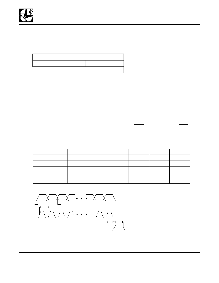
As show in Figure 2, after these 160 bits are clocked into the ICS309, taking STROBE high will send this
data to the internal latch and the CLK output will lock within 10 ms.
Note: STROBE utilizes a transparent latch that is latched when in the high state. If STROBE is in the high
state and SCLK is pulsed, DATA is clocked directly to the internal latch and the output conditions will
change accordingly. Although this will not damage the ICS309, it is recommended that STROBE be kept
low while DATA is being clocked into the ICS309 in order to avoid unintended changes on the output clocks.
All outputs may be turned off during initialization by bringing the PDTS pin to Ground. When PDTS is
brought high, after the Strobe pin in brought high, the programmed output frequencies will be available.
AC Parameters for Writing to the ICS309
Default Outputs
Output
Frequency
Clocks 1 - 9 (Pins 4, 7-14)
Reference Output
Parameter
Condition
Min. Max.
Units
t
SETUP
Setup time
10
ns
t
HOLD
Hold time after SCLK
10
ns
t
W
Data wait time
10
ns
t
S
Strobe pulse width
40
ns
SCLK Frequency
30
MHz
D ATA
t
hold
t
setup
S CLK
S TR O B E
t
s
t
w
Figure 2. Tim ing D iagram for Program m ing the IC S309
Bit160
Bit2
Bit1
Bit3
Bit159
Bit158

S
ERIAL
P
ROGRAMMABLE
T
RIPLE
PLL SS V
ERSA
C
LOCK
S
YNTHESIZER
MDS 309 G
4
Revision 122704
I n t e gr a t e d C i r c u i t S y s t e m s
5 2 5 R a c e S t r e e t , S a n J o s e, C A 9 5 1 2 6
t e l ( 4 0 8 ) 2 9 7 - 1 2 0 1
w w w. i c s t . c o m
ICS309
External Components
Series Termination Resistor
Clock output traces over one inch should use series
termination. To series terminate a 50
trace (a
commonly used trace impedance), place a 33
resistor
in series with the clock line, as close to the clock output
pin as possible. The nominal impedance of the clock
output is 20
.
STROBE Pull-up Resistor
In order for the device to start up in the default state, a
250 kOhm pull-up resistor is required.
Decoupling Capacitors
As with any high-performance mixed-signal IC, the
ICS309 must be isolated from system power supply
noise to perform optimally.
Decoupling capacitors of 0.01µF must be connected
between each VDD and the PCB ground plane.
Crystal Load Capacitors
The device crystal connections should include pads for
small capacitors from X1 to ground and from X2 to
ground. These capacitors are used to adjust the stray
capacitance of the board to match the nominally
required crystal load capacitance. Because load
capacitance can only be increased in this trimming
process, it is important to keep stray capacitance to a
minimum by using very short PCB traces (and no vias)
been the crystal and device. Crystal capacitors must be
connected from each of the pins X1 and X2 to ground.
The value (in pF) of these crystal caps should equal
(C
L
-6 pF)*2. In this equation, C
L
= crystal load
capacitance in pF. Example: For a crystal with a 16 pF
load capacitance, each crystal capacitor would be 20
pF [(16-6) x 2] = 20.
PCB Layout Recommendations
For optimum device performance and lowest output
phase noise, the following guidelines should be
observed.
1) Each 0.01µF decoupling capacitor should be
mounted on the component side of the board as close
to the VDD pin as possible. No vias should be used
between decoupling capacitor and VDD pin. The PCB
trace to VDD pin should be kept as short as possible,
as should the PCB trace to the ground via.
2) The external crystal should be mounted just next to
the device with short traces. The X1 and X2 traces
should not be routed next to each other with minimum
spaces, instead they should be separated and away
from other traces.
3) To minimize EMI, the 33
series termination resistor
(if needed) should be placed close to each clock
output.
4) An optimum layout is one with all components on the
same side of the board, minimizing vias through other
signal layers.
ICS309 Configuration Capabilities
The architecture of the ICS309 allows the user to easily
configure the device to a wide range of output
frequencies, for a given input reference frequency.
The frequency multiplier PLL provides a high degree of
precision. The M/N values (the multiplier/divide values
available to generate the target VCO frequency) can be
set within the range of M = 1 to 2048 and N = 1 to 1024.
The ICS309 also provides separate output divide
values, from 2 through 20, to allow the two output clock
banks to support widely differing frequency values from
the same PLL.
Each output frequency can be represented as:
Output Freq. = (Ref. Freq)*(M/N)/Output Divide
ICS VersaClock Software
ICS applies years of PLL optimization experience into a
user friendly software that accepts the user's target
reference clock and output frequencies and generates
the lowest jitter, lowest power configuration, with only a
press of a button. The user does not need to have prior
PLL experience or determine the optimal VCO
frequency to support multiple output frequencies.
VersaClock software quickly evaluates accessible VCO
frequencies with available output divide values and
provides an easy to understand, bar code rating for the
target output frequencies. The user may evaluate
output accuracy, performance trade-off scenarios in
seconds.
S
ERIAL
P
ROGRAMMABLE
T
RIPLE
PLL SS V
ERSA
C
LOCK
S
YNTHESIZER
MDS 309 G
5
Revision 122704
I n t e gr a t e d C i r c u i t S y s t e m s
5 2 5 R a c e S t r e e t , S a n J o s e, C A 9 5 1 2 6
t e l ( 4 0 8 ) 2 9 7 - 1 2 0 1
w w w. i c s t . c o m
ICS309
Spread Spectrum Modulation
The ICS309 utilizes frequency modulation (FM) to
distribute energy over a range of frequencies. By
modulating the output clock frequencies, the device
effectively lowers energy across a broader range of
frequencies; thus, lowering a system's
electro-magnetic interference (EMI). The modulation
rate is the time from transitioning from a minimum
frequency to a maximum frequency and then back to
the minimum.
Spread Spectrum Modulation can be applied as either
"center spread" or "down spread". During center spread
modulation, the deviation from the target frequency is
equal in the positive and negative directions. The
effective average frequency is equal to the target
frequency. In applications where the clock is driving a
component with a maximum frequency rating, down
spread should be applied. In this case, the maximum
frequency, including modulation, is the target
frequency. The effective average frequency is less than
the target frequency.
The ICS309 operates in both center spread and down
spread modes. For center spread, the frequency can
be modulated between ±0.125% to ±2.0%. For down
spread, the frequency can be modulated between
-0.25% to -4.0%.
Both output frequency banks will utilize identical spread
spectrum percentage deviations and modulation rates,
if a common VCO frequency can be identified.
Spread Spectrum Modulation Rate
The spread spectrum modulation frequency applied to
the output clock frequency may occur at a variety of
rates. For applications requiring the driving of
"down-circuit" PLLs, Zero Delay Buffers, or those
adhering to PCI standards, the spread spectrum
modulation rate should be set to 30-33 kHz. For other
applications, a 120 kHz modulation option is available.
Absolute Maximum Ratings
Stresses above the ratings listed below can cause permanent damage to the ICS309. These ratings, which
are standard values for ICS commercially rated parts, are stress ratings only. Functional operation of the
device at these or any other conditions above those indicated in the operational sections of the
specifications is not implied. Exposure to absolute maximum rating conditions for extended periods can
affect product reliability. Electrical parameters are guaranteed only over the recommended operating
temperature range.
Recommended Operation Conditions
Parameter
Condition
Min.
Typ.
Max.
Units
Supply Voltage, VDD
Referenced to GND
7
V
Inputs
Referenced to GND
-0.5
VDD+ 0.5
V
Clock Outputs
Referenced to GND
-0.5
VDD+ 0.5
V
Storage Temperature
-65
150
∞C
Soldering Temperature
Max 10 seconds
260
∞C
Parameter
Min.
Typ.
Max.
Units
Ambient Operating Temperature
0
+70
∞C
Ambient Operating Temperature (ICS309RI)
-40
+85
∞C
Power Supply Voltage (measured in respect to GND)
+3.0
+3.6
V
Power Supply Ramp Time
4
ms
S
ERIAL
P
ROGRAMMABLE
T
RIPLE
PLL SS V
ERSA
C
LOCK
S
YNTHESIZER
MDS 309 G
6
Revision 122704
I n t e gr a t e d C i r c u i t S y s t e m s
5 2 5 R a c e S t r e e t , S a n J o s e, C A 9 5 1 2 6
t e l ( 4 0 8 ) 2 9 7 - 1 2 0 1
w w w. i c s t . c o m
ICS309
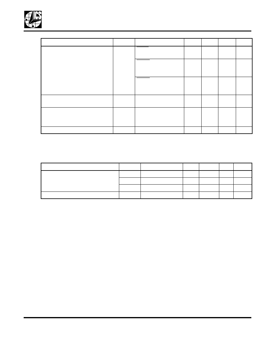
DC Electrical Characteristics
VDD=3.3 V ±10%
, Ambient temperature -40 to +85
∞C, unless stated otherwise
AC Electrical Characteristics
VDD = 3.3 V ±10%
, Ambient Temperature -40 to +85
∞ C, unless stated otherwise
Parameter
Symbol
Conditions
Min.
Typ.
Max.
Units
Operating Voltage
VDD
3.00
3.60
V
Operating Supply Current
Input High Voltage
IDD
Configuration
Dependent - See
VersaClock
TM
Estimates
mA
Ex. 25 MHz crystal,
VDD=3.3V, No load,
9 - 33.3333 MHz outs,
PDTS = 1
25
mA
PDTS = 0
20
µA
Input High Voltage
V
IH
X1/ICLK only
(VDD/2)+1
V
Input Low Voltage
V
IL
X1/ICLK only
(VDD/2)-1
V
Input High Voltage
V
IH
VDD-0.5
V
Input Low Voltage
V
IL
PDTS, SCLK, DATA,
STROBE
0.8
V
Output High Voltage
V
OH
I
OH
= -8 mA
2.4
V
Output Low Voltage
V
OL
I
OL
= 8 mA
0.4
V
Output High Voltage,
CMOS level
V
OH
I
OH
= -4 mA
VDD-0.4
V
Short Circuit Current
CLK outputs
+70
mA
Input Capacitance
C
IN
PDTS pin
4
pF
Internal pull-down resistor
R
PD
CLK outputs
525
k
Internal Pull-up Resistor
R
PU
PDTS pin
250
k
Parameter
Symbol
Conditions
Min.
Typ.
Max.
Units
Input Frequency
F
IN
Fundamental crystal
5
27
MHz
Input Clock
2
50
MHz
Output Frequency
VDD=3.3 V
0.25
200
MHz
Output Clock Rise Time
t
OR
20% to 80%, Note 1
0.8
ns
Output Clock Fall Time
t
OF
80% to 20%, Note 1
0.8
ns
Output Clock Duty Cycle
Note 2
40
49-51
60
%
S
ERIAL
P
ROGRAMMABLE
T
RIPLE
PLL SS V
ERSA
C
LOCK
S
YNTHESIZER
MDS 309 G
7
Revision 122704
I n t e gr a t e d C i r c u i t S y s t e m s
5 2 5 R a c e S t r e e t , S a n J o s e, C A 9 5 1 2 6
t e l ( 4 0 8 ) 2 9 7 - 1 2 0 1
w w w. i c s t . c o m
ICS309
Note 1: Measured with 15 pF load.
Note 2: Duty Cycle is configuration dependent. Most configurations are min 45% / max 55%
Thermal Characteristics
Power-up time
PDTS goes high until
stable CLK output
4
10
ms
PDTS goes high until
stable CLK out,
Spread Spectrum off
.2
2
ms
PDTS goes high until
stable CLK out,
Spread Spectrum On
4
7
ms
Maximum Output Jitter, short term
t
j
Reference Clock
±300
ps
Maximum Output Jitter, short term
t
j
All other clocks,
C
L
=15 pF
Configuration
±200
ps
Pin-to-Pin Skew
Low Skew Outputs
-250
250
ps
Parameter
Symbol
Conditions
Min.
Typ.
Max.
Units
Thermal Resistance Junction to
Ambient
JA
Still air
135
∞C/W
JA
1 m/s air flow
93
∞C/W
JA
3 m/s air flow
78
∞C/W
Thermal Resistance Junction to Case
JC
60
∞C/W
Parameter
Symbol
Conditions
Min.
Typ.
Max.
Units

S
ERIAL
P
ROGRAMMABLE
T
RIPLE
PLL SS V
ERSA
C
LOCK
S
YNTHESIZER
MDS 309 G
8
Revision 122704
I n t e gr a t e d C i r c u i t S y s t e m s
5 2 5 R a c e S t r e e t , S a n J o s e, C A 9 5 1 2 6
t e l ( 4 0 8 ) 2 9 7 - 1 2 0 1
w w w. i c s t . c o m
ICS309
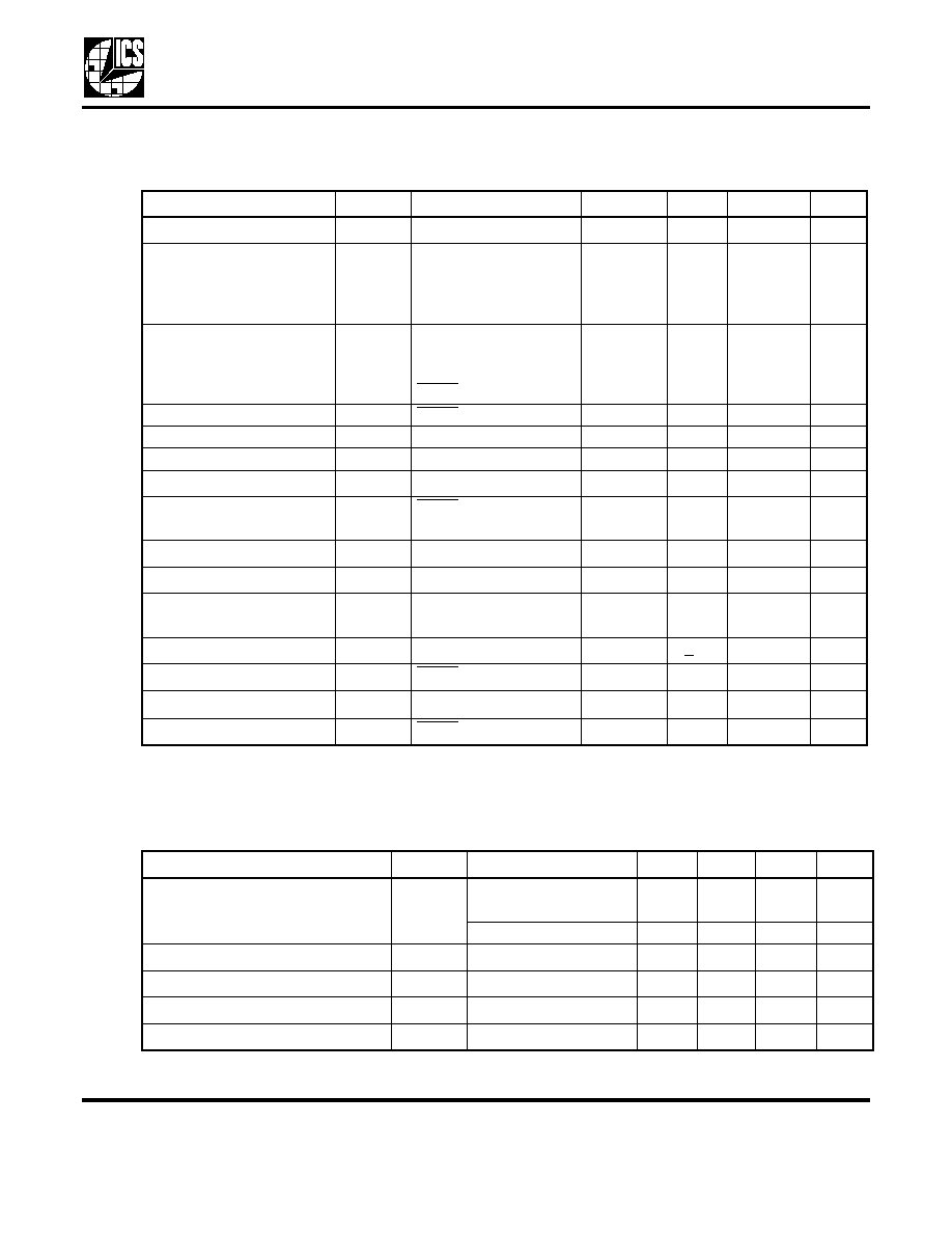
Package Outline and Package Dimensions
(20-pin SSOP, 150 Mil. Wide Body)
Package dimensions are kept current with JEDEC Publication No. 95
Ordering Information
While the information presented herein has been checked for both accuracy and reliability, Integrated Circuit Systems (ICS)
assumes no responsibility for either its use or for the infringement of any patents or other rights of third parties, which would
result from its use. No other circuits, patents, or licenses are implied. This product is intended for use in normal commercial
applications. Any other applications such as those requiring extended temperature range, high reliability, or other extraordinary
environmental requirements are not recommended without additional processing by ICS. ICS reserves the right to change any
circuitry or specifications without notice. ICS does not authorize or warrant any ICS product for use in life support devices or
critical medical instruments.
Part / Order Number
Marking
Shipping packaging
Package
Temperature
ICS309R
ICS309R (top line)
YYWW (2nd line)
Tubes
20-pin SSOP
0 to +70
∞ C
ICS309RT
Tape and Reel
20-pin SSOP
0 to +70
∞ C
ICS309RI
ICS309RI (top line)
YYWW (2nd line)
Tubes
20-pin SSOP
-40 to +85
∞ C
ICS309RIT
Tape and Reel
20-pin SSOP
-40 to +85
∞ C
INDEX
AREA
1 2
20
D
E1
E
SEATING
PLANE
A1
A
A2
e
- C -
b
aaa
C
c
L
Millimeters
Inches
Symbol
Min
Max
Min
Max
A
1.35
1.75
0.053
0.069
A1
0.10
0.25
0.004
0.010
A2
--
1.50
--
0.059
b
0.20
0.30
0.008
0.012
c
0.18
0.25
0.007
0.010
D
8.55
8.75
0.337
0.344
E
5.80
6.20
0.228
0.244
E1
3.80
4.00
0.150
0.157
e
.635 Basic
.025 Basic
L
0.40
1.27
0.016
0.050
0
∞
8
∞
0
∞
8
∞
aaa
--
0.10
--
0.004