 | –≠–ª–µ–∫—Ç—Ä–æ–Ω–Ω—ã–π –∫–æ–º–ø–æ–Ω–µ–Ω—Ç: ICS663MI | –°–∫–∞—á–∞—Ç—å:  PDF PDF  ZIP ZIP |
ICS663
MDS 663 D
1
Revision 062904
I n t e gra t e d C i r c u i t S y s t e m s
5 2 5 R a c e S t r e e t , S a n J o s e, C A 9 5 1 2 6
t e l ( 4 0 8 ) 2 9 7 - 1 2 0 1
w w w. i c s t . c o m
PLL B
UILDING
B
LOCK
Description
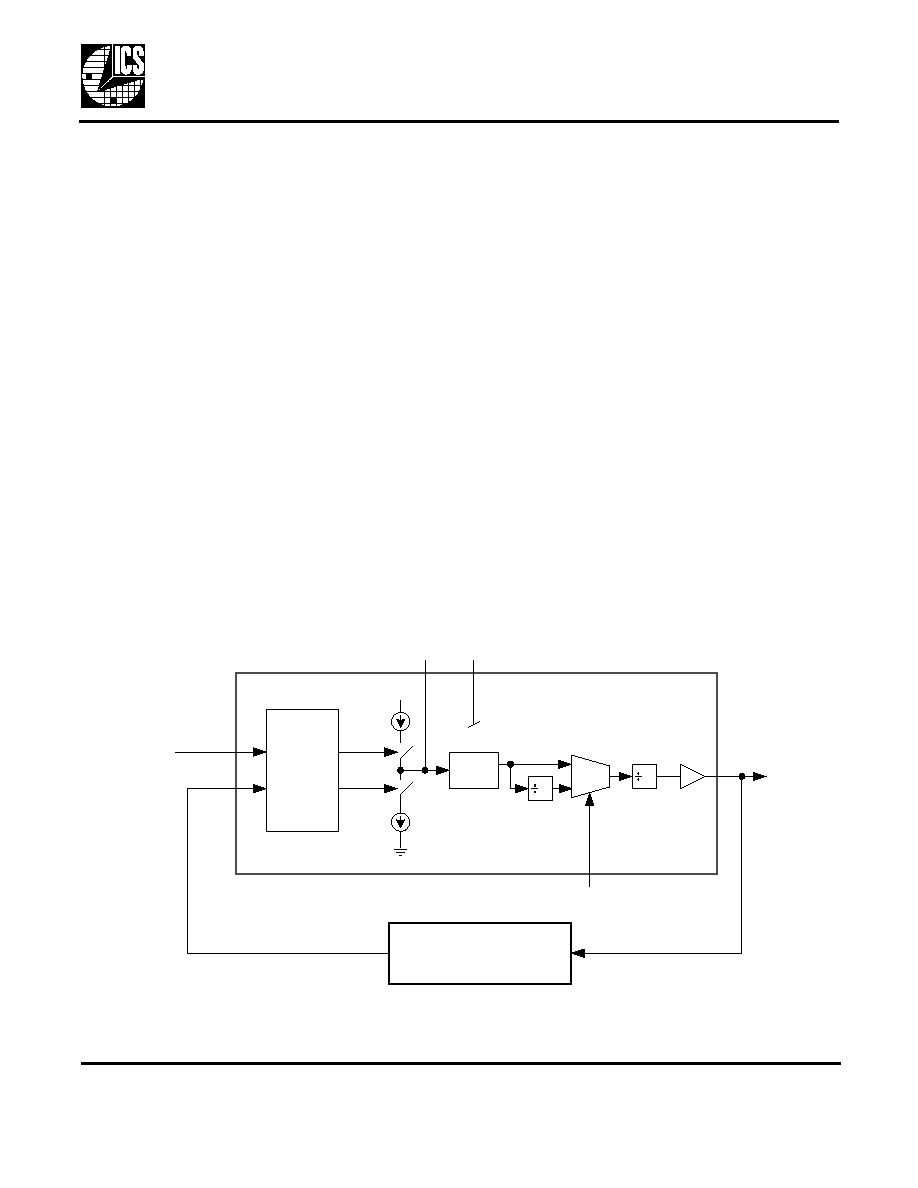
The ICS663 is a low cost Phase-Locked Loop (PLL)
designed for clock synthesis and synchronization.
Included on the chip are the phase detector, charge
pump, Voltage Controlled Oscillator (VCO) and an
output buffer. Through the use of external reference
and VCO dividers (implemented with the ICS674-01,
for example), the user can easily configure the device
to lock to a wide variety of input frequencies.
The phase detector and VCO functions of the device
can also be used independently. This enables the
configuration of other PLL circuits. For example, the
ICS663 phase detector can be used to control a VCXO
circuit such as the MK3754.
For applications requiring Power Down or Output
Enable features, please refer to the ICS673-01.
Features
∑
Packaged in 8-pin SOIC
∑
Output clock range 1 MHz to 100 MHz (3.3 V), 1 MHz
to 120 MHz (5 V)
∑
External PLL loop filter enables configuration for a
wide range of input frequencies
∑
Ability to accept an input clock in the kHz range
(video Hsync, for example)
∑
25 mA output drive capability at TTL levels
∑
Lower power CMOS process
∑
+3.3 V ±5% or +5 V ±10% operating voltage
∑
Used along with the ICS674-01, forms a complete
PLL circuit
∑
Phase detector and VCO blocks can be used
independently for other PLL configurations
∑
Industrial temperature version available
∑
For better jitter performance, use the MK1575
Block Diagram
R E F IN
P h a se /
F re qu e n cy
D e te cto r
V C O
4
2
S E L
L F R
LF
U P
F B IN
D O W N
I
cp
I
cp
C L K
V D D
M U X
1
0
E xternal F eedback D ivider
(such as the IC S 674-01)
C lock Input
PLL B
UILDING
B
LOCK
MDS 663 D
2
Revision 062904
I n t e gr a t e d C i r c u i t S y s t e m s
5 2 5 R a c e S t r e e t , S a n J o s e, C A 9 5 1 2 6
t e l ( 4 0 8 ) 2 9 7 - 1 2 0 1
w w w. i c s t . c o m
ICS663
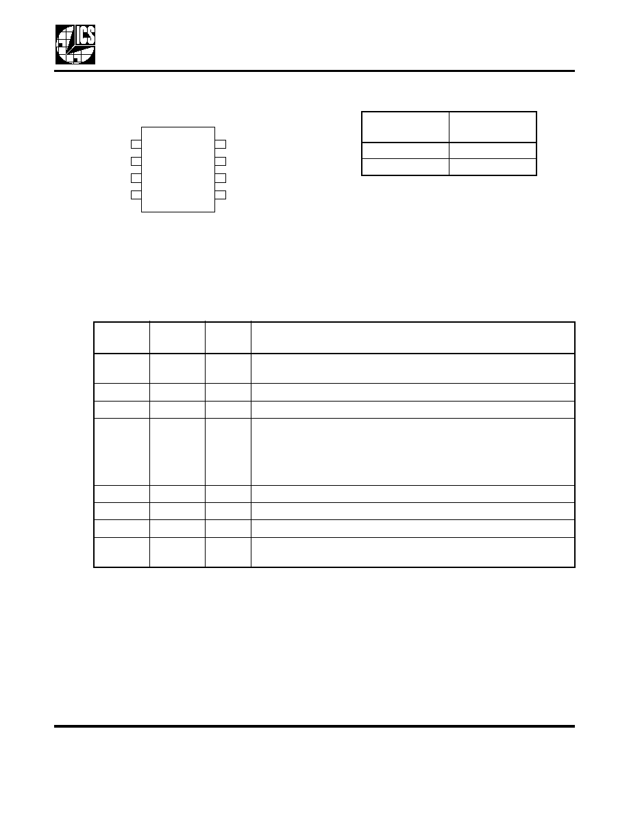
Pin Assignment
VCO Post Divide Select Table
0 = connect pin directly to ground
1 = connect pin directly to VDD
Pin Descriptions
1
2
3
FBIN
4
VDD
GND
CLK
LF
SEL
LFR
8
7
6
5
REFIN
8 Pin (150 mil) SOIC
SEL
VCO Post
Divide
0
8
1
2
Pin
Number
Pin
Name
Pin
Type
Pin Description
1
FBIN
Input
Feedback clock input. Connect the output of the feedback divider to
this pin. Falling edge triggered.
2
VDD
Power
VDD. Connect to +3.3 V or +5 V.
3
GND
Power
Connect to ground.
4
LF
Input
Loop filter connection (refer to Figure 1 on Page 5).
When using the phase detector block only, this pin serves as the
charge pump output.
When using the VCO block only, this pin serves as VCO input control
voltage.
5
LFR
Input
Loop filter return (refer to Figure 1 on Page 5).
6
SEL
Input
Select pin for VCO post divide, as per above table.
7
CLK
Output
Clock output.
8
REFIN
Input
Reference clock input. Connect the input clock to this pin. Falling edge
triggered.

PLL B
UILDING
B
LOCK
MDS 663 D
3
Revision 062904
I n t e gr a t e d C i r c u i t S y s t e m s
5 2 5 R a c e S t r e e t , S a n J o s e, C A 9 5 1 2 6
t e l ( 4 0 8 ) 2 9 7 - 1 2 0 1
w w w. i c s t . c o m
ICS663
Absolute Maximum Ratings
Stresses above the ratings listed below can cause permanent damage to the ICS663. These ratings, which
are standard values for ICS commercially rated parts, are stress ratings only. Functional operation of the
device at these or any other conditions above those indicated in the operational sections of the
specifications is not implied. Exposure to absolute maximum rating conditions for extended periods can
affect product reliability. Electrical parameters are guaranteed only over the recommended operating
temperature range.
Recommended Operation Conditions
DC Electrical Characteristics
VDD=3.3 V ±5% or 5.0 V ±10%, Ambient temperature -40 to +85
∞C, unless stated otherwise
Item
Rating
Supply Voltage, VDD
7V
All Inputs and Outputs
-0.5V to VDD+0.5V
Ambient Operating Temperature
0 to +70
∞C
Industrial Temperature
-40 to +85
∞C
Storage Temperature
-65 to +150
∞C
Soldering Temperature
260
∞C
Parameter
Min.
Typ.
Max.
Units
Ambient Operating Temperature
-40
+85
∞C
Power Supply Voltage (measured in respect to GND)
+3.13
+5.5
V
Parameter
Symbol
Conditions
Min.
Typ.
Max.
Units
Operating Voltage
VDD
3.13
5.5
V
Logic Input High Voltage
V
IH
REFIN, FBIN,
SEL
2
V
Logic Input Low Voltage
V
IL
REFIN, FBIN,
SEL
0.8
V
LF Input Voltage Range
V
I
0
VDD
V
Output High Voltage
V
OH
I
OH
= -25 mA
2.4
V
Output Low Voltage
V
OL
I
OL
= 25 mA
0.4
V
Output High Voltage, CMOS
level
V
OH
I
OH
= -8 mA
VDD-0.4
Operating Supply Current
IDD
VDD = 5.0 V,
No load, 40 MHz
15
mA
Short Circuit Current
I
OS
CLK
±100
mA
Input Capacitance
C
I
SEL
5
pF
PLL B
UILDING
B
LOCK
MDS 663 D
4
Revision 062904
I n t e gr a t e d C i r c u i t S y s t e m s
5 2 5 R a c e S t r e e t , S a n J o s e, C A 9 5 1 2 6
t e l ( 4 0 8 ) 2 9 7 - 1 2 0 1
w w w. i c s t . c o m
ICS663
AC Electrical Characteristics
VDD = 3.3 V ±5%, Ambient Temperature -40 to +85
∞ C, unless stated otherwise
VDD = 5.0 V ±10%, Ambient Temperature -40 to +85
∞ C, unless stated otherwise
Note 1: Minimum input frequency is limited by loop filter design. 1 kHz is a practical minimum limit.
Thermal Characteristics
Parameter
Symbol
Conditions
Min.
Typ.
Max.
Units
Output Clock Frequency
(from pin CLK)
f
CLK
SEL = 1
1
100
MHz
SEL = 0
0.25
25
MHz
Input Clock Frequency
(into pins REFIN or FBIN)
f
REF
Note 1
8
MHz
Output Rise Time
t
OR
0.8 to 2.0V
1.2
2
ns
Output Fall Time
t
OF
2.0 to 0.8V
0.75
1.5
ns
Output Clock Duty Cycle
t
DC
At VDD/2
40
50
60
%
Jitter, Absolute peak-to-peak
t
J
250
ps
VCO Gain
K
O
200
MHz/V
Charge Pump Current
I
cp
2.5
µA
Parameter
Symbol
Conditions
Min.
Typ.
Max.
Units
Output Clock Frequency
(from pin CLK)
f
CLK
SEL = 1
1
120
MHz
SEL = 0
0.25
30
MHz
Input Clock Frequency
(into pins REFIN or FBIN)
f
REF
Note 1
8
MHz
Output Rise Time
t
OR
0.8 to 2.0 V
0.5
1
ns
Output Fall Time
t
OF
2.0 to 0.8 V
0.5
1
ns
Output Clock Duty Cycle
t
DC
At VDD/2
45
50
55
%
Jitter, Absolute peak-to-peak
t
J
150
ps
VCO Gain
K
O
200
MHz/V
Charge Pump Current
I
cp
2.5
µA
Parameter
Symbol
Conditions
Min.
Typ.
Max.
Units
Thermal Resistance Junction to
Ambient
JA
Still air
150
∞C/W
JA
1 m/s air flow
140
∞C/W
JA
3 m/s air flow
120
∞C/W
Thermal Resistance Junction to Case
JC
40
∞C/W
PLL B
UILDING
B
LOCK
MDS 663 D
5
Revision 062904
I n t e gr a t e d C i r c u i t S y s t e m s
5 2 5 R a c e S t r e e t , S a n J o s e, C A 9 5 1 2 6
t e l ( 4 0 8 ) 2 9 7 - 1 2 0 1
w w w. i c s t . c o m
ICS663
External Components
The ICS663 requires a minimum number of external
components for proper operation. A decoupling
capacitor of 0.01
µF should be connected between VDD
and GND as close to the ICS663 as possible. A series
termination resistor of 33
may be used at the clock
output.
Special considerations must be made in choosing loop
components C
1
and C
2
:
1) The loop capacitors should be a low-leakage type to
avoid leakage-induced phase noise. For this reason,
DO NOT use any type of polarized or electrolytic
capacitors.
2) Microphonics (mechanical board vibration) can also
induce output phase noise when the loop bandwidth is
less than 1 kHz. For this reason, ceramic capacitors
should have C0G or NP0 dielectric. Avoid high-K
dielectrics like Z5U and X7R. These and some other
ceramics have piezoelectric properties that convert
mechanical vibration into voltage noise that interferes
with VCXO operation.
For larger loop capacitor values such as 0.1
µF or 1µF,
PPS film types made by Panasonic, or metal poly types
made by Murata or Cornell Dubilier are recommended.
For questions or changes regarding loop filter
characteristics, please contact your sales area FAE, or
ICS Applications.
Avoiding PLL Lockup
In some applications, the ICS663 can "lock up" at the
maximum VCO frequency. The way to avoid this
problem is to use an external divider that always
operates correctly regardless of the CLK output
frequency. The CLK output frequency may be up to 2x
the maximum Output Clock Frequency listed in the AC
Electrical Characteristics above when the device is in
an unlocked condition. Make sure that the external
divider can operate up to this frequency.
Explanation of Operation
The ICS663 is a PLL building block circuit that includes
an integrated VCO with a wide operating range. The
device uses external PLL loop filter components which
through proper configuration allow for low input clock
reference frequencies, such as a 15.7 kHz Hsync input.
The phase/frequency detector compares the falling
edges of the clocks inputted to FBIN and REFIN. It then
generates an error signal to the charge pump, which
produces a charge proportional to this error. The
external loop filter integrates this charge, producing a
voltage that then controls the frequency of the VCO.
This process continues until the edges of FBIN are
aligned with the edges of the REFIN clock, at which
point the output frequency will be locked to the input
frequency.
Figure 1. Example Configuration
-- Generating a 20 MHz clock from a 200 kHz reference
R E F IN
+ 3 .3 or 5 V
V D D
S E L
0.01µ F
F B IN
200 kH z
100
D igital D iv ider such as
IC S 674-01
G N D
C LK
LF R
20 M H z
LF
C
1
R
Z
C
2
200 kH z
IC S 6 6 3

PLL B
UILDING
B
LOCK
MDS 663 D
6
Revision 062904
I n t e gr a t e d C i r c u i t S y s t e m s
5 2 5 R a c e S t r e e t , S a n J o s e, C A 9 5 1 2 6
t e l ( 4 0 8 ) 2 9 7 - 1 2 0 1
w w w. i c s t . c o m
ICS663
Determining the Loop Filter Values
The loop filter components consist of C
1
, C
2
, and R
Z
.
Calculating these values is best illustrated by an
example. Using the example in Figure 1, we can
synthesize 20 MHz from a 200 kHz input.
The phase locked loop may be approximately
described by the following equations:
Bandwidth
Damping factor,
where:
K
O
= VCO gain (MHz/Volt)
I
cp
= Charge pump current (
µA)
N = Total feedback divide from VCO,
including the internal VCO post divider
C
1
= Loop filter capacitor (Farads)
R
Z
= Loop filter resistor (Ohms)
As a general rule, the bandwidth should be at least 20
times less than the reference frequency, i.e.,
In this example, using the above equation, bandwidth
should be less than or equal to 10 kHz. By setting the
bandwith to 10kHz and using the first equation, R
Z
can
be determined since all other variables are known. In
the example of Figure 1, N = 200, comprising the divide
by 2 on the chip (VCO post divider) and the external
divide by 100. Therefore, the bandwidth equation
becomes:
and R
Z
= 25 k
Choosing a damping factor of 0.7 (a minimal damping
factor than can be used to ensure fast lock time),
damping factor equation becomes:
and C
1
= 1.25 nF (1.2 nF is the nearest standard
value).
The capacitor C
2
is used to damp transients from the
charge pump and should be approximately 1/20th the
size of C
1
, i.e.,
Therefore, C
2
= 60 pF (56 pF nearest standard value).
To summarize, the loop filter components are:
C
1
= 1.2 nf
C
2
= 56 pf
R
z
= 25 k
R
Z
K
O
I
CP
(
)
2
N
------------------------------------
=
R
Z
2
------
K
O
I
CP
C
1
N
-------------------------------
=
BW
REFIN
(
) 20
/
10,000
R
Z
200 2.5
2
200
--------------------------------
=
0.7
25 000
,
2
------------------
200 2.5 C
1
200
---------------------------------
=
C
2
C
1
20
/

PLL B
UILDING
B
LOCK
MDS 663 D
7
Revision 062904
I n t e gr a t e d C i r c u i t S y s t e m s
5 2 5 R a c e S t r e e t , S a n J o s e, C A 9 5 1 2 6
t e l ( 4 0 8 ) 2 9 7 - 1 2 0 1
w w w. i c s t . c o m
ICS663
Package Outline and Package Dimensions
(8-pin SOIC, 150 Mil. Narrow Body)
Package dimensions are kept current with JEDEC Publication No. 95
Ordering Information
While the information presented herein has been checked for both accuracy and reliability, Integrated Circuit Systems (ICS)
assumes no responsibility for either its use or for the infringement of any patents or other rights of third parties, which would
result from its use. No other circuits, patents, or licenses are implied. This product is intended for use in normal commercial
applications. Any other applications such as those requiring extended temperature range, high reliability, or other extraordinary
environmental requirements are not recommended without additional processing by ICS. ICS reserves the right to change any
circuitry or specifications without notice. ICS does not authorize or warrant any ICS product for use in life support devices or
critical medical instruments.
Part / Order Number
Marking
Shipping Packaging
Package
Temperature
ICS663M
ICS663M
Tubes
8-pin SOIC
0 to +70
∞ C
ICS663MT
ICS663M
Tape and Reel
8-pin SOIC
0 to +70
∞ C
ICS663MI
ICS663MI
Tubes
8-pin SOIC
-40 to +85
∞ C
ICS663MIT
ICS663MI
Tape and Reel
8-pin SOIC
-40 to +85
∞ C
INDEX
AREA
1 2
8
D
E
SEATING
PLANE
A1
A
e
- C -
B
.10 (.004)
C
C
L
H
h x 45
Millimeters
Inches
Symbol
Min
Max
Min
Max
A
1.35
1.75
.0532
.0688
A1
0.10
0.25
.0040
.0098
B
0.33
0.51
.013
.020
C
0.19
0.25
.0075
.0098
D
4.80
5.00
.1890
.1968
E
3.80
4.00
.1497
.1574
e
1.27 BASIC
0.050 BASIC
H
5.80
6.20
.2284
.2440
h
0.25
0.50
.010
.020
L
0.40
1.27
.016
.050
0
∞
8
∞
0
∞
8
∞