 | –≠–ª–µ–∫—Ç—Ä–æ–Ω–Ω—ã–π –∫–æ–º–ø–æ–Ω–µ–Ω—Ç: ICS95V847 | –°–∫–∞—á–∞—Ç—å:  PDF PDF  ZIP ZIP |

Integrated
Circuit
Systems, Inc.
ICS95V847
0718D--04/08/05
Block Diagram
PLL
FB_INT
FB_INC
CLK_INC
CLK_INT
FB_OUTT
FB_OUTC
CLKT0
CLKT1
CLKT2
CLKT3
CLKT4
CLKC0
CLKC1
CLKC2
CLKC3
CLKC4
2.5V Wide Range Frequency Clock Driver (45MHz - 233MHz)
Pin Configuration
24-Pin TSSOP
Recommended Application:
∑
Zero Delay Board Fan Out, SO-DIMM
∑
Provides complete DDR registered DIMM solution
with ICSSSTV16857, ICSSSTV16859 or
ICSSSTV32852
Product Description/Features:
∑
Low skew, low jitter PLL clock driver
∑
1 to 5 differential clock distribution (SSTL_2)
∑
Feedback pins for input to output synchronization
∑
Spread Spectrum tolerant inputs
Switching Characteristics:
∑
CYCLE - CYCLE jitter: <60ps
∑
OUTPUT - OUTPUT skew: <60ps
∑
Period jitter: ±30ps
∑
DUTY CYCLE: 49.5% - 50.5%
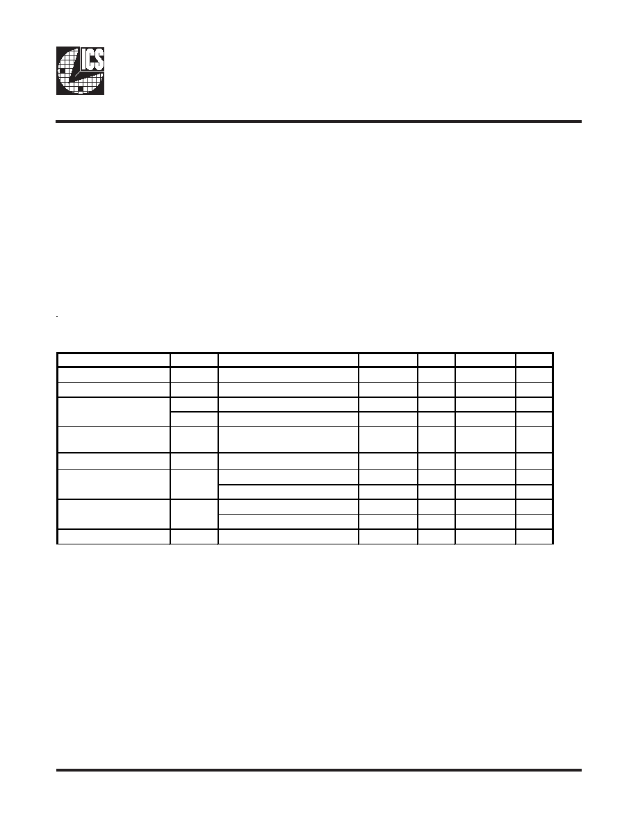
Functionality
S
T
U
P
N
I
S
T
U
P
T
U
O
e
t
a
t
S
L
L
P
D
D
V
A
T
N
I
_
K
L
C
C
N
I
_
K
L
C
T
K
L
C
C
K
L
C
T
T
U
O
_
B
F
C
T
U
O
_
B
F
D
N
G
L
H
L
H
L
H
f
f
o
/
d
e
s
s
a
p
y
B
D
N
G
H
L
H
L
H
L
f
f
o
/
d
e
s
s
a
p
y
B
V
5
.
2
)
m
o
n
(
L
H
L
H
L
H
n
o
V
5
.
2
)
m
o
n
(
H
L
H
L
H
L
n
o
4.40 mm. Body, 0.65 mm. pitch
GND
CLKC0
CLKT0
GND
VDD
CLK_INT
CLK_INC
AVDD
AGND
CLKC1
CLKT1
VDD
CLKT4
CLKC4
CLKC3
CLKT3
VDD
FB_INT
FB_INC
FB_OUTC
FB_OUTT
CLKT2
CLKC2
GND
ICS95V
8
47
1
2
3
4
5
6
7
8
9
10
11
12
24
23
22
21
20
19
18
17
16
15
14
13

2
ICS95V847
0718D--04/08/05
Pin Descriptions
This PLL Clock Buffer is designed for a V
DD
of 2.5V, an AV
DD
of 2.5V and differential data input and output levels.
ICS95V847 is a zero delay buffer that distributes a differential clock input pair (CLK_INT, CLK_INC) to five differential
pair of clock outputs (CLKT[4:0], CLKC[4:0]) and one differential pair feedback clock output (FB_OUT, FB_OUTC). The
clock outputs are controlled by input clock (CLK_INT, CLK_INC), the feedback clock (FB_INT, FB_INC) and the analog
power input (AV
DD
). When AV
DD
is grounded, the PLL is turned off and bypassed for test purposes.
The PLL in ICS95V847 clock driver uses the input clock (CLK_INC, CLK_INT) and the feedback clock (FB_INT,
FB_INC) to provide high-performance, low-skew, low-jitter differential output clocks (CLKT[4:0], CLKC[4:0]). ICS95V847
is also able to track Spread Spectrum Clock (SSC) for reduced EMI.
ICS95V847 is characterized for operation from 0∞C to 85∞C.
R
E
B
M
U
N
N
I
P
E
M
A
N
N
I
P
E
P
Y
T
N
O
I
T
P
I
R
C
S
E
D
0
2
,
2
1
,
5
D
D
V
R
W
P
V
5
.
2
,
y
l
p
p
u
s
r
e
w
o
P
3
1
,
4
,
1
D
N
G
R
W
P
d
n
u
o
r
G
8
D
D
V
A
R
W
P
V
5
.
2
,
y
l
p
p
u
s
r
e
w
o
p
g
o
l
a
n
A
9
D
N
G
A
R
W
P
d
n
u
o
r
g
g
o
l
a
n
A
4
2
,
1
2
,
5
1
,
1
1
,
3
]
4
:
0
[
T
K
L
C
T
U
O
s
t
u
p
t
u
o
r
i
a
p
l
a
i
t
n
e
r
e
f
f
i
d
f
o
k
c
o
l
C
"
e
u
r
T
"
3
2
,
2
2
,
4
1
,
0
1
,
2
]
4
:
0
[
C
K
L
C
T
U
O
s
t
u
p
t
u
o
r
i
a
p
l
a
i
t
n
e
r
e
f
f
i
d
f
o
s
k
c
o
l
c
"
y
r
a
t
n
e
m
e
l
p
m
o
C
"
6
T
N
I
_
K
L
C
N
I
t
u
p
n
i
k
c
o
l
c
e
c
n
e
r
e
f
e
r
"
e
u
r
T
"
7
C
N
I
_
K
L
C
N
I
t
u
p
n
i
k
c
o
l
c
e
c
n
e
r
e
f
e
r
"
y
r
a
t
n
e
m
e
l
p
m
o
C
"
6
1
T
T
U
O
_
B
F
T
U
O
s
e
h
c
t
i
w
s
t
I
.
k
c
a
b
d
e
e
f
l
a
n
r
e
t
x
e
r
o
f
d
e
t
a
c
i
d
e
d
,
t
u
p
t
u
o
k
c
a
b
d
e
e
F
"
"
e
u
r
T
"
o
t
d
e
r
i
w
e
b
t
s
u
m
t
u
p
t
u
o
s
i
h
T
.
K
L
C
e
h
t
s
a
y
c
n
e
u
q
e
r
f
e
m
a
s
e
h
t
t
a
T
N
I
_
B
F
7
1
C
T
U
O
_
B
F
T
U
O
t
I
.
k
c
a
b
d
e
e
f
l
a
n
r
e
t
x
e
r
o
f
d
e
t
a
c
i
d
e
d
,
t
u
p
t
u
o
k
c
a
b
d
e
e
F
"
y
r
a
t
n
e
m
e
l
p
m
o
C
"
d
e
r
i
w
e
b
t
s
u
m
t
u
p
t
u
o
s
i
h
T
.
K
L
C
e
h
t
s
a
y
c
n
e
u
q
e
r
f
e
m
a
s
e
h
t
t
a
s
e
h
c
t
i
w
s
C
N
I
_
B
F
o
t
9
1
T
N
I
_
B
F
N
I
r
o
f
L
L
P
l
a
n
r
e
t
n
i
e
h
t
o
t
l
a
n
g
i
s
k
c
a
b
d
e
e
f
s
e
d
i
v
o
r
p
,
t
u
p
n
i
k
c
a
b
d
e
e
F
"
e
u
r
T
"
r
o
r
r
e
e
s
a
h
p
e
t
a
n
i
m
il
e
o
t
T
N
I
_
K
L
C
h
t
i
w
n
o
i
t
a
z
i
n
o
r
h
c
n
y
s
8
1
C
N
I
_
B
F
N
I
L
L
P
l
a
n
r
e
t
n
i
e
h
t
o
t
l
a
n
g
i
s
s
e
d
i
v
o
r
p
,
t
u
p
n
i
k
c
a
b
d
e
e
F
"
y
r
a
t
n
e
m
e
l
p
m
o
C
"
r
o
r
r
e
e
s
a
h
p
e
t
a
n
i
m
il
e
o
t
C
N
I
_
K
L
C
h
t
i
w
n
o
i
t
a
z
i
n
o
r
h
c
n
y
s
r
o
f
3
ICS95V847
0718D--04/08/05
Absolute Maximum Ratings
Supply Voltage (VDD & AVDD) . . . . . . . . . . . -0.5V to 4.6V
Logic Inputs . . . . . . . . . . . . . . . . . . . . . . . . . GND - 0.5V to V
DD
+ 0.5V
Ambient Operating Temperature . . . . . . . . . . 0∞C to +85∞C
Storage Temperature . . . . . . . . . . . . . . . . . . . -65∞C to +150∞C
Stresses above those listed under
Absolute Maximum Ratings may cause permanent damage to the device. These
ratings are stress specifications only and functional operation of the device at these or any other conditions above those
listed in the operational sections of the specifications is not implied. Exposure to absolute maximum rating conditions
for extended periods may affect product reliability.
Electrical Characteristics - Input/Supply/Common Output Parameters
T
A
= 0 - 85∞C; Supply Voltage A
VDD
, V
DD
= 2.5 V +/- 0.2V (unless otherwise stated)
PARAMETER
SYMBOL
CONDITIONS
MIN
TYP
MAX
UNITS
Input High Current
I
IH
V
I
= V
DD
or GND
5
µA
Input Low Current
I
IL
V
I
= V
DD
or GND
5
µA
I
DD2.5
C
L
= 0pf @ 200MHz
148
mA
I
DDPD
C
L
= 0pf
100
µA
High Impedance
Output Current
I
OZ
V
DD
= 2.7V, Vout = V
DD
or
GND
±10
mA
Input Clamp Voltage
V
IK
V
DD
= 2.3V Iin = -18mA
-1.2
V
I
OH
= -1 mA
V
DD
- 0.1
V
I
OH
= -12 mA
1.7V
V
I
OL
=1 mA
0.1
V
I
OH
=12 mA
0.6
V
Input Capacitance
1
C
IN
V
I
= GND or V
DD
2.5
3.5
pF
1
Guaranteed by design at 233MHz, not 100% tested in production.
Operating Supply
Current
High-level output
voltage
V
OH
Low-level output voltage
V
OL
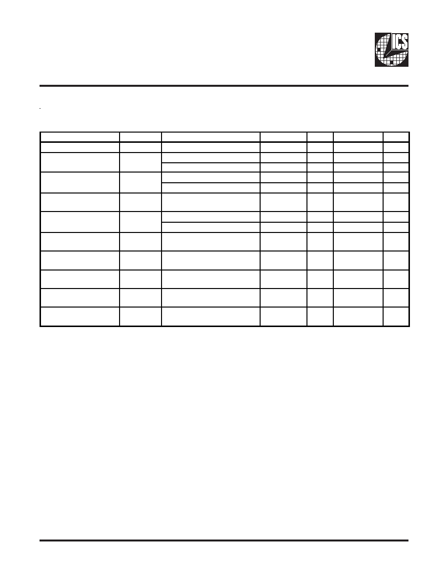
4
ICS95V847
0718D--04/08/05
Recommended Operating Condition (see note1)
T
A
= 0 - 85∞C; Supply Voltage AVDD, VDD = 2.5 V +/- 0.2V (unless otherwise stated)
PARAMETER
SYMBOL
CONDITIONS
MIN
TYP
MAX
UNITS
Supply Voltage
V
DD
, A
VDD
2.3
2.5
2.7
V
CLKT, CLKC, FB_INC
0.4
V
DD
/2 - 0.18
V
PD#
-0.3
0.7
V
CLKT, CLKC, FB_INC
V
DD
/2 + 0.18
2.1
V
PD#
1.7
V
DD
+ 0.6
V
DC input signal voltage
(note 2)
V
IN
-0.3
V
DD
+ 0.3
V
DC - CLKT, FB_INT
0.36
V
DD
+ 0.6
V
AC - CLKT, FB_INT
0.7
V
DD
+ 0.6
V
Output differential cross-
voltage (note 4)
V
OX
V
DD
/2 - 0.15
V
DD
/2 + 0.15
V
Input differential cross-
voltage (note 4)
V
IX
V
DD
/2 - 0.2
V
DD
/2
V
DD
/2 + 0.2
V
High level output
current
I
OH
-6.4
mA
Low level output current
I
OL
5.5
mA
Operating free-air
temperature
T
A
0
85
∞C
Differential input signal
voltage (note 3)
V
ID
Low level input voltage
V
IL
High level input voltage
V
IH
Notes:
1.
Unused inputs must be held high or low to prevent them from floating.
2.
DC input signal voltage specifies the allowable DC execution of differential input.
3.
Differential inputs signal voltages specifies the differential voltage [VTR-VCP]
required for switching, where VT is the true input level and VCP is the
complementary input level.
4.
Differential cross-point voltage is expected to track variations of V
DD
and is the
voltage at which the differential signal must be crossing.

5
ICS95V847
0718D--04/08/05
Notes:
1.
Refers to transition on noninverting output in PLL bypass mode.
2.
While the pulse skew is almost constant over frequency, the duty cycle error
increases at higher frequencies. This is due to the formula: duty cycle=t
wH
/t
c
, where
the cycle (t
c
) decreases as the frequency goes up.
3.
Switching characteristics guaranteed for application frequency range.
4.
Static phase offset shifted by design.
Timing Requirements
T
A
= 0 - 85∞C; Supply Voltage A
VDD
, V
DD
= 2.5 V +/- 0.2V (unless otherwise stated)
PARAMETER
SYMBOL
CONDITIONS
MIN
MAX
UNITS
Max clock frequency
freq
op
2.5V+0.2V @ 25
o
C
45
233
MHz
Application Frequency
Range
freq
App
2.5V+0.2V @ 25
o
C
95
210
MHz
Input clock duty cycle
d
tin
40
60
%
CLK stabilization
T
STAB
15
µs
Switching Characteristics (see note 3)
PARAMETER
SYMBOL
CONDITION
MIN
TYP
MAX
UNITS
Low-to high level
propagation delay time
t
PLH
1
CLK_IN to any output
5.5
ns
High-to low level propagation
delay time
t
PLL
1
CLK_IN to any output
5.5
ns
Output enable time
t
EN
PD# to any output
5
ns
Output disable time
tdis
PD# to any output
5
ns
Period jitter
T
jit (per)
100MHz to 200MHz
-30
30
ps
Half-period jitter
t(jit_hper)
100MHz to 200MHz
-75
30
ps
Input clock slew rate
t
sl(i)
1
4
V/ns
Output clock slew rate
t
sl(o)
1
2.5
V/ns
Cycle to Cycle Jitter
1
T
cyc
-T
cyc
100MHz to 200MHz
60
ps
Phase error
t
(phase error)
4
-50
0
50
ps
Output to Output Skew
T
skew
60
ps