Integrated Circuit Solution Inc.
1
LPSR018-0D 07/06/2001
IS62LV1024L/LL
ICSI reserves the right to make changes to its products at any time without notice in order to improve design and supply the best possible product. We assume no responsibility for any errors
which may appear in this publication. © Copyright 2000, Integrated Circuit Solution Inc.
DESCRIPTION
The
1+51
IS62LV1024L and IS62LV1024LL are low power
and low Vcc,131,072-word by 8-bit CMOS static RAMs. They
are fabricated using
1+51
's high-performance CMOS technol-
ogy. This highly reliable process coupled with innovative circuit
design techniques, yields higher performance and low power
consumption devices.
When CE1 is HIGH or CE2 is LOW (deselected), the device
assumes a standby mode at which the power dissipation can
be reduced by using CMOS input levels.
Easy memory expansion is provided by using two Chip Enable
inputs, CE1 and CE2. The active LOW Write Enable (WE)
controls both writing and reading of the memory.
The IS62LV1024L and IS62LV1024LL are available in 32-pin
8*20mm TSOP-1, 8*13.4mm TSOP-1, 450mil SOP and 48-pin
6*8mm T.-BGA.
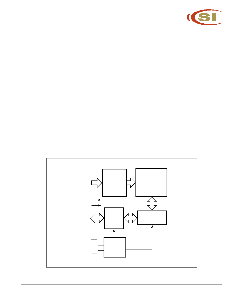
.UNCTIONAL BLOCK DIAGRAM
A0-A16
CE1
OE
WE
512 X 2048
MEMORY ARRAY
DECODER
COLUMN I/O
CONTROL
CIRCUIT
GND
VCC
I/O
DATA
CIRCUIT
I/O0-I/O7
CE2
IS62LV1024L
IS62LV1024LL
128K x 8 LOW POWER and LOW Vcc
CMOS STATIC RAM
.EATURES
Access times of 45, 55, and 70 ns
Low active power: 60 mW (typical)
Low standby power: 15 µW (typical) CMOS
standby
Low data retention voltage: 2V (min.)
Available in Low Power (-L) and
Ultra Low Power (-LL)
Output Enable (OE) and two Chip Enable
(CE1 and CE2) inputs for ease in applications
TTL compatible inputs and outputs
Single 2.7V to 3.6V power supply
2
Integrated Circuit Solution Inc.
LPSR018-0D 07/06/2001
IS62LV1024L/LL
1
2
3
4
5
6
7
8
9
10
11
12
13
14
15
16
32
31
30
29
28
27
26
25
24
23
22
21
20
19
18
17
NC
A16
A14
A12
A7
A6
A5
A4
A3
A2
A1
A0
I/O0
I/O1
I/O2
GND
VCC
A15
CE2
WE
A13
A8
A9
A11
OE
A10
CE1
I/O7
I/O6
I/O5
I/O4
I/O3
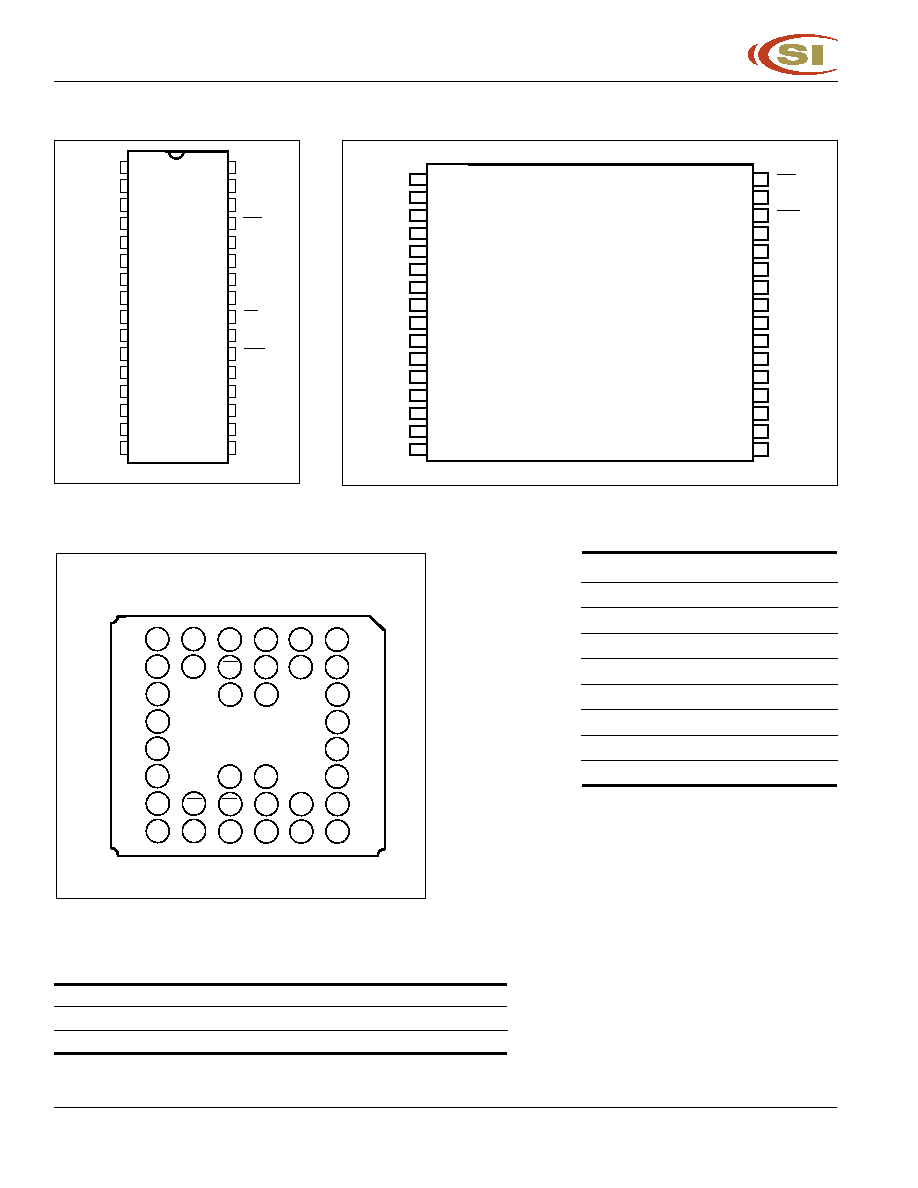
PIN CON.IGURATION
32-Pin SOP
PIN DESCRIPTIONS
A0-A16
Address Inputs
CE1
Chip Enable 1 Input
CE2
Chip Enable 2 Input
OE
Output Enable Input
WE
Write Enable Input
I/O0-I/O7
Input/Output
NCNo C
onnection
Vcc
Power
GND
Ground
1
2
3
4
5
6
7
8
9
10
11
12
13
14
15
16
32
31
30
29
28
27
26
25
24
23
22
21
20
19
18
17
A11
A9
A8
A13
WE
CE2
A15
VCC
NC
A16
A14
A12
A7
A6
A5
A4
OE
A10
CE1
I/O7
I/O6
I/O5
I/O4
I/O3
GND
I/O2
I/O1
I/O0
A0
A1
A2
A3
PIN CON.IGURATION
32-Pin 8x20mm TSOP-1 and 8x13.4mm TSOP-1
OPERATING RANGE
Range
Ambient Temperature
V
CC
Commercial
0∞C to +70∞C
2.7V to 3.6V
Industrial
40∞C to +85∞C
2.7V to 3.6V
48-Pin 6x8mm T.-BGA
1 2 3 4 5 6
A
B
C
D
E
F
G
H
A0
A1
CE2
A3
A6
A8
I/O
5
A2
WE
A4
A7
I/O
1
I/O
6
NC
A5
I/O
2
GND
Vcc
Vcc
GND
I/O
7
NC
NC
I/O
3
I/O
8
OE
CE1
A16
A15
I/O
4
A9
A10
A11
A12
A13
A14
Integrated Circuit Solution Inc.
3
LPSR018-0D 07/06/2001
IS62LV1024L/LL
ABSOLUTE MAXIMUM RATINGS
(1)
Symbol
Parameter
Value
Unit
V
TERM
Terminal Voltage with Respect to GND
0.5 to Vcc + 0.5
V
V
CC
Vcc related to GND
0.3 to +4.6
V
T
BIAS
Temperature Under Bias
40 to +85
∞C
T
STG
Storage Temperature
65 to +150
∞C
P
T
Power Dissipation
0.7
W
Notes:
1. Stress greater than those listed under ABSOLUTE MAXIMUM RATINGS may cause
permanent damage to the device. This is a stress rating only and functional operation of the
device at these or any other conditions above those indicated in the operational sections of
this specification is not implied. Exposure to absolute maximum rating conditions for
extended periods may affect reliability.
CAPACITANCE
(1,2)
Symbol
Parameter
Conditions
Max.
Unit
C
IN
Input Capacitance
V
IN
= 0V
6
p.
C
OUT
Output Capacitance
V
OUT
= 0V
8
p.
Notes:
1. Tested initially and after any design or process changes that may affect these parameters.
2. Test conditions: T
A
= 25∞C, f = 1 MHz, Vcc = 3.0V.
DC ELECTRICAL CHARACTERISTICS
(Over Operating Range)
Symbol Parameter
Test Conditions
Min.
Max.
Unit
V
OH
Output HIGH Voltage
V
CC
= Min., I
OH
= 1.0 mA
2.2
V
V
OL
Output LOW Voltage
V
CC
= Min., I
OL
= 2.1 mA
0.4
V
V
IH
Input HIGH Voltage
2.2
V
CC
+ 0.3
V
V
IL
Input LOW Voltage
0.3
0.4
V
I
LI
Input Leakage
GND
V
IN
V
CC
1
1
µA
I
LO
Output Leakage
GND
V
OUT
V
CC
1
1
µA
Notes:
1. V
IL
= 3.0V for pulse width less than 10 ns.
TRUTH TABLE
Mode
WE
WE
WE
WE
WE
CE1
CE1
CE1
CE1
CE1 CE2 OE
OE
OE
OE
OE
I/O Operation
Vcc Current
Not Selected
X
H
X
X
High-Z
I
SB
, I
SB
(Power-down)
X
X
L
X
High-Z
I
SB
, I
SB
Output Disabled H
L
H
H
High-Z
I
CC
Read
H
L
H
L
D
OUT
I
CC
Write
L
L
H
X
D
IN
I
CC
4
Integrated Circuit Solution Inc.
LPSR018-0D 07/06/2001
IS62LV1024L/LL
IS62LV1024L POWER SUPPLY CHARACTERISTICS
(1)
(Over Operating Range)
-45L ns
-55L ns
-70L ns
Symbol Parameter
Test Conditions
Min. Max.
Min. Max.
Min. Max.
Unit
I
CC
Vcc Dynamic Operating V
CC
= Max., CE = V
IL
Com.
40
35
30
mA
Supply Current
I
OUT
= 0 mA, f = f
MAX
Ind.
45
40
35
I
SB
TTL Standby Current
V
CC
= Max.,
Com.
0.3
0.3
0.3
mA
(TTL Inputs)
V
IN
= V
IH
or V
IL
, CE1
V
IH
Ind.
0.4
0.4
0.4
or CE2
V
IL
, f = 0
I
SB
CMOS Standby
V
CC
= Max., f = 0
Com.
50
50
50
µA
Current (CMOS Inputs)
CE1
V
CC
0.2V,
Ind.
75
75
75
CE2
0.2V,
or V
IN
V
CC
0.2V, V
IN
0.2V
Note:
1. At f = f
MAX
, address and data inputs are cycling at the maximum frequency, f = 0 means no input lines change.
IS62LV1024LL POWER SUPPLY CHARACTERISTICS
(1)
(Over Operating Range)
-45LL ns
-55LL ns
-70LL ns
Symbol Parameter
Test Conditions
Min. Max.
Min. Max.
Min. Max.
Unit
I
CC
Vcc Dynamic Operating V
CC
= Max., CE = V
IL
Com.
40
35
30
mA
Supply Current
I
OUT
= 0 mA, f = f
MAX
Ind.
45
40
35
I
SB
TTL Standby Current
V
CC
= Max.,
Com.
0.2
0.2
0.2
mA
(TTL Inputs)
V
IN
= V
IH
or V
IL
, CE1
V
IH
Ind.
0.3
0.3
0.3
or CE2
V
IL
, f = 0
I
SB
CMOS Standby
V
CC
= Max., f = 0
Com.
5
5
5
µA
Current (CMOS Inputs)
CE1
V
CC
0.2V,
Ind.
10
10
10
CE2
0.2V,
or V
IN
V
CC
0.2V, V
IN
0.2V
Note:
1. At f = f
MAX
, address and data inputs are cycling at the maximum frequency, f = 0 means no input lines change.
Integrated Circuit Solution Inc.
5
LPSR018-0D 07/06/2001
IS62LV1024L/LL
READ CYCLE SWITCHING CHARACTERISTICS
(1)
(Over Operating Range)
-45
-55
-70
Symbol Parameter
Min. Max.
Min. Max.
Min. Max.
Unit
t
RC
Read Cycle Time
45
55
70
ns
t
AA
Address Access Time
45
55
70
ns
t
OHA
Output Hold Time
10
10
10
ns
t
ACE
CE1 Access Time
45
55
70
ns
t
ACE
CE2 Access Time
45
55
70
ns
t
DOE
OE Access Time
20
25
35
ns
t
LZOE
OE to Low-Z Output
0
5
5
ns
t
HZOE
OE to High-Z Output
0
15
0
20
0
25
ns
t
LZCE
CE1 to Low-Z Output
5
7
10
ns
t
LZCE
CE2 to Low-Z Output
5
7
10
ns
t
HZCE
CE1 or CE2 to High-Z Output
0
15
0
20
0
25
ns
Notes:
1. Test conditions assume signal transition times of 5 ns or less, timing reference levels of 1.5V, input pulse levels of 0.4V to 2.2V
and output loading specified in .igure 1.
2. Tested with the load in .igure 2. Transition is measured ±500 mV from steady-state voltage. Not 100% tested.
AC TEST CONDITIONS
Parameter
Unit
Input Pulse Level
0.4V to 2.2V
Input Rise and .all Times
5 ns
Input and Output Timing
1.5V
and Reference Level
Output Load
See .igures 1
AC TEST LOADS
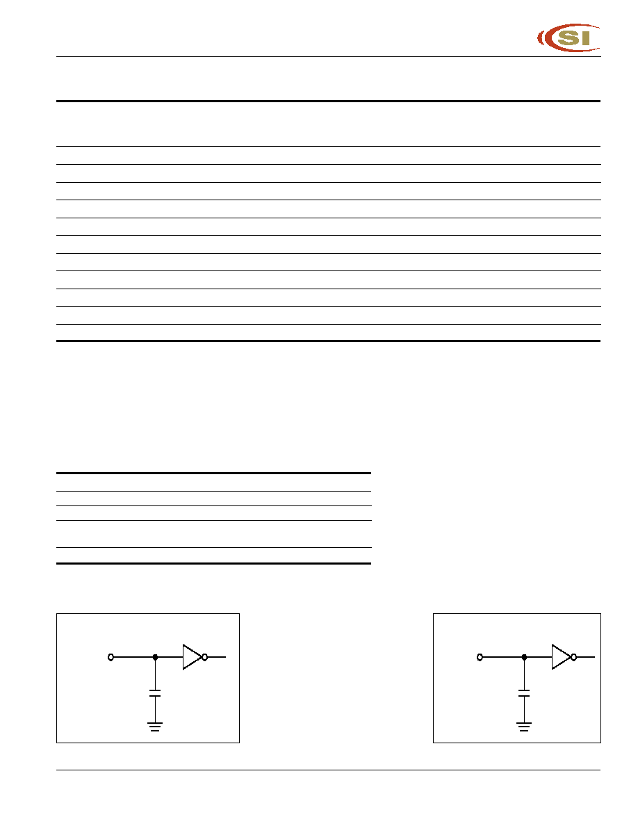
.igure 1.
.igure 2.
100 pF
Including
jig and
scope
OUTPUT
1 TTL
5 pF
Including
jig and
scope
OUTPUT
1 TTL