Integrated Circuit Solution Inc.
1
MC003-0B
IS80C54
IS80C58
ICSI reserves the right to make changes to its products at any time without notice in order to improve design and supply the best possible product. We assume no responsibility for any errors
which may appear in this publication. © Copyright 2000, Integrated Circuit Solution Inc.
IS80C54
IS80C58
CMOS SINGLE CHIP
8-BIT MICROCONTROLLER
FEATURES
·
80C52 based architecture
·
16K x 8 ROM (80C54)
32K x 8 ROM (80C58)
·
256 x 8 RAM
·
Three 16-bit Timer/Counters
·
Full duplex serial channel
·
Boolean processor
·
Four 8-bit I/O ports, 32 I/O lines
·
Memory addressing capability
64K ROM and 64K RAM
·
Program memory lock
Lock bits (2)
·
Power save modes:
Idle and power-down
·
Eight interrupt sources
·
Most instructions execute in 0.3 µs
·
CMOS and TTL compatible
·
Maximum speed: 40 MHz @ Vcc = 5V
·
Packages available:
40-pin DIP
44-pin PLCC
44-pin PQFP
GENERAL DESCRIPTION
The
ICSI
IS80C54 and IS80C58 are high-performance
microcontroller fabricated using high-density CMOS
technology. The CMOS IS80C54/58 is functionally
c o m p a t i b l e w i t h t h e i n d u s t r y s t a n d a r d 8 0 C 5 2 / 3 2
microcontrollers.
The IS80C54/58 is designed with 16K x 8 ROM (IS80C54
) a n d 3 2 K x 8 R O M ( I S 8 0 C 5 8 ) ; 2 5 6 x 8 R A M ; 3 2
programmable I/O lines; a serial I/O port for either
multiprocessor communications, I/O expansion or full duplex
UART; three 16-bit timer/counters; an eight-source, two-
priority-level, nested interrupt structure; and an on-chip
oscillator and clock circuit. The IS80C54/58 can be
expanded using standard TTL compatible memory.
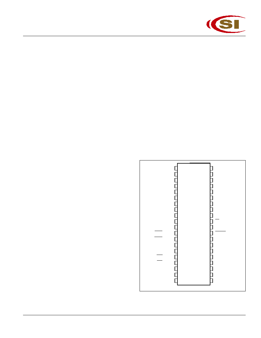
Figure 1. IS80C54/58 Pin Configuration: 40-pin DIP
1
2
3
4
5
6
7
8
9
10
11
12
13
14
15
16
17
18
19
20
40
39
38
37
36
35
34
33
32
31
30
29
28
27
26
25
24
23
22
21
T2/P1.0
T2EX/P1.1
P1.2
P1.3
P1.4
P1.5
P1.6
P1.7
RST
RxD/P3.0
TxD/P3.1
INT0/P3.2
INT1/P3.3
T0/P3.4
T1/P3.5
WR/P3.6
RD/P3.7
XTAL2
XTAL1
GND
V
CC
P0.0/AD0
P0.1/AD1
P0.2/AD2
P0.3/AD3
P0.4/AD4
P0.5/AD5
P0.6/AD6
P0.7/AD7
EA
ALE
PSEN
P2.7/A15
P2.6/A14
P2.5/A13
P2.4/A12
P2.3/A11
P2.2/A10
P2.1/A9
P2.0/A8

Integrated Circuit Solution Inc.
5
MC003-0B
IS80C54
IS80C58
Table 1. Detailed Pin Description
Symbol
PDIP
PLCC
PQFP
I/O
Name and Function
ALE
30
33
27
I/O
Address Latch Enable: Output pulse for latching the low byte
of the address during an access to the external memory. In
normal operation, ALE is emitted at a constant rate of 1/6 the
oscillator frequency, and can be used for external timing or
clocking. Note that one ALE pulse is skipped during each
access to external data memory.
EA
31
35
29
I
External Access enable:
EA must be externally held low to
enable the device to fetch code from external program memory
locations 0000H to FFFFH. If
EA is held high, the device
executes from internal program memory unless the program
counter contains an address greater than internal ROM seze.
P0.0-P0.7
39-32
43-36
37-30
I/O
Port 0: Port 0 is an 8-bit open-drain, bidirectional I/O port. Port
0 pins that have 1s written to them float and can be used as high-
impedance inputs. Port 0 is also the multiplexed low-order
address and data bus during accesses to external program and
data memory. In this application, it uses strong internal pullups
when emitting 1s.
P1.0-P1.7
1-8
2-9
40-44
I/O
Port 1: Port 1 is an 8-bit bidirectional I/O port with internal
1-3
pullups. Port 1 pins that have 1s written to them are pulled high
by the internal pullups and can be used as inputs. As inputs, Port
1 pins that are externally pulled low will source current because
of the internal pullups. (See DC Characteristics: I
IL
). The Port 1
output buffers can sink/source four TTL inputs.
Port 1 also receives the low-order address byte during verification.
1
2
40
I
T2(P1.0): Timer/Counter 2 external count input.
2
3
41
I
T2EX(P1.1): Timer/Counter 2 trigger input.
P2.0-P2.7
21-28
24-31
18-25
I/O
Port 2: Port 2 is an 8-bit bidirectional I/O port with internal
pullups. Port 2 pins that have 1s written to them are pulled high
by the internal pullups and can be used as inputs. As inputs, Port
2 pins that are externally pulled low will source current because
of the internal pullups. (See DC Characteristics: I
IL
). Port 2 emits
the high order address byte during fetches from external pro-
gram memory and during accesses to external data memory
that used 16-bit addresses (MOVX @ DPTR). In this application,
Port 2
uses strong internal pullups when emitting 1s. During
accesses to external data memory that use 8-bit addresses
(MOVX @ Ri [i = 0, 1]), Port 2 emits the contents of the P2
Special Function Register.
Port 2 also receives the high-order bits and some control signals
during verification.