 | –≠–ª–µ–∫—Ç—Ä–æ–Ω–Ω—ã–π –∫–æ–º–ø–æ–Ω–µ–Ω—Ç: V385GLFT | –°–∫–∞—á–∞—Ç—å:  PDF PDF  ZIP ZIP |
V385
V385 Datasheet
1
3/30/05
Revision 1.6
Integrated Circuit Systems ∑ 525 Race Street, San Jose, CA 95126 ∑ tel (408) 297-1201 ∑ www.icst.com
8-B
IT
LVDS T
RANSMITTER
FOR
V
IDEO
General Description
The V385 transmitter converts 28 bits of 3.3 V
CMOS/TTL into 4 Low Voltage Differential Signaling
(LVDS) data streams while the transmit clock input is
transmitted in parallel with the data streams over a fifth
LVDS link. The V385 can be programmed for rising
edge or falling edge clocks through pin R_FB.
ICS manufactures a large variety of video application
devices. Consult ICS for all of your video application
requirements.
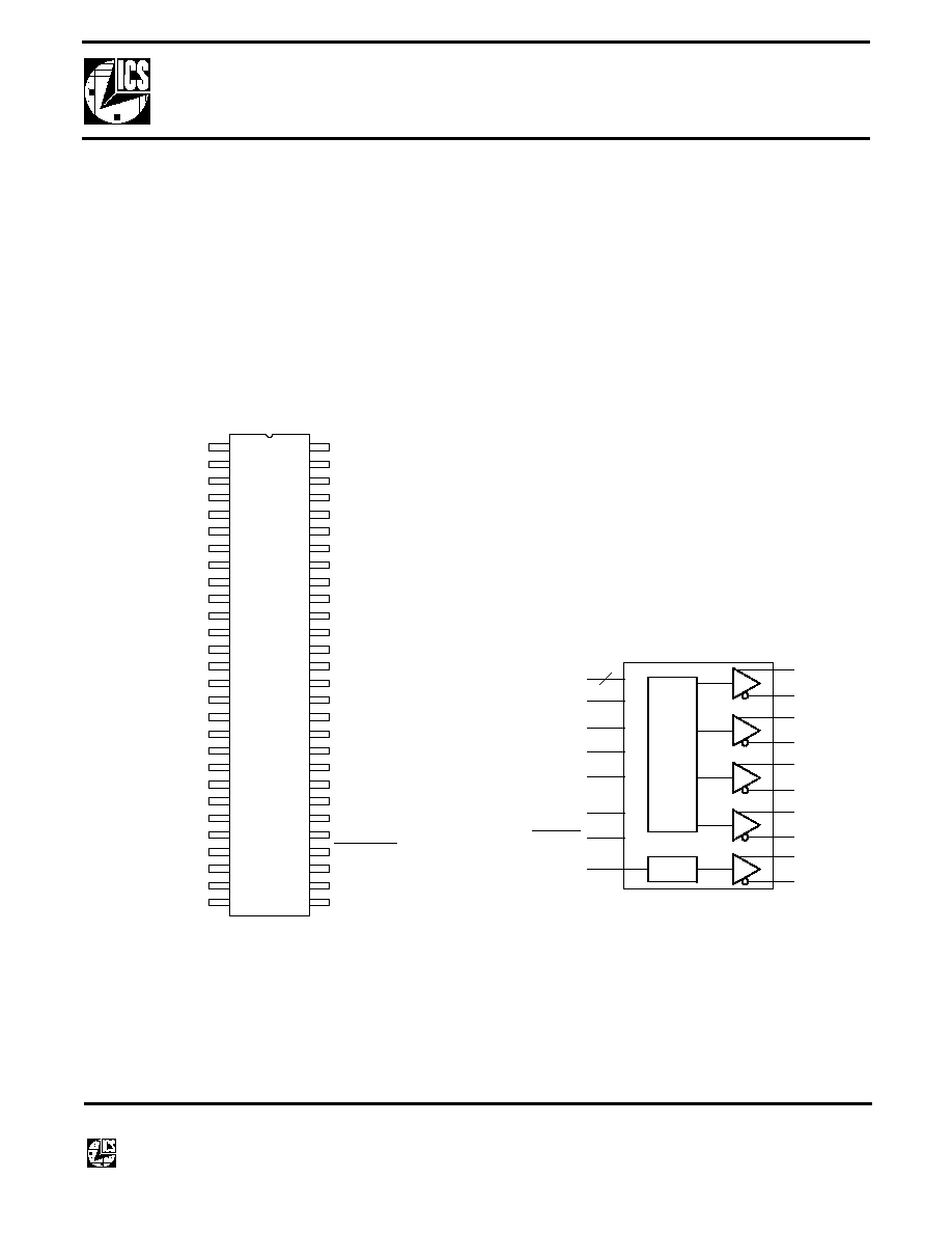
Pin Assignment
Features
∑
Pin and function compatible with the National
DS90C385, TI SN65LVDS93 and THine
THC63LVDM83
∑
Convert 28 bits of 3.3 V CMOS/TTL into 4 LVDS
streams
∑
Up to 2.38 Gbps throughput or 297.5 Megabytes/sec
bandwidth
∑
Wide clock frequency range from 20 MHz to 85 MHz
∑
Spread spectrum compatible
∑
Supports VGA, SVGA, XGA, and SXGA
∑
LVDS voltage swing of 350 mV for low EMI
∑
On-chip PLL requires no external components
∑
Single 3.3 V low-power CMOS design
∑
Programmable rising or falling edge strobe
∑
Power-down control function
∑
Compatible with TIA/EIA-644 LVDS standards
∑
Packaged in a 56-pin TSSOP (Pb free available)
Block Diagram
12
1
11
2
10
VCC
3
9
TxIN5
4
5
6
7
8
16
15
14
13
56-pin TSSOP
17
18
19
20
21
22
23
24
25
26
27
28
29
30
31
32
33
34
35
36
37
38
39
40
41
42
43
44
45
46
47
48
49
50
51
52
53
54
55
56
TxIN6
TxIN7
TxIN8
TxIN9
TxIN10
GND
VCC
TxIN11
TxIN12
TxIN13
GND
TxIN14
TxIN15
TxIN16
R_FB
TxIN17
TxIN18
TxIN19
GND
TxIN20
TxIN21
TxIN22
TxIN23
TxIN24
TxIN25
VCC
GND
TxIN26
PWRDWN
PLL_GND
PLL_GND
PLL_VCC
LVDS_GND
LVDS_GND
LVDS_GND
LVDS_VCC
TxOUT3+
TxOUT3-
TxCLKOUT+
TxCLKOUT-
TxOUT2+
TxOUT2-
TxCLKIN
TxOUT1+
TxOUT1-
TxOUT0+
TxOUT0-
TxIN27
TxIN0
TxIN1
GND
TxIN2
TxIN3
TxIN4
TTL to
LVDS
TxOUT0+
PLL
TxOUT0-
TxOUT1+
TxOUT1-
TxOUT2+
TxOUT2-
TxOUT3+
TxOUT3-
TxCLKOUT+
TxCLKOUT-
24
Red, Green, Blue
CLOCK
PWRDWN
R_FB
CONTROL
DATA ENABLE
VSYNC
HSYNC
8-B
IT
LVDS T
RANSMITTER
FOR
V
IDEO
V385
V385 Datasheet
2
3/30/05
Revision 1.6
Integrated Circuit Systems ∑ 525 Race Street, San Jose, CA 95126 ∑ tel (408) 297-1201 ∑ www.icst.com
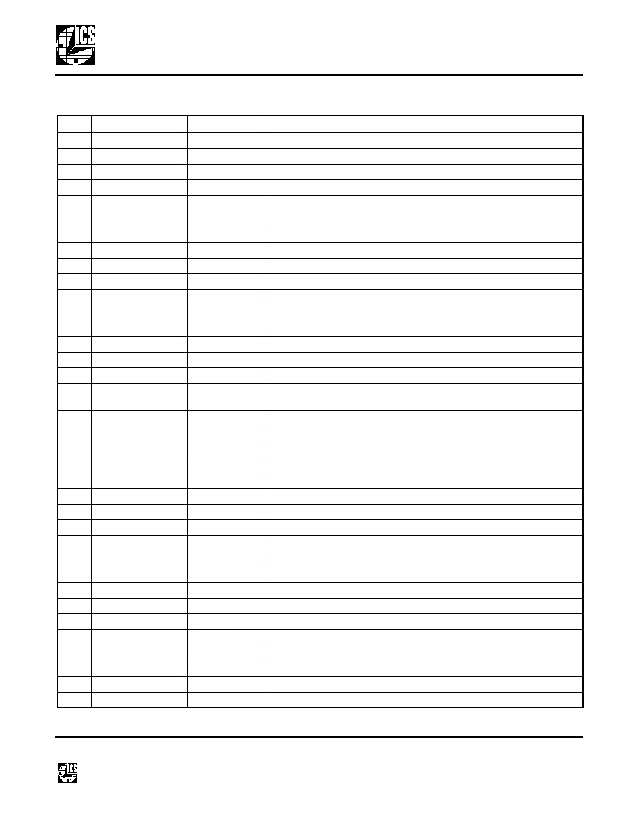
Pin Descriptions
Pin
Pin Type
Pin Name
Pin Description/Name
1
Power
VCC
3.3V Power
2
CMOS/TTL
TxIN5
Parallel digital video input pins (TxIN0..27).
3
CMOS/TTL
TxIn6
Parallel digital video input pins (TxIN0..27).
4
CMOS/TTL
TxIn7
Parallel digital video input pins (TxIN0..27).
5
Ground
GND
Ground
6
CMOS/TTL
TxIN8
Parallel digital video input pins (TxIN0..27).
7
CMOS/TTL
TxIN9
Parallel digital video input pins (TxIN0..27).
8
CMOS/TTL
TxIN10
Parallel digital video input pins (TxIN0..27).
9
Power
VCC
3.3V Power
10
CMOS/TTL
TxIN11
Parallel digital video input pins (TxIN0..27).
11
CMOS/TTL
TxIN12
Parallel digital video input pins (TxIN0..27).
12
CMOS/TTL
TxIN13
Parallel digital video input pins (TxIN0..27).
13
Ground
GND
Ground
14
CMOS/TTL
TxIN14
Parallel digital video input pins (TxIN0..27).
15
CMOS/TTL
TxIN15
Parallel digital video input pins (TxIN0..27).
16
CMOS/TTL
TxIN16
Parallel digital video input pins (TxIN0..27).
17
CMOS/TTL
R_FB
Programmable strobe select input pin (R_FB). High = rising edge; Low =
falling edge.
18
CMOS/TTL
TxIN17
Parallel digital video input pins (TxIN0..27).
19
CMOS/TTL
TxIN18
Parallel digital video input pins (TxIN0..27).
20
CMOS/TTL
TxIN19
Parallel digital video input pins (TxIN0..27).
21
Ground
GND
Ground
22
CMOS/TTL
TxIN20
Parallel digital video input pins (TxIN0..27).
23
CMOS/TTL
TxIN21
Parallel digital video input pins (TxIN0..27).
24
CMOS/TTL
TxIN22
Parallel digital video input pins (TxIN0..27).
25
CMOS/TTL
TxIN23
Parallel digital video input pins (TxIN0..27).
26
Power
VCC
3.3V Power
27
CMOS/TTL
TxIN24
Parallel digital video input pins (TxIN0..27).
28
CMOS/TTL
TxIN25
Parallel digital video input pins (TxIN0..27).
29
Ground
GND
Ground
30
CMOS/TTL
TxIN26
Parallel digital video input pins (TxIN0..27).
31
CMOS/TTL
TxCLKIN
Clock input (TxCLKIN)
32
CMOS/TTL
PWRDWN
Active low. Powerdown tri-states outputs.
33
Ground
PLL_GND
Ground
34
Power
PLL_VCC
3.3V Power
35
Ground
PLL_GND
Ground
36
Ground
LVDS_GND
Ground
8-B
IT
LVDS T
RANSMITTER
FOR
V
IDEO
V385
V385 Datasheet
3
3/30/05
Revision 1.6
Integrated Circuit Systems ∑ 525 Race Street, San Jose, CA 95126 ∑ tel (408) 297-1201 ∑ www.icst.com
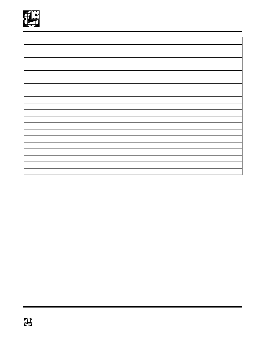
External Components
The V385 requires no external components.
37
LVDS
TxOUT3+
LVDS output (+)
38
LVDS
TxOUT3-
LVDS output (-)
39
LVDS
TxCLKOUT+
LVDS output (+)
40
LVDS
TxCLKOUT-
LVDS output (-)
41
LVDS
TxOUT2+
LVDS output (+)
42
LVDS
TxOUT2-
LVDS output (-)
43
Ground
LVDS_GND
Ground
44
Power
LVDS_VCC
3.3V Power
45
LVDS
TxOUT1+
LVDS output (+)
46
LVDS
TxOUT1-
LVDS output (-)
47
LVDS
TxOUT0+
LVDS output (+)
48
LVDS
TxOUT0-
LVDS output (-)
49
Ground
LVDS_GND
Ground
50
CMOS/TTL
TxIN27
Parallel digital video input pins (TxIN0..27).
51
CMOS/TTL
TxIn0
Parallel digital video input pins (TxIN0..27).
52
CMOS/TTL
TxIn1
Parallel digital video input pins (TxIN0..27).
53
Ground
GND
Ground
54
CMOS/TTL
TxIn2
Parallel digital video input pins (TxIN0..27).
55
CMOS/TTL
TxIn3
Parallel digital video input pins (TxIN0..27).
56
CMOS/TTL
TxIn4
Parallel digital video input pins (TxIN0..27).
Pin
Pin Type
Pin Name
Pin Description/Name

8-B
IT
LVDS T
RANSMITTER
FOR
V
IDEO
V385
V385 Datasheet
4
3/30/05
Revision 1.6
Integrated Circuit Systems ∑ 525 Race Street, San Jose, CA 95126 ∑ tel (408) 297-1201 ∑ www.icst.com
Absolute Maximum Ratings
Stresses above the ratings listed below can cause permanent damage to the V385. These ratings, which are
standard values for ICS commercially rated parts, are stress ratings only. Functional operation of the device at
these or any other conditions above those indicated in the operational sections of the specifications is not implied.
Exposure to absolute maximum rating conditions for extended periods can affect product reliability. Electrical
parameters are guaranteed only over the recommended operating temperature range.
Recommended Operation Conditions
Electrical Characteristics
VDD=3.3 V ±10%,
Ambient temperature 0 to +70
∞
C
Item
Rating
Supply Voltage, VDD
-0.3 V to +4 V
All Inputs and Outputs
-0.3 V to VCC+0.3 V
Electrostatic Discharge (EIAJ, 0
, 200 pF)
> 500 V
Ambient Operating Temperature
0 to +70
∞
C
Storage Temperature
-65 to +150
∞
C
Junction Temperature
150
∞
C
Maximum Soldering Temperature
260
∞
C
Parameter
Min.
Typ.
Max.
Units
Ambient Operating Temperature
0
+70
∞
C
Power Supply Voltage (measured in respect to GND)
3.0
3.3
3.6
V
Parameter
Symbol
Conditions
Min.
Typ.
Max.
Units
Freq.
CMOS/TTL DC Specifications
Input High Voltage
V
IH
2.00
VCC
V
Input Low Voltage
V
IL
GND
0.80
V
Input Current
I
IN
GND<VIN<VCC
±10
µ
A
Power-down Current
I
PD
No switching for input pins
10
µ
A
LVDS DC Specifications
Differential Output Voltage
V
OD
R
L
= 100 ohms
250
345
450
mV
Change in V
OD
Between
Complimentary Output States
V
OD
35
mV
Common Mode Voltage
V
CM
1.125
1.250
1.375
V
Change in V
CM
Between
Complimentary Output States
V
CM
35
mV
Output Short Circuit Current
I
OS
V
OD
=0V
3.5
5
mA
Output Tri-State Current
I
OZ
Power Down#=0V
±1
±10
µ
A

8-B
IT
LVDS T
RANSMITTER
FOR
V
IDEO
V385
V385 Datasheet
5
3/30/05
Revision 1.6
Integrated Circuit Systems ∑ 525 Race Street, San Jose, CA 95126 ∑ tel (408) 297-1201 ∑ www.icst.com
Thermal Characteristics
Recommended Transmitter Input Characteristics
TxCLK IN Transition Time
TCIT
5
ns
TxCLK IN Period
TCIP
11.76
T
50
ns
TxCLK IN High Time
TCIH
0.35T
0.5T
0.65T
ns
TxCLK IN Low Time
TCIL
0.35T
0.5T
0.65T
ns
TxIN Transition Time
TXIT
1.5
6
ns
Transmitter Switching Characteristics
LVDS Low-to-High Time
LLHT
0.75
1.4
ns
LVDS High-to-Low Time
LHLT
0.75
1.4
ns
Transmitter Output Pulse
Position
TPPos0
Bit0
-0.2
0
0.2
0.2
85 MHz
TPPos1
Bit1
T/7-0.2
T/7
T/7+0.2
ns
85 MHz
TPPos2
Bit2
2T/7-0.2
2T/7
2T/7+0.2
ns
85 MHz
TPPos3
Bit3
3T/7-0.2
3T/7
3T/7+0.2
ns
85 MHz
TPPos4
Bit4
4T/7-0.2
4T/7
4T/7+0.2
ns
85 MHz
TPPos5
Bit5
5T/7-0.2
5T/7
5T/7+0.2
ns
85 MHz
TPPos6
Bit6
6T/7-0.2
6T/7
6T/7+0.2
ns
85 MHz
Transmitter Phase Loop Set
TPLLS
10
ms
TxIN Setup to TxCLK IN
TSTC
2.5
ns
TxIN Hold to TxCLK IN
THTC
0
ns
TxCLK IN to TxCLK OUT
Delay
TCCD
10
30
ns
Parameter
Symbol
Conditions
Min.
Typ.
Max.
Units
Thermal Resistance Junction to Ambient
JA
Still air
84
∞
C/W
JA
1 m/s air flow
76
∞
C/W
JA
3 m/s air flow
67
∞
C/W
Thermal Resistance Junction to Case
JC
50
∞
C/W
Parameter
Symbol
Conditions
Min.
Typ.
Max.
Units
Freq.