
ICS511
MDS 511 E
1
Revision 101102
I n t e g r a t e d C i r c u i t S y s t e m s
q
5 2 5 R a c e S t r e e t , S a n J o s e , CA 9 5 1 2 6
q
t e l ( 4 0 8 ) 2 9 5 - 9 8 0 0
q
w w w. ic s t . c o m
LOCO
TM
PLL C
LOCK
M
ULTIPLIER
Description
The ICS511 LOCO
TM
is the most cost effective way to
generate a high quality, high frequency clock output
from a lower frequency crystal or clock input. The name
LOCO stands for Low Cost Oscillator, as it is designed
to replace crystal oscillators in most electronic
systems. Using Phase-Locked-Loop (PLL) techniques,
the device uses a standard fundamental mode,
inexpensive crystal to produce output clocks up to 200
MHz.
Stored in the chip's ROM is the ability to generate nine
different multiplication factors, allowing one chip to
output many common frequencies (see table on page
2).
The device also has an output enable pin which
tri-states the clock output when the OE pin is taken low.
This product is intended for clock generation. It has low
output jitter (variation in the output period), but input to
output skew and jitter are not defined nor guaranteed.
For applications which require defined input to output
skew, use the ICS570B.
Features
�
Packaged as 8 pin SOIC or die
�
Upgrade of popular ICS501 with:
- changed multiplier table
- faster operating frequencies
- output duty cycle at VDD/2
�
Zero ppm multiplication error
�
Input crystal frequency of 5 - 27 MHz
�
Input clock frequency of 2 - 50 MHz
�
Output clock frequencies up to 200 MHz
�
Extremely low jitter of 25 ps (one sigma)
�
Compatible with all popular CPUs
�
Duty cycle of 45/55 up to 200 MHz
�
Mask option for nine selectable frequencies
�
Operating voltage of 3.3V or 5V
�
Tri-state output for board level testing
�
Industrial temperature version available
�
Advanced, low power CMOS process
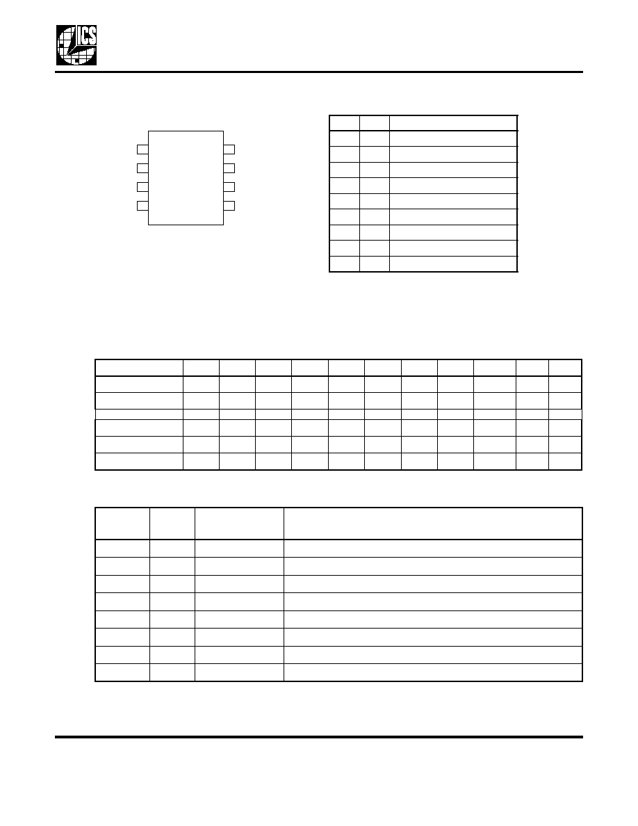
Block Diagram
CLK
PLL Clock
M ultiplier
Circuitry
and ROM
Crystal or
Clock input
GND
OE
VDD
Crystal
O scillator
S1:0
X1/ICLK
X2
O ptional crystal capacitors
2
LOCO
TM
PLL Clock Multiplier
MDS 511 E
2
Revision 101102
I n t e g r a t e d C i r c u i t S y s t e m s
q
5 2 5 Ra c e S t r e e t , S a n J o s e , C A 9 5 1 2 6
q
t e l ( 4 0 8 ) 2 9 5 - 9 8 0 0
q
w w w. i c s t . c o m
ICS511
Pin Assignment
Clock Output Table
0 = connect directly to ground
1 = connect directly to VDD
M = leave unconnected (floating)
Common Output Frequency Examples (MHz)
Pin Descriptions
X1/ I CLK
VDD
GND
OE
S1
S0
CLK
X2
1
2
3
4
8
7
6
5
8 Pi n ( 150 mi l ) SOI C
S1
S0
CLK
0
0
4X input
0
M
5.333X input
0
1
5X input
M
0
2.5X input
M
M
2X input
M
1
3.333X input
1
0
6X input
1
M
3X input
1
1
8X input
Output
20
24
30
32
33.33
37.5
40
48
50
60
64
Input
10
12
10
16
16.66
15
10
12
20
10
16
Selection (S1, S0)
M, M
M, M
1, M
M, M
M, M
M, 0
0, 0
0, 0
M, 0
1, 0
0, 0
Output
66.66
72
75
80
83.33
90
100
120
125
133.3
150
Input
20
12
25
10
25
15
20
15
25
25
25
Selection (S1, S0)
M, 1
1, 0
1, M
1, 1
M, 1
1, 0
0, 1
1, 1
0, 1
0, M
1, 0
Pin
Number
Pin
Name
Pin
Type
Pin Description
1
XI/ICLK
Input
Crystal connection or clock input.
2
VDD
Power
Connect to +3.3V or +5V.
3
GND
Power
Connect to ground.
4
S1
Tri-level Iinput
Select 1 for output clock. Connect to GND or VDD or float.
5
CLK
Output
Clock output per table above.
6
S0
Tri-level Input
Select 0 for output clock. Connect to GND or VDD or float.
7
OE
Input
Output enable. Tri-states CLK output when low. Internal pull-up.
8
X2
Output
Crystal connection. Leave unconnected for clock input.
LOCO
TM
PLL Clock Multiplier
MDS 511 E
3
Revision 101102
I n t e g r a t e d C i r c u i t S y s t e m s
q
5 2 5 Ra c e S t r e e t , S a n J o s e , C A 9 5 1 2 6
q
t e l ( 4 0 8 ) 2 9 5 - 9 8 0 0
q
w w w. i c s t . c o m
ICS511
External Components
Decoupling Capacitor
As with any high performance mixed-signal IC, the
ICS511 must be isolated from system power supply
noise to perform optimally.
A decoupling capacitor of 0.01�F must be connected
between VDD and the GND. It must be connected
close to the ICS501 to minimize lead inductance. No
external power supply filtering is required for the
ICS501.
Series Termination Resistor
A 33
terminating resistor can be used next to the CLK
pin for trace lengths over one inch.
Crystal Load Capacitors
The total on-chip capacitance is approximately 12 pF. A
parallel resonant, fundamental mode crystal should be
used. The device crystal connections should include
pads for small capacitors from X1 to ground and from
X2 to ground. These capacitors are used to adjust the
stray capacitance of the board to match the nominally
required crystal load capacitance. Because load
capacitance can only be increased in this trimming
process, it is important to keep stray capacitance to a
minimum by using very short PCB traces (and no vias)
between the crystal and device. Crystal capacitors, if
needed, must be connected from each of the pins X1
and X2 to ground.
The value (in pF) of these crystal caps should equal
(C
L
-12pF)*2. In this equation, C
L
= crystal load
capacitance in pF. Example: For a crystal with a 16 pF
load capacitance, each crystal capacitor would be 8 pF
[(16-12) x 2] = 8.
Absolute Maximum Ratings
Stresses above the ratings listed below can cause permanent damage to the ICS511. These ratings, which
are standard values for ICS commercially rated parts, are stress ratings only. Functional operation of the
device at these or any other conditions above those indicated in the operational sections of the
specifications is not implied. Exposure to absolute maximum rating conditions for extended periods can
affect product reliability. Electrical parameters are guaranteed only over the recommended operating
temperature range.
Recommended Operation Conditions
Item
Rating
Supply Voltage, VDD
7V
All Inputs and Outputs
-0.5V to VDD+0.5V
Ambient Operating Temperature
-40 to +85
�
C
Storage Temperature
-65 to +150
�
C
Soldering Temperature
260
�
C
Parameter
Min.
Typ.
Max.
Units
Ambient Operating Temperature
0
+70
�
C
Power Supply Voltage (measured in respect to GND)
+3.0
+5.5
V
LOCO
TM
PLL Clock Multiplier
MDS 511 E
4
Revision 101102
I n t e g r a t e d C i r c u i t S y s t e m s
q
5 2 5 Ra c e S t r e e t , S a n J o s e , C A 9 5 1 2 6
q
t e l ( 4 0 8 ) 2 9 5 - 9 8 0 0
q
w w w. i c s t . c o m
ICS511
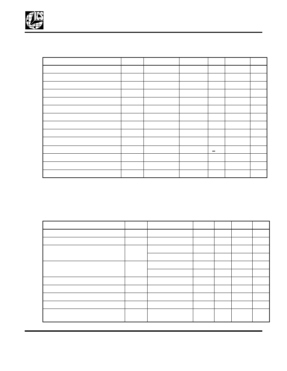
DC Electrical Characteristics
VDD=5.0V �5%
, Ambient temperature 0 to +70
�
C, unless stated otherwise
AC Electrical Characteristics
VDD = 5.0V �5%
, Ambient Temperature 0 to +70
�
C, unless stated otherwise
Parameter
Symbol
Conditions
Min.
Typ.
Max.
Units
Operating Voltage
VDD
3.0
5.5
V
Input High Voltage, ICLK only
V
IH
ICLK (pin 1)
(VDD/2)+1
V
Input Low Voltage, ICLK only
V
IL
ICLK (pin 1)
(VDD/2)-1
V
Input High Voltage
V
IH
OE (pin 7)
2.0
V
Input Low Voltage
V
IL
OE (pin 7)
0.8
V
Input High Voltage
V
IH
S0, S1
VDD-0.5
V
Input Low Voltage
V
IL
S0, S1
0.5
V
Output High Voltage
V
OH
I
OH
= -25 mA
2.4
V
Output Low Voltage
V
OL
I
OL
= 25 mA
0.4
V
IDD Operating Supply Current, 20
No load, 100M
9
mA
Short Circuit Current
CLK output
+70
mA
On-Chip Pull-up Resistor
Pin 7
270
k
Input Capacitance, S1, S0, and OE
Pins 4, 6, 7
4
pF
Nominal Output Impedance
20
Parameter
Symbol
Conditions
Min.
Typ.
Max.
Units
Input Frequency, crystal input
F
IN
5
27
MHz
Input Frequency, clock input
F
IN
2
50
MHz
Output Frequency, VDD = 4.5 to 5.5V
F
OUT
0
�
C to +70
�
C
14
200
MHz
-40
�
C to +85
�
C
14
160
MHz
Output Frequency, VDD = 3.0 to 3.6V
F
OUT
0
�
C to +70
�
C
14
160
MHz
-40
�
C to +85
�
C
14
145
MHz
Output Clock Rise Time
t
OR
0.8 to 2.0 V, Note 1
1
ns
Output Clock Fall Time
t
OF
2.0 to 8.0 V, Note 1
1
ns
Output Clock Duty Cycle
t
OD
1.5V, up to 160 MHz
45
49-51
55
%
PLL Bandwidth
10
kHz
Output Enable Time, OE high to
output on
50
ns

LOCO
TM
PLL Clock Multiplier
MDS 511 E
5
Revision 101102
I n t e g r a t e d C i r c u i t S y s t e m s
q
5 2 5 Ra c e S t r e e t , S a n J o s e , C A 9 5 1 2 6
q
t e l ( 4 0 8 ) 2 9 5 - 9 8 0 0
q
w w w. i c s t . c o m
ICS511
Note 1: Measured with 15 pF load.
Output Disable Time, OE low to
tri-state
50
ns
Absolute Clock Period Jitter
t
ja
Deviation from mean
+70
ps
One Sigma Clock Period Jitter
t
js
25
ps
Parameter
Symbol
Conditions
Min.
Typ.
Max.
Units