Document Outline
- General Description
- Features
- Block Diagram
- Pin Assignment
- Pin Descriptions
- Pin Characteristics
- Absolute Maximum Ratings
- Power Supply DC Characteristics
- LVCMOS DC Characteristics
- HSTL DC Characteristics
- 3.3V AC Characteristics
- 2.5V AC Characteristics
- Parameter Measurement Information
- Application Information
- Wiring the Differential Input to Accept Single Ended Levels
- Recommendations for Unused Input and Output Pins
- Schematic Example
- Power Considerations
- Power Dissipation
- Junction Temperature
- Thermal Resistance
- Calculations & Equations
- HSTL Driver Circuit & Termination Diagram
- Reliability Information
- Transistor Count
- Package Outline
- Package Dimensions
- Ordering Information
- Revision History Sheet
85222AM-01
www.icst.com/products/hiperclocks.html
REV. A NOVEMBER 15, 2005
1
Integrated
Circuit
Systems, Inc.
ICS85222-01
D
UAL
LVCMOS / LVTTL-
TO
-
D
IFFERENTIAL
HSTL T
RANSLATOR
G
ENERAL
D
ESCRIPTION
The ICS85222-01 is a Dual LVCMOS / LVTTL-
to-Differential HSTL translator and a member of
the HiPerClocksTM family of High Performance
Clock Solutions from ICS. The ICS85222-01 has
two single ended clock inputs. The single ended
clock input accepts LVCMOS or LVTTL input levels and trans-
lates them to HSTL levels. The small outline 8-pin SOIC pack-
age makes this device ideal for applications where space,
high performance and low power are important.
F
EATURES
� Two differential HSTL outputs
� CLK0, CLK1 LVCMOS/LVTTL clock inputs
� CLK0 and CLK1 can accept the following input levels:
LVCMOS or LVTTL
� Maximum output frequency: 350MHz
� Part-to-part skew: 375ps (maximum)
� Propagation delay: 1075ps (maximum)
� V
OH
: 1.4V (maximum)
� Full 3.3V and 2.5V operating supply voltage
� 0�C to 70�C ambient operating temperature
� Industrial temperature information available upon request
� Available in both standard and lead-free RoHS-compliant
packages
B
LOCK
D
IAGRAM
P
IN
A
SSIGNMENT
ICS85222-01
8-Lead SOIC
3.90mm x 4.92mm x 1.37mm body package
M Package
Top View
Q0
nQ0
Q1
nQ1
1
2
3
4
Q0
nQ0
Q1
nQ1
CLK0
CLK1
HiPerClockSTM
ICS
V
DD
CLK0
CLK1
GND
8
7
6
5
85222AM-01
www.icst.com/products/hiperclocks.html
REV. A NOVEMBER 15, 2005
2
Integrated
Circuit
Systems, Inc.
ICS85222-01
D
UAL
LVCMOS / LVTTL-
TO
-
D
IFFERENTIAL
HSTL T
RANSLATOR
T
ABLE
1. P
IN
D
ESCRIPTIONS
T
ABLE
2. P
IN
C
HARACTERISTICS
r
e
b
m
u
N
e
m
a
N
e
p
y
T
n
o
i
t
p
i
r
c
s
e
D
2
,
1
0
Q
n
,
0
Q
t
u
p
t
u
O
.
s
l
e
v
e
l
e
c
a
f
r
e
t
n
i
L
T
S
H
.
r
i
a
p
t
u
p
t
u
o
l
a
i
t
n
e
r
e
f
f
i
D
4
,
3
1
Q
n
,
1
Q
t
u
p
t
u
O
.
s
l
e
v
e
l
e
c
a
f
r
e
t
n
i
L
T
S
H
.
r
i
a
p
t
u
p
t
u
o
l
a
i
t
n
e
r
e
f
f
i
D
5
D
N
G
r
e
w
o
P
.
d
n
u
o
r
g
y
l
p
p
u
s
r
e
w
o
P
6
1
K
L
C
t
u
p
n
I
p
u
ll
u
P
.
t
u
p
n
i
k
c
o
l
c
L
T
T
V
L
/
S
O
M
C
V
L
7
0
K
L
C
t
u
p
n
I
p
u
ll
u
P
.
t
u
p
n
i
k
c
o
l
c
L
T
T
V
L
/
S
O
M
C
V
L
8
V
D
D
r
e
w
o
P
.
n
i
p
y
l
p
p
u
s
e
v
i
t
i
s
o
P
:
E
T
O
N
p
u
ll
u
P
.
s
e
u
l
a
v
l
a
c
i
p
y
t
r
o
f
,
s
c
i
t
s
i
r
e
t
c
a
r
a
h
C
n
i
P
,
2
e
l
b
a
T
e
e
S
.
s
r
o
t
s
i
s
e
r
t
u
p
n
i
l
a
n
r
e
t
n
i
o
t
s
r
e
f
e
r
.
d
e
t
a
n
i
m
r
e
t
e
b
t
s
u
m
s
r
i
a
p
t
u
p
t
u
o
d
e
s
u
n
U
:
E
T
O
N
l
o
b
m
y
S
r
e
t
e
m
a
r
a
P
s
n
o
i
t
i
d
n
o
C
t
s
e
T
m
u
m
i
n
i
M
l
a
c
i
p
y
T
m
u
m
i
x
a
M
s
t
i
n
U
C
N
I
e
c
n
a
t
i
c
a
p
a
C
t
u
p
n
I
4
F
p
R
P
U
L
L
U
P
r
o
t
s
i
s
e
R
p
u
ll
u
P
t
u
p
n
I
1
5
k
R
N
W
O
D
L
L
U
P
r
o
t
s
i
s
e
R
n
w
o
d
ll
u
P
t
u
p
n
I
1
5
k
85222AM-01
www.icst.com/products/hiperclocks.html
REV. A NOVEMBER 15, 2005
3
Integrated
Circuit
Systems, Inc.
ICS85222-01
D
UAL
LVCMOS / LVTTL-
TO
-
D
IFFERENTIAL
HSTL T
RANSLATOR
T
ABLE
3A. P
OWER
S
UPPLY
DC C
HARACTERISTICS
,
V
DD
= 3.3V�5%
OR
V
DD
= 2.5V�5%, T
A
= 0�C
TO
70�C
T
ABLE
3B. LVCMOS / LVTTL DC C
HARACTERISTICS
,
V
DD
= 3.3V�5%
OR
V
DD
= 2.5V�5%, T
A
= 0�C
TO
70�C
l
o
b
m
y
S
r
e
t
e
m
a
r
a
P
s
n
o
i
t
i
d
n
o
C
t
s
e
T
m
u
m
i
n
i
M
l
a
c
i
p
y
T
m
u
m
i
x
a
M
s
t
i
n
U
V
D
D
e
g
a
t
l
o
V
y
l
p
p
u
S
e
v
i
t
i
s
o
P
5
3
1
.
3
3
.
3
5
6
4
.
3
V
V
D
D
e
g
a
t
l
o
V
y
l
p
p
u
S
e
v
i
t
i
s
o
P
5
7
3
.
2
5
.
2
5
2
6
.
2
V
I
D
D
t
n
e
r
r
u
C
y
l
p
p
u
S
r
e
w
o
P
5
3
A
m
l
o
b
m
y
S
r
e
t
e
m
a
r
a
P
s
n
o
i
t
i
d
n
o
C
t
s
e
T
m
u
m
i
n
i
M
l
a
c
i
p
y
T
m
u
m
i
x
a
M
s
t
i
n
U
V
H
I
e
g
a
t
l
o
V
h
g
i
H
t
u
p
n
I
1
K
L
C
,
0
K
L
C
2
V
D
D
3
.
0
+
V
V
L
I
e
g
a
t
l
o
V
w
o
L
t
u
p
n
I
1
K
L
C
,
0
K
L
C
3
.
0
-
3
.
1
V
I
H
I
t
n
e
r
r
u
C
h
g
i
H
t
u
p
n
I
1
K
L
C
,
0
K
L
C
V
D
D
V
=
N
I
V
5
6
4
.
3
=
5
A
�
V
D
D
V
=
N
I
V
5
2
6
.
2
=
I
L
I
t
n
e
r
r
u
C
w
o
L
t
u
p
n
I
1
K
L
C
,
0
K
L
C
V
D
D
V
,
5
6
4
.
3
=
N
I
V
0
=
0
5
1
-
A
�
V
D
D
V
,
5
2
6
.
2
=
N
I
V
0
=
T
ABLE
3C. HSTL DC C
HARACTERISTICS
,
V
DD
= 3.3V�5%
OR
V
DD
= 2.5V�5%, T
A
= 0�C
TO
70�C
l
o
b
m
y
S
r
e
t
e
m
a
r
a
P
s
n
o
i
t
i
d
n
o
C
t
s
e
T
m
u
m
i
n
i
M
l
a
c
i
p
y
T
m
u
m
i
x
a
M
s
t
i
n
U
V
H
O
1
E
T
O
N
;
e
g
a
t
l
o
V
h
g
i
H
t
u
p
t
u
O
1
4
.
1
V
V
L
O
1
E
T
O
N
;
e
g
a
t
l
o
V
w
o
L
t
u
p
t
u
O
V
D
D
%
5
�
V
3
.
3
=
0
4
.
0
V
V
D
D
%
5
�
V
5
.
2
=
0
5
5
.
0
V
V
G
N
I
W
S
g
n
i
w
S
e
g
a
t
l
o
V
t
u
p
t
u
O
k
a
e
P
-
o
t
-
k
a
e
P
V
D
D
%
5
�
V
3
.
3
=
6
.
0
4
.
1
V
V
D
D
%
5
�
V
5
.
2
=
5
4
.
0
4
.
1
V
0
5
h
t
i
w
d
e
t
a
n
i
m
r
e
t
s
t
u
p
t
u
O
:
1
E
T
O
N
.
D
N
G
o
t
A
BSOLUTE
M
AXIMUM
R
ATINGS
Supply Voltage, V
DD
4.6V
Inputs, V
I
-0.5V to V
DD
+ 0.5V
Outputs, I
O
Continuous Current
50mA
Surge Current
100mA
Package Thermal Impedance,
JA
112.7�C/W (0 lfpm)
Storage Temperature, T
STG
-65�C to 150�C
NOTE: Stresses beyond those listed under Absolute
Maximum Ratings may cause permanent damage to the
device. These ratings are stress specifications only. Functional
operation of product at these conditions or any conditions be-
yond those listed in the
DC Characteristics
or
AC Character-
istics
is not implied. Exposure to absolute maximum rating
conditions for extended periods may affect product reliability.
85222AM-01
www.icst.com/products/hiperclocks.html
REV. A NOVEMBER 15, 2005
4
Integrated
Circuit
Systems, Inc.
ICS85222-01
D
UAL
LVCMOS / LVTTL-
TO
-
D
IFFERENTIAL
HSTL T
RANSLATOR
T
ABLE
4A. AC C
HARACTERISTICS
,
V
DD
= 3.3V�5%, T
A
= 0�C
TO
70�C
l
o
b
m
y
S
r
e
t
e
m
a
r
a
P
s
n
o
i
t
i
d
n
o
C
t
s
e
T
m
u
m
i
n
i
M
l
a
c
i
p
y
T
m
u
m
i
x
a
M
s
t
i
n
U
f
X
A
M
y
c
n
e
u
q
e
r
F
t
u
p
t
u
O
0
5
3
z
H
M
t
D
P
1
E
T
O
N
;
y
a
l
e
D
n
o
i
t
a
g
a
p
o
r
P
0
0
7
5
7
0
1
s
p
t
)
p
p
(
k
s
3
,
2
E
T
O
N
;
w
e
k
S
t
r
a
P
-
o
t
-
t
r
a
P
5
7
3
s
p
t
R
t
/
F
e
m
i
T
ll
a
F
/
e
s
i
R
t
u
p
t
u
O
%
0
8
o
t
%
0
2
0
5
1
0
0
8
s
p
c
d
o
e
l
c
y
C
y
t
u
D
t
u
p
t
u
O
z
H
M
0
5
1
8
4
2
5
%
<
0
5
1
z
H
M
0
5
2
6
4
4
5
%
<
0
5
2
z
H
M
0
5
3
5
4
5
5
%
V
m
o
r
f
d
e
r
u
s
a
e
M
:
1
E
T
O
N
D
D
.
t
n
i
o
p
g
n
i
s
s
o
r
c
t
u
p
t
u
o
l
a
i
t
n
e
r
e
f
f
i
d
e
h
t
o
t
t
u
p
n
i
e
h
t
f
o
2
/
d
a
o
l
l
a
u
q
e
h
t
i
w
d
n
a
s
e
g
a
t
l
o
v
y
l
p
p
u
s
e
m
a
s
e
h
t
t
a
g
n
i
t
a
r
e
p
o
s
e
c
i
v
e
d
t
n
e
r
e
f
f
i
d
n
o
s
t
u
p
t
u
o
n
e
e
w
t
e
b
w
e
k
s
s
a
d
e
n
i
f
e
D
:
2
E
T
O
N
.
s
t
n
i
o
p
s
s
o
r
c
l
a
i
t
n
e
r
e
f
f
i
d
e
h
t
t
a
d
e
r
u
s
a
e
m
e
r
a
s
t
u
p
t
u
o
e
h
t
,
e
c
i
v
e
d
h
c
a
e
n
o
s
t
u
p
n
i
f
o
e
p
y
t
e
m
a
s
e
h
t
g
n
i
s
U
.
s
n
o
i
t
i
d
n
o
c
.
5
6
d
r
a
d
n
a
t
S
C
E
D
E
J
h
t
i
w
e
c
n
a
d
r
o
c
c
a
n
i
d
e
n
i
f
e
d
s
i
r
e
t
e
m
a
r
a
p
s
i
h
T
:
3
E
T
O
N
T
ABLE
4B. AC C
HARACTERISTICS
,
V
DD
= 2.5V�5%, T
A
= 0�C
TO
70�C
l
o
b
m
y
S
r
e
t
e
m
a
r
a
P
s
n
o
i
t
i
d
n
o
C
t
s
e
T
m
u
m
i
n
i
M
l
a
c
i
p
y
T
m
u
m
i
x
a
M
s
t
i
n
U
f
X
A
M
y
c
n
e
u
q
e
r
F
t
u
p
t
u
O
0
5
3
z
H
M
t
D
P
1
E
T
O
N
;
y
a
l
e
D
n
o
i
t
a
g
a
p
o
r
P
0
0
7
0
0
2
1
s
p
t
)
p
p
(
k
s
3
,
2
E
T
O
N
;
w
e
k
S
t
r
a
P
-
o
t
-
t
r
a
P
5
7
4
s
p
t
R
t
/
F
e
m
i
T
ll
a
F
/
e
s
i
R
t
u
p
t
u
O
%
0
8
o
t
%
0
2
0
5
1
0
0
8
s
p
c
d
o
e
l
c
y
C
y
t
u
D
t
u
p
t
u
O
z
H
M
0
5
1
8
4
2
5
%
<
0
5
1
z
H
M
0
5
3
6
4
4
5
%
V
m
o
r
f
d
e
r
u
s
a
e
M
:
1
E
T
O
N
D
D
.
t
n
i
o
p
g
n
i
s
s
o
r
c
t
u
p
t
u
o
l
a
i
t
n
e
r
e
f
f
i
d
e
h
t
o
t
t
u
p
n
i
e
h
t
f
o
2
/
d
a
o
l
l
a
u
q
e
h
t
i
w
d
n
a
s
e
g
a
t
l
o
v
y
l
p
p
u
s
e
m
a
s
e
h
t
t
a
g
n
i
t
a
r
e
p
o
s
e
c
i
v
e
d
t
n
e
r
e
f
f
i
d
n
o
s
t
u
p
t
u
o
n
e
e
w
t
e
b
w
e
k
s
s
a
d
e
n
i
f
e
D
:
2
E
T
O
N
.
s
t
n
i
o
p
s
s
o
r
c
l
a
i
t
n
e
r
e
f
f
i
d
e
h
t
t
a
d
e
r
u
s
a
e
m
e
r
a
s
t
u
p
t
u
o
e
h
t
,
e
c
i
v
e
d
h
c
a
e
n
o
s
t
u
p
n
i
f
o
e
p
y
t
e
m
a
s
e
h
t
g
n
i
s
U
.
s
n
o
i
t
i
d
n
o
c
.
5
6
d
r
a
d
n
a
t
S
C
E
D
E
J
h
t
i
w
e
c
n
a
d
r
o
c
c
a
n
i
d
e
n
i
f
e
d
s
i
r
e
t
e
m
a
r
a
p
s
i
h
T
:
3
E
T
O
N
85222AM-01
www.icst.com/products/hiperclocks.html
REV. A NOVEMBER 15, 2005
5
Integrated
Circuit
Systems, Inc.
ICS85222-01
D
UAL
LVCMOS / LVTTL-
TO
-
D
IFFERENTIAL
HSTL T
RANSLATOR
P
ARAMETER
M
EASUREMENT
I
NFORMATION
2.5V C
ORE
/2.5V O
UTPUT
L
OAD
AC T
EST
C
IRCUIT
P
ROPAGATION
D
ELAY
O
UTPUT
R
ISE
/F
ALL
T
IME
Clock
Outputs
20%
80%
80%
20%
t
R
t
F
V
SW I N G
3.3V C
ORE
/3.3V O
UTPUT
L
OAD
AC T
EST
C
IRCUIT
SCOPE
HSTL
Qx
nQx
t
sk(pp)
nQx
Qx
nQy
Qy
PART 1
PART 2
CLK0,
CLK1
nQ0, nQ1
Q0, Q1
t
PD
V
DD
2
V
DD
0V
3.3V � 5%
O
UTPUT
D
UTY
C
YCLE
/P
ULSE
W
IDTH
/P
ERIOD
t
PW
t
PERIOD
t
PW
t
PERIOD
odc =
x 100%
nQ0, nQ1
Q0, Q1
GND
P
ART
-
TO
-P
ART
S
KEW
SCOPE
HSTL
Qx
nQx
V
DD
0V
2.5V � 5%
GND

85222AM-01
www.icst.com/products/hiperclocks.html
REV. A NOVEMBER 15, 2005
6
Integrated
Circuit
Systems, Inc.
ICS85222-01
D
UAL
LVCMOS / LVTTL-
TO
-
D
IFFERENTIAL
HSTL T
RANSLATOR
A
PPLICATION
I
NFORMATION
Figure 1
shows how the differential input can be wired to accept
single ended levels. The reference voltage V_REF = V
DD
/2 is
generated by the bias resistors R1, R2 and C1. This bias circuit
should be located as close as possible to the input pin. The ratio
F
IGURE
1. S
INGLE
E
NDED
S
IGNAL
D
RIVING
D
IFFERENTIAL
I
NPUT
W
IRING
THE
D
IFFERENTIAL
I
NPUT
TO
A
CCEPT
S
INGLE
E
NDED
L
EVELS
of R1 and R2 might need to be adjusted to position the V_REF in
the center of the input voltage swing. For example, if the input
clock swing is only 2.5V and V
CC
= 3.3V, V_REF should be 1.25V
and R2/R1 = 0.609.
V_REF
R1
1K
C1
0.1u
R2
1K
Single Ended Clock Input
CLKx
nCLKx
VDD
I
NPUTS
:
CLK I
NPUT
:
For applications not requiring the use of a clock input, it can
be left floating. Though not required, but for additional
protection, a 1k
resistor can be tied from the CLK input to
ground.
R
ECOMMENDATIONS
FOR
U
NUSED
I
NPUT
AND
O
UTPUT
P
INS
O
UTPUTS
:
HSTL O
UTPUT
All unused LVHSTL outputs can be left floating. We
recommend that there is no trace attached. Both sides of the
differential output pair should either be left floating or
terminated.
85222AM-01
www.icst.com/products/hiperclocks.html
REV. A NOVEMBER 15, 2005
7
Integrated
Circuit
Systems, Inc.
ICS85222-01
D
UAL
LVCMOS / LVTTL-
TO
-
D
IFFERENTIAL
HSTL T
RANSLATOR
Zo = 50 Ohm
Ro ~ 7 Ohm
Q2
Driv er_LVCMOS
Zo = 50 Ohm
Ro ~ 7 Ohm
Q1
Driv er_LVCMOS
Zo = 50 Ohm
R2
50
Zo = 50 Ohm
U1
ICS85222-01
1
2
3
4
8
7
6
5
Q0
nQ0
Q1
nQ1
VDD
CLK0
CLK1
GND
R3
50
VDD=3.3V
LVHSTL Input
+
-
R5
43
Zo = 50 Ohm
R6
43
R4
50
VDD=3.3V
R1
50
Zo = 50 Ohm
VDD=3.3V
C1
0.1u
LVHSTL Input
+
-
S
CHEMATIC
E
XAMPLE
Figure 2
shows a schematic example of ICS85222-01. In this
example, the inputs are driven by 7
output LVCMOS drivers
with series terminations. The decoupling capacitors should be
F
IGURE
2. ICS85222-01 HSTL B
UFFER
S
CHEMATIC
E
XAMPLE
physically located near the power pin. For ICS85222-01, the
unused output need to be terminated.

85222AM-01
www.icst.com/products/hiperclocks.html
REV. A NOVEMBER 15, 2005
8
Integrated
Circuit
Systems, Inc.
ICS85222-01
D
UAL
LVCMOS / LVTTL-
TO
-
D
IFFERENTIAL
HSTL T
RANSLATOR
P
OWER
C
ONSIDERATIONS
This section provides information on power dissipation and junction temperature for the ICS85222-01.
Equations and example calculations are also provided.
1. Power Dissipation.
The total power dissipation for the ICS85222-01 is the sum of the core power plus the power dissipated in the load(s).
The following is the power dissipation for V
DD
= 3.3V + 5% = 3.465V, which gives worst case results.
NOTE: Please refer to Section 3 for details on calculating power dissipated in the load.
�
Power (core)
MAX
= V
DD_MAX
* I
DD_MAX
= 3.465V * 35mA = 121.3mW
�
Power (outputs)
MAX
= 82.34mW/Loaded Output pair
If all outputs are loaded, the total power is 2 * 82.34mW = 164.68mW
Total Power
_MAX
(3.465V, with all outputs switching) = 121.3mW + 164.68mW = 285.98mW
2. Junction Temperature.
Junction temperature, Tj, is the temperature at the junction of the bond wire and bond pad and directly affects the reliability of the
device. The maximum recommended junction temperature for HiPerClockS
TM
devices is 125�C.
The equation for Tj is as follows: Tj =
JA
* Pd_total + T
A
Tj = Junction Temperature
JA
= Junction-to-Ambient Thermal Resistance
Pd_total = Total device power dissipation (example calculation is in Section 1 above)
T
A
= Ambient Temperature
In order to calculate junction temperature, the appropriate junction-to-ambient thermal resistance
JA
must be used. Assuming a
moderate air flow of 200 linear feet per minute and a multi-layer board, the appropriate value is 103.3�C/W per Table 5 below.
Therefore, Tj for an ambient temperature of 70�C with all outputs switching is:
70�C + 0.286W * 103.3�C/W = 99.5�C. This is well below the limit of 125�C.
This calculation is only an example. Tj will obviously vary depending on the number of loaded outputs, supply voltage, air flow,
and the type of board (single layer or multi-layer).
JA
by Velocity (Linear Feet per Minute)
0
200
500
Single-Layer PCB, JEDEC Standard Test Boards
153.3�C/W
128.5�C/W
115.5�C/W
Multi-Layer PCB, JEDEC Standard Test Boards
112.7�C/W
103.3�C/W
97.1�C/W
NOTE: Most modern PCB designs use multi-layered boards. The data in the second row pertains to most designs.
T
ABLE
5. T
HERMAL
R
ESISTANCE
JA
FOR
8-P
IN
SOIC, F
ORCED
C
ONVECTION
85222AM-01
www.icst.com/products/hiperclocks.html
REV. A NOVEMBER 15, 2005
9
Integrated
Circuit
Systems, Inc.
ICS85222-01
D
UAL
LVCMOS / LVTTL-
TO
-
D
IFFERENTIAL
HSTL T
RANSLATOR
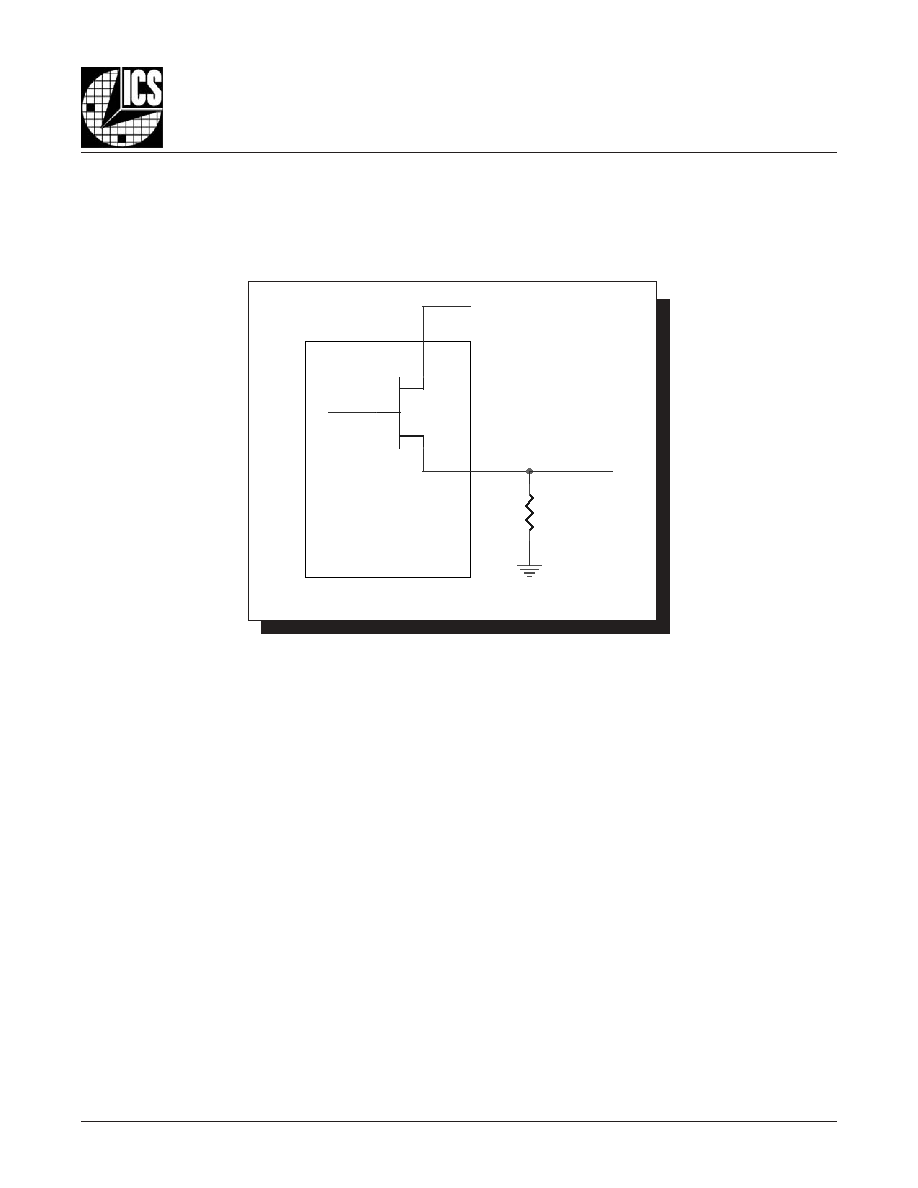
3. Calculations and Equations.
The purpose of this section is to derive the power dissipated into the load.
HSTL output driver circuit and termination are shown in
Figure 3.
T
o calculate worst case power dissipation into the load, use the following equations which assume a 50
load.
Pd_H is power dissipation when the output drives high.
Pd_L is the power dissipation when the output drives low.
Pd_H = (V
OH_M
AX
/R
L
) * (V
DD_MAX
- V
OH_M
AX
)
Pd_L = (V
OL_MAX
/R
L
) * (V
DD_MAX
- V
OL_MAX
)
Pd_H = (1.4V/50
) * (3.465V - 1.4V) = 57.82mW
Pd_L = (0.4V/50
) * (3.465V - 0.4V) = 24.52mW
Total Power Dissipation per output pair = Pd_H + Pd_L = 82.34mW
F
IGURE
3. HSTL D
RIVER
C
IRCUIT
AND
T
ERMINATION
V
DD
V
OUT
RL
50
Q1

85222AM-01
www.icst.com/products/hiperclocks.html
REV. A NOVEMBER 15, 2005
10
Integrated
Circuit
Systems, Inc.
ICS85222-01
D
UAL
LVCMOS / LVTTL-
TO
-
D
IFFERENTIAL
HSTL T
RANSLATOR
R
ELIABILITY
I
NFORMATION
T
RANSISTOR
C
OUNT
The transistor count for ICS85222-01 is: 443
T
ABLE
6.
JA
VS
. A
IR
F
LOW
T
ABLE
8 L
EAD
SOIC
JA
by Velocity (Linear Feet per Minute)
0
200
500
Single-Layer PCB, JEDEC Standard Test Boards
153.3�C/W
128.5�C/W
115.5�C/W
Multi-Layer PCB, JEDEC Standard Test Boards
112.7�C/W
103.3�C/W
97.1�C/W
NOTE: Most modern PCB designs use multi-layered boards. The data in the second row pertains to most designs.

85222AM-01
www.icst.com/products/hiperclocks.html
REV. A NOVEMBER 15, 2005
11
Integrated
Circuit
Systems, Inc.
ICS85222-01
D
UAL
LVCMOS / LVTTL-
TO
-
D
IFFERENTIAL
HSTL T
RANSLATOR
P
ACKAGE
O
UTLINE
- M S
UFFIX
FOR
8 L
EAD
SOIC
T
ABLE
7. P
ACKAGE
D
IMENSIONS
Reference Document: JEDEC Publication 95, MS-012
L
O
B
M
Y
S
s
r
e
t
e
m
i
l
l
i
M
M
U
M
I
N
I
M
M
U
M
I
X
A
M
N
8
A
5
3
.
1
5
7
.
1
1
A
0
1
.
0
5
2
.
0
B
3
3
.
0
1
5
.
0
C
9
1
.
0
5
2
.
0
D
0
8
.
4
0
0
.
5
E
0
8
.
3
0
0
.
4
e
C
I
S
A
B
7
2
.
1
H
0
8
.
5
0
2
.
6
h
5
2
.
0
0
5
.
0
L
0
4
.
0
7
2
.
1
�
0
�
8

85222AM-01
www.icst.com/products/hiperclocks.html
REV. A NOVEMBER 15, 2005
12
Integrated
Circuit
Systems, Inc.
ICS85222-01
D
UAL
LVCMOS / LVTTL-
TO
-
D
IFFERENTIAL
HSTL T
RANSLATOR
T
ABLE
8. O
RDERING
I
NFORMATION
While the information presented herein has been checked for both accuracy and reliability, Integrated Circuit Systems, Incorporated (ICS) assumes no responsibility for either its use
or for infringement of any patents or other rights of third parties, which would result from its use. No other circuits, patents, or licenses are implied. This product is intended for use
in normal commercial applications. Any other applications such as those requiring extended temperature range, high reliability, or other extraordinary environmental requirements are
not recommended without additional processing by ICS. ICS reserves the right to change any circuitry or specifications without notice. ICS does not authorize or warrant any ICS
product for use in life support devices or critical medical instruments.
The aforementioned trademark, HiPerClockS is a trademark of Integrated Circuit Systems, Inc. or its subsidiaries in the United States and/or other countries.
r
e
b
m
u
N
r
e
d
r
O
/
t
r
a
P
g
n
i
k
r
a
M
e
g
a
k
c
a
P
e
g
a
k
c
a
P
g
n
i
p
p
i
h
S
e
r
u
t
a
r
e
p
m
e
T
1
0
-
M
A
2
2
2
5
8
S
C
I
1
0
A
2
2
2
5
C
I
O
S
d
a
e
L
8
e
b
u
t
C
�
0
7
o
t
C
�
0
T
1
0
-
M
A
2
2
2
5
8
S
C
I
1
0
A
2
2
2
5
C
I
O
S
d
a
e
L
8
l
e
e
r
&
e
p
a
t
0
0
5
2
C
�
0
7
o
t
C
�
0
F
L
1
0
-
M
A
2
2
2
5
8
S
C
I
L
1
0
A
2
2
2
5
C
I
O
S
"
e
e
r
F
-
d
a
e
L
"
d
a
e
L
8
e
b
u
t
C
�
0
7
o
t
C
�
0
T
F
L
1
0
-
M
A
2
2
2
5
8
S
C
I
L
1
0
A
2
2
2
5
C
I
O
S
"
e
e
r
F
-
d
a
e
L
"
d
a
e
L
8
l
e
e
r
&
e
p
a
t
0
0
5
2
C
�
0
7
o
t
C
�
0
.
t
n
a
il
p
m
o
c
S
H
o
R
e
r
a
d
n
a
n
o
i
t
a
r
u
g
i
f
n
o
c
e
e
r
F
-
b
P
e
h
t
e
r
a
r
e
b
m
u
n
t
r
a
p
e
h
t
o
t
x
i
f
f
u
s
"
F
L
"
n
a
h
t
i
w
d
e
r
e
d
r
o
e
r
a
t
a
h
t
s
t
r
a
P
:
E
T
O
N
85222AM-01
www.icst.com/products/hiperclocks.html
REV. A NOVEMBER 15, 2005
13
Integrated
Circuit
Systems, Inc.
ICS85222-01
D
UAL
LVCMOS / LVTTL-
TO
-
D
IFFERENTIAL
HSTL T
RANSLATOR
T
E
E
H
S
Y
R
O
T
S
I
H
N
O
I
S
I
V
E
R
v
e
R
e
l
b
a
T
e
g
a
P
e
g
n
a
h
C
f
o
n
o
i
t
p
i
r
c
s
e
D
e
t
a
D
A
8
T
6
1
1
d
e
d
n
E
e
l
g
n
i
S
t
p
e
c
c
A
o
t
t
u
p
n
I
l
a
i
t
n
e
r
e
f
f
i
D
e
h
t
g
n
i
r
i
W
"
,
e
t
o
N
n
o
i
t
a
c
il
p
p
A
d
e
d
d
A
.
"
s
l
e
v
e
L
.
r
e
b
m
u
n
t
r
a
p
e
e
r
F
-
d
a
e
L
d
e
d
d
a
-
e
l
b
a
T
n
o
i
t
a
m
r
o
f
n
I
g
n
i
r
e
d
r
O
5
0
/
1
1
/
1
A
8
T
1
6
9
-
8
2
1
.
t
e
ll
u
b
e
e
r
f
-
d
a
e
l
d
e
d
d
A
d
e
d
d
A
.
s
n
i
P
t
u
p
t
u
O
d
n
a
t
u
p
n
I
d
e
s
u
n
U
r
o
f
s
n
o
i
t
a
d
n
e
m
m
o
c
e
R
.
n
o
i
t
a
l
u
c
l
a
c
n
o
i
t
a
p
i
s
s
i
D
r
e
w
o
P
,
s
n
o
i
t
a
r
e
d
i
s
n
o
C
r
e
w
o
P
d
e
t
c
e
r
r
o
C
.
e
t
o
n
e
e
r
f
-
d
a
e
l
d
n
a
y
t
i
t
n
a
u
q
l
e
e
r
&
e
p
a
t
d
e
d
d
a
-
e
l
b
a
T
n
o
i
t
a
m
r
o
f
n
I
g
n
i
r
e
d
r
O
5
0
/
5
1
/
1
1