 | –≠–ª–µ–∫—Ç—Ä–æ–Ω–Ω—ã–π –∫–æ–º–ø–æ–Ω–µ–Ω—Ç: 552-01B | –°–∫–∞—á–∞—Ç—å:  PDF PDF  ZIP ZIP |

ICS552-01B
Dual 1 to 4 High Speed Clock Buffer
MDS 552-01 B D
1
Revision 021500
Printed 11/14/00
Integrated Circuit Systems ∑ 525 Race Street ∑ San Jose ∑ CA ∑ 95126 ∑ (408)295-9800 tel ∑ www.icst.com
The ICS552-01B is a low cost, high speed clock
buffer which includes two identical single input to
four output buffers. By combining the two buffers
on one monolithic device, the propagation delays
are matched through the device, maintaining any
skew relationship present on the inputs. It is also
possible to connect the inputs together, creating a
one-to-eight buffer. See the ICS551M for a single
1 to 4 buffer in an 8 pin SOIC. For more than
eight outputs, see the MK74CBxxx BuffaloTM
series of clock drivers.
ICS also makes many PLL-based low skew output
devices, as well as Zero Delay Buffers to
synchronize clocks. Contact us for all of your
clocking needs.
Block Diagram
Description
Features
∑ Packaged in 20 pin narrow (150 mil) SSOP (QSOP)
∑ Up to 200 MHz clock input/output at 3.3 V
∑ Low skew of 250 ps maximum for any bank of four
∑ Inputs can be connected together for a 1 to 8 buffer
with 250 ps skew between any outputs
∑ 3.0V to 5.5V operating voltage
∑ Non-inverting
∑ Ideal for networking clocks
∑ Output Enable mode tri-states outputs
∑ Full CMOS output swing with 25 mA output drive
capability at TTL levels
∑ Advanced, low power, sub-micron CMOS process
∑ Industrial temperature version available
QA2
QA3
QA4
QB1
QB2
QA1
QB3
QB4
Control Logic
INA
INB
S1
S0
ICS552-01B
Dual 1 to 4 High Speed Clock Buffer
MDS 552-01 B D
2
Revision 021500
Printed 11/14/00
Integrated Circuit Systems ∑ 525 Race Street ∑ San Jose ∑ CA ∑ 95126 ∑ (408)295-9800 tel ∑ www.icst.com
Pin Descriptions
Key: CI = clock input with pull-up resistor; I = Input with internal pull-up resistor; O = Output;
P = power supply connection
Pin Assignment
Number
Name
Type
Description
1
INA
CI
Input to buffer A. Outputs QA1:QA4 will be the same frequency. Internal pull-up resistor.
2
DC
-
Don't Connect. Do not connect anything to this pin.
3
DC
-
Don't Connect. Do not connect anything to this pin.
4
VDD
P
Connect to +3.3 V or +5 V. Must be same as other VDDs.
5
VDD
P
Connect to +3.3 V or +5 V. Must be same as other VDDs.
6
GND
P
Connect to ground.
7
QA1
O
Output 1 from buffer A.
8
QA2
O
Output 2 from buffer A.
9
QA3
O
Output 3 from buffer A.
10
QA4
O
Output 4 from buffer A.
11
S1
I
Mode select pin 1. Selects mode for outputs. Must be at GND for all clocks on. Internal pull-up.
12
QB1
O
Output 1 from buffer B.
13
QB2
O
Output 2 from buffer B.
14
GND
P
Connect to ground.
15
VDD
P
Connect to +3.3 V or +5 V. Must be same as other VDDs.
16
VDD
P
Connect to +3.3 V or +5 V. Must be same as other VDDs.
17
QB3
O
Output 3 from buffer B.
18
QB4
O
Output 4 from buffer B.
19
INB
CI
Input to buffer B. Outputs QB1:QB4 will be the same frequency. Internal pull-up resistor.
20
S0
I
Mode select pin 0. Selects mode for outputs. Must be at GND for all clocks on. Internal pull-up.
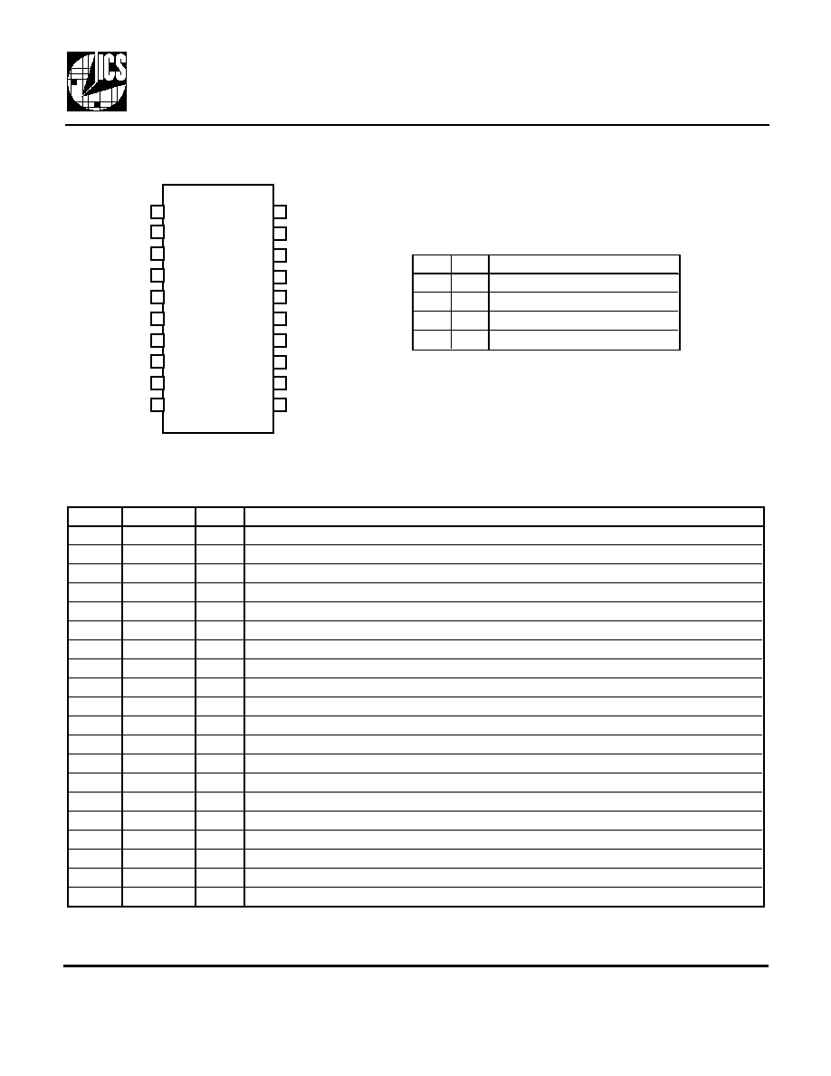
1
16
2
3
4
15
14
13
VDD
QA3
DC
VDD
20 pin (150 mil) SSOP
5
6
7
8
12
11
10
9
QA4
INB
DC
INA
QB4
S0
QB3
QB1
S1
QA2
QA1
18
17
19
20
GND
VDD
QB2
GND
VDD
S1
S0
MODE
0
0
QA1:4 and QB1:4 running.
0
1
Test mode.
1
0
OE. All outputs in high impedance.
1
1
QA1:4 only. QB1:4 stopped low.
Clock Output Select Table
0 = connect directly to GND
1 = connect directly to VDD

ICS552-01B
Dual 1 to 4 High Speed Clock Buffer
MDS 552-01 B D
3
Revision 021500
Printed 11/14/00
Integrated Circuit Systems ∑ 525 Race Street ∑ San Jose ∑ CA ∑ 95126 ∑ (408)295-9800 tel ∑ www.icst.com
Parameter
Conditions
Minimum
Typical
Maximum
Units
ABSOLUTE MAXIMUM RATINGS (note 1)
ABSOLUTE MAXIMUM RATINGS (note 1)
Supply voltage, VDD
Referenced to GND
7
V
Inputs and Clock Outputs
Referenced to GND
-0.5
VDD+0.5
V
Ambient Operating Temperature
ICS552R-01
0
70
∞C
ICS552R-01I
-40
85
∞C
Soldering Temperature
Max of 20 seconds
260
∞C
Storage temperature
-65
150
∞C
DC CHARACTERISTICS (VDD = 5.0 V unless noted)
DC CHARACTERISTICS (VDD = 5.0 V unless noted)
Operating Voltage, VDD
3
5.5
V
Input High Voltage, VIH, INA and INB
VDD/2 + 1
VDD/2
V
Input Low Voltage, VIL, X1 pin only
VDD/2
VDD/2 - 1
V
Input High Voltage, VIH, S1 and S0
2
V
Input Low Voltage, VIL, S1 and S0
0.8
V
Output High Voltage, VOH, 5V
IOH=-25mA
2.4
V
Output Low Voltage, VOL, 5V
IOL=25mA
0.4
V
Output High Voltage, VOH, CMOS level
IOH=-8mA
VDD-0.4
V
Operating Supply Current, IDD, 3.3V
No Load, all 135 MHz
35
mA
Short Circuit Current, 3.3V
Each output
±50
mA
Input capacitance
All inputs
4
pF
Internal pull-up resistor
All inputs
200
k
AC CHARACTERISTICS (VDD = 5.0 V unless noted)
AC CHARACTERISTICS (VDD = 5.0 V unless noted)
Input Frequency
0
200
MHz
Output Frequency, 3.3 V
10 pF load. Note 4.
200
MHz
15 pF load. Note 4.
180
MHz
Output Frequency, 5 V
15 pF load. Note 4.
135
MHz
Output Clock Rise Time
0.8 to 2.0V
1.5
ns
Output Clock Fall Time
2.0 to 0.8V
1.5
ns
Propagation Delay
At 3.3 V
4
ns
At 5.0 V
3
ns
Output to output skew within bank of four
Rising edges at VDD/2
250
ps
Output to output skew between banks
Note 2
250
ps
Electrical Specifications
Notes:
1. Stresses beyond those listed under Absolute Maximum Ratings could cause permanent damage to the device. Prolonged
exposure to levels above the operating limits but below the Absolute Maximums may affect device reliability.
2. When INA is connected to INB, all eight outputs are within 250 ps skew.
3. Duty cycle on outputs will match incoming clock duty cycle. Consult ICS for tight duty cycle clock generators.
4. With external series resistor of 33
positioned close to each output pin.

While the information presented herein has been checked for both accuracy and reliability, Integrated Circuit Systems, Inc (ICS) assumes no responsibility for either its use or for
the infringement of any patents or other rights of third parties, which would result from its use. No other circuits, patents, or licenses are implied. This product is intended for use
in normal commercial applications. Any other applications such as those requiring extended temperature range, high reliability, or other extraordinary environmental
requirements are not recommended without additional processing by ICS. ICS reserves the right to change any circuitry or specifications without notice. ICS does not authorize
or warrant any ICS product for use in life support devices or critical medical instruments.
ICS552-01B
Dual 1 to 4 High Speed Clock Buffer
MDS 552-01 B D
4
Revision 021500
Printed 11/14/00
Integrated Circuit Systems ∑ 525 Race Street ∑ San Jose ∑ CA ∑ 95126 ∑ (408)295-9800 tel ∑ www.icst.com
Ordering Information
Part/Order Number
Marking
Shipping packaging
Package
Temperature
ICS552R-01
ICS552R-01
tubes
20 pin SSOP
0 to 70∞C
ICS552R-01T
ICS552R-01
tape and reel
20 pin SSOP
0 to 70∞C
ICS552R-01I
ICS552R-01I
tubes
20 pin SSOP
-40 to 85∞C
ICS552R-01IT
ICS552R-01I
tape and reel
20 pin SSOP
-40 to 85∞C
External Components
The ICS552-01B requires a minimum number of external components for proper operation. Decoupling
capacitors of 0.01µF should be connected between VDD and GND on pins 4 and 6, and 16 and 14, as
close to the chip as possible. Other VDDs can be connected to these VDDs or the power plane. A series
termination resistor of 33
should be used for each clock output.
b
D
E1
E
e
A1
c
A
L
INDEX
AREA
1
2
Package Outline and Package Dimensions
(
For current dimensional specifications, see JEDEC Publication No. 95.)
20 pin SSOP
Inches
Inches
Millimeters
Millimeters
Symbol
Min
Max
Min
Max
A
0.053
0.069
1.35
1.75
A1
0.004
0.010
0.10
0.25
b
0.008
0.012
0.20
0.30
c
0.007
0.010
0.18
0.25
D
0.337
0.344
8.55
8.75
e .025 BSC
.025 BSC
0.635 BSC
0.635 BSC
E
0.228
0.244
5.80
6.20
E1
0.150
0.157
3.80
4.00
L
0.016
0.050
0.40
1.27