ICS552A-01
MDS 552A-01 B
1
Revision 010906
Integrated Circuit Systems, Inc.
525 Race Street, San Jose, CA 95126
tel (408) 297-1201
www.icst.com
Oscillator, Multiplier, and Buffer with 8 Outputs
Description
The ICS552A-01 produces 8 low-skew copies of the
multiple input clock or fundamental, parallel-mode
crystal. Unlike other clock drivers, these parts do not
require a separate oscillator for the input. Using ICS'
patented Phase-Locked Loop (PLL) to multiply the
input frequency, it is ideal for generating and
distributing multiple high-frequency clocks. This is a
single chip used for 3 different applications:
1) ICS552A-01 (A mode) -- an Oscillator mutiplier
2) ICS552A-01 (B mode) -- a Dual 1:4 buffer
3) ICS552A-01 (C mode) -- a 1:8 Oscillator buffer
Features (all)
�
Packaged as 20-pin SSOP (QSOP)
�
Pb-free packaging available
�
Operating voltages of 3.0 V to 5.5 V
�
Industrial temperature available
Features (specific)
ICS552A-01 (for A mode)
�
Contains on-chip multiplier with selections of x1,
x1.33, x2, x2.66, x3, x3.33, x4, x4.66, x5, and x6
�
Power-down and Tri-state modes
ICS552A-01 (for B mode)
�
Up to 200 MHz clock input/output at 3.3 V
�
Low skew of 250 ps maximum for any bank of four
�
Inputs can be connected together for a 1 to 8 buffer
with 250 ps skew between any outputs
�
Non-inverting buffer mode
�
Ideal for clock networks
�
Output Enable mode tri-states outputs
�
Full CMOS output swing with 25 mA output drive
capability at TTL levels
�
Advanced, low power, sub-micron CMOS process
ICS552A-01 (for C mode)
�
Use with 25 MHz crystal for networking
�
Use with 27 MHz crystal for MPEG
ICS552A-01 (for A and C modes)
�
Input frequency of 10.0 to 27.0 MHz
�
Provides 8 low-skew outputs (<250 ps)
�
Output clock duty cycle of 40/60 at 3.3 V
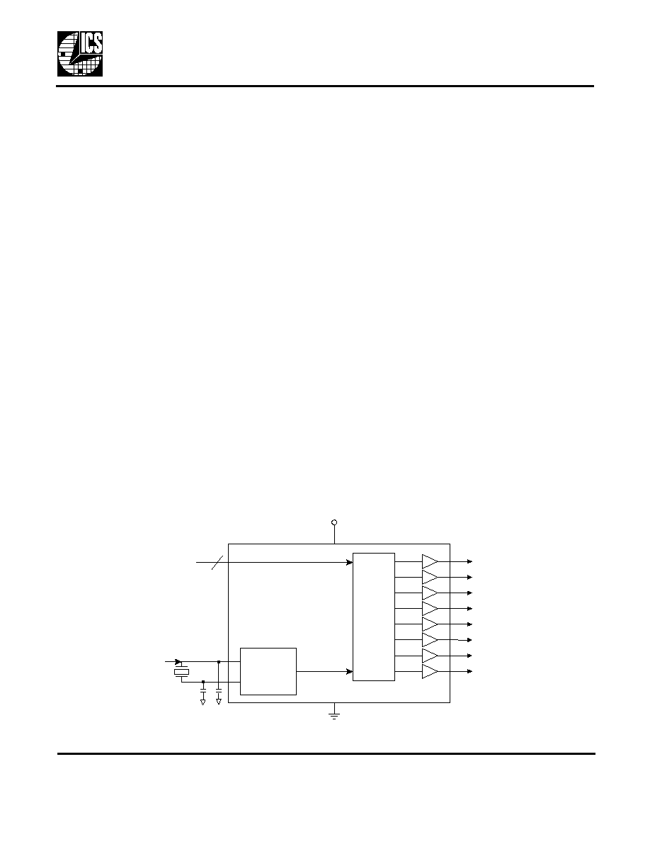
Block Diagram
(ICS552A-01--A mode)
Crystal
Buffer/
Crystal
Oscillator
GND
VDD
PLL
Multiplier
S3:S0
CLK1
CLK8
CLK7
CLK6
CLK5
CLK4
CLK3
CLK2
4
X2
10.0 to 27.0 MHz
crystal or clock input
External capacitors are
required with a crystal input.
X1
Oscillator, Multiplier, and Buffer with 8 Outputs
MDS 552A-01 B
2
Revision 010906
Integrated Circuit Systems, Inc.
525 Race Street, San Jose, CA 95126
tel (408) 297-1201
www.icst.com
ICS552A-01
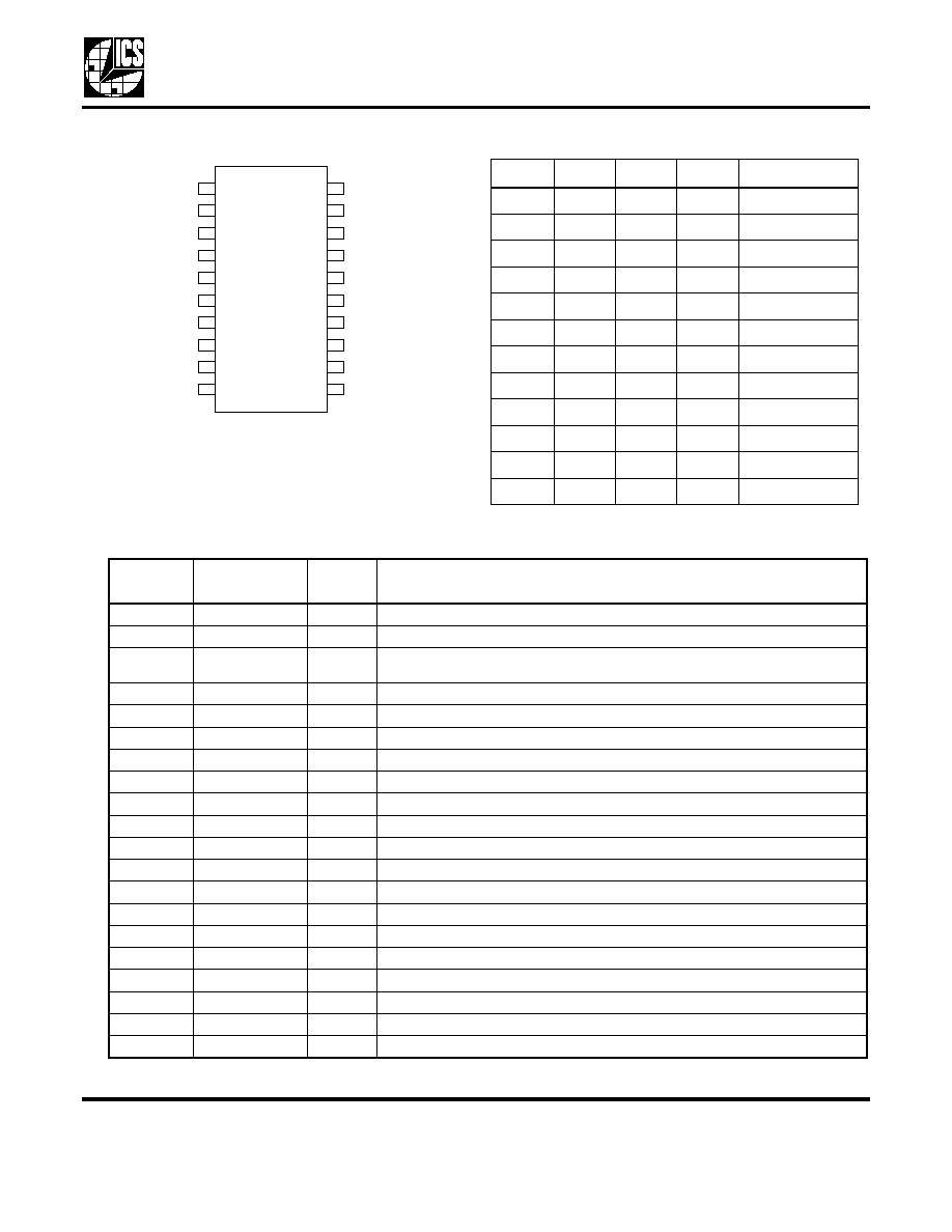
Pin Assignment
(ICS552A-01--A mode)
Multiplier Select Table
Pin Descriptions
(ICS552A-01--A mode)
16
1
15
2
14
DC
S0
3
13
X2
4
12
X1/ICLK
DC
5
11
S2
6
7
VDD
8
GND
S3
VDD
GND
CLK1
CLK5
CLK2
CLK6
9
10
CLK3
CLK7
CLK4
CLK8
20
19
18
17
20-pin (150 mil) SSOP (QSOP)
S1
S3
S2
S1
S0
Multiplier
0
0
0
0
Power Down
0
0
0
1
x1
0
0
1
0
x1.333
0
0
1
1
x2
0
1
0
0
x2.666
0
1
0
1
x3
0
1
1
0
x3.333
0
1
1
1
x4
1
0
0
0
x5
1
0
0
1
x4.66
1
0
1
0
x6
1
1
0
1
Tri-state all
Pin
Number
Pin
Name
Pin
Type
Pin Description
1
DC
--
Do not connect.
2
X2
XO
Crystal connection. Connect to a 10 - 27 MHz fundamental mode crystal.
3
X1/ICLK
XI
Crystal connection. Connect to a 10 - 27 MHz fundamental mode crystal or
clock.
4
VDD
Power
Connect to +3.3 V or 5 V. Decouple with pin 6. Must be same as other VDDs.
5
S2
Input
Multiplier Select pin 2 per table above.
6
GND
Power
Connect to ground.
7
CLK1
Output
Output clock 1.
8
CLK2
Output
Output clock 2.
9
CLK3
Output
Output clock 3.
10
CLK4
Output
Output clock 4.
11
S1
Input
Multiplier Select pin 1 per table above
12
CLK5
Output
Output clock 5.
13
CLK6
Output
Output clock 6.
14
GND
Power
Connect to ground.
15
S3
Input
Multiplier Select pin 3 per table above
16
VDD
Power
Connect to +3.3 V or 5 V. Decouple with pin 14. Must be same as other VDDs.
17
CLK7
Output
Output clock 7.
18
CLK8
Output
Output clock 8.
19
DC
--
Do not connect.
20
S0
Input
Multiplier Select pin 0 per table above
Oscillator, Multiplier, and Buffer with 8 Outputs
MDS 552A-01 B
3
Revision 010906
Integrated Circuit Systems, Inc.
525 Race Street, San Jose, CA 95126
tel (408) 297-1201
www.icst.com
ICS552A-01
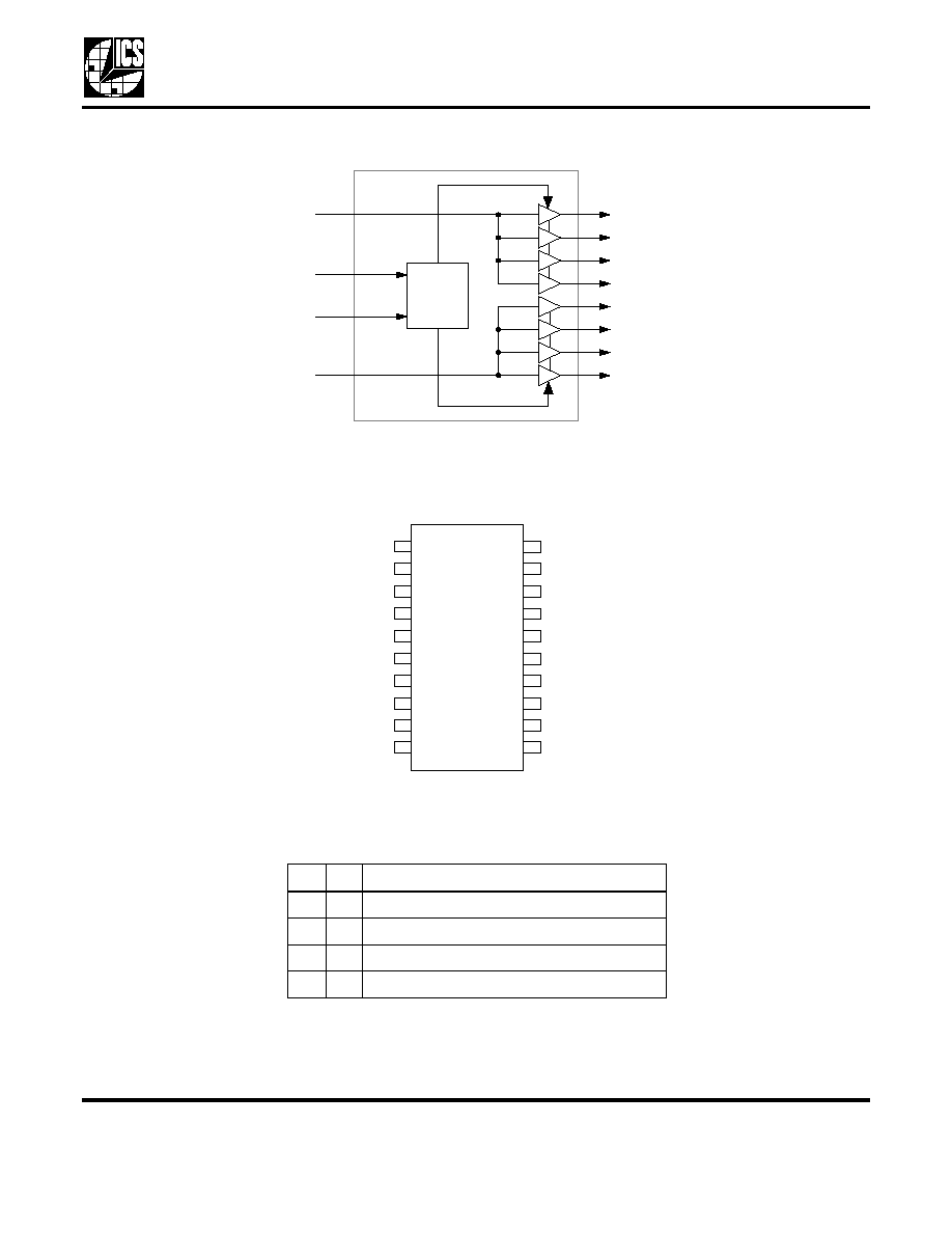
Block Diagram
(ICS552A-01--B mode)
Pin Assignment
(ICS552A-01--B mode)
Clock Output Select Table
(ICS552A-01--B mode)
S1
S0
Mode
0
0
QA1:4 and QB1:4 running
0
1
Test mode
1
0
OE. All outputs in high impedance
1
1
QA1:4 only. QB1:4 stopped low
Control
Logic
INA
QA1
QB4
QB3
QB2
QB1
QA4
QA3
QA2
INB
S1
S0
16
1
15
2
14
INA
S0
3
13
DC
4
12
DC
INB
5
11
VDD
6
7
VDD
8
GND
VDD
VDD
GND
QA1
QB1
QA2
QB2
9
10
QA3
QB3
QA4
QB4
20
19
18
17
20-pin (150 mil) SSOP (QSOP)
S1

Oscillator, Multiplier, and Buffer with 8 Outputs
MDS 552A-01 B
4
Revision 010906
Integrated Circuit Systems, Inc.
525 Race Street, San Jose, CA 95126
tel (408) 297-1201
www.icst.com
ICS552A-01
Pin Descriptions
(ICS552A-01--B mode)
KEY: CI = clock input with pull-up resistor; I = input with internal pull-up resistor.
Pin
Number
Pin
Name
Pin
Type
Pin Description
1
INA
CI
Input to buffer A. Outputs QA1:4 will be the same frequency. Internal pull-up resistor.
2
DC
--
Do not connect.
3
DC
--
Do not connect.
4
VDD
Power
Connect to +3.3 V or 5.0 V. Must be same as other VDDs.
5
VDD
Power
Connect to +3.3 V or 5.0 V. Must be same as other VDDs.
6
GND
Power
Connect to ground.
7
QA1
Output
Output 1 from buffer A.
8
QA2
Output
Output 2 from buffer A.
9
QA3
Output
Output 3 from buffer A.
10
QA4
Output
Output 4 from buffer A.
11
S1
I
Mode Select pin 1. Selects mode for outputs. Must be at GND for all clocks on. Internal
pull-up resistor.
12
QB1
Output
Output 1 from buffer B.
13
QB2
Output
Output 2 from buffer B.
14
GND
Power
Connect to ground.
15
VDD
Power
Connect to +3.3 V or 5.0 V. Must be same as other VDDs.
16
VDD
Power
Connect to +3.3 V or 5.0 V. Must be same as other VDDs.
17
QB3
Output
Output 3 from buffer B.
18
QB4
Output
Output 4 from buffer B.
19
INB
CI
Input to buffer B. Outputs QA1:4 will be the same frequency. Internal pull-up resistor.
20
S0
I
Mode Select pin 0. Selects mode for outputs. Must be at GND for all clocks on. Internal
pull-up resistor.
Oscillator, Multiplier, and Buffer with 8 Outputs
MDS 552A-01 B
5
Revision 010906
Integrated Circuit Systems, Inc.
525 Race Street, San Jose, CA 95126
tel (408) 297-1201
www.icst.com
ICS552A-01
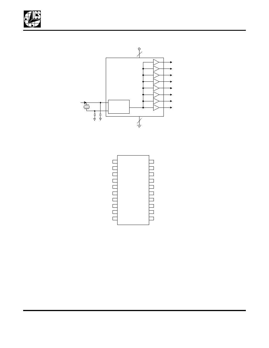
Block Diagram
(ICS552A-01--C mode)
Pin Assignment
(ICS552A-01--C mode)
Crystal
Oscillator
GND
VDD
CLK1
CLK8
CLK7
CLK6
CLK5
CLK4
CLK3
CLK2
5
X2
10.0 to 27.0 MHz
crystal input
External capacitors are
required with a crystal input.
X1
3
16
1
15
2
14
DC
VDD
3
13
X2
4
12
X1
DC
5
11
GND
6
7
VDD
8
GND
VDD
VDD
GND
CLK1
CLK5
CLK2
CLK6
9
10
CLK3
CLK7
CLK4
CLK8
20
19
18
17
20-pin (150 mil) SSOP (QSOP)
VDD