ICS601-25
MDS 601-25 C
1
Revision 071505
I n t e gra t e d C i r c u i t S y s t e m s
5 2 5 R a c e S t r e e t , S a n J o s e, C A 9 5 1 2 6
t e l ( 4 0 8 ) 2 9 7 - 1 2 0 1
w w w. i c s t . c o m
L
OW
P
HASE
N
OISE
1
TO
5 C
LOCK
M
ULTIPLIER
Description
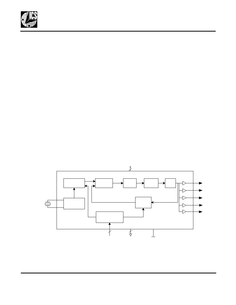
The ICS601-25 is a low-cost, low phase noise, high
performance clock synthesizer for applications which
require low phase noise, low jitter, and low skew fanout.
It is ICS' lowest phase noise multiplier, and also the
lowest CMOS part in the industry. Using ICS' patented
analong and digital Phase Locked Loop (PLL)
techniques, the chip accepts a 10-27 MHz crystal or
clock input, and produces output clocks up to 156 MHz.
Features
∑
Packaged in 20-pin SSOP
∑
Uses fundamental 10 - 27 MHz crystal or clock
∑
Output clocks up to 156 MHz
∑
Low phase noise: -132 dBc/Hz at 10 kHz
∑
Five low skew (<250 ps) outputs
∑
Low jitter - 18 ps one sigma at 125 MHz
∑
Full swing CMOS outputs with 25 mA drive capability
at TTL levels
∑
Powerdown mode lowers power consumption
∑
Advanced, low power, sub-micron CMOS process
∑
Industrial temperature version available
∑
Available in Pb (lead) free package
∑
Operating voltage of 3.3 V
Block Diagram
CLK1
ROM Based
Multipliers
VCO
Divide
X1/ICLK
X2
Crystal or
clock input
Crystal
Oscillator
Reference
Divider
Phase
Comparator
VDD
Charge
Pump
Loop
Filter
VCO
S3:0
PD
CLK5
CLK4
CLK3
CLK2
5
GND
3
4

L
OW
P
HASE
N
OISE
1
TO
5 C
LOCK
M
ULTIPLIER
MDS 601-25 C
2
Revision 071505
I n t e gr a t e d C i r c u i t S y s t e m s
5 2 5 R a c e S t r e e t , S a n J o s e, C A 9 5 1 2 6
t e l ( 4 0 8 ) 2 9 7 - 1 2 0 1
w w w. i c s t . c o m
ICS601-25
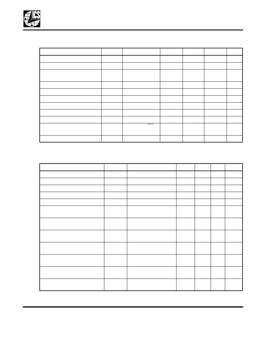
Pin Assignment
Output Select Table
Pin Descriptions
5
GND
6
7
8
9
10
CLK3
GND
VDD
PD
S3
CLK1
VDD
S1
S2
CLK5
CLK4
16
15
14
13
12
11
20 Pin (150 mil) SSOP
3
4
VDD
CLK2
VDD
18
S0
17
1
2
VDD
GND
X2
20
X1/ICLK
19
S3
S2
S1
S0
Multiplier
0
0
0
0
x1
0
0
0
1
x2
0
0
1
0
x3
0
0
1
1
x4
0
1
0
0
x5
0
1
0
1
x6
0
1
1
0
x8
0
1
1
1
x16
1
0
0
0
x7
1
0
0
1
x9
1
0
1
0
x10
1
0
1
1
x11
1
1
0
0
x12
1
1
0
1
output tristates
1
1
1
0
x14
1
1
1
1
x15
Pin
Number
Pin
Name
Pin
Type
Pin Description
1
X1/ICLK
XI
Crystal or clock input. Connect to a 10-27 MHz fundamental parallel mode
crystal or clock input.
2
VDD
Power
Connect to +3.3 V.
3
S0
Input
Select pin 0. Internal pull-up.
4, 5
VDD
Power
Connect to +3.3 V.
6
S1
Input
Select pin 1. Internal pull-up.
7
GND
Power
Connect to ground.
8
S3
Input
Select pin 3. Internal pull-down.
9
PD
Input
Powerdown when held low. Internal pull-up.
10
S2
Input
Select pin 2. Internal pull-up.
11
CLK1
Output
Clock output.
12
VDD
Power
Connect to +3.3 V.
13
CLK5
Output
Clock output.
14
CLK4
Output
Clock output.
15
GND
Power
Connect to ground.
16
CLK3
Output
Clock output.
17
CLK2
Output
Clock output.
18
VDD
Power
Connect to +3.3 V.
19
GND
Power
Connect to ground.
20
X2
XO
Crystal connection. Connect to a 10-27 MHz fundamental parallel mode
crystal or leave unconnected for clock input.

L
OW
P
HASE
N
OISE
1
TO
5 C
LOCK
M
ULTIPLIER
MDS 601-25 C
3
Revision 071505
I n t e gr a t e d C i r c u i t S y s t e m s
5 2 5 R a c e S t r e e t , S a n J o s e, C A 9 5 1 2 6
t e l ( 4 0 8 ) 2 9 7 - 1 2 0 1
w w w. i c s t . c o m
ICS601-25
External Components
The ICS601-25 requires a minimum number of external components for proper operation. Decoupling
capacitors of 0.01
µF and 0.1 µF should be connected between VDD and GND, as close to the part as
possible. A 33
series terminating resistor should be used on each clock output. The crystal must be
connected as close to the chip as possible. The crystal should be fundamental mode, parallel resonant. Do
not use third overtone. For exact tuning when using a crystal, capacitors should be connected from pins X1
to ground and X2 to ground. In general, the value of these capacitors is given by the following equation,
where CL is the crystal load capacitance: Crystal caps (pF) = (CL-5) x 2. So for a crystal with 16 pF load
capacitance, two 22 pF caps can be used. For any given board layout, ICS can measure the board
capacitance and recommend the exact capacitance value to use.
Absolute Maximum Ratings
Stresses above the ratings listed below can cause permanent damage to the ICS601-25. These ratings,
which are standard values for ICS commercially rated parts, are stress ratings only. Functional operation of
the device at these or any other conditions above those indicated in the operational sections of the
specifications is not implied. Exposure to absolute maximum rating conditions for extended periods can
affect product reliability. Electrical parameters are guaranteed only over the recommended operating
temperature range.
Recommended Operation Conditions
DC Electrical Characteristics
VDD=3.3 V ±10%
, Ambient temperature -40 to +85
∞C
Item
Rating
Supply Voltage, VDD
7 V
All Inputs and Outputs
-0.5 V to VDD+0.5 V
Ambient Operating Temperature, Commercial version
0 to +70
∞C
Ambient Operating Temperature, Industrial version
-40 to +85
∞C
Storage Temperature
-65 to +150
∞C
Junction Temperature
125
∞C
Soldering Temperature
260
∞C
Parameter
Min.
Typ.
Max.
Units
Ambient Operating Temperature (commercial)
0
+70
∞C
Ambient Operating Temperature (industrial)
-40
+85
∞C
Power Supply Voltage (measured in respect to GND)
+2.97
+3.63
V
Parameter
Symbol
Conditions
Min.
Typ.
Max.
Units
Operating Voltage
VDD
2.97
3.63
V
Input High Voltage
V
IH
X1/ICLK pin only
VDD/2+1
V
Input Low Voltage
V
IL
X1/ICLK pin only
VDD/2-1
V
L
OW
P
HASE
N
OISE
1
TO
5 C
LOCK
M
ULTIPLIER
MDS 601-25 C
4
Revision 071505
I n t e gr a t e d C i r c u i t S y s t e m s
5 2 5 R a c e S t r e e t , S a n J o s e, C A 9 5 1 2 6
t e l ( 4 0 8 ) 2 9 7 - 1 2 0 1
w w w. i c s t . c o m
ICS601-25
DC Electrical Characteristics
(continued)
AC Electrical Characteristics
VDD = 3.3V ±10%
, Ambient Temperature -40 to +85
∞ C
Note 1: Measured with 15 pF load
Parameter
Symbol
Conditions
Min.
Typ.
Max.
Units
Input High Voltage
V
IH
2
VDD
V
Input Low Voltage
V
IL
0.8
V
Output High Voltage, CMOS
level
V
OH
I
OH
= -4 mA
VDD-0.4
V
Output High Voltage
V
OH
I
OL
= -12 mA
2.4
V
Output Low Voltage
V
OL
I
OL
= 12 mA
0.4
V
Operating Supply Current
IDD
No load, 125 MHz
45
60
mA
Short Circuit Current
I
OS
Each output
± 40
± 60
mA
Input Capacitance
Select pins
5
pF
Output Impedance
Z
OUT
20
On Chip Pull-up Resistor
R
PU
S2, S1, S0, PD
pins
510
k
On Chip Pull-down Resistor
R
PD
S3 pin
240
k
Parameter
Symbol
Conditions
Min.
Typ.
Max.
Units
Input Frequency
10
27
MHz
Output Frequency
At 3.3V
156
MHz
Output Rise Time
t
OR
0.8 to 2.0 V, Note 1
1.5
ns
Output Fall Time
t
OF
0.8 to 2.0 V, Note 1
1.5
ns
Output Clock Duty Cycle
At VDD/2, Note 1
45
50
55
%
Maximum Absolute jitter, short
term, 125 MHz
Note 1
±50
±75
ps
Maximum jitter, one sigma, 125
MHz (x5)
Note 1
18
25
ps
Phase Noise, relative to carrier,
125 MHz (x5)
100 Hz offset
-90
-95
dBc/Hz
Phase Noise, relative to carrier,
125 MHz (x5)
1 kHz
-115
-120
dBc/Hz
Phase Noise, relative to carrier,
125 MHz (x5)
10 kHz offset
-118
-123
dBc/Hz
Phase Noise, relative to carrier,
125 MHz (x5)
100 kHz offset
-115
-120
dBc/Hz
Output to Output Skew
25M in, 125M out,
Note 1
250
ps
L
OW
P
HASE
N
OISE
1
TO
5 C
LOCK
M
ULTIPLIER
MDS 601-25 C
5
Revision 071505
I n t e gr a t e d C i r c u i t S y s t e m s
5 2 5 R a c e S t r e e t , S a n J o s e, C A 9 5 1 2 6
t e l ( 4 0 8 ) 2 9 7 - 1 2 0 1
w w w. i c s t . c o m
ICS601-25
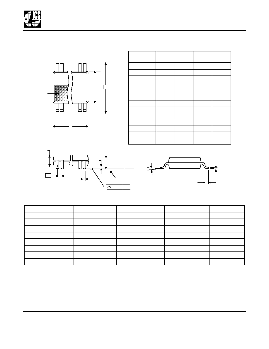
Package Outline and Package Dimensions
(20-pin SSOP, 150 Mil. Narrow Body)
Package dimensions are kept current with JEDEC Publication No. 95
Ordering Information
Parts that are ordered with a "LF" suffix to the part number are the Pb-Free configuration and are RoHS compliant.
While the information presented herein has been checked for both accuracy and reliability, Integrated Circuit Systems (ICS) assumes no
responsibility for either its use or for the infringement of any patents or other rights of third parties, which would result from its use. No other
circuits, patents, or licenses are implied. This product is intended for use in normal commercial applications. Any other applications such as those
requiring extended temperature range, high reliability, or other extraordinary environmental requirements are not recommended without
additional processing by ICS. ICS reserves the right to change any circuitry or specifications without notice. ICS does not authorize or warrant
any ICS product for use in life support devices or critical medical instruments.
Part / Order Number
Marking
Shipping Packaging
Package
Temperature
ICS601R-25
ICS601R-25
Tubes
20-pin SSOP
0 to +70
∞ C
ICS601R-25T
ICS601R-25
Tape and Reel
20-pin SSOP
0 to +70
∞ C
ICS601R-25I
ICS601R-25I
Tubes
20-pin SSOP
-40 to 85
∞ C
ICS601R-25IT
ICS601R-25I
Tape and Reel
20-pin SSOP
-40 to 85
∞ C
ICS601R-25LF
601R-25LF
Tubes
20-pin SSOP
0 to +70
∞ C
ICS601R-25LFT
601R-25LF
Tape and Reel
20-pin SSOP
0 to +70
∞ C
ICS601R-25ILF
601R-25ILF
Tubes
20-pin SSOP
-40 to 85
∞ C
ICS601R-25ILFT
601R-25ILF
Tape and Reel
20-pin SSOP
-40 to 85
∞ C
INDEX
AREA
1 2
20
D
E1
E
SEATING
PLANE
A1
A
A2
e
- C -
b
aaa
C
c
L
*For reference only. Controlling dimensions in mm.
Millimeters
Inches*
Symbol
Min
Max
Min
Max
A
1.35
1.75
.0532
.0688
A1
0.10
0.25
.0040
0.0098
A2
--
1.50
--
.059
b
0.20
0.30
0.008
0.012
C
0.18
0.25
.007
.010
D
8.55
8.75
.337
.344
E
5.80
6.20
.228
.244
E1
3.80
4.00
.1497
.1574
e
0.635 Basic
0.025 Basic
L
0.40
1.27
.016
.050
0
∞
8
∞
0
∞
8
∞
aaa
--
0.10
--
0.004