 | –≠–ª–µ–∫—Ç—Ä–æ–Ω–Ω—ã–π –∫–æ–º–ø–æ–Ω–µ–Ω—Ç: 620-01 | –°–∫–∞—á–∞—Ç—å:  PDF PDF  ZIP ZIP |

The ICS620-01 is a low cost, low jitter, high
performance clock synthesizer for digital still
cameras. Using analog Phase-Locked Loop
(PLL) techniques, the device uses a
14.318 MHz crystal input to produce multiple
output clocks required in the camera. It
provides selectable NTSC/PAL clock, a
selectable processor clock, a selectable CCD
clock, and a selectable interface clocks. Most
clocks are generated to a very low ppm
synthesis error rate.
All clocks can be turned off using a power
down mode. Custom versions with user-
defined frequencies and power down modes
are available in 6-8 weeks.
ICS620-01
Digital Still Camera Clock Source
MDS 620-01 B
1
Revision 072098 Printed 12/4/00
Integrated Circuit Systems ∑ 1271
Parkmoor Ave.∑San Jose∑CA∑95126∑(408)295-9800tel∑(408)295-9818fax
PRELIMINARY INFORMATION
I C R O
C
LOC K
Block Diagram
Description
Features
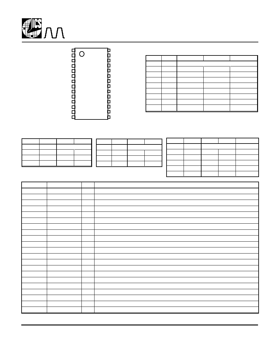
∑ Packaged in 28 pin, 150 mil wide SSOP (QSOP)
∑ Provides all clocks necessary for many digital still
camera systems
∑ All clocks are frequency locked together
∑ Interface clock for USB, P1394, or UART
∑ Saves space over multiple crystals and oscillators
∑ Clocks power down when all select pins are low
∑ Full CMOS outputs also compatible with TTL levels
∑ +3.3 V or +5 V operation
∑ Low power, sub-micron CMOS process
∑ Custom versions available
Crystal
Oscillator
PLL Clock
Synthesis
Circuitry
CCD Clock 1
Processor Clock 1
2
NSEL1:0
14.31818
MHz
crystal
X1
X2
NTSC/PAL Clock 1
Interface Clock 2
Output
Buffer
PLL Clock
Synthesis
Circuitry
PLL Clock
Synthesis
Circuitry
PLL Clock
Synthesis
Circuitry
PSEL1:0
2
CSEL1:0
2
2
ISEL1:0
Output
Buffer
Output
Buffer
Output
Buffer
Interface Clock 1
CCD Clock 2
˜2
Output
Buffer
Output
Buffer
Output
Buffer
Output
Buffer
NTSC/PAL Clock 2
Processor Clock 2
˜2
˜2
ICS620-01
Digital Still Camera Clock Source
MDS 620-01 B
2
Revision 072098 Printed 12/4/00
Integrated Circuit Systems ∑ 1271
Parkmoor Ave.∑San Jose∑CA∑95126∑(408)295-9800tel∑(408)295-9818fax
PRELIMINARY INFORMATION
I C R O
C
LOC K
Pin Descriptions
Pin
Assignment
Key: I = Input, O = Output, P = Power supply connection, TI = tri-level input (automatically biased to M level if unconnected).
Internal pull-ups are on pins 6, 16, 20, 24, and 27.
Pin #
Name
Type Description
1
CSEL0
TI
C clock SELect pin 0.
2, 26
NC
-
No Connect. Nothing is connected internally to this pin.
3
X2
XO Crystal connection. Connect to a 14.31818 MHz crystal or input clock.
4
X1
XI
Crystal connection. Connect to a 14.31818 MHz crystal, or leave unconnected for clock.
5, 7, 8, 21
VDD
P
Connect to +3.3V or +5V. Must be same voltage on all pins.
6
NSEL1
I
NTSC/PAL SELect pin 1.
9
NSEL0
TI
NTSC/PAL SELect pin 0.
10, 11, 19, 23
GND
P
Connect to Ground.
12
CLKI2
O
Interface CLocK output 2.
13
CLKI1
O
Interface CLocK output 1.
14
CLKP2
O
Processor CLocK output 2.
15
CLKP1
O
Processor CLocK output 1.
16
PSEL1
I
Processor clock SELect pin 1.
17
CLKC2
O
C CLocK output 2.
18
CLKC1
O
C CLocK output 1.
20
PSEL0
I
Processor clock SELect pin 0.
22
CLKN2
O
NTSC/PAL CLocK output 2.
24
ISEL1
I
Interface clock SELect pin 1.
25
CLKN1
O
NTSC/PAL CLocK output 1. Output may stop high or low during power down.
27
ISEL0
I
Interface clock SELect pin 0.
28
CSEL1
TI
C clock SELect pin 1.
Processor Clock Select (MHz)
PSEL1
PSEL0 CLKP1 CLKP2
0
0
Power down both
Power down both
0
1
20.50
10.25
1
0
23.96
11.98
1
1
24.5455 12.2727
CSEL1 CSEL0
CLKC1
CLKC2
Actual error
0
0
Power Down - both outputs stop low
Power Down - both outputs stop low
Power Down - both outputs stop low
0
M
14.31818
7.15909
0 ppm
0
1
9.81818
4.90909
0 ppm
M
0
7.3728
3.6864
31 ppm high
M
M
27
13.5
0 ppm
M
1
8
4
0.017% high
1
0
28
14
0 ppm
1
M
24.54545
12.272725
11 ppm high
1
1
32
16
0.017% high
Clock C Frequency Select Table (MHz)
1
8
9
2
3
4
5
6
7
10
11
12
13
14
16
15
20
17
18
19
25
24
23
22
21
26
27
28
GND
NSEL0
X1
VDD
X2
VDD
NC
GND
CLKI2
CLKP1
ISEL0
GND
PSEL1
NC
CSEL1
GND
VDD
PSEL0
CLKI1
CSEL0
CLKC1
CLKC2
ISEL1
CLKN1
CLKP2
NSEL1
VDD
CLKN2
Interface Clock Select (MHz)
NSEL1 NSEL0 CLKN1 CLKN2
Error
0
0
Power down
Power down
0
M
8.8672 4.43361 2 ppm low
0
1
27
13.5
0 ppm
1
0
35.4688 17.7344 2 ppm low
1
M
7.1591
3.5795
0 ppm
1
1
28.6364 14.3182
0 ppm
ISEL1 ISEL0 CLKI1
CLKI2
0
0
Power down both
Power down both
0
1
36.864
18.432
1
0
24.576
8.192
1
1
48
12
NTSC/PAL Clock Select (MHz)
Key: 0 = connect to ground, 1 = connect to VDD,
M = leave unconnected (floating).
ICS620-01
Digital Still Camera Clock Source
MDS 620-01 B
3
Revision 072098 Printed 12/4/00
Integrated Circuit Systems ∑ 1271
Parkmoor Ave.∑San Jose∑CA∑95126∑(408)295-9800tel∑(408)295-9818fax
PRELIMINARY INFORMATION
I C R O
C
LOC K
Electrical Specifications
External Components
The ICS620-01 requires some inexpensive external components for proper operation. Decoupling capacitors of 0.1µF should be
connected on VDD pins 5, 7+8, and 21 to ground, as close to the ICS620-01 as possible. A series termination resistor of 33
should
be used for each clock output. The 14.31818 MHz crystal should be parallel resonant with an accuracy of 30ppm or better. For
tuning, the formula 2∑(C
L
-6) gives the value of each capacitor that should be connected between X1 and ground and X2 and ground,
where C
L
= the crystal load (or "correlation") capacitance.
Parameter
Conditions
Minimum
Typical
Maximum
Units
ABSOLUTE MAXIMUM RATINGS
Supply Voltage, VDD
Referenced to GND
7
V
Inputs and Clock Outputs
Referenced to GND
-0.5
VDD+0.5
V
Ambient Operating Temperature
0
70
∞C
Soldering Temperature
Max of 10 seconds
260
∞C
Storage temperature
-65
150
∞C
DC CHARACTERISTICS
Operating Voltage, VDD
3
5.5
V
Input High Voltage, VIH
Pins 6, 16, 20, 24, 27
2
V
Input Low Voltage, VIL
Pins 6, 16, 20, 24, 27
0.8
V
Input High Voltage, VIH
Pins 1, 9, 28
VDD-0.5
V
Input Mid-level Voltage
Pins 1, 9, 28
Leave pin unconnected or tri-stated
Leave pin unconnected or tri-stated
Leave pin unconnected or tri-stated
V
Input Low Voltage, VIL
Pins 1, 9, 28
0.5
V
Output High Voltage, VOH
IOH=-4mA
VDD-0.4
V
Output High Voltage, VOH
IOH=-25mA
2.4
V
Output Low Voltage, VOL
IOL=25mA
0.4
V
Operating Supply Current, IDD
No Load
TBD
mA
Short Circuit Current
Each output
±70
mA
On-Chip Pull-up Resistor
Pins 6, 16, 20, 24, 27
250
k
Input Capacitance
All inputs but X1
7
pF
AC CHARACTERISTICS
Input Frequency
14.31818
MHz
Output Clock Rise Time
0.8 to 2.0V
TBD
ns
Output Clock Fall Time
2.0 to 0.8V
TBD
ns
Output Clock Duty Cycle
at VDD/2
45
49 to 51
55
%
Absolute Jitter
TBD
ps
Note:
1. Stresses beyond those listed under Absolute Maximum Ratings could cause permanent damage to the device. Prolonged exposure
to levels above the operating limits but below the Absolute Maximums may affect device reliability.

ICS620-01
Digital Still Camera Clock Source
MDS 620-01 B
4
Revision 072098 Printed 12/4/00
Integrated Circuit Systems ∑ 1271
Parkmoor Ave.∑San Jose∑CA∑95126∑(408)295-9800tel∑(408)295-9818fax
PRELIMINARY INFORMATION
I C R O
C
LOC K
While the information presented herein has been checked for both accuracy and reliability, ICS Incorporated assumes no responsibility for either its use or for the infringement of
any patents or other rights of third parties, which would result from its use. No other circuits, patents, or licenses are implied. This product is intended for use in normal
commercial applications. Any other applications such as those requiring extended temperature range, high reliability, or other extraordinary environmental requirements are not
recommended without additional processing by ICS. ICS reserves the right to change any circuitry or specifications without notice. ICS does not authorize or warrant any ICS
product for use in life support devices or critical medical instruments.
b
D
E
H
e
Q
c
A
h x 45∞
Package Outline and Package Dimensions
Ordering Information
28 pin SSOP
Inches
Inches
Millimeters
Millimeters
Symbol
Min
Max
Min
Max
A
0.061
0.068
1.55
1.73
b
0.008
0.012
0.203
0.305
c
0.007
0.010
0.190
0.254
D
0.385
0.400
9.780 10.160
E
0.150
0.160
3.810
4.064
H
0.230
0.245
5.840
6.223
e .025 BSC
.025 BSC 0.635 BSC
0.635 BSC
h
0.016
0.410
Q
0.004
0.01
0.127
0.254
Part/Order Number
Marking
Package
Temperature
ICS620-01R
ICS620-01R
28 pin SSOP
0-70∞C
ICS620-01RT
ICS620-01R
Add Tape & Reel
-