 | –≠–ª–µ–∫—Ç—Ä–æ–Ω–Ω—ã–π –∫–æ–º–ø–æ–Ω–µ–Ω—Ç: 671-01 | –°–∫–∞—á–∞—Ç—å:  PDF PDF  ZIP ZIP |

ICS671-01
MDS 671-01 C
1
Revision 111502
I n t e g r a t e d Ci r c u i t S y s t e m s
l
5 2 5 Ra c e St r e e t , S a n J o s e , CA 9 5 1 2 6
l
t e l ( 4 0 8 ) 2 9 5 - 9 8 0 0
l
w w w. i c s t . c o m
Z
ERO
D
ELAY
, L
OW
S
KEW
B
UFFER
AND
M
ULTIPLIER
Description
The ICS671-01 is a low phase noise, high speed PLL
based, 8 output, low skew zero delay buffer and
multiplier. Based on ICS' proprietary low jitter Phase
Locked Loop (PLL) techniques, the device provides
eight low skew outputs at speeds up to 160 MHz at
3.3V. The part includes a bank of six outputs running at
either x2 or x4 mode, one output running at either x2,
x4, or x4 mode, and one additional output running at
either x1, x2, or x4 mode. For normal operation as a
zero delay buffer, any output clock is tied to the FBIN
pin.
ICS manufactures the largest variety of clock
generators and buffers and is the largest clock supplier
in the world.
Features
∑
Packaged in 16 pin SOIC
∑
Clock outputs from 5 to 160 MHz
∑
Zero input-output delay
∑
Integrated x2 or x4 selections, and x5 for CLK7
∑
Eight low-skew (<250 ps) outputs
∑
Full CMOS outputs with 25 mA output drive
capability at TTL levels
∑
Tri-state mode for board-level testing
∑
Advanced, low power, sub-micron CMOS process
∑
Operating voltage of 3.3V or 5V
Block Diagram
CLK4
CLK5
CLK3
CLK6
CLK7
CLK2
CLK1
CLK8
Control
Logic
S1, S0
x2, x4, or x5
PLL
CLKIN
FBIN
2
V D D
2
G N D
2
Z
ERO
D
ELAY
, L
OW
S
KEW
B
UFFER
AND
MDS 671-01 C
2
Revision 111502
I n t e g r a t e d C i r c u i t S y s t e m s
l
5 2 5 R a c e St r e e t , S a n J o s e , C A 9 5 1 2 6
l
t e l ( 4 0 8 ) 2 9 5 - 9 8 0 0
l
w w w. i c s t . c o m
ICS671-01
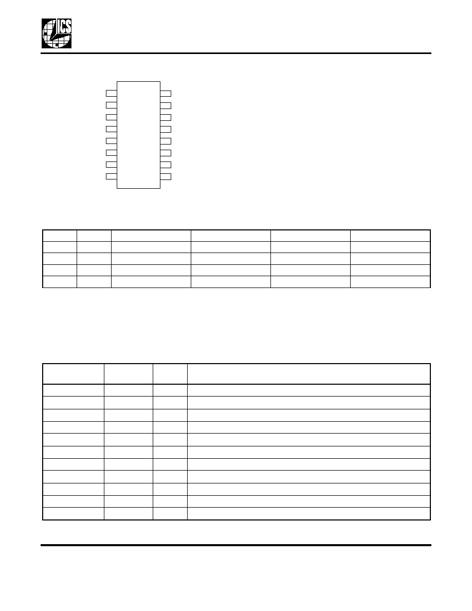
Pin Assignment
Output Clock Mode Select Table
Note 1. Outputs are in high impedence state
Note 2: In S1:S0 = 01 Mode, only the x1 output on CLK 8 will be zero delay. The x2 and x5 outputs can power-up
in different states so the skew relationship is not defined.
Pin Descriptions
1 2
1
1 1
2
1 0
C L K IN
F B IN
3
9
C L K 1
4
C L K 2
C L K 8
5
V D D
6
C L K 7
7
G N D
8
C L K 3
V D D
G N D
C L K 6
C L K 4
C L K 5
S 0
S 1
1 6
1 5
1 4
1 3
1 6 p in n a rro w (1 5 0 m il) S O IC
S1
S0
CLK1:6
CLK7
CLK8
Input Range
0
0
Tri-state (note 1)
Tri-state (note 1)
Tri-state (note 1)
-
0
1
x2 (note 2)
x5 (note 2)
x1
5 to 30 MHz
1
0
x2
x2
x2
15 to 80 MHz
1
1
x4
x4
x4
7.5 to 40 MHz
Pin
Number
Pin
Name
Pin Type
Pin Description
1
CLKIN
Input
Clock input.
2-3, 6-7, 10-11
CLK1:6
Output
Clock outputs 1:6. See table above.
4
VDD
Power
Power supply. Connect both pins to the same voltage (either 3.3V or 5V).
5
GND
Power
Connect to ground.
8
S0
Input
Select input 0. See table above.
9
S1
Input
Select input 1. See table above.
12
GND
Power
Connect to ground.
13
VDD
Power
Power supply. Connect both pins to the same voltage (either 3.3V or 5V).
14
CLK7
Output
Clock output 7. See table above.
15
CLK8
Output
Clock output 8. See table above. Normally use this clock as feedback.
16
FBIN
Input
Feedback input. Connect to CLK8 under normal operations.

Z
ERO
D
ELAY
, L
OW
S
KEW
B
UFFER
AND
MDS 671-01 C
3
Revision 111502
I n t e g r a t e d C i r c u i t S y s t e m s
l
5 2 5 R a c e St r e e t , S a n J o s e , C A 9 5 1 2 6
l
t e l ( 4 0 8 ) 2 9 5 - 9 8 0 0
l
w w w. i c s t . c o m
ICS671-01
External Components
The ICS671-01 requires a minimum number of external components for proper operation. Decoupling
capacitors of 0.01mF should be connected between VDD and GND on pins 4 and 5, and VDD and GND on
pins 13 and 12, as close to the device as possible. A series termination resistor of 33W may be used to
each clock output pin to reduce reflections.
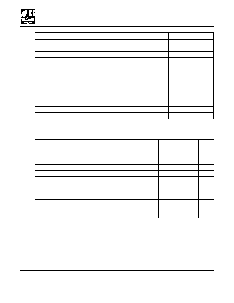
Absolute Maximum Ratings
Stresses above the ratings listed below can cause permanent damage to the ICS671-01. These ratings,
which are standard values for ICS commercially rated parts, are stress ratings only. Functional operation of
the device at these or any other conditions above those indicated in the operational sections of the
specifications is not implied. Exposure to absolute maximum rating conditions for extended periods can
affect product reliability. Electrical parameters are guaranteed only over the recommended operating
temperature range.
Recommended Operation Conditions
DC Electrical Characteristics
VDD=3.3V ±10%,
Ambient temperature 0 to +70
∞
C, unless stated otherwise
Item
Rating
Supply Voltage, VDD
7V
All Inputs and Outputs
-0.5V to VDD+0.5V
CLKIN and FBIN inputs
-0.5V to 5.5V
Electrostatic Discharge
2000 V
Ambient Operating Temperature
0 to +70
∞
C
Storage Temperature
-65 to +150
∞
C
Junction Temperature
150
∞
C
Soldering Temperature
260
∞
C
Parameter
Min.
Typ.
Max.
Units
Ambient Operating Temperature
0
+70
∞
C
Power Supply Voltage (measured in respect to GND)
+3.13
+5.50
V
Parameter
Symbol
Conditions
Min.
Typ.
Max.
Units
Operating Voltage
VDD
3.13
5.5
V
Input High Voltage
V
IH
CLKIN
VDD/2+1
VDD/2
V
Input Low Voltage
V
IL
CLKIN
VDD/2 VDD/2-1
V
Input High Voltage
V
IH
2
V
Input Low Voltage
V
IL
0.8
V
Z
ERO
D
ELAY
, L
OW
S
KEW
B
UFFER
AND
MDS 671-01 C
4
Revision 111502
I n t e g r a t e d C i r c u i t S y s t e m s
l
5 2 5 R a c e St r e e t , S a n J o s e , C A 9 5 1 2 6
l
t e l ( 4 0 8 ) 2 9 5 - 9 8 0 0
l
w w w. i c s t . c o m
ICS671-01
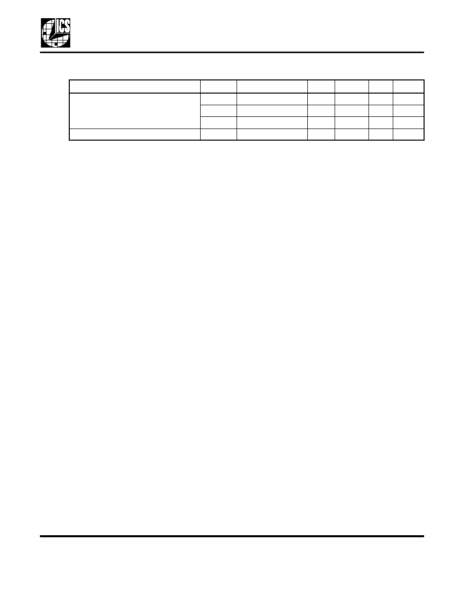
AC Electrical Characteristics
VDD = 3.3V ±10%, Ambient Temperature 0to +70
∞
C, C
LOAD
at CLK = 15 pF, unless stated otherwise
Note 1: With CLKIN = 20 MHz, FBIN to CLK8, all outputs at 40 MHz
Note 2:With CLKIN = 80 MHz, FBIN to CLK8, all outputs at 160 MHz
Note 3: These specs do not apply to mode 01
Input Low Current
I
IL
VIN = 0V
50
µ
A
Input High Current
I
IH
VIN = VDD
100
µ
A
Output High Voltage
V
OH
I
OH
= -25 mA
2.4
V
Ouput Low Voltage
V
OL
I
OL
= 25mA
0.4
V
Output High Voltage,
CMOS level
V
OH
I
OH
= -8 mA
VDD-0.4
V
Operating Supply Current
IDD
No Load, S1 = 1, S0 = 0,
Note 1
25
mA
No Load, S1 = 1, S0 =0
Note 2
Power Down Supply
Current
IDDPD
CLKIN = 0, S0 = 0, S1 = 0
500
µ
A
Short Circuit Current
I
OS
Each output
±50
mA
Input Capacitance
C
IN
S0, S1, FBIN
7
pF
Parameter
Symbol
Conditions
Min.
Typ.
Max.
Units
Parameter
Symbol
Conditions
Min.
Typ.
Max.
Units
Input Clock Frequency
f
IN
See table on page 2
5
80
MHz
Output Clock Frequency
See table on page 2
5
160
MHz
Output Rise Time
t
OR
0.8 to 2.0V, CL=30pF
1.5
ns
Output Fall Time
t
OF
2.0 to 0.8V, CL=30pF
1.5
ns
Output Clock Duty Cycle
t
DC
measured at VDD/2
40
50
60
%
Device to Device Skew
rising edges at VDD/2, Note 3
700
ps
Output to Output Skew
rising edges at VDD/2, Note 3
250
ps
Input to Output Skew
rising edges at VDD/2, FBIN to
CLK8
±350
ps
Maximum Absolute JItter
15pF
300
ps
Cycle to Cycle Jitter
30pF loads
500
ps
PLL Lock Time
Note 3
1.0
ms
Z
ERO
D
ELAY
, L
OW
S
KEW
B
UFFER
AND
MDS 671-01 C
5
Revision 111502
I n t e g r a t e d C i r c u i t S y s t e m s
l
5 2 5 R a c e St r e e t , S a n J o s e , C A 9 5 1 2 6
l
t e l ( 4 0 8 ) 2 9 5 - 9 8 0 0
l
w w w. i c s t . c o m
ICS671-01
Thermal Characteristics (16 pin SOIC)
Parameter
Symbol
Conditions
Min.
Typ.
Max.
Units
Thermal Resistance Junction to
Ambient
JA
Still air
120
∞
C/W
JA
1 m/s air flow
115
∞
C/W
JA
3 m/s air flow
105
∞
C/W
Thermal Resistance Junction to Case
JC
58
∞
C/W

Z
ERO
D
ELAY
, L
OW
S
KEW
B
UFFER
AND
MDS 671-01 C
6
Revision 111502
I n t e g r a t e d C i r c u i t S y s t e m s
l
5 2 5 R a c e St r e e t , S a n J o s e , C A 9 5 1 2 6
l
t e l ( 4 0 8 ) 2 9 5 - 9 8 0 0
l
w w w. i c s t . c o m
ICS671-01
Package Outline and Package Dimensions
(16 pin SOIC, 150 Mil. Narrow Body)
Package dimensions are kept current with JEDEC Publication No. 95
Ordering Information
While the information presented herein has been checked for both accuracy and reliability, Integrated Circuit Systems (ICS) assumes no
responsibility for either its use or for the infringement of any patents or other rights of third parties, which would result from its use. No other
circuits, patents, or licenses are implied. This product is intended for use in normal commercial applications. Any other applications such as
those requiring extended temperature range, high reliability, or other extraordinary environmental requirements are not recommended without
additional processing by ICS. ICS reserves the right to change any circuitry or specifications without notice. ICS does not authorize or warrant
any ICS product for use in life support devices or critical medical instruments.
Part / Order Number
Marking
Shipping
packaging
Package
Temperature
ICS671M-01
ICS671M-01
Tubes
16 pin SOIC
0 to +70
∞
C
ICS671M-01T
ICS671M-01
Tape and Reel
16 pin SOIC
0 to +70
∞
C
INDEX
AREA
1 2
16
D
E
SEATING
PLANE
A1
A
e
- C -
B
.10 (.004)
C
C
L
H
h x 45
Millimeters
Inches
Symbol
Min
Max
Min
Max
A
1.35
1.75
.0532
.0688
A1
0.10
0.25
.0040
.0098
B
0.33
0.51
.013
.020
C
0.19
0.25
.0075
.0098
D
9.80
10.00
.3859
.3937
E
3.80
4.00
.1497
.1574
e
1.27 BASIC
0.050 BASIC
H
5.80
6.20
.2284
.2440
h
0.25
0.50
.010
.020
L
0.40
1.27
.016
.050
0
∞
8
∞
0
∞
8
∞