 | –≠–ª–µ–∫—Ç—Ä–æ–Ω–Ω—ã–π –∫–æ–º–ø–æ–Ω–µ–Ω—Ç: 672-02 | –°–∫–∞—á–∞—Ç—å:  PDF PDF  ZIP ZIP |
ICS672-01/02
QuadraClockTM Quadrature Delay Buffer
MDS 672-01/02 D
1
Revision 091701
Integrated Circuit Systems, Inc.∑ 525 Race Street ∑ San Jose ∑CA∑95126∑ (408) 295-9800 tel ∑ www.icst.com
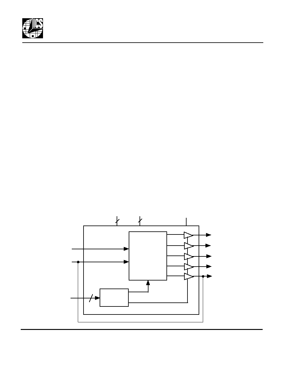
Block Diagram
Description
Features
The ICS672-01 and ICS672-02 are zero delay buffers
that generate four output clocks whose phases are
spaced at 90∞ intervals. Based on ICS' proprietary low
jitter Phase Locked Loop (PLL) techniques, each
device provides five low skew outputs, with clock rates
up to 84 MHz for the ICS672-01 and up to 135 MHz for
the ICS672-02. By providing outputs delayed one
quarter clock cycle, the device is useful for systems
requiring early or late clocks.
The ICS672-01/02 include multiplier selections of
x0.5, x1, x2, x3, x4, x5, or x6. They also offer a mode
to power down all internal circuitry and tri state the
outputs. In normal operation, output clock FBCLK is
tied to the FBIN pin.
ICS manufactures the largest variety of clock
generators and buffers, and is the largest clock
supplier in the world.
∑ Packaged in 16 pin narrow SOIC
∑ Input clock range from 5 MHz to 150 MHz (depends on
multiplier)
∑ Clock outputs from up to 84 MHz (ICS672-01)
and up to 135 MHz (ICS672-02)
∑ Zero input-output delay
∑ Integrated x0.5, x1, x2, x3, x4, x5, or x6 selections
∑ Four accurate (<250 ps) outputs with 0∞, 90∞,
180∞, and 270∞ phase shift from ICLK, and one
FBCLK (0∞)
∑ Separate supply for output clocks from 2.5V to 5V
∑ Full CMOS outputs (TTL compatible)
∑ Tri state mode for board-level testing
∑ Includes Power Down for power savings
∑ Advanced, low power, sub-micron CMOS process
∑ 3.3 V to 5 V operating voltage
∑ Industrial temperature version available
PLL
Multiplier
and
Quadrature
Generation
FBIN
S2:S0
3
CLK0
CLK90
CLK180
CLK270
CLKFB
Control
Logic
IN
GND
VDDIO
VDD
2
3
Power Down + Tri-State
External Feedback
ICS672-01/02
QuadraClockTM Quadrature Delay Buffer
MDS 672-01/02 D
2
Revision 091701
Integrated Circuit Systems, Inc.∑ 525 Race Street ∑ San Jose ∑CA∑95126∑ (408) 295-9800 tel ∑ www.icst.com
Pin Descriptions
Key: I = Input; O = output; P = power supply connection.
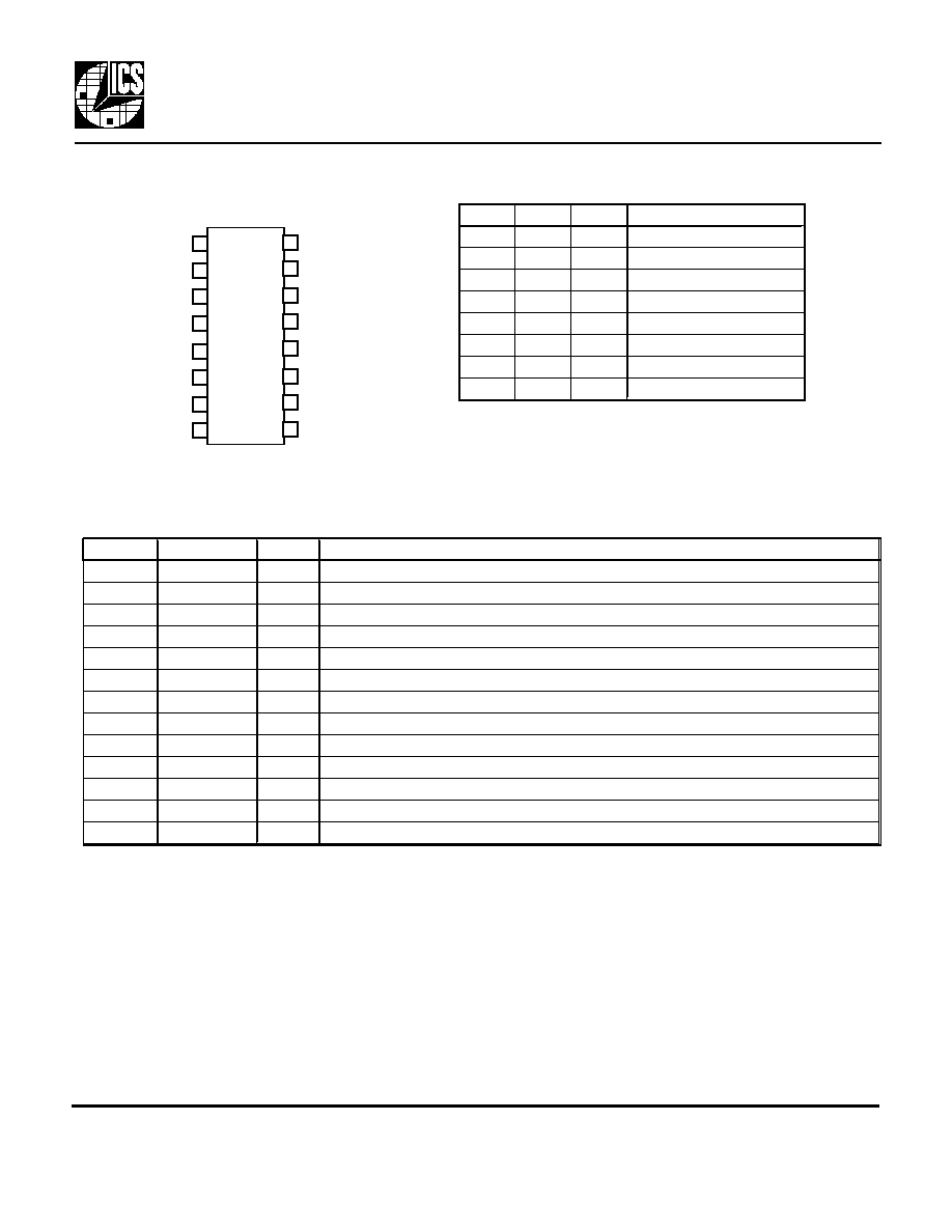
Pin Assignment
External Components
The ICS672-01/01 requires a minimum number of external components for proper operation. Decoupling capacitors
of 0.01µF should be connected between VDD and GND on pins 11 and 12, VDD and GND on pins 13 and 12, and
VDDIO and GND on pins 5 and 6, as close to the device as possible. A series termination resistor of 33
may be
used close to each clock output pin to reduce reflections.
16
15
14
13
16 pin narrow (150 mil) SOIC
12
11
10
9
1
2
3
4
5
6
7
8
CLK90
VDDIO
FBIN
ICLK
CLK270
S0
GND
GND
VDD
GND
S2
S1
VDD
FBCLK
CLK0
CLK180
Number
Name
Type
Description
1
ICLK
I
Clock Input.
2
CLK90
O
Clock Output (90∞ delayed from CLK0).
3
CLK180
O
Clock Output (180∞ delayed from CLK0).
4
CLK270
O
Clock Output (270∞ delayed from CLK0).
5
VDDIO
P
Supply voltage for input and output clocks. Must not exceed VDD.
6, 7, 12
GND
P
Connect to ground.
8
S0
I
Select input 0. See table above.
9
S1
I
Select input 1. See table above.
10
S2
I
Select input 2. See table above.
11, 13
VDD
P
Connect to +3.3 V or +5.0 V.
14
CLK0
O
Clock Output phase aligned to ICLK.
15
FBCLK
O
Feedback Clock Output (0∞ phase shift from CLK0).
16
FBIN
I
Feedback Clock Input. In normal operation, connect to FBCLK
S2
S1
S0
Output Clocks
0
0
0
Power Down + Tri State
0
0
1
x1
0
1
0
x2
0
1
1
x3
1
0
0
x4
1
0
1
x5
1
1
0
x6
1
1
1
x0.5
Output Clock Mode Select Table
ICS672-01/02
QuadraClockTM Quadrature Delay Buffer
MDS 672-01/02 D
3
Revision 091701
Integrated Circuit Systems, Inc.∑ 525 Race Street ∑ San Jose ∑CA∑95126∑ (408) 295-9800 tel ∑ www.icst.com
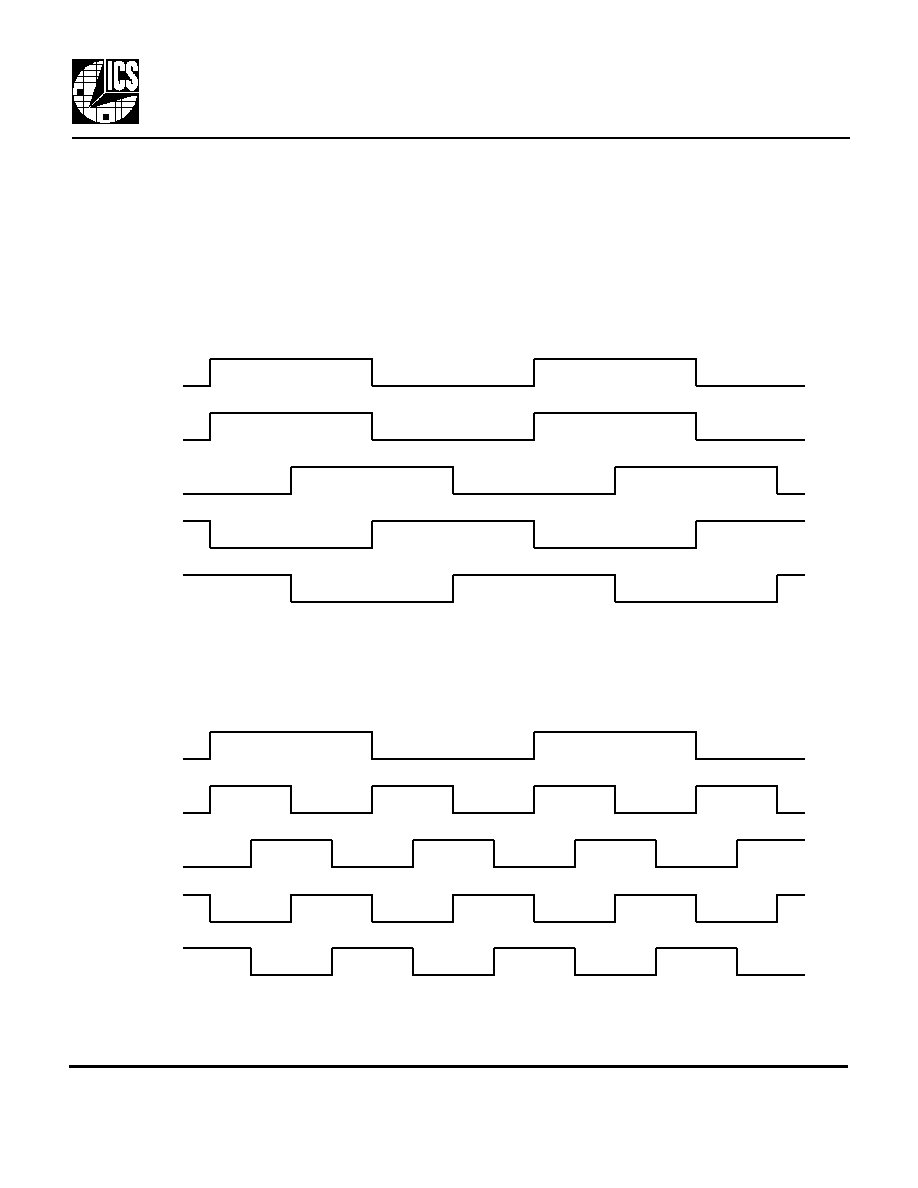
Operation and Applications
The ICS672-01/02 each provide a total of five output clocks with multiple phase shifts relative to the input clock
(ICLK). Phase shifts of 0∞ (CLK0), 90∞ (CLK90), 180∞ (CLK180), and 270∞ (CLK270) are provided, plus one feedback
clock (FBCLK). All output clocks will be a multiple of the input clock, as determined by the table on page 2. Refer to
the illustrations in Figure 1 and Figure 2.
FBCLK is connected to the feedback input (FBIN) to provide a zero delay through the ICS672-01/02. FBCLK has a 0∞
phase shift from ICLK.
Figure 1. Phase alignment of input and output clocks. (x1 multiplier)
CLK90
CLK180
CLK0,
FBCLK
CLK270
ICLK
Figure 2. Phase alignment of input and output clocks. (x2 multiplier)
CLK90
CLK180
CLK0,
FBCLK
CLK270
ICLK
ICS672-01/02
QuadraClockTM Quadrature Delay Buffer
MDS 672-01/02 D
4
Revision 091701
Integrated Circuit Systems, Inc.∑ 525 Race Street ∑ San Jose ∑CA∑95126∑ (408) 295-9800 tel ∑ www.icst.com
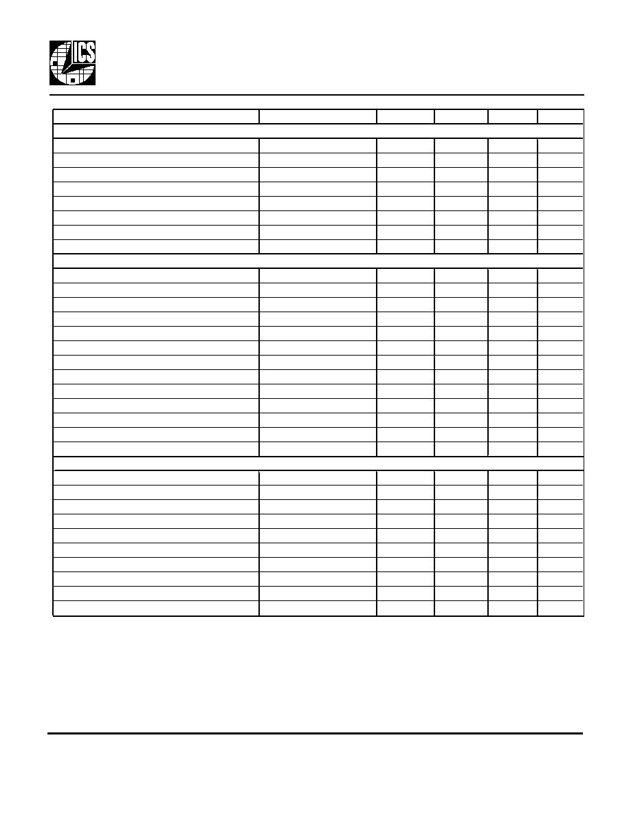
Parameter
Conditions
Minimum
Typical
Maximum
Units
ABSOLUTE MAXIMUM RATINGS (note 1)
ABSOLUTE MAXIMUM RATINGS (note 1)
Supply voltage, VDD & VDDIO
Referenced to GND
-0.5
7
V
Inputs and Clock Outputs
Referenced to GND
-0.5
VDD+0.5
V
Electrostatic Discharge
MIL-STD-883
2000
V
Ambient Operating Temperature
0
70
∞C
Ambient Operating Temperature, Industrial
Available on -02 only
-40
85
∞C
Soldering Temperature
Max of 10 seconds
260
∞C
Junction temperature
150
∞C
Storage temperature
-65
150
∞C
DC CHARACTERISTICS (VDD =VDDIO = 3.3 V unless specified otherwise)
DC CHARACTERISTICS (VDD =VDDIO = 3.3 V unless specified otherwise)
DC CHARACTERISTICS (VDD =VDDIO = 3.3 V unless specified otherwise)
DC CHARACTERISTICS (VDD =VDDIO = 3.3 V unless specified otherwise)
Operating Voltage, VDD
3.13
5.50
V
Operating Voltage, VDDIO
2.375
VDD
V
Input High Voltage, VIH, ICLK only
VDD/2+1
V
Input Low Voltage, VIL, ICLK only
VDD/2-1
V
Input High Voltage, VIH
2
V
Input Low Voltage, VIL
0.8
V
Output High Voltage, VOH
IOH=-12 mA
2.4
V
Output Low Voltage, VOL
IOL=12 mA
0.4
V
Output High Voltage, VOH, CMOS level
IOH=-8mA
VDDIO-0.4
V
Operating Supply Current, IDD (Note 2)
No Load, S1=1, S0=0, S2=0
11
mA
Operating Supply Current, IDD (Note 3)
No Load, S1=1, S0=0, S2=0
22
mA
Short Circuit Current
Each output
±50
mA
Input Capacitance
7
pF
AC CHARACTERISTICS (VDD = VDDIO = 3.3 V unless specified otherwise)
AC CHARACTERISTICS (VDD = VDDIO = 3.3 V unless specified otherwise)
AC CHARACTERISTICS (VDD = VDDIO = 3.3 V unless specified otherwise)
AC CHARACTERISTICS (VDD = VDDIO = 3.3 V unless specified otherwise)
Input Clock Frequency (Note 4)
5
150
MHz
Output Clock Frequency
ICS672-01
15
84
MHz
Output Clock Frequency
ICS672-02
15
135
MHz
Output Clock Rise Time, CL = 15 pF
0.8 to 2.0V
1.5
ns
Output Clock Fall Time, CL = 15 pF
2.0 to 0.8V
1.5
ns
Output Clock Duty Cycle, VDDIO=3.3V
At VDDIO/2
45
50
55
%
Phased Outputs Accuracy (Note 5)
rising edges at VDDIO/2
-250
250
ps
Input to Output Skew, ICLK to CLK0 (Note 6)
-300
300
ps
Maximum Absolute Jitter
75
ps
Cycle to Cycle Jitter, 15 pF loads
150
ps
Electrical Specifications
Notes: 1. Stresses beyond those listed under Absolute Maximum Ratings could cause permanent damage to the
device. Prolonged exposure to levels above the operating limits but below the Absolute Maximums may
affect device reliability.
2. With ICLK = 20 MHz, FBCLK to FBIN, all outputs at 40 MHz.
3. With ICLK = 66.5 MHz, FBCLK to FBIN, all outputs at 133 MHz.
4. Value depends on multiplier. Must also meet output clock frequency.
5. With CLK0:CLK270 equally loaded, and output frequency > 60 MHz.
6. Rising edge of ICLK compared with rising edge of CLK0, with FBCLK connected to FBIN, 15 pF load on
CLK0, and CLK0 > 60 MHz.
ICS672-01/02
QuadraClockTM Quadrature Delay Buffer
MDS 672-01/02 D
5
Revision 091701
Integrated Circuit Systems, Inc.∑ 525 Race Street ∑ San Jose ∑CA∑95126∑ (408) 295-9800 tel ∑ www.icst.com
While the information presented herein has been checked for both accuracy and reliability, Integrated Circuit Systems,
Incorporated (ICS) assumes no responsibility for either its use or for the infringement of any patents or other rights of third
parties, which would result from its use. No other circuits, patents, or licenses are implied. This product is intended for use in
normal commercial applications. Any other applications such as those requiring extended temperature range, high reliability, or
other extraordinary environmental requirements are not recommended without additional processing by ICS. ICS reserves the
right to change any circuitry or specifications without notice. ICS does not authorize or warrant any ICS product for use in life
support devices or critical medical instruments.
Ordering Information
Part/Order Number
Marking
Shipping packaging
Package
Temperature
ICS672M-01
ICS672M-01
tubes
16 pin SOIC
0 to 70 ∞C
ICS672M-01T
ICS672M-01
tape and reel
16 pin SOIC
0 to 70 ∞C
ICS672M-02
ICS672M-02
tubes
16 pin SOIC
0 to 70 ∞C
ICS672M-02T
ICS672M-02
tape and reel
16 pin SOIC
0 to 70 ∞C
ICS672M-02I
ICS672M-02I
tubes
16 pin SOIC
-40 to 85 ∞C
ICS672M-02IT
ICS672M-02I
tape and reel
16 pin SOIC
-40 to 85 ∞C
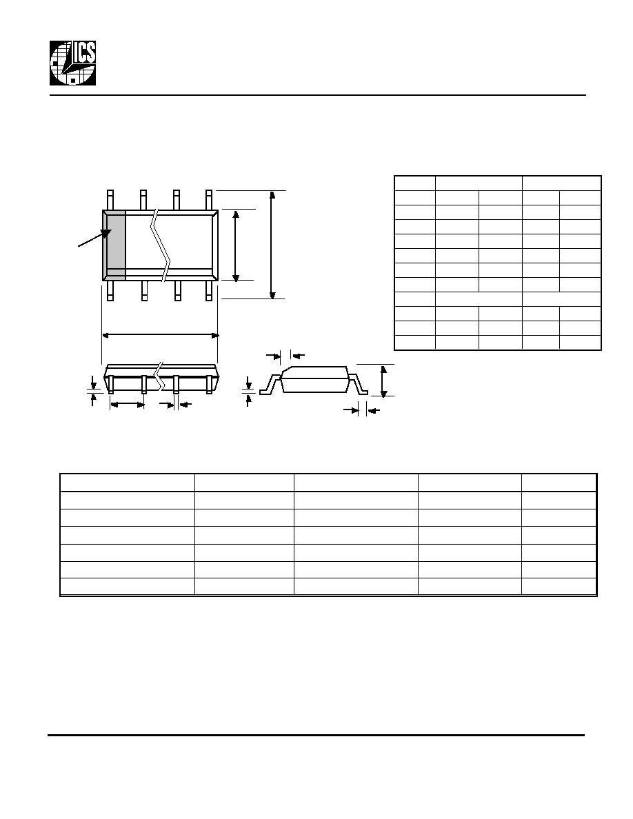
16 pin SOIC narrow
Inches
Inches
Millimeters
Millimeters
Symbol
Min
Max
Min
Max
A
0.0532
0.0688
1.35
1.75
A1
0.0040
0.0098
0.10
0.24
B
0.0130
0.0200
0.33
0.51
C
0.0075
0.0098
0.19
0.24
D
0.3859
0.3937
9.80
10.00
E
0.1497
0.1574
3.80
4.00
e .050 BSC
.050 BSC
1.27 BSC
1.27 BSC
H
0.2284
0.2440
5.80
6.20
h
0.0099
0.0195
0.25
0.50
L
0.0160
0.0500
0.41
1.27
B
D
E
H
e
A1
C
A
h x 45∞
L
INDEX
AREA
1
2
Package Outline and Package Dimensions
(For current dimensional specifications, see JEDEC Publication No. 95.)