
ICS673-01
MDS 673-01 H
1
Revision 033103
I n t e g r a t e d C i r cu i t S y st e m s
q
5 2 5 Ra ce S t r e e t , S a n J o s e , C A 9 5 1 2 6
q
t e l ( 4 0 8 ) 2 9 5 - 9 8 0 0
q
w w w. i c s t . c o m
PLL B
UILDING
B
LOCK
Description
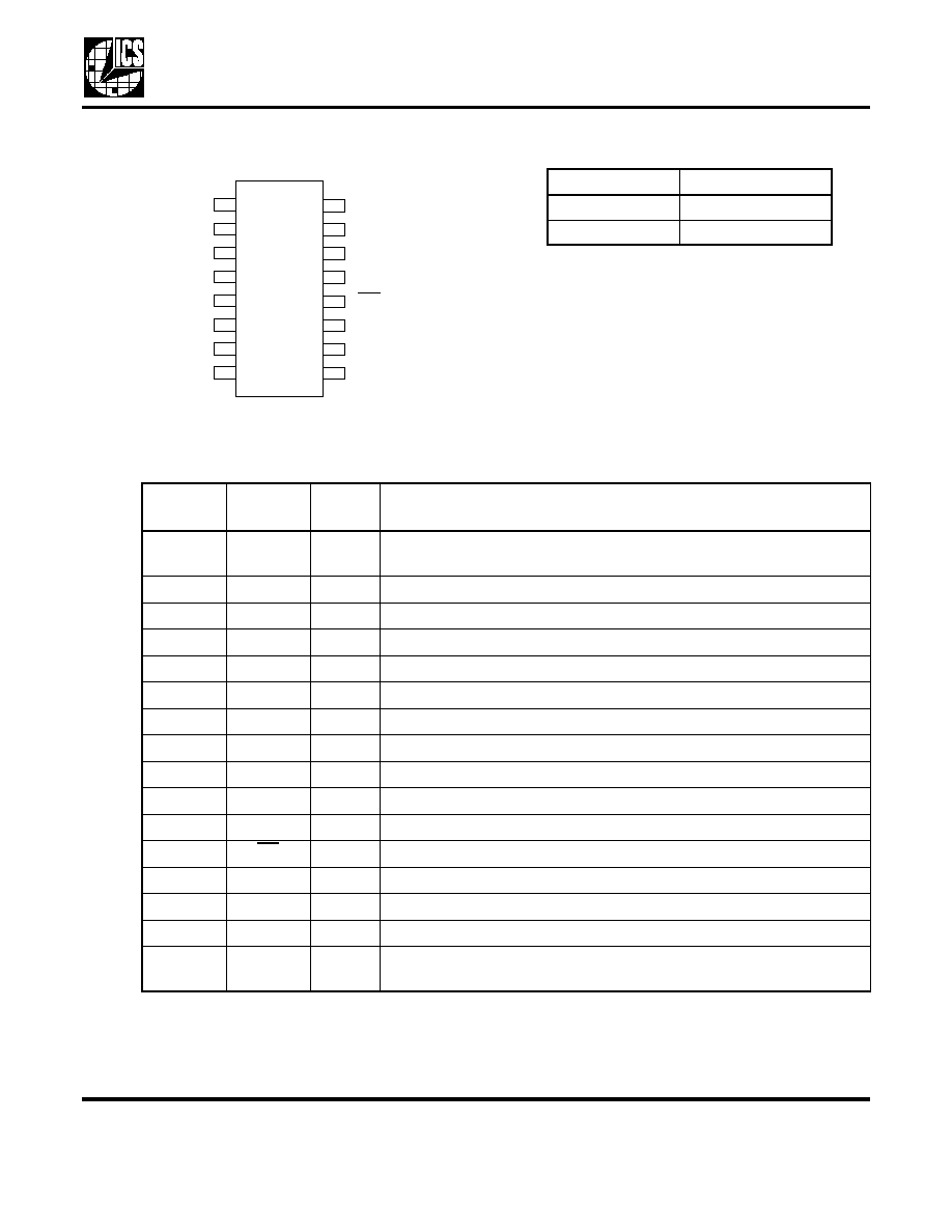
The ICS673-01 is a low cost, high performance Phase
Locked Loop (PLL) designed for clock synthesis and
synchronization. Included on the chip are the phase
detector, charge pump, Voltage Controlled Oscillator
(VCO), and two output buffers. One output buffer is a
divide by two of the other. Through the use of external
reference and VCO dividerslthe ICS674-01), the user
can customize the clock to lock to a wide variety of
input frequencies.
The ICS673-01 also has an output enable function that
puts both outputs into a high-impedance state. The
chip also has a power down feature which turns off the
entire device.
For applications that require low jitter or jitter
attenuation, see the MK2069. For a smaller package,
see the ICS663.
Features
�
Packaged in 16 pin SOIC
�
Access to VCO input and feedback paths of PLL
�
VCO operating range up to 120 MHz (5V)
�
Able to lock MHz range outputs to kHz range inputs
through the use of external dividers
�
Output Enable tri-states outputs
�
Low skew output clocks
�
Power Down turns off chip
�
VCO predivide to feedback divider of 1 or 4
�
25 mA output drive capability at TTL levels
�
Advanced, low power, sub-micron CMOS process
�
+3.3 V +5 V +10% operating voltage
�
Industrial temperature range available
�
Forms a complete PLL, using the ICS674-01
�
For better jitter performance, please use the
ICS1575
Block Diagram
REFIN
Phase/
Frequency
Detector
VCO
4
2
SEL
VCOIN
CHCP
UP
FBIN
DOWN
I
cp
I
cp
CLK2
VDD
MUX
1
0
External Feedback Divider
(such as the ICS674-01)
Clock Input
CAP
PD
(entire chip)
VDD
2
3
GND
CLK1
OE
(both
outputs)
PLL B
UILDING
B
LOCK
MDS 673-01 H
2
Revision 033103
I n t e g r a t e d C i r c u i t S y s t e ms
q
5 2 5 R a c e S t r e e t , S a n J o s e , CA 9 5 1 2 6
q
t e l ( 4 0 8 ) 2 9 5 - 9 8 0 0
q
w w w. ic s t . c o m
ICS673-01
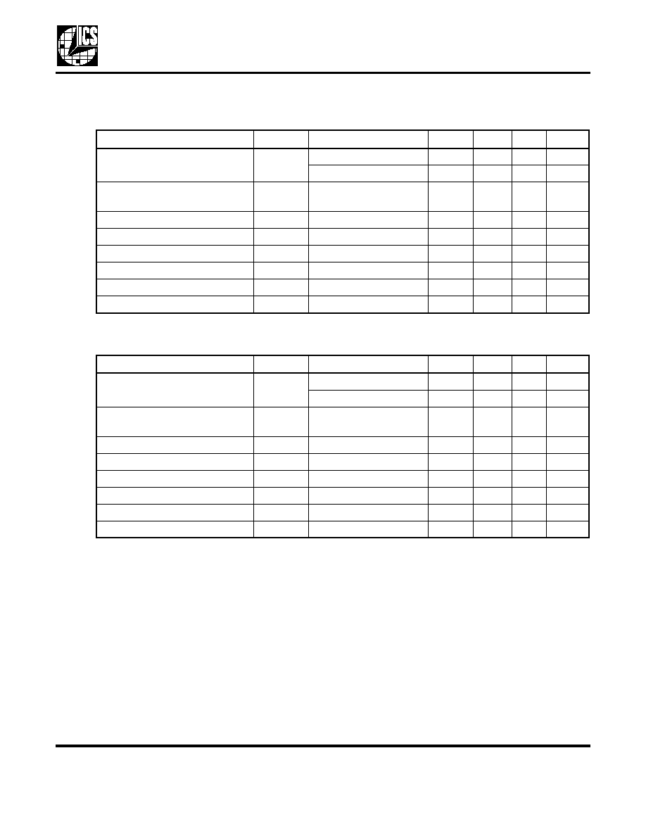
Pin Assignment
VCO Predivide Select Table
0 = connect pin directly to ground
1 = connect pin directly to VDD
Pin Descriptions
1 2
1
1 1
2
1 0
F B IN
R E F IN
3
9
V D D
4
V D D
N C
5
G N D
6
C L K 1
7
G N D
8
G N D
C L K 2
P D
S E L
C H G P
O E
V C O IN
C A P
1 6
1 5
1 4
1 3
1 6 p in n a rro w (1 5 0 m il) S O IC
SEL
VCO Predivide
0
4
1
1
Pin
Number
Pin
Name
Pin
Type
Pin Description
1
FBIN
Input
Feedback clock input. Connect the feedback clock to this pin. Falling
edge triggered.
2
VDD
Power
Connect to +3.3 V or +5 V and to VDD on pin 3.
3
VDD
Power
Connect to VDD on pin 2.
4
GND
Power
Connect to ground.
5
GND
Power
Connect to ground.
6
GND
Power
Connect to ground.
7
CHGP
Output
Charge pump output. Connect to VCOIN under normal operation.
8
VCOIN
Input
Input to internal VCO.
9
CAP
Input
Loop filter return.
10
OE
Input
Output enable. Active when high. Tri-states both outputs when low.
11
SEL
Input
Select pin for VCO predivide to feedback divider per table above.
12
PD
Input
Power down. Turns off entire chip when pin is low. Outputs stop low.
13
CLK2
Output
Clock output 2. Low skew divide by two version of CLK1.
14
CLK1
Output
Clock output 1.
15
NC
-
No connect. Nothing is connected internally to this pin.
16
REFIN
Input
Reference input. Connect reference clock to this pin. Falling edge is
triggered.

PLL B
UILDING
B
LOCK
MDS 673-01 H
3
Revision 033103
I n t e g r a t e d C i r c u i t S y s t e ms
q
5 2 5 R a c e S t r e e t , S a n J o s e , CA 9 5 1 2 6
q
t e l ( 4 0 8 ) 2 9 5 - 9 8 0 0
q
w w w. ic s t . c o m
ICS673-01
Absolute Maximum Ratings
Stresses above the ratings listed below can cause permanent damage to the ICS673-01. These ratings,
which are standard values for ICS commercially rated parts, are stress ratings only. Functional operation of
the device at these or any other conditions above those indicated in the operational sections of the
specifications is not implied. Exposure to absolute maximum rating conditions for extended periods can
affect product reliability. Electrical parameters are guaranteed only over the recommended operating
temperature range.
Recommended Operation Conditions
DC Electrical Characteristics
VDD=3.3V �5% or 5.0V �10%,
Ambient temperature -40 to +85
�
C, unless stated otherwise
Item
Rating
Supply Voltage, VDD
7V
All Inputs and Outputs
-0.5V to VDD+0.5V
Ambient Operating Temperature
0 to +70
�
C
Industrial Temperature
-40 to +85
�
C
Storage Temperature
-65 to +150
�
C
Soldering Temperature
260
�
C
Parameter
Min.
Typ.
Max.
Units
Ambient Operating Temperature
0
+70
�
C
Power Supply Voltage (measured in respect to GND)
+3.13
+5.25
V
Parameter
Symbol
Conditions
Min.
Typ.
Max.
Units
Operating Voltage
VDD
3.13
5.50
V
Logic Input High Voltage
V
IH
REFIN, FBIN,
SEL
2
V
Logic Input Low Voltage
V
IL
REFIN, FBIN,
SEL
0.8
V
LF Input Voltage Range
V
I
0
VDD
V
Output High Voltage
V
OH
I
OH
= -25 mA
2.4
V
Output Low Voltage
V
OL
I
OL
= 25mA
0.4
V
Output High Voltage, CMOS
level
V
OH
I
OH
= -8 mA
VDD-0.4
Operating Supply Current
IDD
VDD = 5.0 V,
No load, 40 MHz
15
mA
Short Circuit Current
I
OS
CLK
�100
mA
Input Capacitance
C
I
SEL
5
pF
PLL B
UILDING
B
LOCK
MDS 673-01 H
4
Revision 033103
I n t e g r a t e d C i r c u i t S y s t e ms
q
5 2 5 R a c e S t r e e t , S a n J o s e , CA 9 5 1 2 6
q
t e l ( 4 0 8 ) 2 9 5 - 9 8 0 0
q
w w w. ic s t . c o m
ICS673-01
AC Electrical Characteristics
VDD = 3.3V �5%,
Ambient Temperature -40 to +85
�
C, C
LOAD
at CLK = 15 pF, unless stated otherwise
VDD = 5.0V �10%,
Ambient Temperature -40 to +85
�
C, C
LOAD
at CLK = 15 pF,
unless stated otherwise
Note 1: Minimum input frequency is limited by loop filter design. 1 kHz is a practical minimum limit.
External Components
The ICS673-01 requires a minimum number of external
components for proper operation. A decoupling
capacitor of 0.01
�
F should be connected between
VDD and GND as close to the ICS673-01 as possible.
A series termination resistor of 33
may be used at
the clock output.
Special considerations must be made in choosing loop
components C
1
and C
2
:
1) The loop capacitors should be a low-leakage type to
avoid leakage-induced phase noise. For this reason,
DO NOT use any type of polarized or electrolytic
capacitors.
2) Microphonics (mechanical board vibration) can also
induce output phase noise when the loop bandwidth is
less than 1kHz. For this reason, ceramic capacitors
should have C0G or NP0 dielectric. Avoid high-K
dielectrics like Z5U and X7R. These and some other
Parameter
Symbol
Conditions
Min.
Typ.
Max.
Units
Output Clock Frequency
(from pin CLK)
f
CLK
SEL = 1
1
100
MHz
SEL = 0
0.25
25
MHz
Input Clock Frequency
(into pins REFIN or FBIN)
f
REF
Note 1
8
MHz
Output Rise Time
t
OR
0.8 to 2.0V
1.2
2
ns
Output Fall Time
t
OF
2.0 to 0.8V
0.75
1.5
ns
Output Clock Duty Cycle
t
DC
At VDD/2
40
50
60
%
Jitter, Absolute peak-to-peak
t
J
250
ps
VCO Gain
K
O
TBD
MHz/V
Charge Pump Current
I
cp
2.5
�
A
Parameter
Symbol
Conditions
Min.
Typ.
Max.
Units
Output Clock Frequency
(from pin CLK)
f
CLK
SEL = 1
1
120
MHz
SEL = 0
0.25
30
MHz
Input Clock Frequency
(into pins REFIN or FBIN)
f
REF
Note 1
8
MHz
Output Rise Time
t
OR
0.8 to 2.0V
0.5
1
ns
Output Fall Time
t
OF
2.0 to 0.8V
0.5
1
ns
Output Clock Duty Cycle
t
DC
At VDD/2
45
50
55
%
Jitter, Absolute peak-to-peak
t
J
150
ps
VCO Gain
K
O
200
MHz/V
Charge Pump Current
I
cp
2.5
�
A
PLL B
UILDING
B
LOCK
MDS 673-01 H
5
Revision 033103
I n t e g r a t e d C i r c u i t S y s t e ms
q
5 2 5 R a c e S t r e e t , S a n J o s e , CA 9 5 1 2 6
q
t e l ( 4 0 8 ) 2 9 5 - 9 8 0 0
q
w w w. ic s t . c o m
ICS673-01
ceramics have piezoelectric properties that convert
mechanical vibration into voltage noise that interferes
with VCO operation.
For larger loop capacitor values such as 0.1
�
F or 1
�
F,
PPS film types made by Panasonic, or metal poly types
made by Murata or Cornell Dubilier are recommended.
For questions or changes regarding loop filter
characteristics, please contact your sales area FAE, or
e-mail telecom@icst.com.
Avoiding PLL Lockup
In some applications, the ICS673-01 can "lock up" at
the maximum VCO frequency. This is usually caused
by power supply glitches or a very slow power supply
ramp. This situation also occurs if the external divider
starts to fail at high input frequencies. The usual failure
mode of a divider circuit is that the output of the divider
begins to miss clock edges. The phase detector
interprets this as a too low output frequency and
increases the VCO frequency. The feedback divider
begins to miss even more clock edges and the VCO
frequency is continually increased until it is running at
its maximum frequency. Whether caused by power
supply issues or by the external divider, the loop can
only recover by powering down the circuit or asserting
PD.
The simplest way to avoid this problem is to use an
external divider that always operates correctly
regardless of the VCO speed. Figures 2 and 3 show
that the VCO is capable of high speeds. By using the
internal divide-by-four and/or the CLK2 output, the
maximum VCO frequency can be divided by 2, 4, or 8
and a slower counter can be used. Using the ICS673
internal dividers in this manner does reduce the
number of frequencies that can be exactly synthesized
by forcing the total VCO divide to change in increments
of 2, 4, or 8.
If this lockup problem occurs, there are several
solutions; three of which are described below.
1. If the system has a reset or power good signal, this
should be applied to the PD pin, forcing the chip to stay
powered down until the power supply voltage has
stabilized
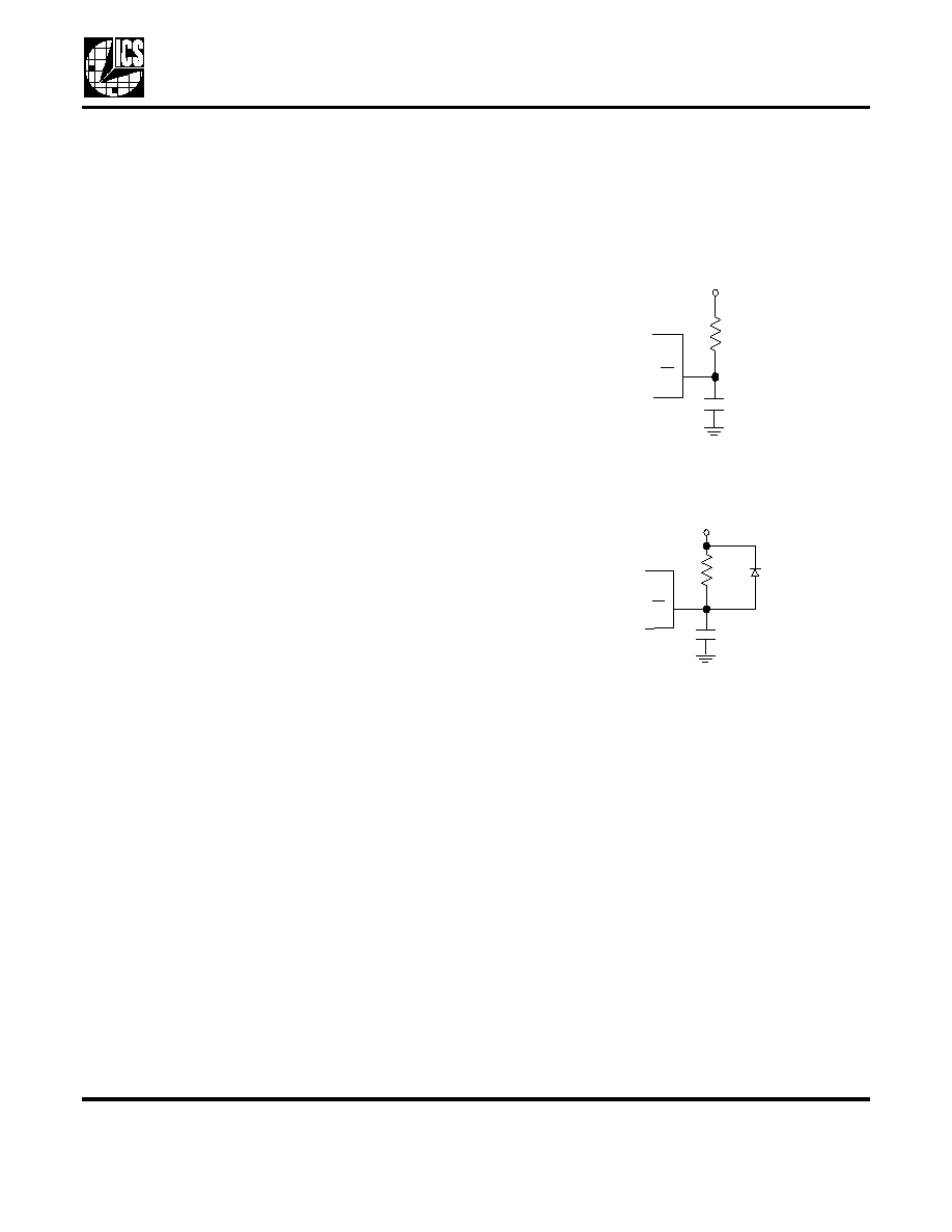
2. If no power good signal is available, a simple
power-on reset circuit can be attached to the PD pin, as
shown in Figure 4. When the power supply ramps up,
this circuit holds PD asserted (device powered down)
until the capacitor charges.
The circuit of Figure 4A is adequate in most cases, but
the discharge rate of capacitor C3 when VDD goes low
is limited by R1. As this discharge rate determines the
minimum reset time, the circuit of Figure 4B may be
used when a faster reset time is desired. The values of
R1 and C3 should be selected to ensure that PD stays
below 1.0 V until the power supply is stable.
3. A comparator circuit may be used to monitor the loop
filter voltage, as shown in Figure 5. This circuit will
dump the charge off the loop filter by asserting PD if the
VCO begins to run too fast and the PLL can recover. A
good choice for the comparator is the National
Semiconductor LMC7211BIM5X. It is low power,
version of the small (SOT-23), low cost, and has high
input impedance.
The trigger voltage of the comparator is set by the
voltage divider formed by R2 and R3. The voltage
A. Ba si c Ci r cui t
R
1
C
3
PD
I CS673 - 01
VDD
B . F a s t e r D i s c h a r g e
R
1
C
3
P D
I C S 6 7 3 - 0 1
V D D
D
1
F i g 1 . P o we r o n Re s e t Ci r c u i t s